Embed Size (px)
Citation preview
November 2009 Doc ID 15179 Rev 2 1/18
18
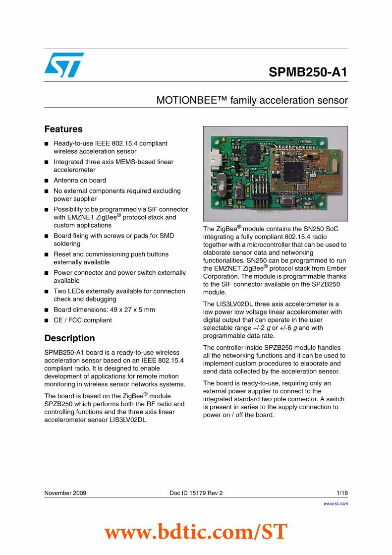
SPMB250-A1
MOTIONBEE™ family acceleration sensor
Features■ Ready-to-use IEEE 802.15.4 compliant
wireless acceleration sensor
■ Integrated three axis MEMS-based linear accelerometer
■ Antenna on board
■ No external components required excluding power supplier
■ Possibility to be programmed via SIF connector with EMZNET ZigBee® protocol stack and custom applications
■ Board fixing with screws or pads for SMD soldering
■ Reset and commissioning push buttons externally available
■ Power connector and power switch externally available
■ Two LEDs externally available for connection check and debugging
■ Board dimensions: 49 x 27 x 5 mm
■ CE / FCC compliant
DescriptionSPMB250-A1 board is a ready-to-use wireless acceleration sensor based on an IEEE 802.15.4 compliant radio. It is designed to enable development of applications for remote motion monitoring in wireless sensor networks systems.
The board is based on the ZigBee® module SPZB250 which performs both the RF radio and controlling functions and the three axis linear accelerometer sensor LIS3LV02DL.
The ZigBee® module contains the SN250 SoC integrating a fully compliant 802.15.4 radio together with a microcontroller that can be used to elaborate sensor data and networking functionalities. SN250 can be programmed to run the EMZNET ZigBee® protocol stack from Ember Corporation. The module is programmable thanks to the SIF connector available on the SPZB250 module.
The LIS3LV02DL three axis accelerometer is a low power low voltage linear accelerometer with digital output that can operate in the user selectable range +/-2 g or +/-6 g and with programmable data rate.
The controller inside SPZB250 module handles all the networking functions and it can be used to implement custom procedures to elaborate and send data collected by the acceleration sensor.
The board is ready-to-use, requiring only an external power supplier to connect to the integrated standard two pole connector. A switch is present in series to the supply connection to power on / off the board.
www.st.com
www.bdtic.com/ST
Contents SPMB250-A1
2/18 Doc ID 15179 Rev 2
Contents
1 RoHS compliance . . . . . . . . . . . . . . . . . . . . . . . . . . . . . . . . . . . . . . . . . . . 3
2 Connections - pad out . . . . . . . . . . . . . . . . . . . . . . . . . . . . . . . . . . . . . . . 3
3 Block diagram . . . . . . . . . . . . . . . . . . . . . . . . . . . . . . . . . . . . . . . . . . . . . . 4
4 Maximum ratings . . . . . . . . . . . . . . . . . . . . . . . . . . . . . . . . . . . . . . . . . . . . 5
4.1 Absolute maximum ratings . . . . . . . . . . . . . . . . . . . . . . . . . . . . . . . . . . . . . 5
4.2 Operating ranges . . . . . . . . . . . . . . . . . . . . . . . . . . . . . . . . . . . . . . . . . . . . 5
5 Electrical characteristics . . . . . . . . . . . . . . . . . . . . . . . . . . . . . . . . . . . . . 6
5.1 DC I/O specification . . . . . . . . . . . . . . . . . . . . . . . . . . . . . . . . . . . . . . . . . . 6
6 Board description . . . . . . . . . . . . . . . . . . . . . . . . . . . . . . . . . . . . . . . . . . . 7
6.1 Power supply connector (J1) . . . . . . . . . . . . . . . . . . . . . . . . . . . . . . . . . . . 7
6.2 ON / OFF switch (SW2) . . . . . . . . . . . . . . . . . . . . . . . . . . . . . . . . . . . . . . . 7
6.3 SIF connector (J2) . . . . . . . . . . . . . . . . . . . . . . . . . . . . . . . . . . . . . . . . . . . 8
6.4 Pad description . . . . . . . . . . . . . . . . . . . . . . . . . . . . . . . . . . . . . . . . . . . . . . 9
6.5 LED indicators . . . . . . . . . . . . . . . . . . . . . . . . . . . . . . . . . . . . . . . . . . . . . . 9
7 Board layout . . . . . . . . . . . . . . . . . . . . . . . . . . . . . . . . . . . . . . . . . . . . . . . 10
8 Soldering . . . . . . . . . . . . . . . . . . . . . . . . . . . . . . . . . . . . . . . . . . . . . . . . . 11
9 Recommendations . . . . . . . . . . . . . . . . . . . . . . . . . . . . . . . . . . . . . . . . . 12
10 Radiation pattern . . . . . . . . . . . . . . . . . . . . . . . . . . . . . . . . . . . . . . . . . . . 13
11 Mechanical dimensions . . . . . . . . . . . . . . . . . . . . . . . . . . . . . . . . . . . . . 14
12 Ordering information scheme . . . . . . . . . . . . . . . . . . . . . . . . . . . . . . . . 16
13 Revision history . . . . . . . . . . . . . . . . . . . . . . . . . . . . . . . . . . . . . . . . . . . 17
www.bdtic.com/ST
SPMB250-A1 RoHS compliance
Doc ID 15179 Rev 2 3/18
1 RoHS compliance
ST modules are RoHS compliant and being based on ST devices comply with ECOPACK® norms implemented by ST.
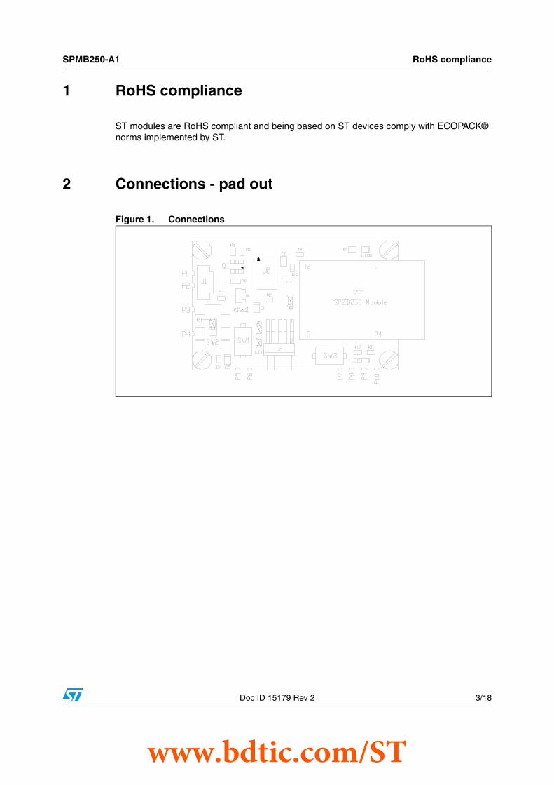
2 Connections - pad out
Figure 1. Connections
www.bdtic.com/ST
Block diagram SPMB250-A1
4/18 Doc ID 15179 Rev 2
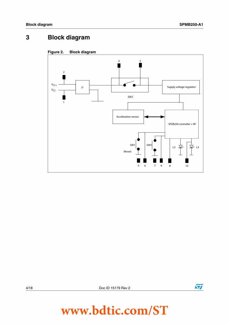
3 Block diagram
Figure 2. Block diagram
www.bdtic.com/ST
SPMB250-A1 Maximum ratings
Doc ID 15179 Rev 2 5/18
4 Maximum ratings
4.1 Absolute maximum ratings
4.2 Operating rangesOperating ranges define the limits for functional operation and parametric characteristics of the module.
Functionality outside these limits is not implied
Table 1. Absolute maximum ratings
Symbol Parameter Values
Unit Min Max
VCC Board supply voltage 7 V
TOPmax Operating ambient temperature -40 +85 °C
TSTG Storage temperature -40 +85 °C
Table 2. Operating ranges
Symbol Parameter ConditionsValues
UnitMin Typ Max
VCC Module supply voltage -40 °C < T < 85 °C 3.6 6 V
TSTGOperating ambient temperature
-40 +85 °C
IOP Operation current (1)
1. Values indicated in the table are referred to the single states (Standby TX,RX,…); the overall current depends on the working strategy used by the application
Vin = 4 V stand by 16 μA
Vin = 4 V TX mode 37 mA
Vin = 4 V RX mode 36 mA
Vin = 4 V CPU only 9 mA
www.bdtic.com/ST
Electrical characteristics SPMB250-A1
6/18 Doc ID 15179 Rev 2
5 Electrical characteristics
5.1 DC I/O specification Table 3. DC input / output specification
Symbol Parameter ConditionsValues
UnitMin Typ Max
VILLow level input voltage SW1 (Reset) and SW3
Vin = 4 V 0.6 V
VOLLow level output voltageP8 (L1) and P10 (L2)
Vin = 4 V 0.2 V
VOHHigh level output voltageP8 (L1) and P10 (L2)
Vin = 4 V 2.7 3.3 V
IOLed Vin = 4 V 4 mA
RFin Input frequency range 2405 2480 MHz
RX sens Receiver sensitivity @PER 1 % -92 dBm
RFout Output frequency range 2405 2480 MHz
TXpout Nominal output power @ 2402 – 2480 MHz 0 dBm
FSAcceleration sensor Measurement Range
±1.7 ±2.0 g
±5.3 ±6.0 g
DresAcceleration sensorResolution
Full-scale = ±2 gOutput data rate = 40 Hz
1.0 mg
SoAcceleration sensorSensitivity
Full-scale = ±2 g12 bit representation
920 1024 1126 LSb/g
Full-scale = ±6 g12 bit representation
306 340 374 LSB/g
www.bdtic.com/ST
SPMB250-A1 Board description
Doc ID 15179 Rev 2 7/18
6 Board description
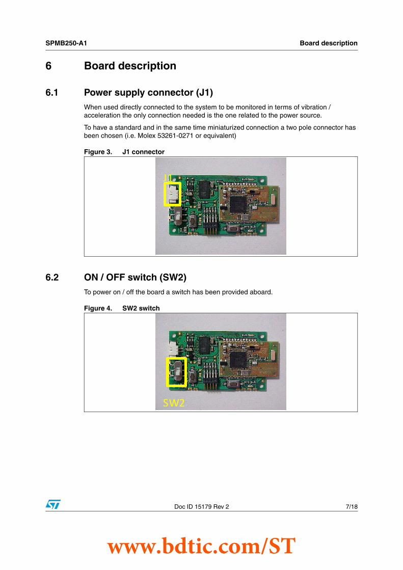
6.1 Power supply connector (J1)When used directly connected to the system to be monitored in terms of vibration / acceleration the only connection needed is the one related to the power source.
To have a standard and in the same time miniaturized connection a two pole connector has been chosen (i.e. Molex 53261-0271 or equivalent)
Figure 3. J1 connector
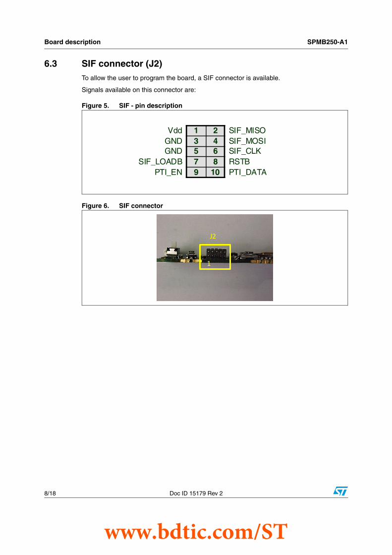
6.2 ON / OFF switch (SW2)To power on / off the board a switch has been provided aboard.
Figure 4. SW2 switch
J1
SW2
www.bdtic.com/ST
Board description SPMB250-A1
8/18 Doc ID 15179 Rev 2
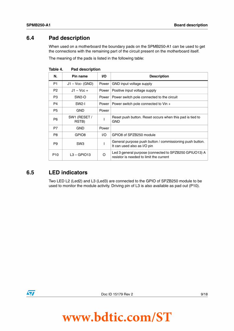
6.3 SIF connector (J2) To allow the user to program the board, a SIF connector is available.
Signals available on this connector are:
Figure 5. SIF - pin description
Figure 6. SIF connector
Vdd 1 2 SIF_MISOGND 3 4 SIF_MOSIGND 5 6 SIF_CLK
SIF_LOADB 7 8 RSTBPTI_EN 9 10 PTI_DATA
J2
1
www.bdtic.com/ST
SPMB250-A1 Board description
Doc ID 15179 Rev 2 9/18
6.4 Pad descriptionWhen used on a motherboard the boundary pads on the SPMB250-A1 can be used to get the connections with the remaining part of the circuit present on the motherboard itself.
The meaning of the pads is listed in the following table:
6.5 LED indicatorsTwo LED L2 (Led2) and L3 (Led3) are connected to the GPIO of SPZB250 module to be used to monitor the module activity. Driving pin of L3 is also available as pad out (P10).
Table 4. Pad description
N. Pin name I/O Description
P1 J1 – Vcc- (GND) Power GND input voltage supply
P2 J1 – Vcc + Power Positive input voltage supply
P3 SW2-O Power Power switch pole connected to the circuit
P4 SW2-I Power Power switch pole connected to Vin +
P5 GND Power
P6 SW1 (RESET /
RSTB)I
Reset push button. Reset occurs when this pad is tied to GND
P7 GND Power
P8 GPIO8 I/O GPIO8 of SPZB250 module
P9 SW3 IGeneral purpose push button / commissioning push button. It can used also as I/O pin
P10 L3 – GPIO13 OLed 3 general purpose (connected to SPZB250 GPIUO13) A resistor is needed to limit the current
www.bdtic.com/ST
Board layout SPMB250-A1
10/18 Doc ID 15179 Rev 2
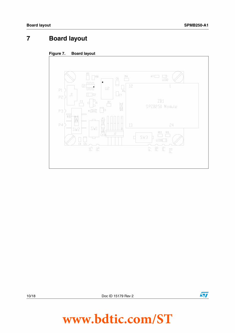
7 Board layout
Figure 7. Board layout
www.bdtic.com/ST
SPMB250-A1 Soldering
Doc ID 15179 Rev 2 11/18
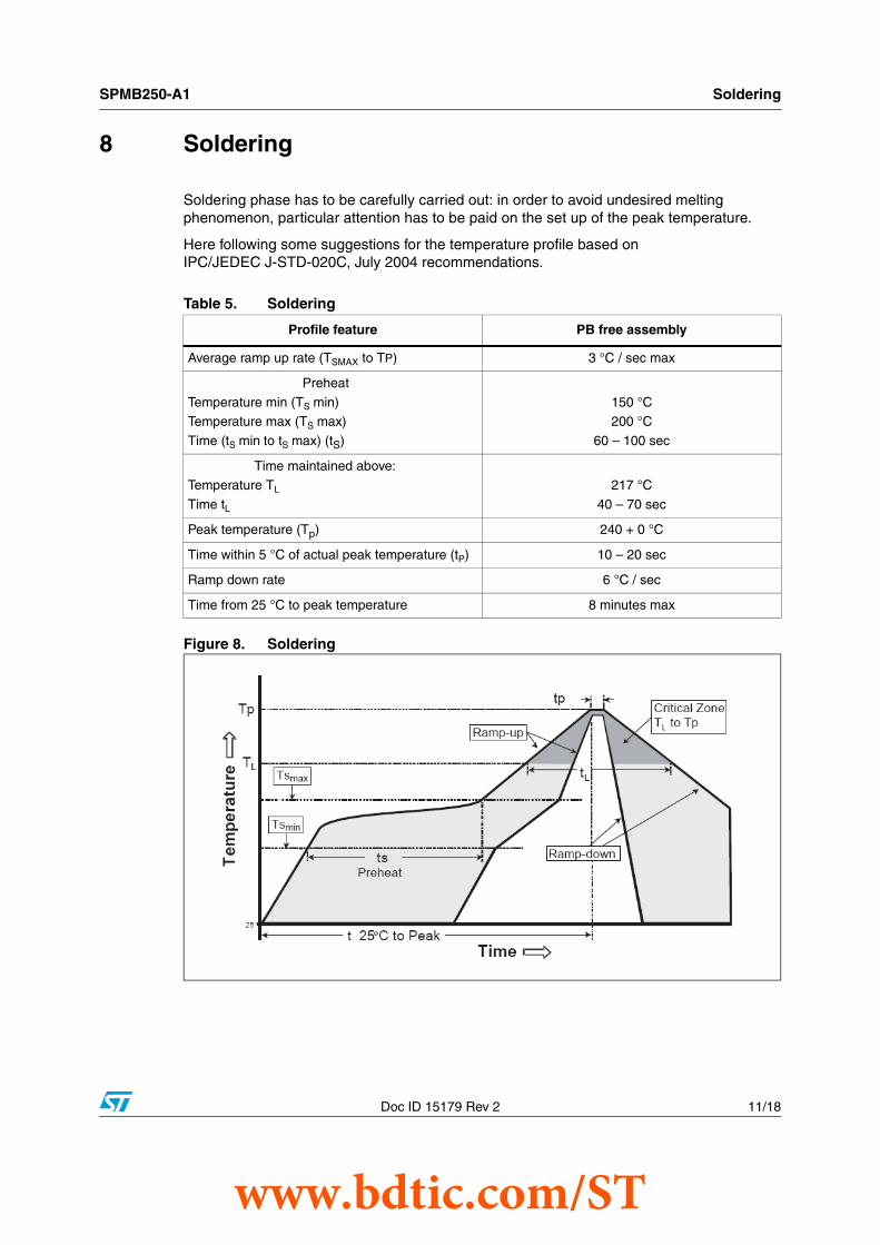
8 Soldering
Soldering phase has to be carefully carried out: in order to avoid undesired melting phenomenon, particular attention has to be paid on the set up of the peak temperature.
Here following some suggestions for the temperature profile based onIPC/JEDEC J-STD-020C, July 2004 recommendations.
Figure 8. Soldering
Table 5. Soldering
Profile feature PB free assembly
Average ramp up rate (TSMAX to TP) 3 °C / sec max
Preheat
Temperature min (TS min)Temperature max (TS max)
Time (tS min to tS max) (tS)
150 °C200 °C
60 – 100 sec
Time maintained above:Temperature TL
Time tL
217 °C
40 – 70 sec
Peak temperature (Tp) 240 + 0 °C
Time within 5 °C of actual peak temperature (tP) 10 – 20 sec
Ramp down rate 6 °C / sec
Time from 25 °C to peak temperature 8 minutes max
www.bdtic.com/ST
Recommendations SPMB250-A1
12/18 Doc ID 15179 Rev 2
9 Recommendations
● An integrated antenna is present on the board:
– Assembly the board in the application avoiding any shielding of the antenna
– Avoid metallic parts close to the antenna
– Do not use metallic case
● Board fixing can be done with 4 screws:
– In case of fixing on metallic base insert an insulator foil between the board and the base in order to avoid any potential short circuit
www.bdtic.com/ST
SPMB250-A1 Radiation pattern
Doc ID 15179 Rev 2 13/18
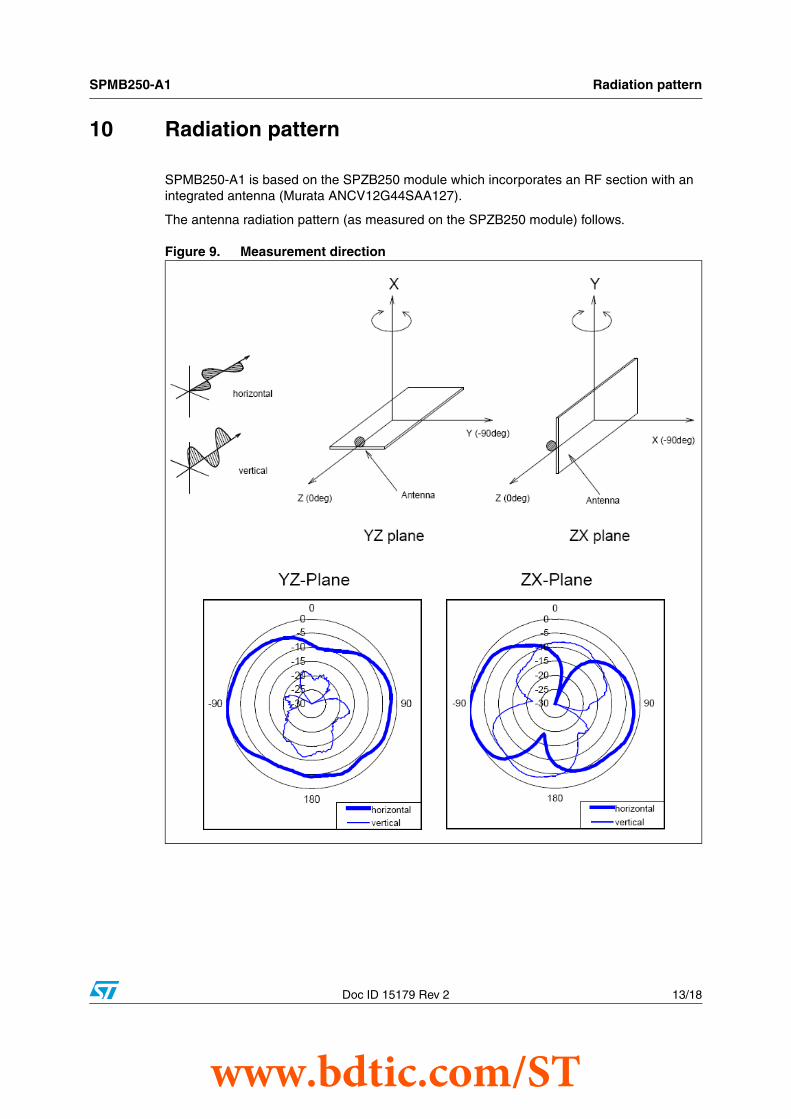
10 Radiation pattern
SPMB250-A1 is based on the SPZB250 module which incorporates an RF section with an integrated antenna (Murata ANCV12G44SAA127).
The antenna radiation pattern (as measured on the SPZB250 module) follows.
Figure 9. Measurement direction
www.bdtic.com/ST
Mechanical dimensions SPMB250-A1
14/18 Doc ID 15179 Rev 2
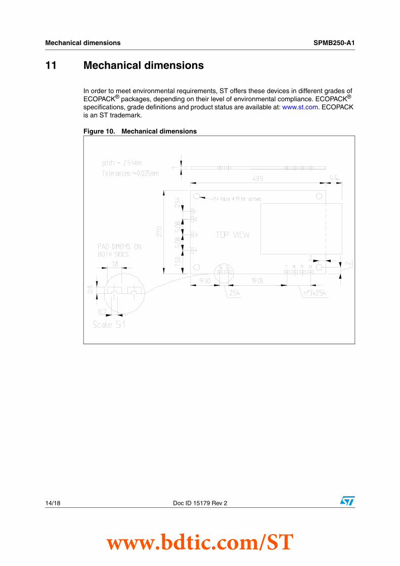
11 Mechanical dimensions
In order to meet environmental requirements, ST offers these devices in different grades of ECOPACK® packages, depending on their level of environmental compliance. ECOPACK® specifications, grade definitions and product status are available at: www.st.com. ECOPACK is an ST trademark.
Figure 10. Mechanical dimensions
www.bdtic.com/ST
SPMB250-A1 Mechanical dimensions
Doc ID 15179 Rev 2 15/18
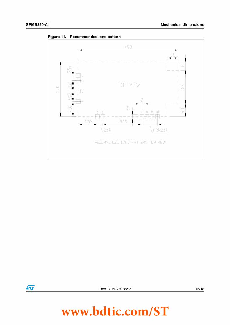
Figure 11. Recommended land pattern
www.bdtic.com/ST
Ordering information scheme SPMB250-A1
16/18 Doc ID 15179 Rev 2
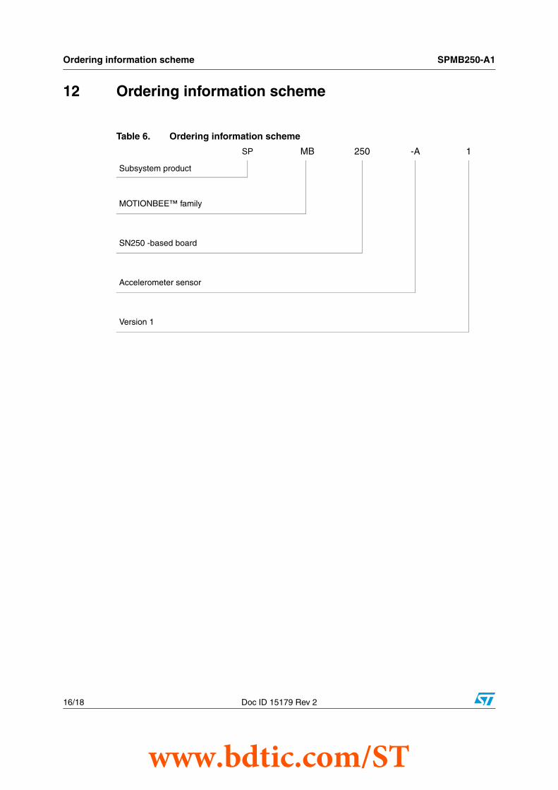
12 Ordering information scheme
Table 6. Ordering information scheme
SP MB 250 -A 1
Subsystem product
MOTIONBEE™ family
SN250 -based board
Accelerometer sensor
Version 1
www.bdtic.com/ST
SPMB250-A1 Revision history
Doc ID 15179 Rev 2 17/18
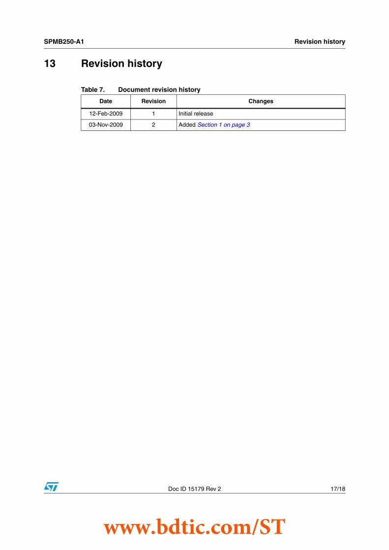
13 Revision history
Table 7. Document revision history
Date Revision Changes
12-Feb-2009 1 Initial release
03-Nov-2009 2 Added Section 1 on page 3
www.bdtic.com/ST
SPMB250-A1
18/18 Doc ID 15179 Rev 2
Please Read Carefully:
Information in this document is provided solely in connection with ST products. STMicroelectronics NV and its subsidiaries (“ST”) reserve theright to make changes, corrections, modifications or improvements, to this document, and the products and services described herein at anytime, without notice.
All ST products are sold pursuant to ST’s terms and conditions of sale.
Purchasers are solely responsible for the choice, selection and use of the ST products and services described herein, and ST assumes noliability whatsoever relating to the choice, selection or use of the ST products and services described herein.
No license, express or implied, by estoppel or otherwise, to any intellectual property rights is granted under this document. If any part of thisdocument refers to any third party products or services it shall not be deemed a license grant by ST for the use of such third party productsor services, or any intellectual property contained therein or considered as a warranty covering the use in any manner whatsoever of suchthird party products or services or any intellectual property contained therein.
UNLESS OTHERWISE SET FORTH IN ST’S TERMS AND CONDITIONS OF SALE ST DISCLAIMS ANY EXPRESS OR IMPLIEDWARRANTY WITH RESPECT TO THE USE AND/OR SALE OF ST PRODUCTS INCLUDING WITHOUT LIMITATION IMPLIEDWARRANTIES OF MERCHANTABILITY, FITNESS FOR A PARTICULAR PURPOSE (AND THEIR EQUIVALENTS UNDER THE LAWSOF ANY JURISDICTION), OR INFRINGEMENT OF ANY PATENT, COPYRIGHT OR OTHER INTELLECTUAL PROPERTY RIGHT.
UNLESS EXPRESSLY APPROVED IN WRITING BY AN AUTHORIZED ST REPRESENTATIVE, ST PRODUCTS ARE NOTRECOMMENDED, AUTHORIZED OR WARRANTED FOR USE IN MILITARY, AIR CRAFT, SPACE, LIFE SAVING, OR LIFE SUSTAININGAPPLICATIONS, NOR IN PRODUCTS OR SYSTEMS WHERE FAILURE OR MALFUNCTION MAY RESULT IN PERSONAL INJURY,DEATH, OR SEVERE PROPERTY OR ENVIRONMENTAL DAMAGE. ST PRODUCTS WHICH ARE NOT SPECIFIED AS "AUTOMOTIVEGRADE" MAY ONLY BE USED IN AUTOMOTIVE APPLICATIONS AT USER’S OWN RISK.
Resale of ST products with provisions different from the statements and/or technical features set forth in this document shall immediately voidany warranty granted by ST for the ST product or service described herein and shall not create or extend in any manner whatsoever, anyliability of ST.
ST and the ST logo are trademarks or registered trademarks of ST in various countries.
Information in this document supersedes and replaces all information previously supplied.
The ST logo is a registered trademark of STMicroelectronics. All other names are the property of their respective owners.
© 2009 STMicroelectronics - All rights reserved
STMicroelectronics group of companies
Australia - Belgium - Brazil - Canada - China - Czech Republic - Finland - France - Germany - Hong Kong - India - Israel - Italy - Japan - Malaysia - Malta - Morocco - Philippines - Singapore - Spain - Sweden - Switzerland - United Kingdom - United States of America
www.st.com
www.bdtic.com/ST