Embed Size (px)
Citation preview

MP4816A 16-Channel, High-Voltage Analog Switch
with Output Bleed Resistors
MP4816A Rev. 1.02 www.MonolithicPower.com 1 7/6/2020 MPS Proprietary Information. Patent Protected. Unauthorized Photocopy and Duplication Prohibited. © 2020 MPS. All Rights Reserved.
DESCRIPTION The MP4816A is a 16-channel, high-voltage, single-pole, single-throw, SPST, analog switch with integrated output bleed resistors designed for medical ultrasound imaging applications. The MP4816A is designed to multiplex transmit and receive voltages to and from multiple piezoelectric transducers (PZT).
The output switches are controlled by a 16-bit serial shift register followed by a 16-bit data latch. A data out pin (DOUT) is provided to allow for multiple devices to be cascaded together. This helps minimize the number of input/output (I/O) control lines. A logic high in the data latch turns on the corresponding analog switch. A logic low turns off the corresponding analog switch.
The MP4816A does not require any high-voltage supplies. Only two low-voltage supplies are required (3.3V and 10V). The analog switch can block or pass analog voltages up to ±90V with peak currents of up to ±2.0A.
The MP4816A is available in a TQFP-48 (7mmx7mm) package.
FEATURES
No High-Voltage Supplies Required
16 Channels
Up to ±90V Analog Signals
12.5Ω Typical Switch Resistance
±2.0A Typical Switch Peak Current
Off-Isolation of -66dB at 5.0MHz
Integrated Output Bleed Resistor
80MHz Clock Frequency
Available in a TQFP-48 (7mmx7mm) Package
APPLICATIONS
Medical Ultrasound Imaging
Non-Destructive Testing (NDT)
All MPS parts are lead-free, halogen-free, and adhere to the RoHS directive. For MPS green status, please visit the MPS website under Quality Assurance. “MPS” and “The Future of Analog IC Technology” are registered trademarks of Monolithic Power Systems, Inc.
TYPICAL APPLICATION
Tx
RxT/R
SW
Tx-0 SWin-0 PZT-0
SWin-1 PZT-64
SWin-2 PZT-128
Tx
RxT/R
SW
Tx-63 SWin-189 PZT- 63
SWin-190 PZT-127
SWin-191 PZT-191
SWout-0
SWout-1
SWout-2
SWout-189
SWout-190
SWout-191

MP4816A – 16-CHANNEL HIGH VOLTAGE ANALOG SWITCH W/ OUTPUT BLEED RESISTORS
MP4816A Rev. 1.02 www.MonolithicPower.com 2 7/6/2020 MPS Proprietary Information. Patent Protected. Unauthorized Photocopy and Duplication Prohibited. © 2020 MPS. All Rights Reserved.
ORDERING INFORMATION
Part Number Package Top Marking
MP4816AGFP TQFP-48 (7mmx7mm) See Below
TOP MARKING
MPS: MPS prefix YY: Year code WW: Week code MP4816A: Product code of MP4816AGFP LLLLLLLLL: Lot number
PACKAGE REFERENCE
TOP VIEW
1
2
3
4
5
6
7
8
9
10
11
12
NC
NC
SWout-4
SWin-4
SWout-3
SWin-3
SWout-2
SWin-2
SWout-1
SWin-1
SWout-0
SWin-0
13
14
15
16
17
18
19
20
21
22
23
24
36
35
34
33
32
31
30
29
28
27
26
25
48
47
46
45
44
43
42
41
40
39
38
37
Gn
d
Gn
d
VD
D
NC
Gn
d
VL
L
DIN
Clk
LE
\
Clr
DO
UT
RG
nd
SWout-15
NC
NC
SW
ou
t-1
0
SWin-15
SWout-14
SWin-14
SWout-13
SWin-13
SWout-12
SWin-12
SWout-11
SWin-11
SW
in-1
0
SW
ou
t-9
SW
ou
t-8
SW
ou
t-7
SW
ou
t-6
SW
ou
t-5
SW
in-9
SW
in-8
SW
in-7
SW
in-6
SW
in-5
TQFP-48 (7mmx7mm)

MP4816A – 16-CHANNEL HIGH VOLTAGE ANALOG SWITCH W/ OUTPUT BLEED RESISTORS
MP4816A Rev. 1.02 www.MonolithicPower.com 3 7/6/2020 MPS Proprietary Information. Patent Protected. Unauthorized Photocopy and Duplication Prohibited. © 2020 MPS. All Rights Reserved.
ABSOLUTE MAXIMUM RATINGS (1) Logic supply (VLL) ......................... -0.5V to +6.6V Translator supply (VDD) ................. -0.5V to +11V Analog signal range (pulsed voltage) (VSIG) ........ ........................................................ 0V to ±105V Junction temperature ................................ 150°C Lead temperature ..................................... 260°C Continuous power dissipation (TA = 25°C) (2)
................................................................. 1.47W HBM: SWoutx: Class 1B, SWinx: Class 1C: Other pins: Class 2 (JEDEC Standard) CDM: All pins: Class C3 (JEDEC standard) Storage temperature .................. -55°C to 150°C
Recommended Operating Conditions (3)
Logic supply voltage (VLL) ............... 2.7V to 5.5V Translator supply voltage (VDD) ........... 9V to 10V Analog signal range (VSIG) .................. 0 to ±90V Junction temperature (TJ) ........ -25°C to +125°C
Thermal Resistance (4) θJA θJC TQFP-48 (7mmx7mm) ........... 68 ....... 15 ... °C/W
NOTES: 1) Exceeding these ratings may damage the device. 2) The maximum allowable power dissipation is a function of the
maximum junction temperature TJ (MAX), the junction-to-ambient thermal resistance θJA, and the ambient temperature TA. The maximum allowable continuous power dissipation at any ambient temperature is calculated by PD (MAX) = (TJ
(MAX)-TA)/θJA. Exceeding the maximum allowable power dissipation produces an excessive die temperature, resulting in permanent damage.
3) The device is not guaranteed to function outside of its operating conditions.
4) Measured on JESD51-7, 4-layer PCB.

MP4816A – 16-CHANNEL HIGH VOLTAGE ANALOG SWITCH W/ OUTPUT BLEED RESISTORS
MP4816A Rev. 1.02 www.MonolithicPower.com 4 7/6/2020 MPS Proprietary Information. Patent Protected. Unauthorized Photocopy and Duplication Prohibited. © 2020 MPS. All Rights Reserved.
DC ELECTRICAL CHARACTERISTICS VDD = 10V, VLL = 5V, unless otherwise noted. (5)
Parameter Sym Conditions TJ = 0°C TJ = 25°C TJ = 70°C
Units Min Max Min Typ Max Min Max
Analog signal range VSIG Applied to SWin pin 0 ±90 0 ±90 0 ±90 V
On resistance RON
ISIG = ±5.0mA, SWout = 0V. See test circuit 1.
16 12.5 19 24
Ω ISIG = ±200mA, SWout = 0V. See test circuit 1.
16 12.5 19 24
Small signal on resistance matching
∆RON ISIG = ±5.0mA, Swout = 0V
- 5.0 - - %
Large signal on resistance (6)
RONL
ISIG = ±1.0A, tPW ≤ 500ns, duty cycle ≤ 1.0%, SWout = 0V. See test circuit 2.
13 Ω
Switch output peak current (6)
ISWPK tPW < 100ns, duty cycle < 1.0%
±2.0 A
Output bleed resistor RBLEED ISIG = ±50µA 20 50 20 30 50 20 50 kΩ
Switch off DC offset VDC-OFF No load, no VSIG. See test circuit 3.
±50 ±50 ±50 mV
Switch on DC offset VDC-ON No load, no VSIG. See test circuit 3.
±50 ±50 ±50 mV
VLL quiescent current ILLQ All logic inputs are static 50 50 50 µA
VDD quiescent current IDDQ All switches on or off, SWin = SWout = ground
60 60 60 µA
VLL average dynamic current
ILL
fCLK = 40MHz, DIN = 20MHz, LE\ = H, Clr = L
2.2 6
mA fCLK = 80MHz, DIN = 40MHz, LE\ = H, Clr = L (6)
4.3
VDD average dynamic current
IDD All output switches are turning on and off at 50kHz
2.3 4 mA
Input voltage logic low VIL 0 0.2VLL 0 0.2VLL 0 0.2VLL V
Input voltage logic high VIH 0.8VLL VLL 0.8VLL VLL 0.8VLL VLL V
Input current logic low IIL -1.0 -1.0 -1.0 µA
Input current logic high IIH 1.0 1.0 1.0 µA
Data out logic low voltage
VOL Isink = 10mA 1.0 1.0 1.0 V
Data out logic high voltage
VOH Isource = 10mA VLL-1.0
VLL-1.0
VLL-1.0
V
Logic input capacitance (6)
CIN 10 10 10 pF
NOTES: 5) Production test is at 25°C only. 0°C and 70°C limits are guaranteed by design and characterization. 6) Parameters are not tested in mass production, only guaranteed by design or bench characterization.

MP4816A – 16-CHANNEL HIGH VOLTAGE ANALOG SWITCH W/ OUTPUT BLEED RESISTORS
MP4816A Rev. 1.02 www.MonolithicPower.com 5 7/6/2020 MPS Proprietary Information. Patent Protected. Unauthorized Photocopy and Duplication Prohibited. © 2020 MPS. All Rights Reserved.
AC ELECTRICAL CHARACTERISTICS VDD = 10V, VLL = 5Vunless otherwise noted. (5)
Parameter Sym Conditions TJ = 0°C TJ = 25°C TJ = 70°C
Units Min Max Min Typ Max Min Max
Clock frequency (6) fCLK 50% duty cycle 80 0 80 0 80 MHz
Clock rise time (6) tr 50 50 50 ns
Clock fall time (6) tf 50 50 50 ns
Set-up time from data to rising edge of clock (6)
tSU 3.0 3.0 3.0 ns
Hold time from rising edge of clock to data (6)
tH 3.0 3.0 3.0 ns
Set-up time before LE\ rises (6)
tSD 6.0 6.0 6.0 ns
LE\ pulse width (6) tWLE bar 6.0 6.0 6.0 ns
Clear pulse width (6) tWCLR 6.0 6.0 6.0 ns
Data out propagation delay time from rising edge of clock (6)
tDOLH,
tDOHL 20pF on DOUT to ground 4.0 8.0 4.0 6.0 8.0 4.0 8.0 ns
Output switch turn on time
TON SWin = 2.0V, SWout = 50Ω to ground. See test circuit 4.
2.0 2.0 2.0 µs
Output switch turn off time
TOFF 2.0 2.0 2.0 µs
Analog signal slew rate (6)
dv/dt 20 20 20 V/ns
Off isolation (6) KO freq = 5.0MHz, Rload = 50Ω. See test circuit 5.
-66 dB
Switch crosstalk (6) KCR freq = 5.0MHz, Rload = 50Ω. See test circuit 6.
-60 dB
Switch off capacitance (6)
CSWin-
OFF 10 pF
Switch on capacitance (6)
CSW-ON 13 pF
Positive output voltage spike (6)
+VSPK SWin = 1kΩ to ground, SWout = 50Ω to ground. See test circuit 7.
16 mV
Negative output voltage spike (6)
-VSPK -14 mV
Output charge injection (6)
QINJ Cload = 1000pF. See test circuit 8.
18 pC
NOTES: 5) Production test is at 25°C only. 0°C and 70°C limits are guaranteed by design and characterization. 6) Parameters are not tested in mass production, only guaranteed by design or bench characterization.

MP4816A – 16-CHANNEL HIGH VOLTAGE ANALOG SWITCH W/ OUTPUT BLEED RESISTORS
MP4816A Rev. 1.02 www.MonolithicPower.com 6 7/6/2020 MPS Proprietary Information. Patent Protected. Unauthorized Photocopy and Duplication Prohibited. © 2020 MPS. All Rights Reserved.
PIN FUNCTIONS
Package Pin #
Name Description
1, 2, 16, 35, 36
NC No internal connections.
3 SWout-4 Analog switch output 4. Connect SWout-4 to the piezoelectric transducer.
4 SWin-4 Analog switch input 4. Connect SWin-4 to the high-voltage pulser/transmitter.
5 SWout-3 Analog switch output 3. Connect SWout-3 to the piezoelectric transducer.
6 SWin-3 Analog switch input 3. Connect SWin-3 to the high-voltage pulser/transmitter.
7 SWout-2 Analog switch output 2. Connect SWout-2 to the piezoelectric transducer.
8 SWin-2 Analog switch input 2. Connect SWin-2 to the high-voltage pulser/transmitter.
9 SWout-1 Analog switch output 1. Connect SWout-1 to the piezoelectric transducer.
10 SWin-1 Analog switch input 1. Connect SWin-1 to the high-voltage pulser/transmitter.
11 SWout-0 Analog switch output 0. Connect SWout-0 to the piezoelectric transducer.
12 SWin-0 Analog switch input 0. Connect SWin-0 to the high-voltage pulser/transmitter.
13, 14, 17
GND Device ground.
15 VDD Translators supply voltage. VDD has a 9 - 10V operating range.
18 VLL Logic supply voltage. VLL has a 2.7 - 5.5V operating range.
19 DIN Logic input. DIN is the data input for the 16-bit serial shift register.
20 Clk Logic input. Clk is the clock input for the 16-bit serial shift register. Data is loaded into Clk during the rising edge of the clock.
21 LE\ Logic input. LE\ is the latch enable bar for the 16-bit latch. Logic low on LE\ transfers data from the shift registers to the latches. Logic high on LE\ holds the data in the latches. Refer to the logic truth table on page 9.
22 Clr Logic input. Clr is the clear input for the 16-bit latch. Logic high on Clr clears the data in the latches by setting them all to 0. Data in the shift register remains unchanged. Refer to the logic truth table on page 9.
23 DOUT Logic output. DOUT is the data output for the 16-bit serial shift register.
24 RGND Output bleed resistor ground path.
25 SWout-15 Analog switch output 15. Connect SWout-15 to the piezoelectric transducer.
26 SWin-15 Analog switch input 15. Connect SWin-15 to the high-voltage pulser/transmitter.
27 SWout-14 Analog switch output 14. Connect SWout-14 to the piezoelectric transducer.
28 SWin-14 Analog switch input 14. Connect SWin-14 to the high-voltage pulser/transmitter.
29 SWout-13 Analog switch output 13. Connect SWout-13to the piezoelectric transducer.
30 SWin-13 Analog switch input 13. Connect SWin-13 to the high-voltage pulser/transmitter.
31 SWout-12 Analog switch output 12. Connect SWout-12 to the piezoelectric transducer.
32 SWin-12 Analog switch input 12. Connect SWin-12 to the high-voltage pulser/transmitter.

MP4816A – 16-CHANNEL HIGH VOLTAGE ANALOG SWITCH W/ OUTPUT BLEED RESISTORS
MP4816A Rev. 1.02 www.MonolithicPower.com 7 7/6/2020 MPS Proprietary Information. Patent Protected. Unauthorized Photocopy and Duplication Prohibited. © 2020 MPS. All Rights Reserved.
PIN FUNCTIONS (continued)
Package Pin #
Name Description
33 SWout-11 Analog switch output 11. Connect SWout-11 to the piezoelectric transducer.
34 SWin-11 Analog switch input 11. Connect SWin-11 to the high-voltage pulser/transmitter.
37 SWout-10 Analog switch output 10. Connect SWout-10 to the piezoelectric transducer.
38 SWin-10 Analog switch input 10. Connect SWin-10 to the high-voltage pulser/transmitter.
39 SWout-9 Analog switch output 9. Connect SWout-9 to the piezoelectric transducer.
40 SWin-9 Analog switch input 9. Connect SWin-9 to the high-voltage pulser/transmitter.
41 SWout-8 Analog switch output 8. Connect SWout-8 to the piezoelectric transducer.
42 SWin-8 Analog switch input 8. Connect SWin-8 to the high-voltage pulser/transmitter.
43 SWout-7 Analog switch output 7. Connect SWout-7 to the piezoelectric transducer.
44 SWin-7 Analog switch input 7. Connect SWin-7 to the high-voltage pulser/transmitter.
45 SWout-6 Analog switch output 6. Connect SWout-6 to the piezoelectric transducer.
46 SWin-6 Analog switch input 6. Connect SWin-6 to the high-voltage pulser/transmitter.
47 SWout-5 Analog switch output 5. Connect SWout-5 to the piezoelectric transducer.
48 SWin-5 Analog switch input 5. Connect SWin-5 to the high-voltage pulser/transmitter.

MP4816A – 16-CHANNEL HIGH VOLTAGE ANALOG SWITCH W/ OUTPUT BLEED RESISTORS
MP4816A Rev. 1.02 www.MonolithicPower.com 8 7/6/2020 MPS Proprietary Information. Patent Protected. Unauthorized Photocopy and Duplication Prohibited. © 2020 MPS. All Rights Reserved.
TYPICAL PERFORMANCE CHARACTERISTICS
Bandwidth vs. Frequency RLOAD = 50Ω
Off-Isolation vs. Frequency RLOAD = 50Ω
Switch Resistance vs. Switch Input
Voltage RLOAD = 50Ω
ILL vs. Clock Frequency VLL = 5.0V, VDD = 10V
IDD vs. Switch On/Off Frequency
VLL = 5.0V, VDD = 10V, all 16 channels switching
ILL Current vs. VLL Voltage Clk = 40MHz, DIN = 20MHz
-8
-7
-6
-5
-4
-3
-2
-1
0
1 10 100
BA
ND
WID
TH
(dB
)
FREQUENCY ( MHz )
-90
-80
-70
-60
-50
-40
1.0 10.0 100.0
OFF-I
SO
LA
TIO
N(d
B)
FREQUENCY ( MHz )
0
2
4
6
8
10
12
14
16
-90 -70 -50 -30 -10 10 30 50 70 90
RO
N(
Ω)
VSWIN ( V )
0.00
1.00
2.00
3.00
4.00
5.00
0 10 20 30 40 50 60 70 80
I LL
( m
A )
CLK FREQ ( MHz )
0.0
0.5
1.0
1.5
2.0
2.5
3.0
0 5 10 15 20 25 30 35 40 45 50
I DD
( m
A )
SWITCH ON/OFF FREQ ( kHz )
0
1
2
3
4
5
2.7 3.1 3.5 3.9 4.3 4.7 5.1 5.5
I LL
CU
RR
EN
T
( m
A )
VLL ( V )

MP4816A – 16-CHANNEL HIGH VOLTAGE ANALOG SWITCH W/ OUTPUT BLEED RESISTORS
MP4816A Rev. 1.02 www.MonolithicPower.com 9 7/6/2020 MPS Proprietary Information. Patent Protected. Unauthorized Photocopy and Duplication Prohibited. © 2020 MPS. All Rights Reserved.
TIMING DIAGRAM
Clk
tSU tH
DIN
DOUT
tDO
tWLE
50% 50%
50%
tSD
50% 50%
DN DN+1DN-1
50%
50%
LE\
tON
10%
tOFF
Clr
VOUT
tWCLR
50% 50%
90%
ON
OFF
LOGIC TRUTH TABLE
Logic Input Switch State
D0 D1 D2 D15 LE bar Clr SW0 SW1 SW2 SW15
L - - - L L Off - - -
H - - - L L On - - -
- L - - L L - Off - -
- H - - L L - On - -
- - L - L L - - Off -
- - H - L L - - On -
- - - L L L - - - Off
- - - H L L - - - On
x x x x H L Holds previous state
x x x x x H All switches off
L = logic level low H = logic level high x = value does not matter
MP4816A – 16-CHANNEL HIGH VOLTAGE ANALOG SWITCH W/ OUTPUT BLEED RESISTORS
MP4816A Rev. 1.02 www.MonolithicPower.com 10 7/6/2020 MPS Proprietary Information. Patent Protected. Unauthorized Photocopy and Duplication Prohibited. © 2020 MPS. All Rights Reserved.
TEST CIRCUITS Test Circuit 1
VLL
ISIG = ±5.0mA to ±200mA
Gnd
VDD
ISIG
Ron
SWoutSWin
RGnd
RON = ISIG
VSWin
VSWin
Test Circuit 2
VLL
ISIG = 0 to ±1.0A
tPW ≤ 500ns
Duty cycle ≤ 1.0%
Gnd
VDD
ISIG
Large Signal Ron
SWoutSWin
RGnd
RONL = ISIG
VSWin
Test Circuit 3
VLL
Gnd
VDD
Vout
Switch On/Off DC Offset
SWoutSWin
RGnd
MP4816A – 16-CHANNEL HIGH VOLTAGE ANALOG SWITCH W/ OUTPUT BLEED RESISTORS
MP4816A Rev. 1.02 www.MonolithicPower.com 11 7/6/2020 MPS Proprietary Information. Patent Protected. Unauthorized Photocopy and Duplication Prohibited. © 2020 MPS. All Rights Reserved.
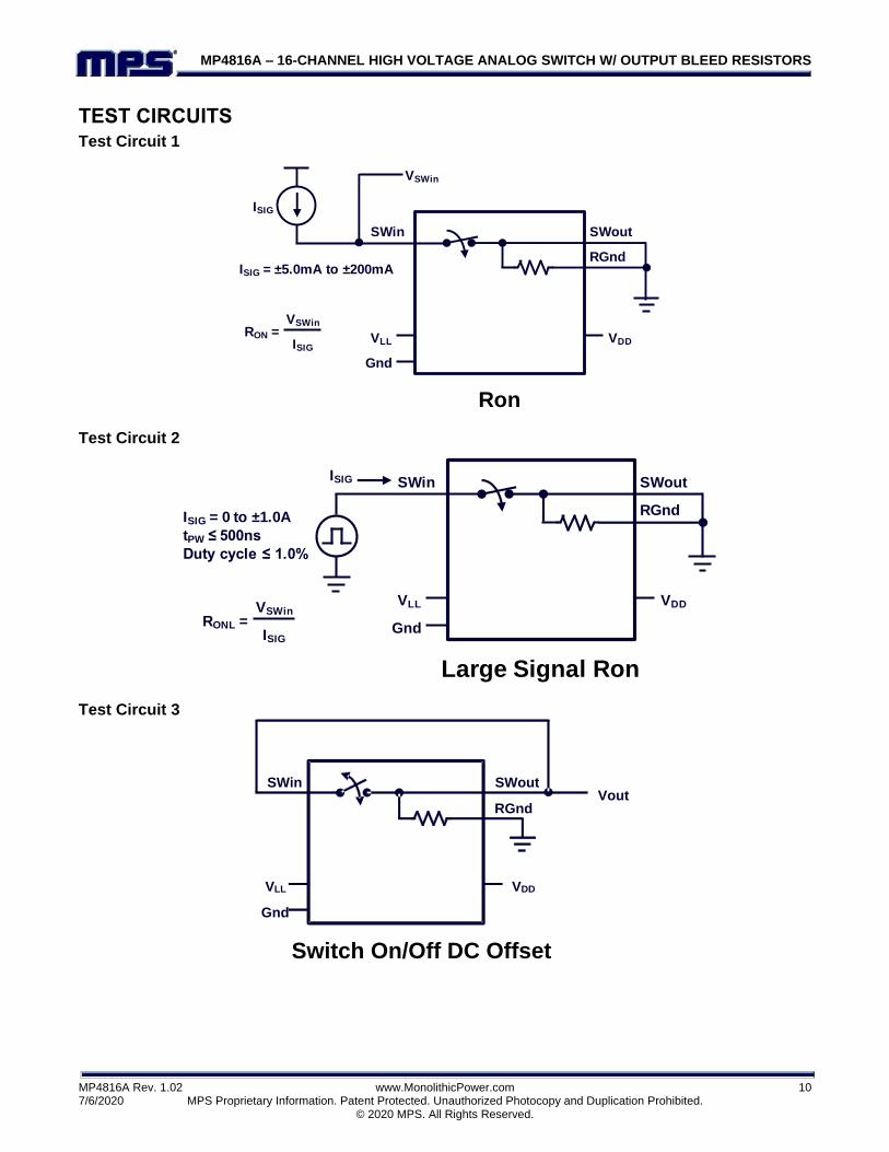
TEST CIRCUITS (continued) Test Circuit 4
90%
TON
10%
TOFF
VLL
Gnd
VDD
SWout
TON / TOFF
SWinVout
RGnd
2.0V
Din
Clk
Vout
Din
Clk
50Ω
Test Circuit 5
VLL
VSIG=10Vp-p
@5.0MHz
Sine wave
Gnd
VDD
Vout
50W
KO = 20LogVout
VSIG
Switch Off-Isolation
SWoutSWin
RGnd
Test Circuit 6
VLL
VSIG=10Vp-p
@5.0MHz
Sine wave
Gnd
VDD
VoutNC
50W
50W
KCR = 20LogVout
VSIG
Switch Crosstalk
SWout
SWin
RGnd
MP4816A – 16-CHANNEL HIGH VOLTAGE ANALOG SWITCH W/ OUTPUT BLEED RESISTORS
MP4816A Rev. 1.02 www.MonolithicPower.com 12 7/6/2020 MPS Proprietary Information. Patent Protected. Unauthorized Photocopy and Duplication Prohibited. © 2020 MPS. All Rights Reserved.
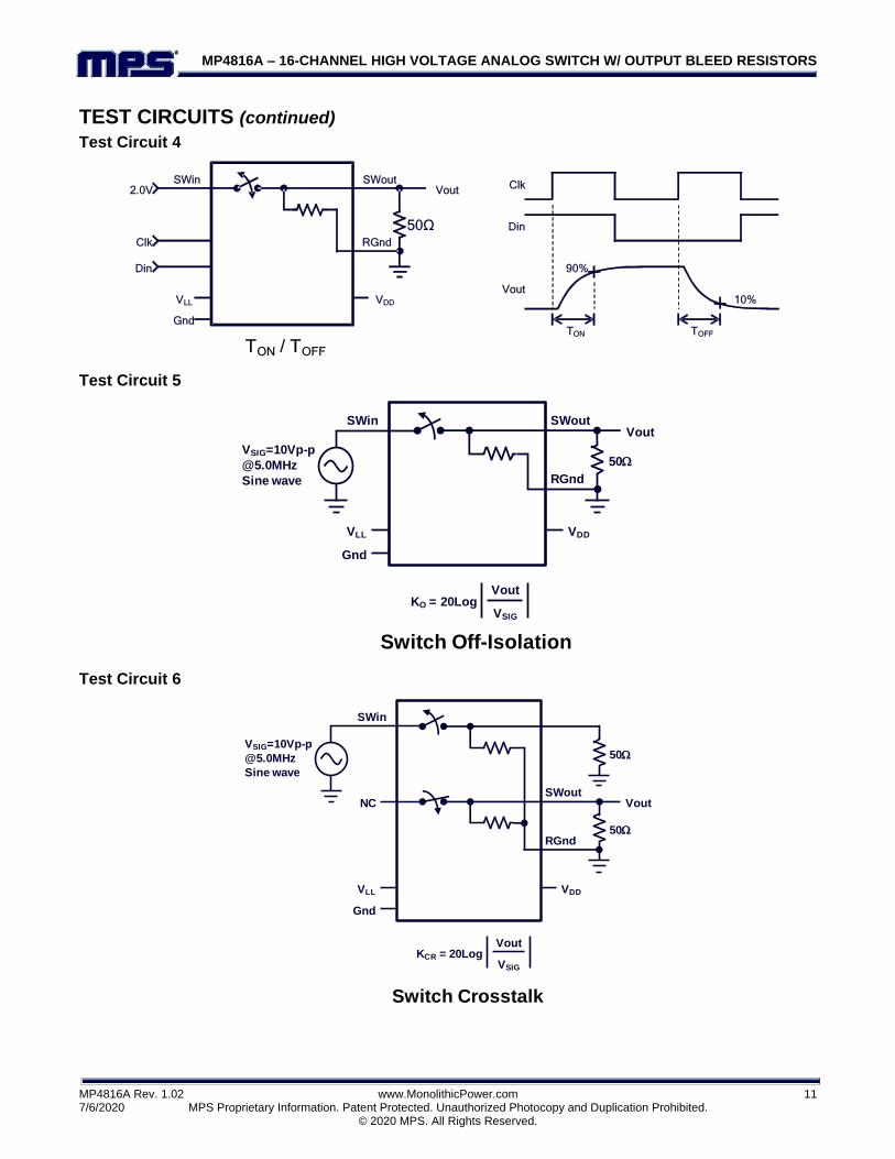
TEST CIRCUITS (continued) Test Circuit 7
VLL
Gnd
VDD
SWout
50W
Output Voltage Spike
1kW
SWin +VSPK
-VSPK
0V
Vout
RGnd
Test Circuit 8
Charge Injection
VLL
Gnd
VDD
SWoutSWinVout
1000pF
DVout
QINJ = 1000pF x DVout
RGnd
Test Circuit 9
VLL
VSIG=1.0Vp-p
Sine wave
Gnd
VDD
Vout
50W
Small Signal Bandwidth
SWoutSWin
RGnd

MP4816A – 16-CHANNEL HIGH VOLTAGE ANALOG SWITCH W/ OUTPUT BLEED RESISTORS
MP4816A Rev. 1.02 www.MonolithicPower.com 13 7/6/2020 MPS Proprietary Information. Patent Protected. Unauthorized Photocopy and Duplication Prohibited. © 2020 MPS. All Rights Reserved.
BLOCK DIAGRAM
Output
Switches
Level
ShiftersLatches
ClrLE\ VDD
Clk
Gnd
VLL
DIN
DOUT SWin-14
SWout-14
D
LE\
Clr
SWin-0
SWout-0
SWin-1
SWout-1
D
LE\
Clr
SWin-15
SWout-15
D
LE\
Clr
RGnd
D
LE\
Clr
16-Bit
ShiftRegister
Figure 1: Functional Block Diagram

MP4816A – 16-CHANNEL HIGH VOLTAGE ANALOG SWITCH W/ OUTPUT BLEED RESISTORS
MP4816A Rev. 1.02 www.MonolithicPower.com 14 7/6/2020 MPS Proprietary Information. Patent Protected. Unauthorized Photocopy and Duplication Prohibited. © 2020 MPS. All Rights Reserved.
APPLICATION INFORMATION The MP4816A is a 16-channel high-voltage, single-pole, single-throw, SPST, analog switch with integrated output bleed resistors designed for medical ultrasound imaging and non-destructive testing (NDT) applications. The MP4816A is designed to multiplex high transmit voltages to selected piezoelectric transducers and multiplex small analog echo signals to selected receivers.
The output switches are controlled by a 16-bit serial shift register followed by a 16-bit data latch. A data out pin (DOUT) allows for multiple devices to be cascaded together. This helps minimize the number of input/output (I/O) control lines. A logic high in the data latch turns on the corresponding analog switch. A logic low turns off the corresponding analog switch.
The MP4816A has a unique, patented design that does not require any high-voltage negative or positive supplies. This eliminates:
the need to generate high-voltage positive and negative supplies.
the need for high-voltage bypass capacitors next to each device.
safety concerns on high-voltage buses.
power-up/-down fault conditions concerns.
Analog Switch
The analog switches have a typical switch resistance of 12.5Ω. In the on state, the device can pass transmit voltages up to ±90V with peak currents of up to ±2.0A. In the off state, the device can block voltages up to ±90V.
Each switch has a dedicated input and output pin (SWin and SWout). The transmit voltages must be connected to the SWin pins. The PZT load must be connected to the SWout pins. The SWin and SWout pins are not interchangeable.
Typical high-voltage transmission waves are short bursts of high-voltage pulses. The burst can consists of single or multiple cycles of 1 - 15MHz pulses starting and ending at 0V (see Figure 2).
Figure 2: Typical Tx High Voltage Burst
The SWin input must be close to ground before sending the high-voltage pulses. This allows the internal circuitry to drive the output switches properly.
Transmit voltages greater than ±5V must have frequencies higher than 500kHz. When receiving the echo signals where the voltages are less than ±0.5V, there is no restriction. The switch can pass low-voltage DC signals.
Logic Interface
The MP4816A is controlled by a 16-bit serial shift register followed by a 16-bit latch. Data is loaded into the shift register during the rising edge of the clock. No data is transferred during the falling edge. Data is shifted into register 0 and is shifted out from register 15.
Register
0
Latch
0
Clk
DIN DOUT
LE\
Clr
SW0
Control
Register
14
Latch
14
SW14
Control
Register
15
Latch
15
SW15
Control
Figure 3: Logic Interface Details
Figure 3 shows the logic interface details. In the first clock cycle, the first data bit enters into shift register 0. After 15 more clocked cycles, the first bit is in register 15.
When the latch enable bar (LE\) is low, the data in the shift registers are transferred into the 16-bit latch. When LE\ is high, the data in the latches are held. With LE\ high, new data can be shifted into the 16-bit serial shift register without affecting the data in the 16-bit latch. The output switch states follow the data in the 16-bit latch. The Clr pin clears the data in the 16-bit latch only. Clr will not affect the data in the 16-bit serial shift register.

MP4816A – 16-CHANNEL HIGH VOLTAGE ANALOG SWITCH W/ OUTPUT BLEED RESISTORS
MP4816A Rev. 1.02 www.MonolithicPower.com 15 7/6/2020 MPS Proprietary Information. Patent Protected. Unauthorized Photocopy and Duplication Prohibited. © 2020 MPS. All Rights Reserved.
APPLICATION INFORMATION
Clk
DIN DOUT
LE\
Clk
DIN
Clr
MP4816A
U1
DOUT
LE\
Clk
DIN
Clr
DOUT
LE\
Clk
DIN
ClrLE\
Clr
MP4816A
U2
MP4816A
U12
Figure 4: Daisy-Chaining 12 MP4816A Devices with a Single Data Input Line
The maximum clock frequency for the MP4816A is 80MHz. The front-end logic control is designed to minimize the number of I/O control lines. A system requiring 192 channels needs 192 ÷ 16 = 12 devices. Figure 4 shows 12 MP4816A devices in a single daisy-chain configuration.
With an 80MHz clock, all 192 channels can be updated in 2.4µs. Only four control lines are required: clock, data in, latch enable bar, and clear. For systems requiring a faster update, multiple data in lines can be used (see Figure 5).
Clk
DINA DOUT
LE\
Clk
DIN
Clr
DOUT
LE\
Clk
DIN
Clr
DOUT
LE\
Clk
DIN
ClrLE\
Clr
DOUT
LE\
Clk
DIN
Clr
DOUT
LE\
Clk
DIN
Clr
DOUT
LE\
Clk
DIN
Clr
DOUT
LE\
Clk
DIN
Clr
DOUT
LE\
Clk
DIN
Clr
DOUT
LE\
Clk
DIN
Clr
DOUT
LE\
Clk
DIN
Clr
DOUT
LE\
Clk
DIN
Clr
DOUT
LE\
Clk
DIN
Clr
DINB
DINC
MP4816A
U1
MP4816A
U2
MP4816A
U3
MP4816A
U4
MP4816A
U5
MP4816A
U6
MP4816A
U7
MP4816A
U8
MP4816A
U9
MP4816A
U10
MP4816A
U11
MP4816A
U12
Figure 5: Daisy-Chaining MP4816A Devices with Multiple Data Input Lines
Figure 5 is a 192-channel system incorporating three data input lines (DINA, DINB, DINC). Each data input line addresses four MP4816A devices
daisy-chained together. There are now six control lines. With an 80MHz clock, all 192 channels can be updated in 800ns.

MP4816A – 16-CHANNEL HIGH VOLTAGE ANALOG SWITCH W/ OUTPUT BLEED RESISTORS
MP4816A Rev. 1.02 www.MonolithicPower.com 16 7/6/2020 MPS Proprietary Information. Patent Protected. Unauthorized Photocopy and Duplication Prohibited. © 2020 MPS. All Rights Reserved.
SWin-0 PZT-0
SWin-1 PZT-64
SWin-2 PZT-128
SWin-189 PZT- 63
SWin-190 PZT-127
SWin-191 PZT-191
Tx
RxT/R
SW
Tx-0
Tx
RxT/R
SW
Tx-63
Ultrasound ProbeUltrasound Console
192 Coaxial Cables
Figure 6: MP4816A in the Console
Figure 6 shows where the MP4816A analog switches reside in an ultrasound system. A 1:3 multiplexing configuration is shown as an example. Multiplexing configurations can range from 1:2 to 1:8 or higher. The 1:8 or higher ratios can have slower image frame rates and/or lower-quality images, which are generally used in the lower-end, lower-cost ultrasound market. The MP4816A can be used in any ratio.
The main advantage of using the MP4816A is that it reduces the number of transmitter and receiver circuitries. As shown in Figure 6, without any analog switches, the ultrasound console requires 192 transmitters and receivers to drive an ultrasound probe with 192 PZT elements. With analog switches, only 64 transmitters and receivers are needed. This reduction saves board space, power, and cost, since the transmitter and receiver circuitry can be quite complex. These benefits are especially important for portable ultrasound systems where space, battery life, and weight are all premiums.

MP4816A – 16-CHANNEL HIGH VOLTAGE ANALOG SWITCH W/ OUTPUT BLEED RESISTORS
MP4816A Rev. 1.02 www.MonolithicPower.com 17 7/6/2020 MPS Proprietary Information. Patent Protected. Unauthorized Photocopy and Duplication Prohibited. © 2020 MPS. All Rights Reserved.
SWin-0 PZT-0
SWin-1 PZT-64
SWin-2 PZT-128
SWin-189 PZT- 63
SWin-190 PZT-127
SWin-191 PZT-191
Tx
RxT/R
SW
Tx-0
Tx
RxT/R
SW
Tx-63
Ultrasound ProbeUltrasound Console
64 Coaxial Cables
Figure 7: MP4816A inside the Ultrasound Probe Head
Figure 7 shows the advantages of putting analog switches inside the probe head, which may be referred to as an active probe. Generally, the probe head is severely space-limited and thermally limited. The housing is waterproof since it must be submersed in alcohol for sterilization. By employing analog switches inside the probe head, the number of coaxial cables can be reduced. Instead of 192 coaxial cables, only 64 coaxial cables are needed for the PZT plus 10 or fewer additional coaxial cables for the supply lines and logic interface.
The reduction of coaxial cables required significantly reduces cost for the probe head. The coaxial cable is by far the most expensive item. Aside from the material cost, the labor to connect the coaxial cables is also quite costly. An added user benefit is that the probe head becomes more maneuverable. The sonographer experiences less fatigue using an active probe. Since the MP4816A does not need any high-voltage supplies, safety concerns about running high-voltage DC lines on the coaxial cables are eliminated, and the minimal power dissipation design eliminates the concern of thermal constraints inside the probe head, and the higher clock speed helps reduce the number of data lines.

MP4816A – 16-CHANNEL HIGH VOLTAGE ANALOG SWITCH W/ OUTPUT BLEED RESISTORS
MP4816A Rev. 1.02 www.MonolithicPower.com 18 7/6/2020 MPS Proprietary Information. Patent Protected. Unauthorized Photocopy and Duplication Prohibited. © 2020 MPS. All Rights Reserved.
PACKAGE INFORMATION
TQFP-48 (7mmx7mm)
PACKAGE OUTLINE DRAWING FOR 48L TQFP(7X7MM)
MF-PO-D-0243 revision 0.0
SIDE VIEW DETAIL "A"
NOTE:
1) ALL DIMENSIONS ARE IN MILLIMETERS.
2) PACKAGE LENGTH DOES NOT INCLUDE MOLD FLASH, PROTRUSION OR GATE BURR.
3) PACKAGE WITDH DOES NOT INCLUDE INTERLEAD FLASH OR PROTRUSION.
4) LEAD COPLANARITY (BOTTOM OF LEADS AFTER FORMING) SHALL BE 0.10 MILLIMETERS MAX.
5) JEDEC REFERENCE IS MO-143.
6) DRAWING IS NOT TO SCALE.
PIN 1 ID
TOP VIEW RECOMMENDED LAND PATTERN
SEE DETAIL "A"

MP4816A – 16-CHANNEL HIGH VOLTAGE ANALOG SWITCH W/ OUTPUT BLEED RESISTORS
NOTICE: The information in this document is subject to change without notice. Users should warrant and guarantee that third party Intellectual Property rights are not infringed upon when integrating MPS products into any application. MPS will not assume any legal responsibility for any said applications.
MP4816A Rev. 1.02 www.MonolithicPower.com 19 7/6/2020 MPS Proprietary Information. Patent Protected. Unauthorized Photocopy and Duplication Prohibited. © 2020 MPS. All Rights Reserved.
Revision History
Revision # Revision Date
Description Pages Updated
1.02 07/06/2020 Changing page 3, “1.0W to 1.47W Page 3