Embed Size (px)
Citation preview
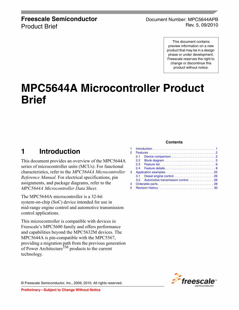
Freescale SemiconductorProduct Brief
Document Number: MPC5644APBRev. 5, 09/2010
Contents
© Freescale Semiconductor, Inc., 2009, 2010. All rights reserved.
Preliminary—Subject to Change Without Notice
This document contains preview information on a new
product that may be in a design phase or under development. Freescale reserves the right to
change or discontinue this product without notice.
1 Introduction This document provides an overview of the MPC5644A series of microcontroller units (MCUs). For functional characteristics, refer to the MPC5644A Microcontroller Reference Manual. For electrical specifications, pin assignments, and package diagrams, refer to the MPC5644A Microcontroller Data Sheet.
The MPC5644A microcontroller is a 32-bit system-on-chip (SoC) device intended for use in mid-range engine control and automotive transmission control applications.
This microcontroller is compatible with devices in Freescale’s MPC5600 family and offers performance and capabilities beyond the MPC5632M devices. The MPC5644A is pin-compatible with the MPC5567, providing a migration path from the previous generation of Power ArchitectureTM products to the current technology.
MPC5644A Microcontroller Product Brief
1 Introduction . . . . . . . . . . . . . . . . . . . . . . . . . . . . . . . . . . . . 12 Features . . . . . . . . . . . . . . . . . . . . . . . . . . . . . . . . . . . . . . 2
2.1 Device comparison . . . . . . . . . . . . . . . . . . . . . . . . . 22.2 Block diagram . . . . . . . . . . . . . . . . . . . . . . . . . . . . . 52.3 Feature list. . . . . . . . . . . . . . . . . . . . . . . . . . . . . . . . 62.4 Feature details. . . . . . . . . . . . . . . . . . . . . . . . . . . . . 8
3 Application examples . . . . . . . . . . . . . . . . . . . . . . . . . . . 253.1 Diesel engine control . . . . . . . . . . . . . . . . . . . . . . . 263.2 Automotive transmission control . . . . . . . . . . . . . . 26
4 Orderable parts . . . . . . . . . . . . . . . . . . . . . . . . . . . . . . . . 285 Revision history. . . . . . . . . . . . . . . . . . . . . . . . . . . . . . . . 30
MPC5644A Microcontroller Product Brief, Rev. 5
Preliminary—Subject to Change Without Notice
Features
Freescale Semiconductor2
The e200z4 host processor core of the MPC5644A complies with the Power ArchitectureTM Book E architecture and is 100% user mode compatible (with floating point library) with the classic PowerPC instruction set. In addition to the classic PowerPC instruction set, this core has additional instruction support for digital signal processing (DSP).
The MPC5644A has two levels of memory hierarchy consisting of 8 KB of instruction cache, backed by 192 KB on-chip SRAM and 4 MB of internal flash memory.
For development, the MPC5644A includes an external bus interface, and a calibration bus that is only accessible when using the Freescale Calibration System.
2 FeaturesThe following sections give an overview of MPC5644A features and compatibility.
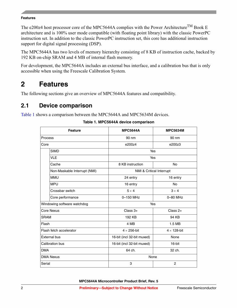
2.1 Device comparisonTable 1 shows a comparison between the MPC5644A and MPC5634M devices.
Table 1. MPC5644A device comparison
Feature MPC5644A MPC5634M
Process 90 nm 90 nm
Core e200z4 e200z3
SIMD Yes
VLE Yes
Cache 8 KB instruction No
Non-Maskable Interrupt (NMI) NMI & Critical Interrupt
MMU 24 entry 16 entry
MPU 16 entry No
Crossbar switch 5 4 3 4
Core performance 0–150 MHz 0–80 MHz
Windowing software watchdog Yes
Core Nexus Class 3+ Class 2+
SRAM 192 KB 94 KB
Flash 4 MB 1.5 MB
Flash fetch accelerator 4 256-bit 4 128-bit
External bus 16-bit (incl 32-bit muxed) None
Calibration bus 16-bit (incl 32-bit muxed) 16-bit
DMA 64 ch. 32 ch.
DMA Nexus None
Serial 3 2
Features
MPC5644A Microcontroller Product Brief, Rev. 5
Preliminary—Subject to Change Without NoticeFreescale Semiconductor 3
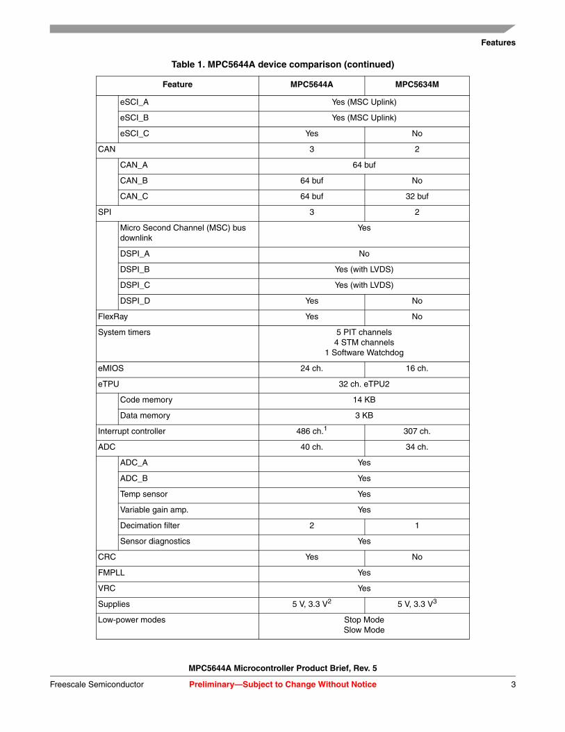
eSCI_A Yes (MSC Uplink)
eSCI_B Yes (MSC Uplink)
eSCI_C Yes No
CAN 3 2
CAN_A 64 buf
CAN_B 64 buf No
CAN_C 64 buf 32 buf
SPI 3 2
Micro Second Channel (MSC) bus downlink
Yes
DSPI_A No
DSPI_B Yes (with LVDS)
DSPI_C Yes (with LVDS)
DSPI_D Yes No
FlexRay Yes No
System timers 5 PIT channels4 STM channels
1 Software Watchdog
eMIOS 24 ch. 16 ch.
eTPU 32 ch. eTPU2
Code memory 14 KB
Data memory 3 KB
Interrupt controller 486 ch.1 307 ch.
ADC 40 ch. 34 ch.
ADC_A Yes
ADC_B Yes
Temp sensor Yes
Variable gain amp. Yes
Decimation filter 2 1
Sensor diagnostics Yes
CRC Yes No
FMPLL Yes
VRC Yes
Supplies 5 V, 3.3 V2 5 V, 3.3 V3
Low-power modes Stop ModeSlow Mode
Table 1. MPC5644A device comparison (continued)
Feature MPC5644A MPC5634M
MPC5644A Microcontroller Product Brief, Rev. 5
Preliminary—Subject to Change Without Notice
Features
Freescale Semiconductor4
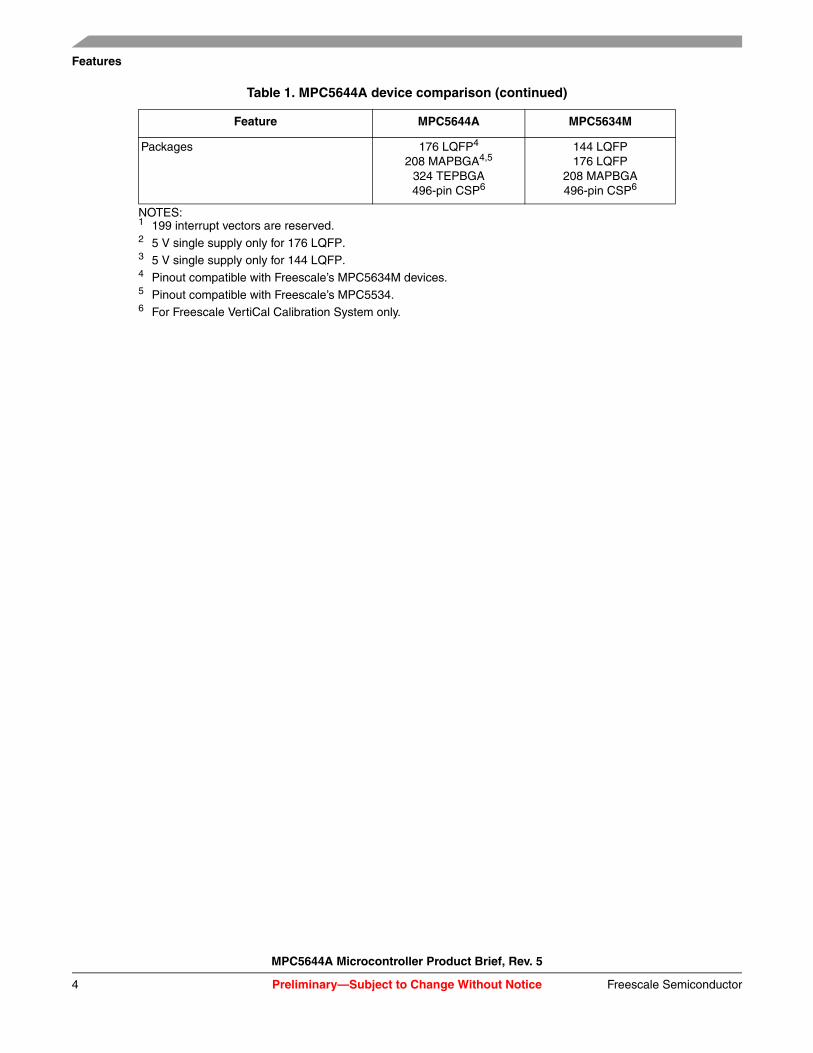
Packages 176 LQFP4
208 MAPBGA4,5
324 TEPBGA496-pin CSP6
144 LQFP176 LQFP
208 MAPBGA496-pin CSP6
NOTES:1 199 interrupt vectors are reserved.2 5 V single supply only for 176 LQFP.3 5 V single supply only for 144 LQFP.4 Pinout compatible with Freescale’s MPC5634M devices.5 Pinout compatible with Freescale’s MPC5534.6 For Freescale VertiCal Calibration System only.
Table 1. MPC5644A device comparison (continued)
Feature MPC5644A MPC5634M
Features
MPC5644A Microcontroller Product Brief, Rev. 5
Preliminary—Subject to Change Without NoticeFreescale Semiconductor 5
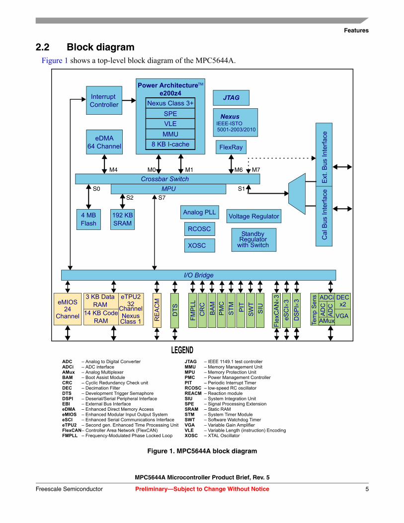
2.2 Block diagramFigure 1 shows a top-level block diagram of the MPC5644A.
Figure 1. MPC5644A block diagram
ADC – Analog to Digital ConverterADCi – ADC interfaceAMux – Analog MultiplexerBAM – Boot Assist ModuleCRC – Cyclic Redundancy Check unitDEC – Decimation FilterDTS – Development Trigger SemaphoreDSPI – Deserial/Serial Peripheral InterfaceEBI – External Bus InterfaceeDMA – Enhanced Direct Memory AccesseMIOS – Enhanced Modular Input Output SystemeSCI – Enhanced Serial Communications InterfaceeTPU2 – Second gen. Enhanced Time Processing UnitFlexCAN– Controller Area Network (FlexCAN)FMPLL – Frequency-Modulated Phase Locked Loop
JTAG – IEEE 1149.1 test controllerMMU – Memory Management UnitMPU – Memory Protection UnitPMC – Power Management ControllerPIT – Periodic Interrupt TimerRCOSC – low-speed RC oscillatorREACM – Reaction moduleSIU – System Integration UnitSPE – Signal Processing ExtensionSRAM – Static RAMSTM – System Timer ModuleSWT – Software Watchdog TimerVGA – Variable Gain AmplifierVLE – Variable Length (instruction) EncodingXOSC – XTAL Oscillator
LEGEND
eMIOS24
Channel
3 KB DataRAM
14 KB CodeRAM
eTPU232
ChannelTe
mp
Sen
s ADCi DECx2
VGAAD
CA
DC
AMux
4 MBFlash
192 KBSRAM
MPU
Crossbar Switch
InterruptController
eDMA64 Channel
SPE
VLE
MMU
8 KB I-cache
Power Architecturee200z4
TM
JTAG
NexusIEEE-ISTO5001-2003/2010
FlexRay
Ext
. B
us In
terf
ace
Cal
Bus
Inte
rfac
e
Fle
xCA
N3
Nexus Class 3+
Nexus
I/O Bridge
FM
PLL
CR
C
BA
M
PM
C
ST
M
PIT
SW
T
SIU
Analog PLL
RCOSC
XOSC
Voltage Regulator
StandbyRegulator
with Switch
DS
PI
3
eSC
I3
M4 M0 M6 M7
S0
S2 S7
S1
M1
RE
AC
M
DT
S
Class 1
MPC5644A Microcontroller Product Brief, Rev. 5
Preliminary—Subject to Change Without Notice
Features
Freescale Semiconductor6
2.3 Feature list• 150 MHz e200z4 Power Architecture core
— Variable length instruction encoding (VLE)
— Superscalar architecture with 2 execution units
— Up to 2 integer or floating point instructions per cycle
— Up to 4 multiply and accumulate operations per cycle
• Memory organization
— 4 MB on-chip flash memory with ECC and Read While Write (RWW)
— 192 KB on-chip RAM with standby functionality (32 KB) and ECC
— 8 KB instruction cache (with line locking), configurable as 2- or 4-way
— 14 + 3 KB eTPU code and data RAM
— 5 4 crossbar switch (XBAR)
— 24-entry MMU
— External Bus Interface (EBI) with slave and master port
• Fail Safe Protection
— 16-entry Memory Protection Unit (MPU)
— CRC unit with 3 sub-modules
— Junction temperature sensor
• Interrupts
— Configurable interrupt controller (with NMI)
— 64-channel DMA
• Serial channels
— 3 eSCI
— 3 DSPI (2 of which support downstream Micro Second Channel [MSC])
— 3 FlexCAN with 64 messages each
— 1 FlexRay module (V2.1) up to 10 Mbit/s with dual or single channel and 128 message objects and ECC
• 1 eMIOS
— 24 unified channels
• 1 eTPU2 (second generation eTPU)
— 32 standard channels
— 1 reaction module (6 channels with three outputs per channel)
• 2 enhanced queued analog-to-digital converters (eQADCs)
— Forty 12-bit input channels (multiplexed on 2 ADCs); expandable to 56 channels with external multiplexers
— 6 command queues
— Trigger and DMA support

Features
MPC5644A Microcontroller Product Brief, Rev. 5
Preliminary—Subject to Change Without NoticeFreescale Semiconductor 7
— 688 ns minimum conversion time
• On-chip CAN/SCI/FlexRay Bootstrap loader with Boot Assist Module (BAM)
• Nexus
— Class 3+ for the e200z4 core
— Class 1 for the eTPU
• JTAG (5-pin)
• Development Trigger Semaphore (DTS)
— Register of semaphores (32-bits) and an identification register
— Used as part of a triggered data acquisition protocol
— EVTO pin is used to communicate to the external tool
• Clock generation
— On-chip 4–40 MHz main oscillator
— On-chip FMPLL (frequency-modulated phase-locked loop)
• Up to 120 general purpose I/O lines
— Individually programmable as input, output or special function
— Programmable threshold (hysteresis)
• Power reduction mode: slow, stop and stand-by modes
• Flexible supply scheme
— 5 V single supply with external ballast
— Multiple external supply: 5 V, 3.3 V and 1.2 V
• Packages
— 176 LQFP
— 208 MAPBGA
— 324 TEPBGA
— 496-pin CSP (calibration tool only)
MPC5644A Microcontroller Product Brief, Rev. 5
Preliminary—Subject to Change Without Notice
Features
Freescale Semiconductor8
2.4 Feature details
2.4.1 e200z4d core
MPC5644A devices have a high performance e200z448n3 core processor:
• Dual issue, 32-bit Power Architecture embedded category CPU
• Variable Length Encoding Enhancements
• 8 KB instruction cache: 2- or 4- way set associative instruction cache
• Thirty-two 64-bit general purpose registers (GPRs)
• Memory management unit (MMU) with 24-entry fully-associative translation look-aside buffer (TLB)
• Harvard Architecture: Separate instruction bus and load/store bus
• Vectored interrupt support
• Non-maskable interrupt input
• Critical Interrupt input
• New ‘Wait for Interrupt’ instruction, to be used with new low power modes
• Reservation instructions for implementing read-modify-write accesses
• Signal processing extension (SPE) APU
• Single Precision Floating point (scalar and vector)
• Nexus Class 3+ debug
• Process ID manipulation for the MMU using an external tool
2.4.2 Crossbar Switch (XBAR)
The XBAR multiport crossbar switch supports simultaneous connections between five master ports and four slave ports. The crossbar supports a 32-bit address bus width and a 64-bit data bus width.
The crossbar allows three concurrent transactions to occur from the master ports to any slave port but each master must access a different slave. If a slave port is simultaneously requested by more than one master port, arbitration logic selects the higher priority master and grants it ownership of the slave port. All other masters requesting that slave port are stalled until the higher priority master completes its transactions. Requesting masters are treated with equal priority and are granted access to a slave port in round-robin fashion, based upon the ID of the last master to be granted access. The crossbar provides the following features:
• 5 master ports
— CPU instruction bus
— CPU data bus
— eDMA
— FlexRay
— External Bus Interface
• 4 slave ports
Features
MPC5644A Microcontroller Product Brief, Rev. 5
Preliminary—Subject to Change Without NoticeFreescale Semiconductor 9
— Flash
— Calibration and EBI bus
— SRAM
— Peripheral bridge
• 32-bit internal address, 64-bit internal data paths
2.4.3 eDMA
The enhanced direct memory access (eDMA) controller is a second-generation module capable of performing complex data movements via 64 programmable channels, with minimal intervention from the host processor. The hardware micro-architecture includes a DMA engine which performs source and destination address calculations, and the actual data movement operations, along with an SRAM-based memory containing the transfer control descriptors (TCD) for the channels. This implementation is utilized to minimize the overall block size. The eDMA module provides the following features:
• All data movement via dual-address transfers: read from source, write to destination
• Programmable source and destination addresses, transfer size, plus support for enhanced addressing modes
• Transfer control descriptor organized to support two-deep, nested transfer operations
• An inner data transfer loop defined by a “minor” byte transfer count
• An outer data transfer loop defined by a “major” iteration count
• Channel activation via one of three methods:
— Explicit software initiation
— Initiation via a channel-to-channel linking mechanism for continuous transfers
— Peripheral-paced hardware requests (one per channel)
• Support for fixed-priority and round-robin channel arbitration
• Channel completion reported via optional interrupt requests
• One interrupt per channel, optionally asserted at completion of major iteration count
• Error termination interrupts optionally enabled
• Support for scatter/gather DMA processing
• Ability to suspend channel transfers by a higher priority channel
2.4.4 Interrupt controller
The INTC (interrupt controller) provides priority-based preemptive scheduling of interrupt requests, suitable for statically scheduled hard real-time systems.
For high priority interrupt requests, the time from the assertion of the interrupt request from the peripheral to when the processor is executing the interrupt service routine (ISR) has been minimized. The INTC provides a unique vector for each interrupt request source for quick determination of which ISR needs to be executed. It also provides an ample number of priorities so that lower priority ISRs do not delay the execution of higher priority ISRs. To allow the appropriate priorities for each source of interrupt request, the priority of each interrupt request is software configurable.
MPC5644A Microcontroller Product Brief, Rev. 5
Preliminary—Subject to Change Without Notice
Features
Freescale Semiconductor10
When multiple tasks share a resource, coherent accesses to that resource need to be supported. The INTC supports the priority ceiling protocol for coherent accesses. By providing a modifiable priority mask, the priority can be raised temporarily so that all tasks which share the resource cannot preempt each other.
The INTC provides the following features:
• 9-bit vector addresses
• Unique vector for each interrupt request source
• Hardware connection to processor or read from register
• Each interrupt source can assigned a specific priority by software
• Preemptive prioritized interrupt requests to processor
• ISR at a higher priority preempts executing ISRs or tasks at lower priorities
• Automatic pushing or popping of preempted priority to or from a LIFO
• Ability to modify the ISR or task priority to implement the priority ceiling protocol for accessing shared resources
• Low latency—three clocks from receipt of interrupt request from peripheral to interrupt request to processor
This device also includes a non-maskable interrupt (NMI) pin that bypasses the INTC and multiplexing logic.
2.4.5 Memory protection unit (MPU)
The Memory Protection Unit (MPU) provides hardware access control for all memory references generated in a device. Using preprogrammed region descriptors, which define memory spaces and their associated access rights, the MPU concurrently monitors all system bus transactions and evaluates the appropriateness of each transfer. Memory references with sufficient access control rights are allowed to complete; references that are not mapped to any region descriptor or have insufficient rights are terminated with a protection error response.
The MPU has these major features:
• Support for 16 memory region descriptors, each 128 bits in size
— Specification of start and end addresses provide granularity for region sizes from 32 bytes to 4 GB
— MPU is invalid at reset, thus no access restrictions are enforced
— Two types of access control definitions: processor core bus master supports the traditional {read, write, execute} permissions with independent definitions for supervisor and user mode accesses; the remaining non-core bus masters (eDMA, FlexRay, and EBI1) support {read, write} attributes
— Automatic hardware maintenance of the region descriptor valid bit removes issues associated with maintaining a coherent image of the descriptor
— Alternate memory view of the access control word for each descriptor provides an efficient mechanism to dynamically alter the access rights of a descriptor only1
1. EBI not available on all packages and is not available, as a master, for customer.
Features
MPC5644A Microcontroller Product Brief, Rev. 5
Preliminary—Subject to Change Without NoticeFreescale Semiconductor 11
— For overlapping region descriptors, priority is given to permission granting over access denying as this approach provides more flexibility to system software
• Support for two XBAR slave port connections (SRAM and PBRIDGE)
— For each connected XBAR slave port (SRAM and PBRIDGE), MPU hardware monitors every port access using the pre-programmed memory region descriptors
— An access protection error is detected if a memory reference does not hit in any memory region or the reference is flagged as illegal in all memory regions where it does hit. In the event of an access error, the XBAR reference is terminated with an error response and the MPU inhibits the bus cycle being sent to the targeted slave device
— 64-bit error registers, one for each XBAR slave port, capture the last faulting address, attributes, and detail information
2.4.6 FMPLL
The FMPLL allows the user to generate high speed system clocks from a 4 MHz to 40 MHz crystal oscillator or external clock generator. Further, the FMPLL supports programmable frequency modulation of the system clock. The PLL multiplication factor, output clock divider ratio are all software configurable. The PLL has the following major features:
• Input clock frequency from 4 MHz to 40 MHz
• Reduced frequency divider (RFD) for reduced frequency operation without forcing the PLL to relock
• 3 modes of operation
— Bypass mode with PLL off
— Bypass mode with PLL running (default mode out of reset)
— PLL normal mode
• Each of the three modes may be run with a crystal oscillator or an external clock reference
• Programmable frequency modulation
— Modulation enabled/disabled through software
— Triangle wave modulation up to 100 kHz modulation frequency
— Programmable modulation depth (0% to 2% modulation depth)
— Programmable modulation frequency dependent on reference frequency
• Lock detect circuitry reports when the PLL has achieved frequency lock and continuously monitors lock status to report loss of lock conditions
• Clock Quality Module
— Detects the quality of the crystal clock and causes interrupt request or system reset if error is detected
— Detects the quality of the PLL output clock; if error detected, causes system reset or switches system clock to crystal clock and causes interrupt request
• Programmable interrupt request or system reset on loss of lock
• Self-clocked mode (SCM) operation
MPC5644A Microcontroller Product Brief, Rev. 5
Preliminary—Subject to Change Without Notice
Features
Freescale Semiconductor12
2.4.7 SIU
The MPC5644A SIU controls MCU reset configuration, pad configuration, external interrupt, general purpose I/O (GPIO), internal peripheral multiplexing, and the system reset operation. The reset configuration block contains the external pin boot configuration logic. The pad configuration block controls the static electrical characteristics of I/O pins. The GPIO block provides uniform and discrete input/output control of the I/O pins of the MCU. The reset controller performs reset monitoring of internal and external reset sources, and drives the RSTOUT pin. Communication between the SIU and the e200z4 CPU core is via the crossbar switch. The SIU provides the following features:
• System configuration
— MCU reset configuration via external pins
— Pad configuration control for each pad
— Pad configuration control for virtual I/O via DSPI serialization
• System reset monitoring and generation
— Power-on reset support
— Reset status register provides last reset source to software
— Glitch detection on reset input
— Software controlled reset assertion
• External interrupt
— Rising or falling edge event detection
— Programmable digital filter for glitch rejection
— Critical Interrupt request
— Non-Maskable Interrupt request
• GPIO
— Centralized control of I/O and bus pins
— Virtual GPIO via DSPI serialization (requires external deserialization device)
— Dedicated input and output registers for setting each GPIO and Virtual GPIO pin
• Internal multiplexing
— Allows serial and parallel chaining of DSPIs
— Allows flexible selection of eQADC trigger inputs
— Allows selection of interrupt requests between external pins and DSPI
2.4.8 Flash memory
The MPC5644A provides up to 4 MB of programmable, non-volatile, flash memory. The non-volatile memory (NVM) can be used to store instructions or data, or both. The flash module includes a Fetch Accelerator that optimizes the performance of the flash array to match the CPU architecture. The flash module interfaces the system bus to a dedicated flash memory array controller. For CPU ‘loads’, DMA transfers and CPU instruction fetch, it supports a 64-bit data bus width at the system bus port, and 128- and 256-bit read data interfaces to flash memory. The module contains a prefetch controller which
Features
MPC5644A Microcontroller Product Brief, Rev. 5
Preliminary—Subject to Change Without NoticeFreescale Semiconductor 13
prefetches sequential lines of data from the flash array into the buffers. Prefetch buffer hits allow no-wait responses.
The flash memory provides the following features:
• Supports a 64-bit data bus for instruction fetch, CPU loads and DMA access. Byte, halfword, word and doubleword reads are supported. Only aligned word and doubleword writes are supported.
• Fetch Accelerator
— Architected to optimize the performance of the flash
— Configurable read buffering and line prefetch support
— Four-entry 256-bit wide line read buffer
— Prefetch controller
• Hardware and software configurable read and write access protections on a per-master basis
• Interface to the flash array controller pipelined with a depth of one, allowing overlapped accesses to proceed in parallel for interleaved or pipelined flash array designs
• Configurable access timing usable in a wide range of system frequencies
• Multiple-mapping support and mapping-based block access timing (0-31 additional cycles) usable for emulation of other memory types
• Software programmable block program/erase restriction control
• Erase of selected block(s)
• Read page size of 128 bits (four words)
• ECC with single-bit correction, double-bit detection
• Program page size of 128 bits (four words) to accelerate programming
• ECC single-bit error corrections are visible to software
• Minimum program size is two consecutive 32-bit words, aligned on a 0-modulo-8 byte address, due to ECC
• Embedded hardware program and erase algorithm
• Erase suspend, program suspend and erase-suspended program
• Shadow information stored in non-volatile shadow block
• Independent program/erase of the shadow block
2.4.9 BAM
The BAM (Boot Assist Module) is a block of read-only memory that is programmed once by Freescale and is identical for all MPC5644A MCUs. The BAM program is executed every time the MCU is powered-on or reset in normal mode. The BAM supports different modes of booting. They are:
• Booting from internal flash memory
• Serial boot loading (A program is downloaded into RAM via eSCI or the FlexCAN and then executed)
• Booting from external memory on external bus
MPC5644A Microcontroller Product Brief, Rev. 5
Preliminary—Subject to Change Without Notice
Features
Freescale Semiconductor14
The BAM also reads the reset configuration half word (RCHW) from internal flash memory and configures the MPC5644A hardware accordingly. The BAM provides the following features:
• Sets up MMU to cover all resources and mapping of all physical addresses to logical addresses with minimum address translation
• Sets up MMU to allow user boot code to execute as either Power Architecture embedded category (default) or as Freescale VLE code
• Location and detection of user boot code
• Automatic switch to serial boot mode if internal flash is blank or invalid
• Supports user programmable 64-bit password protection for serial boot mode
• Supports serial bootloading via FlexCAN bus and eSCI using Freescale protocol
• Supports serial bootloading via FlexCAN bus and eSCI with auto baud rate sensing
• Supports serial bootloading of either Classic Power Architecture Book E code (default) or Freescale VLE code
• Supports booting from calibration bus interface
• Supports censorship protection for internal flash memory
• Provides an option to enable the core watchdog timer
• Provides an option to disable the system watchdog timer
2.4.10 eMIOS
The eMIOS timer module provides the capability to generate or measure events in hardware.
The eMIOS module features include:
• Twenty-four 24-bit wide channels
• 3 channels’ internal timebases can be shared between channels
• 1 Timebase from eTPU2 can be imported and used by the channels
• Global enable feature for all eMIOS and eTPU timebases
• Dedicated pin for each channel (not available on all package types)
Each channel (0–23) supports the following functions:
• General-purpose input/output (GPIO)
• Single-action input capture (SAIC)
• Single-action output compare (SAOC)
• Output pulse-width modulation buffered (OPWMB)
• Input period measurement (IPM)
• Input pulse-width measurement (IPWM)
• Double-action output compare (DAOC)
• Modulus counter buffered (MCB)
• Output pulse width and frequency modulation buffered (OPWFMB)
Features
MPC5644A Microcontroller Product Brief, Rev. 5
Preliminary—Subject to Change Without NoticeFreescale Semiconductor 15
2.4.11 eTPU2
The eTPU2 is an enhanced co-processor designed for timing control. Operating in parallel with the host CPU, the eTPU2 processes instructions and real-time input events, performs output waveform generation, and accesses shared data without host intervention. Consequently, for each timer event, the host CPU setup and service times are minimized or eliminated. A powerful timer subsystem is formed by combining the eTPU2 with its own instruction and data RAM. High-level assembler/compiler and documentation allows customers to develop their own functions on the eTPU2.
MPC5644A devices feature the second generation of the eTPU, called eTPU2. Enhancements of the eTPU2 over the standard eTPU include:
• The Timer Counter (TCR1), channel logic and digital filters (both channel and the external timer clock input [TCRCLK]) now have an option to run at full system clock speed or system clock / 2.
• Channels support unordered transitions: transition 2 can now be detected before transition 1. Related to this enhancement, the transition detection latches (TDL1 and TDL2) can now be independently negated by microcode.
• A new User Programmable Channel Mode has been added: the blocking, enabling, service request and capture characteristics of this channel mode can be programmed via microcode.
• Microinstructions now provide an option to issue Interrupt and Data Transfer requests selected by channel. They can also be requested simultaneously at the same instruction.
• Channel Flags 0 and 1 can now be tested for branching, in addition to selecting the entry point.
• Channel digital filters can be bypassed.
The eTPU2 includes these distinctive features:
• 32 channels; each channel associated with one input and one output signal
— Enhanced input digital filters on the input pins for improved noise immunity
— Identical, orthogonal channels: each channel can perform any time function. Each time function can be assigned to more than one channel at a given time, so each signal can have any functionality.
— Each channel has an event mechanism which supports single and double action functionality in various combinations. It includes two 24-bit capture registers, two 24-bit match registers, 24-bit greater-equal and equal-only comparators.
— Input and output signal states visible from the host
• 2 independent 24-bit time bases for channel synchronization:
— First time base clocked by system clock with programmable prescale division from 2 to 512 (in steps of 2), or by output of second time base prescaler
— Second time base counter can work as a continuous angle counter, enabling angle based applications to match angle instead of time
— Both time bases can be exported to the eMIOS timer module
— Both time bases visible from the host
• Event-triggered microengine:
— Fixed-length instruction execution in two-system-clock microcycle

MPC5644A Microcontroller Product Brief, Rev. 5
Preliminary—Subject to Change Without Notice
Features
Freescale Semiconductor16
— 14 KB of code memory (SCM)
— 3 KB of parameter (data) RAM (SPRAM)
— Parallel execution of data memory, ALU, channel control and flow control sub-instructions in selected combinations
— 32-bit microengine registers and 24-bit wide ALU, with 1 microcycle addition and subtraction, absolute value, bitwise logical operations on 24-bit, 16-bit, or byte operands, single-bit manipulation, shift operations, sign extension and conditional execution
— Additional 24-bit Multiply/MAC/Divide unit which supports all signed/unsigned Multiply/MAC combinations, and unsigned 24-bit divide. The MAC/Divide unit works in parallel with the regular microcode commands.
• Resource sharing features support channel use of common channel registers, memory and microengine time:
— Hardware scheduler works as a “task management” unit, dispatching event service routines by predefined, host-configured priority
— Automatic channel context switch when a “task switch” occurs, that is, one function thread ends and another begins to service a request from other channel: channel-specific registers, flags and parameter base address are automatically loaded for the next serviced channel
— SPRAM shared between host CPU and eTPU2, supporting communication either between channels and host or inter-channel
— Hardware implementation of four semaphores support coherent parameter sharing between both eTPU engines
— Dual-parameter coherency hardware support allows atomic access to two parameters by host
• Test and development support features:
— Nexus Class 1 debug, supporting single-step execution, arbitrary microinstruction execution, hardware breakpoints and watchpoints on several conditions
— Software breakpoints
— SCM continuous signature-check built-in self test (MISC - multiple input signature calculator), runs concurrently with eTPU2 normal operation
2.4.12 Reaction module
The reaction module provides the ability to modulate output signals to manage closed loop control without CPU assistance. It works in conjunction with the eQADC and eTPU2 to increase system performance by removing the CPU from the current control loop.
The reaction module has the following features:
• 6 reaction channels
• Each channel output is a bus of 3 signals, providing ability to control 3 inputs.
• Each channel can implement a peak and hold waveform, making it possible to implement up to six independent peak and hold control channels
Features
MPC5644A Microcontroller Product Brief, Rev. 5
Preliminary—Subject to Change Without NoticeFreescale Semiconductor 17
Target applications include solenoid control for direct injection systems and valve control in automatic transmissions
2.4.13 eQADC
The enhanced queued analog to digital converter (eQADC) block provides accurate and fast conversions for a wide range of applications. The eQADC provides a parallel interface to two on-chip analog to digital converters (ADC), and a single master to single slave serial interface to an off-chip external device. Both on-chip ADCs have access to all the analog channels.
The eQADC prioritizes and transfers commands from six command conversion command ‘queues’ to the on-chip ADCs or to the external device. The block can also receive data from the on-chip ADCs or from an off-chip external device into the six result queues, in parallel, independently of the command queues. The six command queues are prioritized with Queue_0 having the highest priority and Queue_5 the lowest. Queue_0 also has the added ability to bypass all buffering and queuing and abort a currently running conversion on either ADC and start a Queue_0 conversion. This means that Queue_0 will always have a deterministic time from trigger to start of conversion, irrespective of what tasks the ADCs were performing when the trigger occurred. The eQADC supports software and external hardware triggers from other blocks to initiate transfers of commands from the queues to the on-chip ADCs or to the external device. It also monitors the fullness of command queues and result queues, and accordingly generates DMA or interrupt requests to control data movement between the queues and the system memory, which is external to the eQADC.
The ADCs also support features designed to allow the direct connection of high impedance acoustic sensors that might be used in a system for detecting engine knock. These features include differential inputs; integrated variable gain amplifiers for increasing the dynamic range; programmable pull-up and pull-down resistors for biasing and sensor diagnostics.
The eQADC also integrates a programmable decimation filter capable of taking in ADC conversion results at a high rate, passing them through a hardware low pass filter, then down-sampling the output of the filter and feeding the lower sample rate results to the result FIFOs. This allows the ADCs to sample the sensor at a rate high enough to avoid aliasing of out-of-band noise; while providing a reduced sample rate output to minimize the amount DSP processing bandwidth required to fully process the digitized waveform.
The eQADC provides the following features:
• Dual on-chip ADCs
— 2 12-bit ADC resolution
— Programmable resolution for increased conversion speed (12-bit, 10-bit, 8-bit)
– 12-bit conversion time: 938 ns (1M sample/sec)
– 10-bit conversion time: 813 ns (1.2M sample/second)
– 8-bit conversion time: 688 ns (1.4M sample/second)
— Up to 10-bit accuracy at 500 KSample/s and 8-bit accuracy at 1 MSample/s
— Differential conversions
— Single-ended signal range from 0 to 5 V
— Variable gain amplifiers on differential inputs (1, 2, 4)
MPC5644A Microcontroller Product Brief, Rev. 5
Preliminary—Subject to Change Without Notice
Features
Freescale Semiconductor18
— Sample times of 2 (default), 8, 64 or 128 ADC clock cycles
— Provides time stamp information when requested
— Allows time stamp information relative to eTPU clock sources, such as an angle clock
— Parallel interface to eQADC CFIFOs and RFIFOs
— Supports both right-justified unsigned and signed formats for conversion results
• 40 single-ended input channels, expandable to 56 channels with external multiplexers (supports four external 8-to-1 muxes)
• 8 channels can be used as 4 pairs of differential analog input channels
• Differential channels include variable gain amplifier for improved dynamic range
• Differential channels include programmable pull-up and pull-down resistors for biasing and sensor diagnostics (200 k100 k5 k
• Additional internal channels for monitoring voltages (such as core voltage, I/O voltage, LVI voltages, etc.) inside the device
• An internal bandgap reference to allow absolute voltage measurements
• 4 pairs of differential analog input channels
— Programmable pull-up/pull-down resistors on each differential input for biasing and sensor diagnostic (200 k, 100 k, 5 k)
• Silicon die temperature sensor
— Provides temperature of silicon as an analog value
— Read using an internal ADC analog channel
— May be read with either ADC
• 2 Decimation Filters
— Programmable decimation factor (1 to 16)
— Selectable IIR or FIR filter
— Up to 4th order IIR or 8th order FIR
— Programmable coefficients
— Saturated or non-saturated modes
— Programmable Rounding (Convergent; Two’s Complement; Truncated)
— Prefill mode to precondition the filter before the sample window opens
— Supports Multiple Cascading Decimation Filters to implement more complex filter designs
— Optional Absolute Integrators on the output of Decimation Filters
• Full duplex synchronous serial interface to an external device
— Free-running clock for use by an external device
— Supports a 26-bit message length
• Priority based Queues
— Supports six Queues with fixed priority. When commands of distinct Queues are bound for the same ADC, the higher priority Queue is always served first
Features
MPC5644A Microcontroller Product Brief, Rev. 5
Preliminary—Subject to Change Without NoticeFreescale Semiconductor 19
— Queue_0 can bypass all prioritization, buffering and abort current conversions to start a Queue_0 conversion a deterministic time after the queue trigger
— Supports software and hardware trigger modes to arm a particular Queue
— Generates interrupt when command coherency is not achieved
• External hardware triggers
— Supports rising edge, falling edge, high level and low level triggers
— Supports configurable digital filter
2.4.14 DSPI
The deserial serial peripheral interface (DSPI) block provides a synchronous serial interface for communication between the MPC5644A MCU and external devices. The DSPI supports pin count reduction through serialization and deserialization of eTPU and eMIOS channels and memory-mapped registers. The channels and register content are transmitted using a SPI-like protocol. This SPI-like protocol is completely configurable for baud rate, polarity and phase, frame length, chip select assertion, etc. Each bit in the frame may be configured to serialize either eTPU channels, eMIOS channels or GPIO signals. The DSPI can be configured to serialize data to an external device that implements the Microsecond Bus protocol. There are three identical DSPI blocks on the MPC5644A MCU. The DSPI pins support 5 V logic levels or Low Voltage Differential Signalling (LVDS) to improve high speed operation.
DSPI module features include:
• Selectable LVDS pads working at 40 MHZ for SOUT and SCK pins for DSPI_B and DSPI_C
• 3 sources of serialized data: eTPU_A, eMIOS output channels and memory-mapped register in the DSPI
• 4 destinations for deserialized data: eTPU_A and eMIOS input channels, SIU external Interrupt input request, memory-mapped register in the DSPI
• 32-bit DSI and TSB modes require 32 PCR registers, 32 GPO and GPI registers in the SIU to select either GPIO, eTPU or eMIOS bits for serialization
• The DSPI Module can generate and check parity in a serial frame
2.4.15 eSCI
Three enhanced serial communications interface (eSCI) modules provide asynchronous serial communications with peripheral devices and other MCUs, and include support to interface to Local Interconnect Network (LIN) slave devices. Each eSCI block provides the following features:
• Full-duplex operation
• Standard mark/space non-return-to-zero (NRZ) format
• 13-bit baud rate selection
• Programmable 8-bit or 9-bit, data format
• Programmable 12-bit or 13-bit data format for Timed Serial Bus (TSB) configuration to support the Microsecond bus standard
• Automatic parity generation
MPC5644A Microcontroller Product Brief, Rev. 5
Preliminary—Subject to Change Without Notice
Features
Freescale Semiconductor20
• LIN support
— Autonomous transmission of entire frames
— Configurable to support all revisions of the LIN standard
— Automatic parity bit generation
— Double stop bit after bit error
— 10- or 13-bit break support
• Separately enabled transmitter and receiver
• Programmable transmitter output parity
• 2 receiver wake-up methods:
— Idle line wake-up
— Address mark wake-up
• Interrupt-driven operation with flags
• Receiver framing error detection
• Hardware parity checking
• 1/16 bit-time noise detection
• DMA support for both transmit and receive data
— Global error bit stored with receive data in system RAM to allow post processing of errors
2.4.16 FlexCAN
The MPC5644A MCU includes three controller area network (FlexCAN) blocks. The FlexCAN module is a communication controller implementing the CAN protocol according to Bosch Specification version 2.0B. The CAN protocol was designed to be used primarily as a vehicle serial data bus, meeting the specific requirements of this field: real-time processing, reliable operation in the EMI environment of a vehicle, cost-effectiveness and required bandwidth. Each FlexCAN module contains 64 message buffers.
The FlexCAN modules provide the following features:
• Based on and including all existing features of the Freescale TouCAN module
• Full Implementation of the CAN protocol specification, Version 2.0B
— Standard data and remote frames
— Extended data and remote frames
— Zero to eight bytes data length
— Programmable bit rate up to 1 Mbit/s
• Content-related addressing
• 64 message buffers of zero to eight bytes data length
• Individual Rx Mask Register per message buffer
• Each message buffer configurable as Rx or Tx, all supporting standard and extended messages
• Includes 1088 bytes of embedded memory for message buffer storage
• Includes 256-byte memory for storing individual Rx mask registers

Features
MPC5644A Microcontroller Product Brief, Rev. 5
Preliminary—Subject to Change Without NoticeFreescale Semiconductor 21
• Full featured Rx FIFO with storage capacity for six frames and internal pointer handling
• Powerful Rx FIFO ID filtering, capable of matching incoming IDs against 8 extended, 16 standard or 32 partial (8 bits) IDs, with individual masking capability
• Selectable backwards compatibility with previous FlexCAN versions
• Programmable clock source to the CAN Protocol Interface, either system clock or oscillator clock
• Listen only mode capability
• Programmable loop-back mode supporting self-test operation
• 3 programmable Mask Registers
• Programmable transmit-first scheme: lowest ID, lowest buffer number or highest priority
• Time Stamp based on 16-bit free-running timer
• Global network time, synchronized by a specific message
• Maskable interrupts
• Warning interrupts when the Rx and Tx Error Counters reach 96
• Independent of the transmission medium (an external transceiver is assumed)
• Multi-master concept
• High immunity to EMI
• Short latency time due to an arbitration scheme for high-priority messages
• Low power mode, with programmable wake-up on bus activity
2.4.17 FlexRay
The MPC5644A includes one dual-channel FlexRay module that implements the FlexRay Communications System Protocol Specification, Version 2.1 Rev A. Features include:
• Single channel support
• FlexRay bus data rates of 10 Mbit/s, 8 Mbit/s, 5 Mbit/s, and 2.5 Mbit/s supported
• 128 message buffers, each configurable as:
— Receive message buffer
— Single buffered transmit message buffer
— Double buffered transmit message buffer (combines two single buffered message buffer)
• 2 independent receive FIFOs
— 1 receive FIFO per channel
— Up to 255 entries for each FIFO
• ECC support
2.4.18 System timers
The system timers include two distinct types of system timer:
• Periodic interrupts/triggers using the Periodic Interrupt Timer (PIT)
• Operating system task monitors using the System Timer Module (STM)
MPC5644A Microcontroller Product Brief, Rev. 5
Preliminary—Subject to Change Without Notice
Features
Freescale Semiconductor22
2.4.18.1 Periodic interrupt timer (PIT)
The PIT provides five independent timer channels, capable of producing periodic interrupts and periodic triggers. The PIT has no external input or output pins and is intended to provide system ‘tick’ signals to the operating system, as well as periodic triggers for eQADC queues. Of the five channels in the PIT, four are clocked by the system clock and one is clocked by the crystal clock. This one channel is also referred to as Real-Time Interrupt (RTI) and is used to wake up the device from low power stop mode.
The following features are implemented in the PIT:
• 5 independent timer channels
• Each channel includes 32-bit wide down counter with automatic reload
• 4 channels clocked from system clock
• 1 channel clocked from crystal clock (wake-up timer)
• Wake-up timer remains active when System STOP mode is entered; used to restart system clock after predefined time-out period
• Each channel optionally able to generate an interrupt request or a trigger event (to trigger eQADC queues) when timer reaches zero
2.4.18.2 System timer module (STM)
The System Timer Module (STM) is designed to implement the software task monitor as defined by AUTOSAR1. It consists of a single 32-bit counter, clocked by the system clock, and four independent timer comparators. These comparators produce a CPU interrupt when the timer exceeds the programmed value.
The following features are implemented in the STM:
• One 32-bit up counter with 8-bit prescaler
• Four 32-bit compare channels
• Independent interrupt source for each channel
• Counter can be stopped in debug mode
2.4.19 Software watchdog timer (SWT)
The Software Watchdog Timer (SWT) is a second watchdog module to complement the standard Power Architecture watchdog integrated in the CPU core. The SWT is a 32-bit modulus counter, clocked by the system clock or the crystal clock, that can provide a system reset or interrupt request when the correct software key is not written within the required time window.
The following features are implemented:
• 32-bit modulus counter
• Clocked by system clock or crystal clock
• Optional programmable watchdog window mode
• Can optionally cause system reset or interrupt request on timeout
1.AUTOSAR: AUTomotive Open System ARchitecture (see http://www.autosar.org)
Features
MPC5644A Microcontroller Product Brief, Rev. 5
Preliminary—Subject to Change Without NoticeFreescale Semiconductor 23
• Reset by writing a software key to memory mapped register
• Enabled out of reset
• Configuration is protected by a software key or a write-once register
2.4.20 Cyclic redundancy check (CRC) module
The CRC computing unit is dedicated to the computation of CRC off-loading the CPU. The CRC features:
• Support for CRC-16-CCITT (x25 protocol):
— X16 + X12 + X5 + 1
• Support for CRC-32 (Ethernet protocol):
— X32 + X26 + X23 + X22 + X16 + X12 + X11 + X10 + X8 + X7 + X5 + X4 + X2 + X + 1
• Zero wait states for each write/read operations to the CRC_CFG and CRC_INP registers at the maximum frequency
2.4.21 Error correction status module (ECSM)
The ECSM provides a myriad of miscellaneous control functions regarding program-visible information about the platform configuration and revision levels, a reset status register, a software watchdog timer, wakeup control for exiting sleep modes, and information on platform memory errors reported by error-correcting codes and/or generic access error information for certain processor cores.
The Error Correction Status Module supports a number of miscellaneous control functions for the platform. The ECSM includes these features:
• Registers for capturing information on platform memory errors if error-correcting codes (ECC) are implemented
• For test purposes, optional registers to specify the generation of double-bit memory errors are enabled on the MPC5644A.
The sources of the ECC errors are:
• Flash
• SRAM
• Peripheral RAM (FlexRay, CAN, eTPU2 Parameter RAM)
2.4.22 External bus interface (EBI)
The MPC5644A device features an external bus interface that is available in 324 TEPBGA and calibration packages.
The EBI supports operation at frequencies of system clock /1, /2 and /4, with a maximum frequency support of 80 MHz. Customers running the device at 120 MHz or 132 MHz will use the /2 divider, giving an EBI frequency of 60 MHz or 66 MHz. Customers running the device at 80 MHz will be able to use the /1 divider to have the EBI run at the full 80 MHz frequency.
Features include:
MPC5644A Microcontroller Product Brief, Rev. 5
Preliminary—Subject to Change Without Notice
Features
Freescale Semiconductor24
• 1.8 V to 3.3 V ± 10% I/O (1.6 V to 3.6 V)
• Memory controller with support for various memory types
• 16-bit data bus, up to 22-bit address bus
• Pin muxing included to support 32-bit muxed bus
• Selectable drive strength
• Configurable bus speed modes
• Bus monitor
• Configurable wait states
2.4.23 Calibration EBI
The Calibration EBI controls data transfer across the crossbar switch to/from memories or peripherals attached to the VertiCal connector in the calibration address space. The Calibration EBI is only available in the VertiCal Calibration System.
Features include:
• 1.8 V to 3.3 V ± 10% I/O (1.6 V to 3.6 V)
• Memory controller supports various memory types
• 16-bit data bus, up to 22-bit address bus
• Pin muxing supports 32-bit muxed bus
• Selectable drive strength
• Configurable bus speed modes
• Bus monitor
• Configurable wait states
2.4.24 Power management controller (PMC)
The power management controller contains circuitry to generate the internal 3.3 V supply and to control the regulation of 1.2 V supply with an external NPN ballast transistor. It also contains low voltage inhibit (LVI) and power-on reset (POR) circuits for the 1.2 V supply, the 3.3 V supply, the 3.3 V/5 V supply of the closest I/O segment (VDDEH1) and the 5 V supply of the regulators (VDDREG).
2.4.25 Nexus port controller
The NPC (Nexus Port Controller) block provides real-time Nexus Class3+ development support capabilities for the MPC5644A Power Architecture-based MCU in compliance with the IEEE-ISTO 5001-2003 and 2010 standards. MDO port widths of 4 pins and 12 pins are available in all packages.
2.4.26 JTAG
The JTAGC (JTAG Controller) block provides the means to test chip functionality and connectivity while remaining transparent to system logic when not in test mode. Testing is performed via a boundary scan technique, as defined in the IEEE 1149.1-2001 standard. All data input to and output from the JTAGC
Application examples
MPC5644A Microcontroller Product Brief, Rev. 5
Preliminary—Subject to Change Without NoticeFreescale Semiconductor 25
block is communicated in serial format. The JTAGC block is compliant with the IEEE 1149.1-2001 standard and supports the following features:
• IEEE 1149.1-2001 Test Access Port (TAP) interface 4 pins (TDI, TMS, TCK, and TDO)
• A 5-bit instruction register that supports the following IEEE 1149.1-2001 defined instructions:
— BYPASS, IDCODE, EXTEST, SAMPLE, SAMPLE/PRELOAD, HIGHZ, CLAMP
• A 5-bit instruction register that supports the additional following public instructions:
— ACCESS_AUX_TAP_NPC
— ACCESS_AUX_TAP_ONCE
— ACCESS_AUX_TAP_eTPU
— ACCESS_CENSOR
• 3 test data registers to support JTAG Boundary Scan mode
— Bypass register
— Boundary scan register
— Device identification register
• A TAP controller state machine that controls the operation of the data registers, instruction register and associated circuitry
• Censorship Inhibit Register
— 64-bit Censorship password register
— If the external tool writes a 64-bit password that matches the Serial Boot password stored in the internal flash shadow row, Censorship is disabled until the next system reset.
2.4.27 Development Trigger Semaphore (DTS)
MPC5644A devices include a system development feature, the Development Trigger Semaphore (DTS) module, that enables software to signal an external tool by driving a persistent (affected only by reset or an external tool) signal on an external device pin. There is a variety of ways this module can be used, including as a component of an external real-time data acquisition system
3 Application examplesThe MPC5644A is intended for use in two main categories of applications:
• Mid-range engine control
— 4-cylinder diesel engine control
— 4-cylinder gasoline engine control
• Automotive transmission control
— Electro-hydraulic automatic gearbox control
— Robotized automatic gearbox control
MPC5644A Microcontroller Product Brief, Rev. 5
Preliminary—Subject to Change Without Notice
Application examples
Freescale Semiconductor26
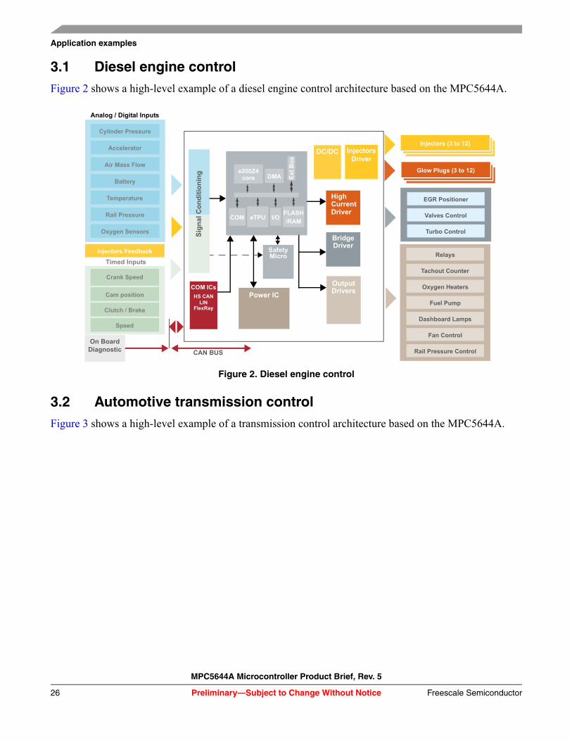
3.1 Diesel engine controlFigure 2 shows a high-level example of a diesel engine control architecture based on the MPC5644A.
Figure 2. Diesel engine control
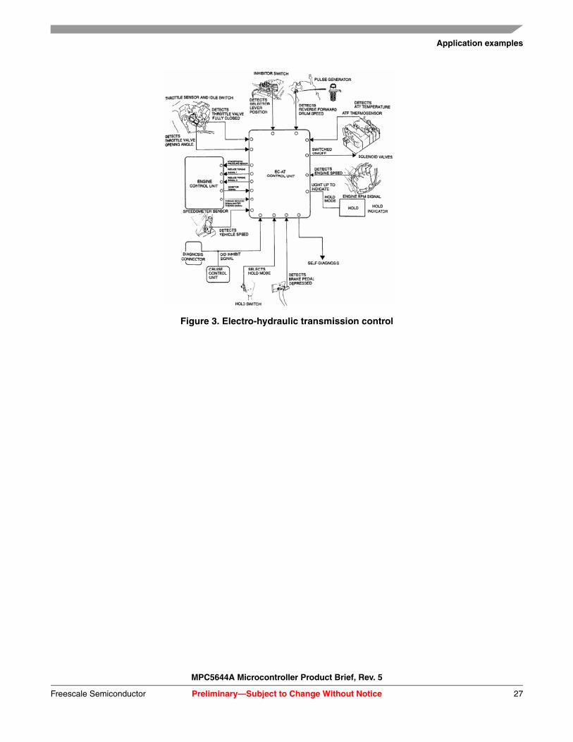
3.2 Automotive transmission controlFigure 3 shows a high-level example of a transmission control architecture based on the MPC5644A.
Relays
Tachout Counter
Oxygen Heaters
Fuel Pump
Dashboard Lamps
Rail Pressure Control
Fan Control
EGR Positioner
Valves Control
Turbo Control
Glow Plugs (3 to 12)
Injectors (3 to 12)
Crank Speed
Cam position
Clutch / Brake
Speed
Timed Inputs
Injectors Feedback
Cylinder Pressure
Accelerator
Air Mass Flow
Battery
Temperature
Rail Pressure
Oxygen Sensors Sig
nal
Co
nd
itio
nin
g
COM ICs
HS CANLIN
FlexRay
Power IC
SafetyMicro
OutputDrivers
BridgeDriver
High
DriverCurrent
DC/DC InjectorsDriver
COM eTPU I/OFLASH
/RAM
DMA Ext
Bu
s
e200Z4core
On BoardDiagnostic CAN BUS
Cylinder Pressure
Accelerator
Analog / Digital Inputs
Application examples
MPC5644A Microcontroller Product Brief, Rev. 5
Preliminary—Subject to Change Without NoticeFreescale Semiconductor 27
Figure 3. Electro-hydraulic transmission control
MPC5644A Microcontroller Product Brief, Rev. 5
Preliminary—Subject to Change Without Notice
Orderable parts
Freescale Semiconductor28
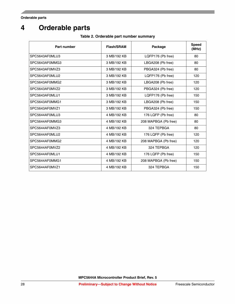
4 Orderable partsTable 2. Orderable part number summary
Part number Flash/SRAM PackageSpeed (MHz)
SPC5643AF0MLU3 3 MB/192 KB LQFP176 (Pb free) 80
SPC5643AF0MMG3 3 MB/192 KB LBGA208 (Pb free) 80
SPC5643AF0MVZ3 3 MB/192 KB PBGA324 (Pb free) 80
SPC5643AF0MLU2 3 MB/192 KB LQFP176 (Pb free) 120
SPC5643AF0MMG2 3 MB/192 KB LBGA208 (Pb free) 120
SPC5643AF0MVZ2 3 MB/192 KB PBGA324 (Pb free) 120
SPC5643AF0MLU1 3 MB/192 KB LQFP176 (Pb free) 150
SPC5643AF0MMG1 3 MB/192 KB LBGA208 (Pb free) 150
SPC5643AF0MVZ1 3 MB/192 KB PBGA324 (Pb free) 150
SPC5644AF0MLU3 4 MB/192 KB 176 LQFP (Pb free) 80
SPC5644AF0MMG3 4 MB/192 KB 208 MAPBGA (Pb free) 80
SPC5644AF0MVZ3 4 MB/192 KB 324 TEPBGA 80
SPC5644AF0MLU2 4 MB/192 KB 176 LQFP (Pb free) 120
SPC5644AF0MMG2 4 MB/192 KB 208 MAPBGA (Pb free) 120
SPC5644AF0MVZ2 4 MB/192 KB 324 TEPBGA 120
SPC5644AF0MLU1 4 MB/192 KB 176 LQFP (Pb free) 150
SPC5644AF0MMG1 4 MB/192 KB 208 MAPBGA (Pb free) 150
SPC5644AF0MVZ1 4 MB/192 KB 324 TEPBGA 150

Orderable parts
MPC5644A Microcontroller Product Brief, Rev. 5
Preliminary—Subject to Change Without NoticeFreescale Semiconductor 29
Figure 4. Commercial orderable part structure
Qualification Status
Product Family
ATMC Fab and Mask Revision
Temperature Range
Package
Maximum Frequency
SPC 5644A 1Example code: M VZ
Qualification StatusMPC = Industrial qualifiedSPC = Automotive qualifiedPC = Prototype
Product5644A= MPC5644A family
Fab and Mask RevisionF = ATMC0 = Revision
Temperature spec.M = –40°C to 125°C
Package CodeLU = 176 LQFPMG = 208 MAPBGAVZ = 324 TEPBGA
Maximum Frequency1 = 150 MHz2 = 120 MHz3 = 80 MHz
F0
MPC5644A Microcontroller Product Brief, Rev. 5
Preliminary—Subject to Change Without Notice
Revision history
Freescale Semiconductor30
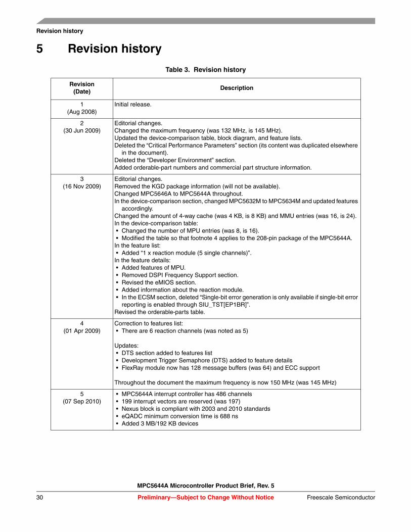
5 Revision history
Table 3. Revision history
Revision(Date)
Description
1(Aug 2008)
Initial release.
2(30 Jun 2009)
Editorial changes.Changed the maximum frequency (was 132 MHz, is 145 MHz).Updated the device-comparison table, block diagram, and feature lists.Deleted the “Critical Performance Parameters” section (its content was duplicated elsewhere
in the document).Deleted the “Developer Environment” section.Added orderable-part numbers and commercial part structure information.
3(16 Nov 2009)
Editorial changes.Removed the KGD package information (will not be available).Changed MPC5646A to MPC5644A throughout.In the device-comparison section, changed MPC5632M to MPC5634M and updated features
accordingly.Changed the amount of 4-way cache (was 4 KB, is 8 KB) and MMU entries (was 16, is 24).In the device-comparison table: • Changed the number of MPU entries (was 8, is 16). • Modified the table so that footnote 4 applies to the 208-pin package of the MPC5644A.In the feature list: • Added “1 x reaction module (5 single channels)”.In the feature details: • Added features of MPU. • Removed DSPI Frequency Support section. • Revised the eMIOS section. • Added information about the reaction module. • In the ECSM section, deleted “Single-bit error generation is only available if single-bit error
reporting is enabled through SIU_TST[EP1BR]”.Revised the orderable-parts table.
4(01 Apr 2009)
Correction to features list: • There are 6 reaction channels (was noted as 5)
Updates: • DTS section added to features list • Development Trigger Semaphore (DTS) added to feature details • FlexRay module now has 128 message buffers (was 64) and ECC support
Throughout the document the maximum frequency is now 150 MHz (was 145 MHz)
5(07 Sep 2010)
• MPC5644A interrupt controller has 486 channels • 199 interrupt vectors are reserved (was 197) • Nexus block is compliant with 2003 and 2010 standards • eQADC minimum conversion time is 688 ns • Added 3 MB/192 KB devices

MPC5644A Microcontroller Product Brief, Rev. 5
Preliminary—Subject to Change Without NoticeFreescale Semiconductor 31
THIS PAGE IS INTENTIONALLY BLANK

Document Number: MPC5644APBRev. 509/2010
How to Reach Us:
Home Page:www.freescale.com
Web Support:http://www.freescale.com/support
USA/Europe or Locations Not Listed:Freescale Semiconductor, Inc.Technical Information Center, EL5162100 East Elliot RoadTempe, Arizona 852841-800-521-6274 or +1-480-768-2130www.freescale.com/support
Europe, Middle East, and Africa:Freescale Halbleiter Deutschland GmbHTechnical Information CenterSchatzbogen 781829 Muenchen, Germany+44 1296 380 456 (English)+46 8 52200080 (English)+49 89 92103 559 (German)+33 1 69 35 48 48 (French)www.freescale.com/support
Japan:Freescale Semiconductor Japan Ltd.HeadquartersARCO Tower 15F1-8-1, Shimo-Meguro, Meguro-ku,Tokyo 153-0064Japan0120 191014 or +81 3 5437 [email protected]
Asia/Pacific:Freescale Semiconductor China Ltd.Exchange Building 23FNo. 118 Jianguo RoadChaoyang DistrictBeijing 100022 China +86 10 5879 [email protected]
For Literature Requests Only:Freescale Semiconductor Literature Distribution Center1-800-441-2447 or +1-303-675-2140Fax: [email protected]
Information in this document is provided solely to enable system and software implementers to use Freescale Semiconductor products. There are no express or implied copyright licenses granted hereunder to design or fabricate any integrated circuits or integrated circuits based on the information in this document.
Freescale Semiconductor reserves the right to make changes without further notice to any products herein. Freescale Semiconductor makes no warranty, representation or guarantee regarding the suitability of its products for any particular purpose, nor does Freescale Semiconductor assume any liability arising out of the application or use of any product or circuit, and specifically disclaims any and all liability, including without limitation consequential or incidental damages. “Typical” parameters that may be provided in Freescale Semiconductor data sheets and/or specifications can and do vary in different applications and actual performance may vary over time. All operating parameters, including “Typicals”, must be validated for each customer application by customer’s technical experts. Freescale Semiconductor does not convey any license under its patent rights nor the rights of others. Freescale Semiconductor products are not designed, intended, or authorized for use as components in systems intended for surgical implant into the body, or other applications intended to support or sustain life, or for any other application in which the failure of the Freescale Semiconductor product could create a situation where personal injury or death may occur. Should Buyer purchase or use Freescale Semiconductor products for any such unintended or unauthorized application, Buyer shall indemnify and hold Freescale Semiconductor and its officers, employees, subsidiaries, affiliates, and distributors harmless against all claims, costs, damages, and expenses, and reasonable attorney fees arising out of, directly or indirectly, any claim of personal injury or death associated with such unintended or unauthorized use, even if such claim alleges that Freescale Semiconductor was negligent regarding the design or manufacture of the part.
Freescale™ and the Freescale logo are trademarks of Freescale Semiconductor, Inc. All other product or service names are the property of their respective owners.The PowerPC name is a trademark of IBM Corp. and is used under license. The described product contains a PowerPC processor core. The PowerPC name is a trademark of IBM Corp. and used under license. The described product is a PowerPC microprocessor. The PowerPC name is a trademark of IBM Corp. and is used under license. The described product is a PowerPC microprocessor core. The PowerPC name is a trademark of IBM Corp. and is used under license.
© Freescale Semiconductor, Inc. 2009, 2010. All rights reserved.
Preliminary—Subject to Change Without Notice