Embed Size (px)
Citation preview
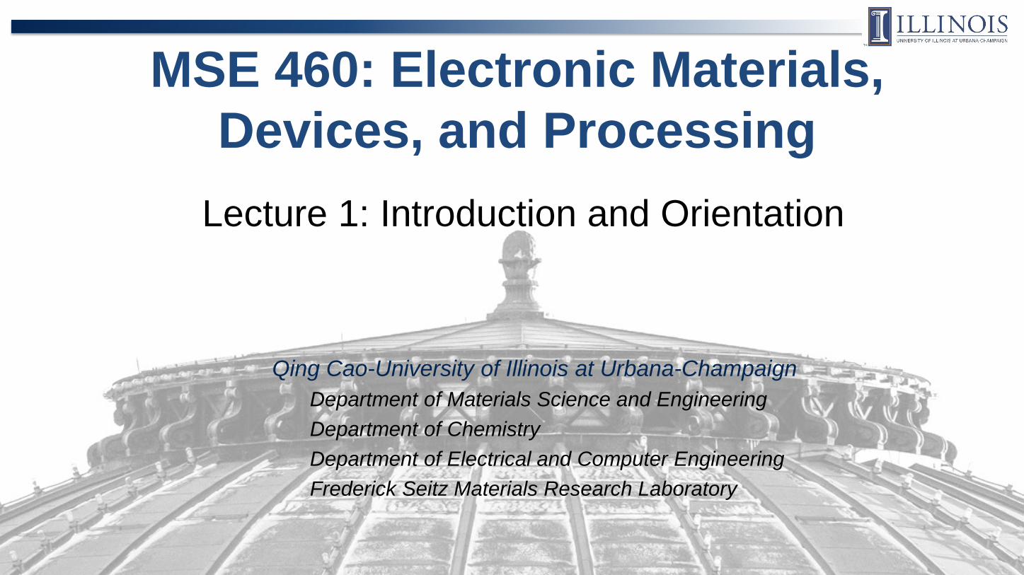
MSE 460: Electronic Materials, Devices, and Processing
Qing Cao-University of Illinois at Urbana-ChampaignDepartment of Materials Science and EngineeringDepartment of ChemistryDepartment of Electrical and Computer EngineeringFrederick Seitz Materials Research Laboratory
Lecture 1: Introduction and Orientation
2 Department of Materials Science and Engineering
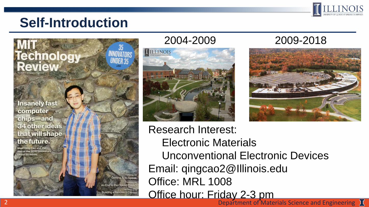
Self-Introduction2004-2009 2009-2018
Research Interest:Electronic MaterialsUnconventional Electronic Devices
Email: [email protected]: MRL 1008Office hour: Friday 2-3 pm
3 Department of Materials Science and Engineering
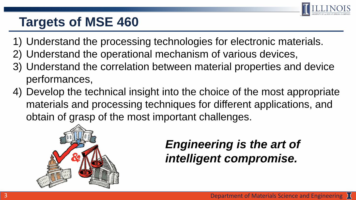
Targets of MSE 4601) Understand the processing technologies for electronic materials. 2) Understand the operational mechanism of various devices, 3) Understand the correlation between material properties and device
performances, 4) Develop the technical insight into the choice of the most appropriate
materials and processing techniques for different applications, and obtain of grasp of the most important challenges.
Engineering is the art of intelligent compromise.
4 Department of Materials Science and Engineering
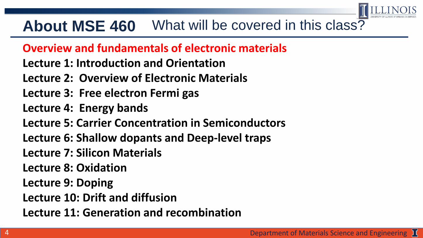
What will be covered in this class?About MSE 460Overview and fundamentals of electronic materialsLecture 1: Introduction and OrientationLecture 2: Overview of Electronic Materials Lecture 3: Free electron Fermi gas Lecture 4: Energy bands Lecture 5: Carrier Concentration in Semiconductors Lecture 6: Shallow dopants and Deep-level traps Lecture 7: Silicon Materials Lecture 8: OxidationLecture 9: DopingLecture 10: Drift and diffusion Lecture 11: Generation and recombination
5 Department of Materials Science and Engineering
About MSE 460
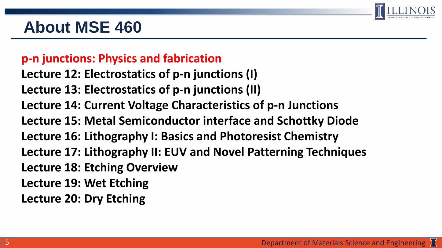
p-n junctions: Physics and fabricationLecture 12: Electrostatics of p-n junctions (I)Lecture 13: Electrostatics of p-n junctions (II)Lecture 14: Current Voltage Characteristics of p-n JunctionsLecture 15: Metal Semiconductor interface and Schottky Diode Lecture 16: Lithography I: Basics and Photoresist ChemistryLecture 17: Lithography II: EUV and Novel Patterning TechniquesLecture 18: Etching OverviewLecture 19: Wet Etching Lecture 20: Dry Etching
6 Department of Materials Science and Engineering
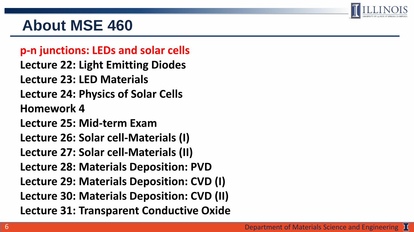
About MSE 460p-n junctions: LEDs and solar cells Lecture 22: Light Emitting DiodesLecture 23: LED MaterialsLecture 24: Physics of Solar CellsHomework 4Lecture 25: Mid-term ExamLecture 26: Solar cell-Materials (I)Lecture 27: Solar cell-Materials (II)Lecture 28: Materials Deposition: PVDLecture 29: Materials Deposition: CVD (I)Lecture 30: Materials Deposition: CVD (II)Lecture 31: Transparent Conductive Oxide
7 Department of Materials Science and Engineering
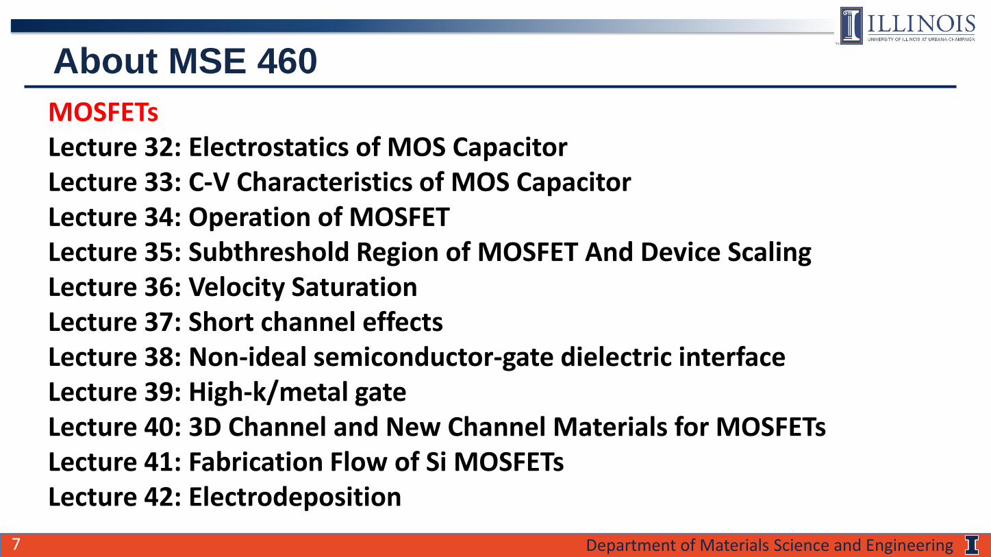
About MSE 460MOSFETsLecture 32: Electrostatics of MOS CapacitorLecture 33: C-V Characteristics of MOS Capacitor Lecture 34: Operation of MOSFETLecture 35: Subthreshold Region of MOSFET And Device Scaling Lecture 36: Velocity SaturationLecture 37: Short channel effects Lecture 38: Non-ideal semiconductor-gate dielectric interfaceLecture 39: High-k/metal gate Lecture 40: 3D Channel and New Channel Materials for MOSFETsLecture 41: Fabrication Flow of Si MOSFETsLecture 42: Electrodeposition
8 Department of Materials Science and Engineering
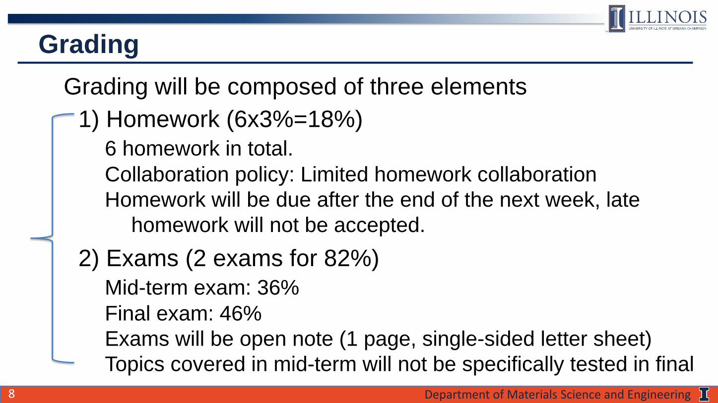
GradingGrading will be composed of three elements
1) Homework (6x3%=18%)6 homework in total. Collaboration policy: Limited homework collaborationHomework will be due after the end of the next week, late
homework will not be accepted.2) Exams (2 exams for 82%)
Mid-term exam: 36%Final exam: 46%Exams will be open note (1 page, single-sided letter sheet)Topics covered in mid-term will not be specifically tested in final
9 Department of Materials Science and Engineering
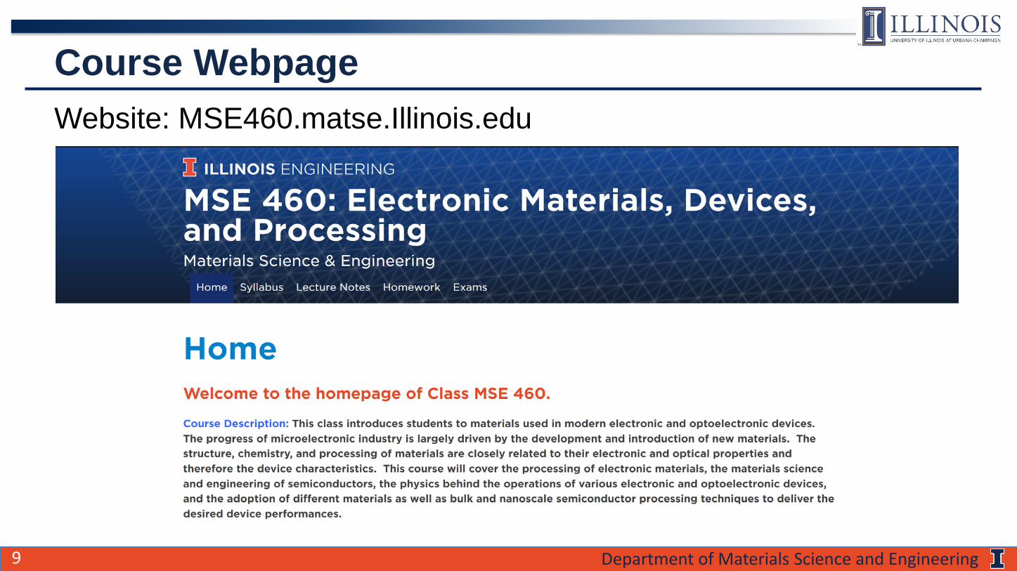
Course WebpageWebsite: MSE460.matse.Illinois.edu
10 Department of Materials Science and Engineering
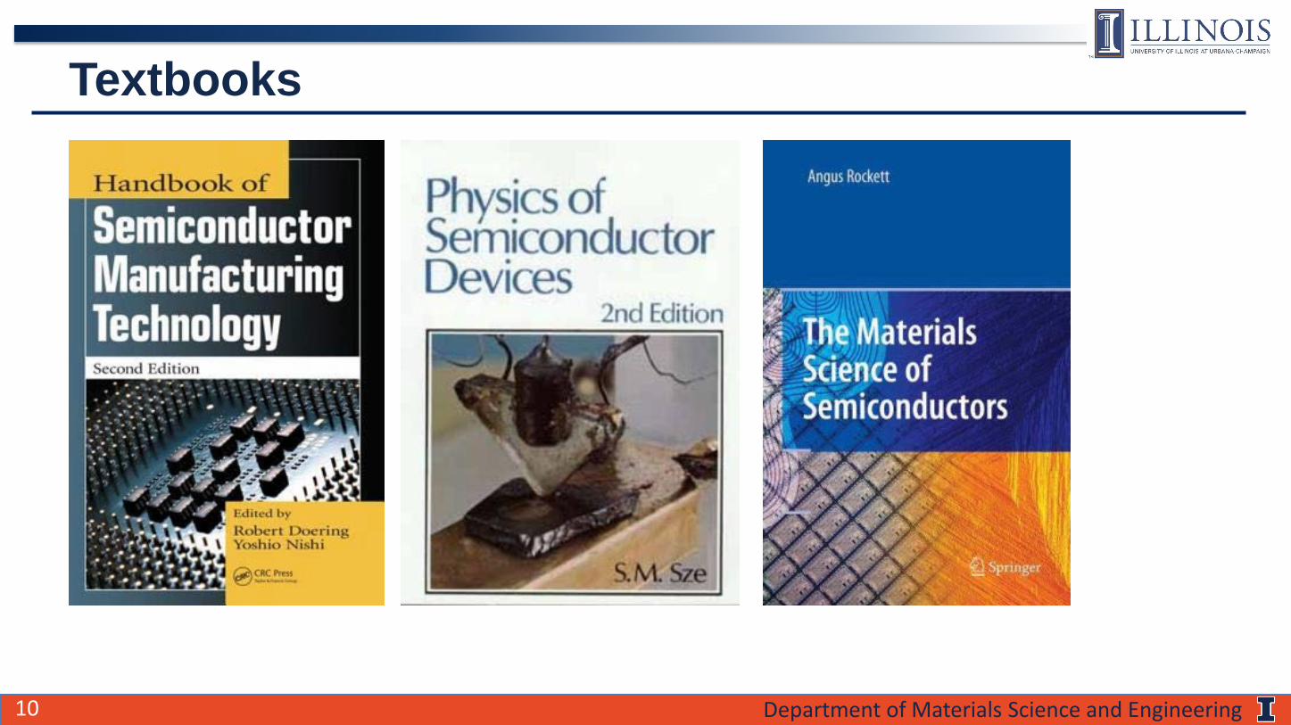
Textbooks
11 Department of Materials Science and Engineering
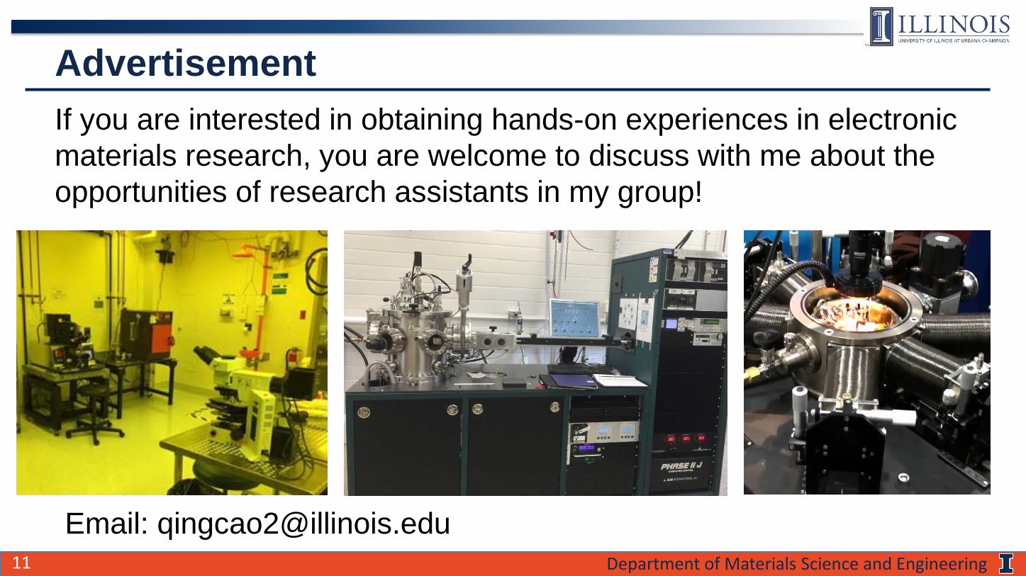
AdvertisementIf you are interested in obtaining hands-on experiences in electronic materials research, you are welcome to discuss with me about the opportunities of research assistants in my group!
Email: [email protected]
12 Department of Materials Science and Engineering
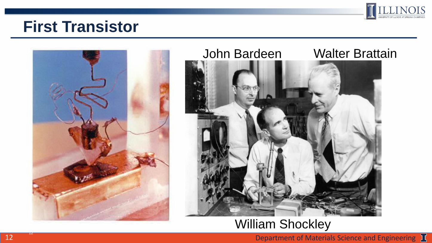
First Transistor
12
John Bardeen Walter Brattain
William Shockley
13 Department of Materials Science and Engineering
Your Motivations
13
For undergraduate students:1) Overall understanding of the field of electronic materials and
electronic devices, and make informed choices if you would like to go to graduate school.
2) Scientific knowledge of cutting edge electronics, which will make you distinct if you would like to find a job in either consulting firms or work in the public policy.
For graduate students:1) Pass the qualify exam on electronic materials2) Help you to kick start your research: know the concepts, appreciate
the problems, understand literatures, be able to communicate with you colleagues including your advisor.
14 Department of Materials Science and Engineering
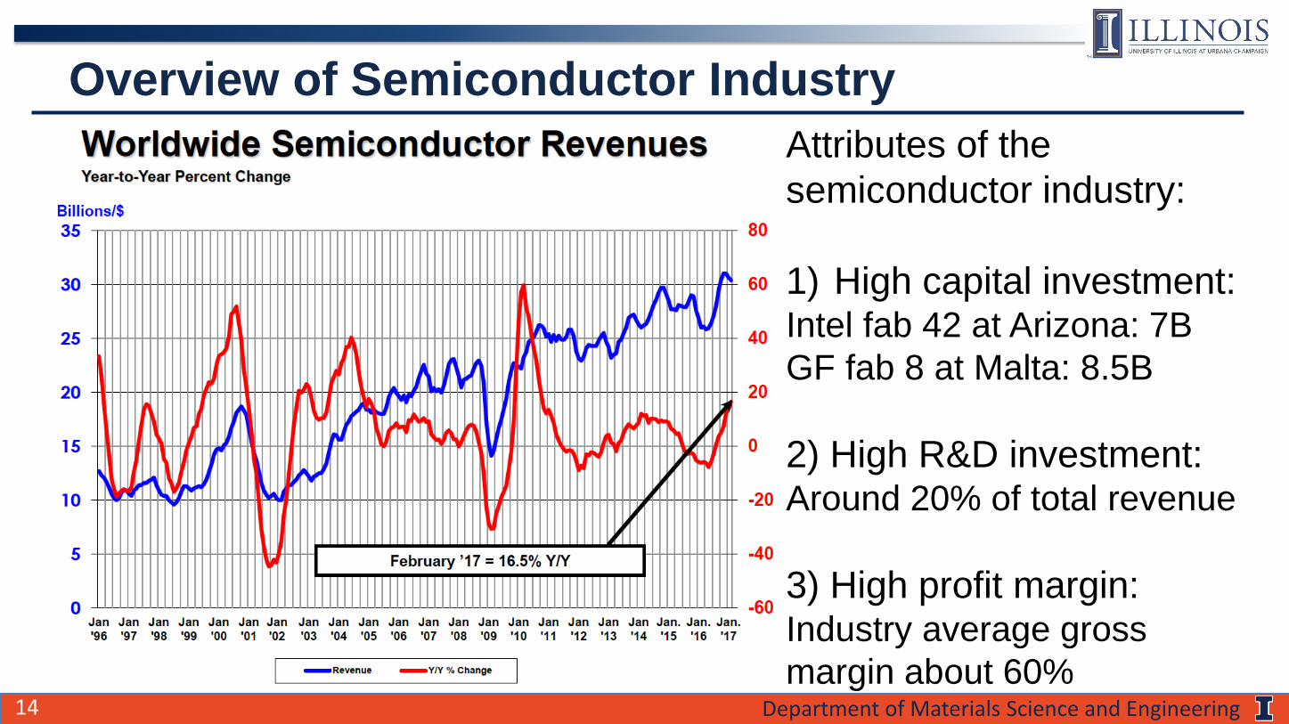
Overview of Semiconductor IndustryAttributes of the semiconductor industry:
1) High capital investment:Intel fab 42 at Arizona: 7BGF fab 8 at Malta: 8.5B
2) High R&D investment:Around 20% of total revenue
3) High profit margin:Industry average gross margin about 60%
15 Department of Materials Science and Engineering
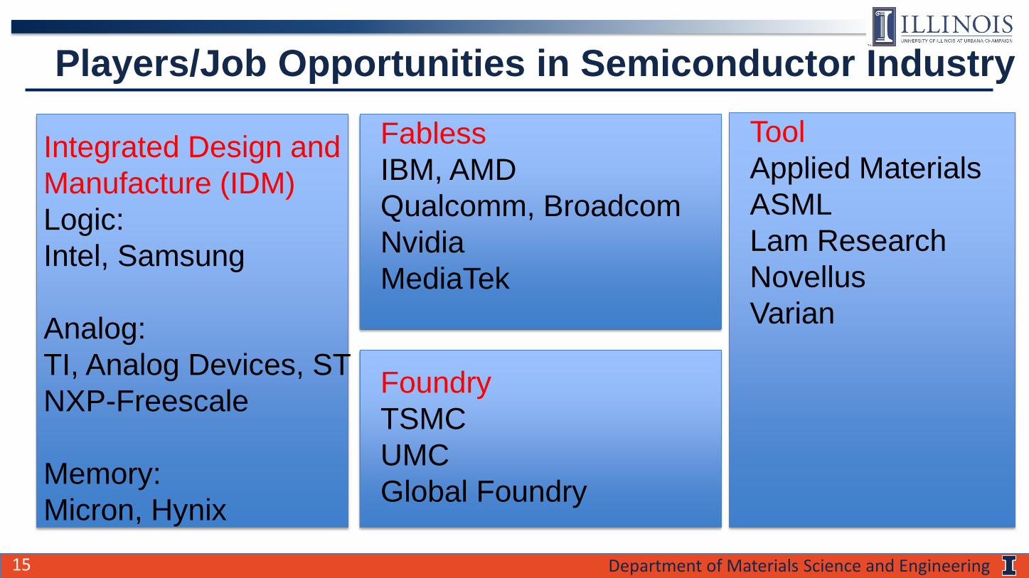
Players/Job Opportunities in Semiconductor Industry
Integrated Design and Manufacture (IDM)Logic:Intel, Samsung
Analog:TI, Analog Devices, STNXP-Freescale
Memory:Micron, Hynix
FablessIBM, AMDQualcomm, BroadcomNvidiaMediaTek
FoundryTSMCUMCGlobal Foundry
ToolApplied MaterialsASMLLam ResearchNovellusVarian

16 Department of Materials Science and Engineering
Progress in Electronics
1956 IBM SAGE computer:1MW 13,000 transistors, vacuum tubes, and diodes.
MemoryComputation
2016 Qualcomm Snapdragon 835:~1W 3B transistors.
1980 IBM 338020GB4400lbsCost: ~$0.8M
2014Sandisk512 GB0.001lbsCost: ~$200

17 Department of Materials Science and Engineering
Economic Impact
1980 85 1990 95 2000 05 2010
Wor
ld G
DP
(in T
rillio
ns)
140120
100
80
6040
200 Se
mic
ondu
ctor
Sal
es (i
n B)350
300
250
150200
100
50
0
Estimated additional value added to GDP in the last 20 years, due to the pace of innovation by Moore’s Law
18 Department of Materials Science and Engineering
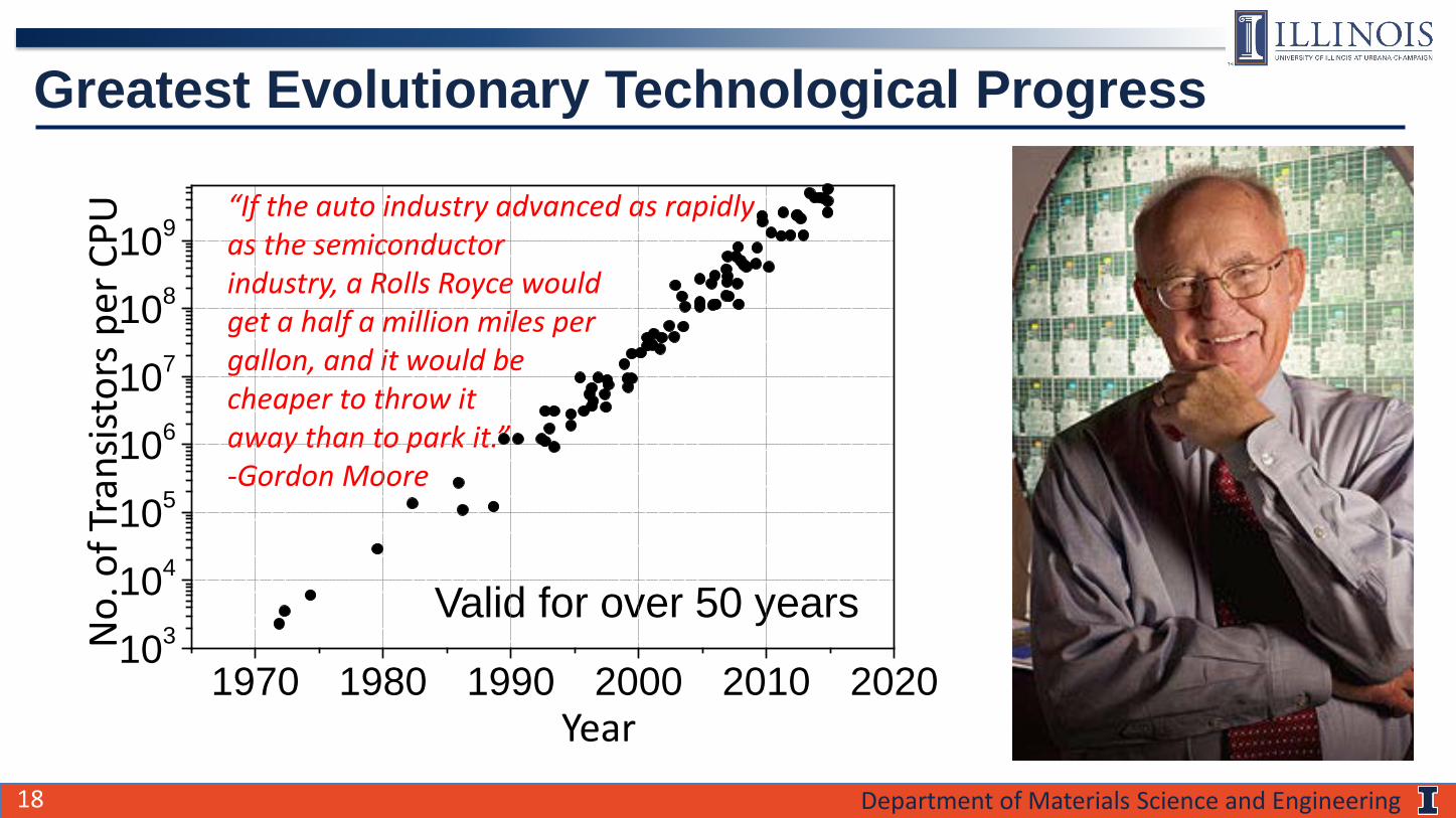
Greatest Evolutionary Technological Progress
Year
No.
of T
rans
istor
s per
CPU
Valid for over 50 years
“If the auto industry advanced as rapidly as the semiconductor industry, a Rolls Royce would get a half a million miles per gallon, and it would be cheaper to throw it away than to park it.”-Gordon Moore
1970 1980 1990 2000 2010 2020103
104
105
106
107
108
109
19 Department of Materials Science and Engineering
Fundamental Driving Forces for Semiconductor Industry
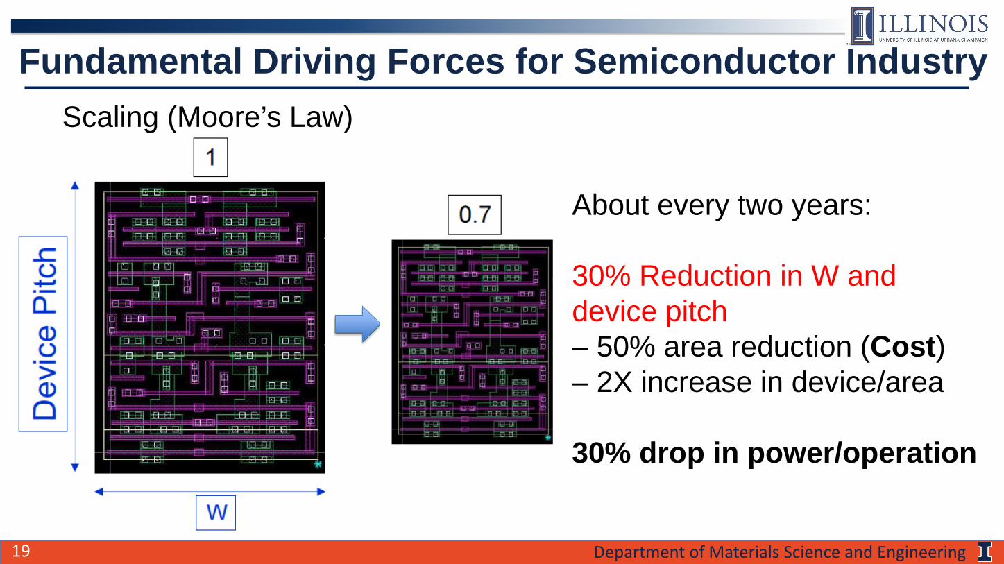
About every two years:
30% Reduction in W and device pitch– 50% area reduction (Cost)– 2X increase in device/area
30% drop in power/operation
Scaling (Moore’s Law)
20 Department of Materials Science and Engineering
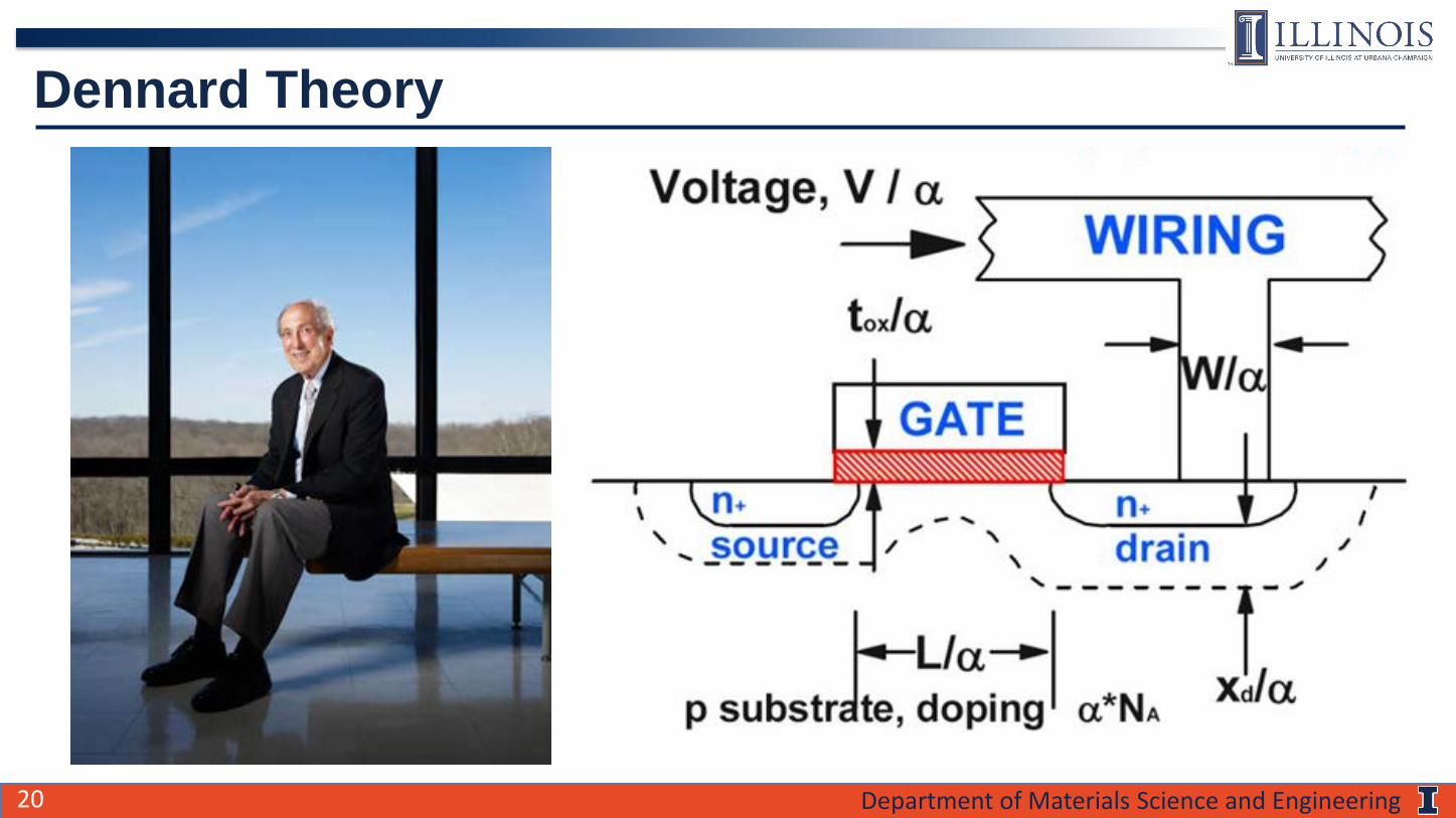
Dennard Theory
21 Department of Materials Science and Engineering
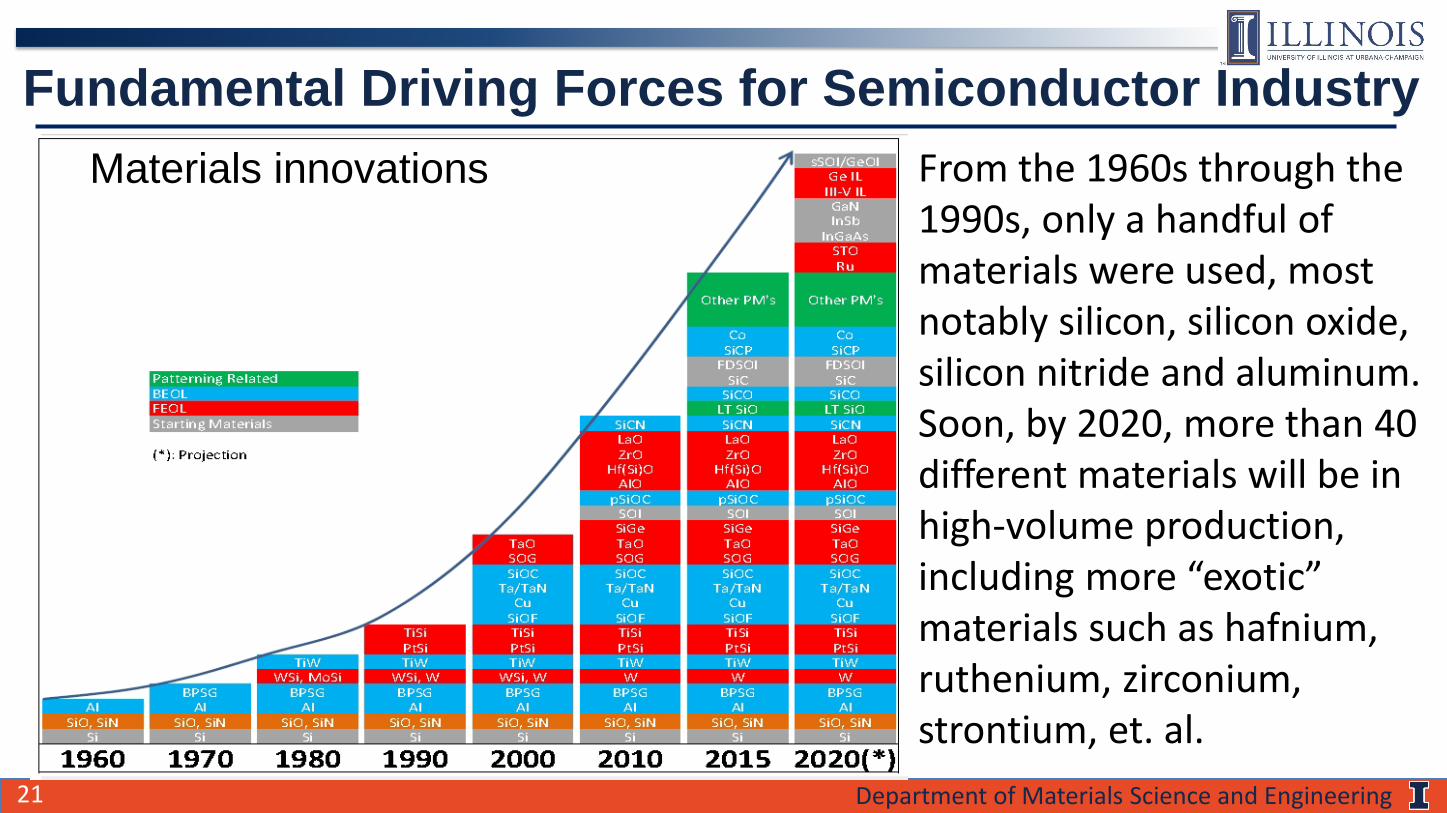
Fundamental Driving Forces for Semiconductor IndustryMaterials innovations From the 1960s through the
1990s, only a handful of materials were used, most notably silicon, silicon oxide, silicon nitride and aluminum. Soon, by 2020, more than 40 different materials will be in high-volume production, including more “exotic” materials such as hafnium, ruthenium, zirconium, strontium, et. al.
22 Department of Materials Science and Engineering
As A MatSE Class We Will Cover New pattering materials: EUV resist, di-block copolymers
New materials processing: transfer printing, additive manufacturing
New materials for LEDs and solar cells: organics, quantum dots, CdTe, CIGS, perovskite, et. al.
New materials for transistors: III-Vs, high k/metal gates, nanotubes, graphenes, 2D TMDCs, et. al.
New materials for memory: PCM, oxides/chalcogenides for memristors
23 Department of Materials Science and Engineering
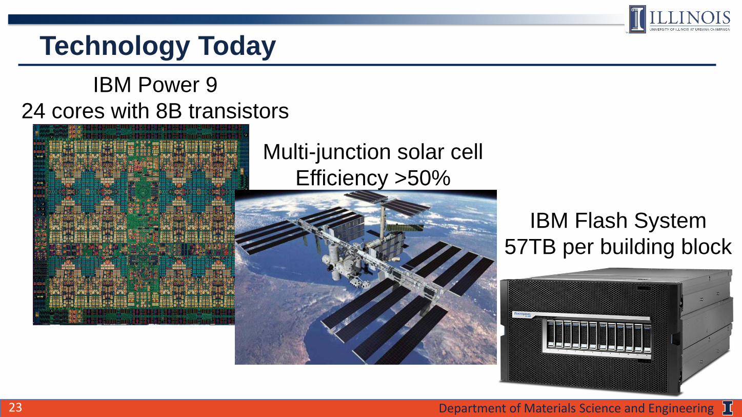
Technology Today IBM Power 9
24 cores with 8B transistors
Multi-junction solar cellEfficiency >50%
IBM Flash System57TB per building block
24 Department of Materials Science and Engineering
Challenges Ahead for Our (Your) Generation Devices for new paradigms of computingMore-Moore platform for mobile computing and IoTTechnologies for DatacentersHeterogenous integration for low power and multifunctional system-on-chipBetter solar cells for renewable energy in TW regime ……. Key enabler: New Electronic Materials
More functionalityBetter performanceLower cost
25 Department of Materials Science and Engineering
Summary
1. Logistics about MSE 4602. Overview of semiconductor industry3. Fundamental driving forces for semiconductor industry: Physical
scaling and new materials4. Current status and challenges for our (your) generation
Any Questions/Comments/Suggestions?