Embed Size (px)
Citation preview

UBI
>> Contents
Chapter 5Device Systems and Operating Modes
MSP430 Teaching Materials
Texas Instruments IncorporatedUniversity of Beira Interior (PT)
Pedro Dinis Gaspar, António Espírito Santo, Bruno Ribeiro, Humberto SantosUniversity of Beira Interior, Electromechanical Engineering Department
www.msp430.ubi.pt
Copyright 2009 Texas Instruments All Rights Reserved
www.msp430.ubi.pt

2
UBI
>> Contents Copyright 2009 Texas Instruments All Rights Reserved
www.msp430.ubi.pt
Contact bouncing

3
UBI
>> Contents Copyright 2009 Texas Instruments All Rights Reserved
www.msp430.ubi.pt
Simple debouncing Algorithm
Wenn Taste gedrückt { Zähler um 1 erhöhen
} else { Zähler auf 0 setzen
} Wenn Zähler = 5 { Aktion ausführen }

4
UBI
>> Contents Copyright 2009 Texas Instruments All Rights Reserved
www.msp430.ubi.pt
Debouncing with Counter
Uses a counter to time how long theswitch signal has been low. If the signal has been lowcontinuously for a set amount of time, then it is considered pressed and stable.
1 Setup a counter variable, initialise to zero.
2 Setup a regular sampling event, perhaps using a timer. Use a period of about 1ms

5
UBI
>> Contents Copyright 2009 Texas Instruments All Rights Reserved
www.msp430.ubi.pt
Debouncing with Shift
Similar to the first, but uses a shift registerinstead of a counter. The algorithm assumes an unsigned 8bit register value, such as that found it 8-bit microcontrollers.
1 Setup a variable to act as a shift register, initialise it to xFF.
2 Setup a regular sampling event, perhapsusing a timer. Use a period of about 1ms.
3 On a sample event: 4 Shift the variable towards the most
significant bit

6
UBI
>> Contents Copyright 2009 Texas Instruments All Rights Reserved
www.msp430.ubi.pt
Introduction
Description of the internal devices and systems of the MSP430;
It includes descriptions of the:Internal system reset;
Clock sources;
Interrupt management;
Low-power operating modes.
Quiz.

7
UBI
>> Contents Copyright 2009 Texas Instruments All Rights Reserved
www.msp430.ubi.pt7
Copyright 2008 Texas Instruments All Rights Reserved
www.msp430.ubi.pt
Interrupt management (1/8)
Interrupts:Are events applied to the application program that force a detour in program flow;
Cause CPU subprogram execution (ISR);
When Interrupt Service Routine (ISR) ends, the program flow returns to the previous state.
There are three classes of interrupts:• Reset;• Interrupts not maskable by GIE;• Interrupts maskable by GIE.

8
UBI
>> Contents Copyright 2009 Texas Instruments All Rights Reserved
www.msp430.ubi.pt
Stack Usage
9
UBI
>> Contents Copyright 2009 Texas Instruments All Rights Reserved
www.msp430.ubi.pt9
Copyright 2008 Texas Instruments All Rights Reserved
www.msp430.ubi.pt
Interrupt management (2/8)
The interrupts are used to:Allow a CPU fast response to a specific event;Avoiding continuous polling for rare events;Minimal disruption to the processing of other tasks.
In GIE-maskable interrupts, if both peripheral interrupt enable bit and GIE are set, when an interrupt is requested, it calls the ISR;
The interrupt latency time:Δt between the event beginning and the ISR execution;Interrupt latency time starts with acceptance of IR and counting until starting of first instruction of ISR.

10
UBI
>> Contents Copyright 2009 Texas Instruments All Rights Reserved
www.msp430.ubi.pt
Interrupt management (3/8)
During an interrupt event:PC of the next instruction and the SR are pushed onto the stack;Afterwards, the SR is cleared with exception of SCG0, along with the appropriate interrupt, disabling interrupts (reset the GIE flag);Other ISRs will not be called.
The RETI instruction at the end of the ISR will return to the original program flow, automatically popping the SR and PC;
Ensure that:The ISR processing time is less than the interrupt’s request time interval;To avoid stack overflow -> application program collapse.

11
UBI
>> Contents Copyright 2009 Texas Instruments All Rights Reserved
www.msp430.ubi.pt
Interrupt management (4/8)
Types of interrupts (internal and external):Reset;Interrupts not maskable by GIE: (non)-maskable interrupts (NMI);Interrupts maskable by GIE.
Interrupts priority (The nearer a module is to the CPU/NMIRS, the higher the priority).

12
UBI
>> Contents Copyright 2009 Texas Instruments All Rights Reserved
www.msp430.ubi.pt12
Copyright 2009 Texas Instruments All Rights Reserved
www.msp430.ubi.pt
Address Space
Mapped into a single, contiguous address space:All memory, including RAM, Flash/ROM, information memory, special function registers (SFRs), and peripheral registers.
Memory Map:
Memory Address Description Access End: 0FFFFh
Start: 0FFE0h Interrupt Vector Table Word/Byte
End: 0FFDFh
Flash/ROM
0F800h Start *: 01100h
Word/Byte
010FFh End *: 0107Fh Information Memory
Start: 01000h (Flash devices only) Word/Byte
End: 0FFFh Start: 0C00h
Boot Memory (Flash devices only) Word/Byte
09FFh End *: 027Fh RAM
Start: 0200h Word/Byte
End: 01FFh Start: 0100h
16-bit Peripheral modules Word
End: 00FFh Start: 0010h
8-bit Peripheral modules Byte
End: 000Fh Start: 0000h
Special Function Registers Byte

13
UBI
>> Contents Copyright 2009 Texas Instruments All Rights Reserved
www.msp430.ubi.pt13
Copyright 2009 Texas Instruments All Rights Reserved
www.msp430.ubi.pt
Interrupt vector table
Mapped at the very end of memory space (upper 16 words of Flash/ROM): 0FFE0h - 0FFFEh (4xx devices);Priority of the interrupt vector increases with the word address.

14
UBI
>> Contents Copyright 2009 Texas Instruments All Rights Reserved
www.msp430.ubi.pt
IRQ Handling in „C“

15
UBI
>> Contents Copyright 2009 Texas Instruments All Rights Reserved
www.msp430.ubi.pt
Interrupt management (5/8)
Types of interrupts (internal and external):
Main differences between non-maskable and maskableinterrupts:• Non-maskable interrupts cannot be disabled by the GIE
bit of the SR. Used for high priority events e.g. emergency shutdown;
• Maskable interrupts are recognized by the CPU’s interrupt control, so the GIE bit must be set. Can be switched off by software.
The system reset interrupts (Oscillator/Flash and the Hard Reset) are treated as highest priority non-maskableinterrupts, with their own interrupt vectors.

16
UBI
>> Contents Copyright 2009 Texas Instruments All Rights Reserved
www.msp430.ubi.pt
Interrupt management (6/8)
Types of interrupts (internal and external):Non Maskable Interrupts:• Not masked by GIE;• Enabled by individual interrupt enable bits;
• Depend on the event source:– NMIIE: Non-Maskable Interrupts Interrupt Enable:
» RST/NMI is configured in NMI mode;» WDTNMIES bit generates an NMI;» The RST/NMI flag NMIIFG is also set.
– ACCVIE: ACCess Violation to the flash memory Interrupt Enable:» The flash ACCVIFG flag is set.
– OFIE: Oscillator Fault Interrupt Enable:» This signal can be triggered by a PUC signal.

17
UBI
>> Contents Copyright 2009 Texas Instruments All Rights Reserved
www.msp430.ubi.pt
Introduction (1/3)
Up to ten 8-bit digital Input/Output (I/O) ports, P1 to P10 (depending on the MSP430 device);
I/O ports P1 and P2 have interrupt capability;
Each interrupt for these I/O lines can be individually configured:
To provide an interrupt on a rising or falling edge;All interruptible I/O lines source a single interrupt vector.
The available digital I/O pins for the hardware development tools:
eZ430-F2013: 10 pins - Port P1 (8 bits) and Port P2 (2 bits);eZ430-RF2500: 32 pins - Port P1 to P4 (8 bits);Experimenter’s board: 80 pins – Port P1 to P10 (8 bits).

18
UBI
>> Contents Copyright 2009 Texas Instruments All Rights Reserved
www.msp430.ubi.pt
Introduction (2/3)
Each I/O port can be:
Programmed independently for each bit;
Combine input, output, and interrupt functionality;
Edge-selectable input interrupt capability for all 8 bits of ports P1 and P2;
Read/write access to port-control registers is supported by all two- or one-address instructions;
Individually programmable pull-up/pull-down resistor (2xx family only).

19
UBI
>> Contents Copyright 2009 Texas Instruments All Rights Reserved
www.msp430.ubi.pt
Introduction (3/3)
The port pins can be individually configured as I/O for special functions, such as:
USART – Universal Synchronous/Asynchronous Receive/Transmit for serial data;
Input comparator for analogue signals;
Analogue-to-Digital converter;
Others functions (see specific datasheet for details).

20
UBI
>> Contents Copyright 2009 Texas Instruments All Rights Reserved
www.msp430.ubi.pt
Registers (1/6)
Independent of the I/O port type (non-interruptible orinterruptible), the operation of the ports is configuredby user software, as defined by the following registers:
Direction Registers (PxDIR):• Read/write 8-bit registers;• Select the direction of the corresponding I/O pin,
regardless of the selected function of the pin (general purpose I/O or as a special function I/O);
• For other module functions, must be set as required by the other function.
• PxDIR configuration:Bit = 1: the individual port pin is set as an output;Bit = 0: the individual port pin is set as an input.

21
UBI
>> Contents Copyright 2009 Texas Instruments All Rights Reserved
www.msp430.ubi.pt
Registers (2/6)
Input Registers (PxIN):• When pins are configured as GPIO, each bit of these
read-only registers reflects the input signal at the corresponding I/O pin;
• PxIN configuration:Bit = 1: The input is high;Bit = 0: The input is low;
• Tip: Avoid writing to these read-only registers because it will result in increased current consumption.

22
UBI
>> Contents Copyright 2009 Texas Instruments All Rights Reserved
www.msp430.ubi.pt
Registers (3/6)
Output Registers (PxOUT):• Each bit of these registers reflects the value written to
the corresponding output pin.
• PxOUT configuration:Bit = 1: The output is high;Bit = 0: The output is low.
– Note: the PxOUT Register is read-write. This means that the previous value written to it can be read back and modified to generate the next output signal.

23
UBI
>> Contents Copyright 2009 Texas Instruments All Rights Reserved
www.msp430.ubi.pt
Registers (4/6)
Pull-up/down Resistor Enable Registers (PxREN):
• Only available for the 2xx family;• Each bit of this register enables or disables the pull-
up/pull-down resistor of the corresponding I/O pin.
• PxREN configuration:– Bit = 1: Pull-up/pull-down resistor enabled;– Bit = 0: Pull-up/pull-down resistor disabled.
– When pull-up/pull-down resistor is enabled:– In this case Output Registers (PxOUT) select:
» Bit = 1: The pin is pulled up;» Bit = 0: The pin is pulled down.

24
UBI
>> Contents Copyright 2009 Texas Instruments All Rights Reserved
www.msp430.ubi.pt
Registers (5/6)
Function Select Registers: (PxSEL) and (PxSEL2):
• Some port pins are multiplexed with other peripheral module functions (see the device-specific datasheet);
• These bits: PxSEL and PxSEL2 (see specific device datasheet), are used to select the pin function:– I/O general purpose port;– Peripheral module function.
• PxSEL configuration:Bit = 0: I/O Function is selected for the pin;Bit = 1: Peripheral module function enabled for pin.

25
UBI
>> Contents Copyright 2009 Texas Instruments All Rights Reserved
www.msp430.ubi.pt
Registers (6/6)
Function Select Registers: (PxSEL) and (PxSEL2):
• The 2xx family of devices provide the PxSEL2 bit to configure additional features of the device;
• The PxSEL and PxSEL2 bits in combination provide the following configuration:– Bit = 0: I/O function is selected for the pin;– Bit = 1: Peripheral module function is selected for
the pin.
Selects the secondary peripheral module function11Reserved (See device-specific data sheet)01
Selects the primary peripheral module function10Selects general purpose I/O function00
Pin FunctionPxSEL2PxSEL
Note: P1 and P2 configured as peripheral module function (PxSEL = 1 and/or PxSEL2) -> interrupts disabled.

26
UBI
>> Contents Copyright 2009 Texas Instruments All Rights Reserved
www.msp430.ubi.pt
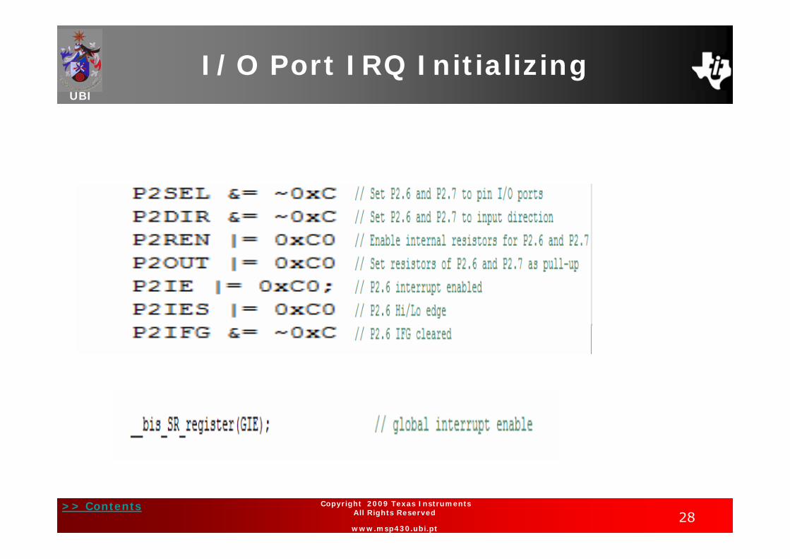
Interruptible ports (P1 and P2) (1/2)
Each pin of ports P1 and P2 is able to make an interrupt request;
Pins are configured with additional registers:
Interrupt Enable (PxIE):• Read-write register to enable interrupts on individual pins;
• PxIE configuration:Bit = 1: The interrupt is enabled;Bit = 0: The interrupt is disabled.
• Each PxIE bit enables the interrupt request associated with the corresponding PxIFG interrupt flag;
• Writing to PxOUT and/or PxDIR can result in setting PxIFG.

27
UBI
>> Contents Copyright 2009 Texas Instruments All Rights Reserved
www.msp430.ubi.pt
Interruptible ports (P1 and P2) (2/2)
Interrupt Edge Select Registers (PxIES):• Selects the transition on which an interrupt occurs (if PxIE
and GIE are set);
• PxIES configuration:Bit = 1: Interrupt flag is set on a high-to-low transition;Bit = 0: Interrupt flag is set on a low-to-high transition.
Interrupt Flag Registers (PxIFG)• Set automatically when an the programmed signal
transition (edge) occurs;• PxIFG flag can be set and must be reset by software.
• PxIFG configuration:Bit = 0: No interrupt is pending;Bit = 1: An interrupt is pending.
28
UBI
>> Contents Copyright 2009 Texas Instruments All Rights Reserved
www.msp430.ubi.pt
I/O Port IRQ Initializing

29
UBI
>> Contents Copyright 2009 Texas Instruments All Rights Reserved
www.msp430.ubi.pt
Interrupt management (7/8)
Types of interrupts (internal and external):Non Maskable Interrupts:• Example: ACCVIE (2xx family).ACCV=1 → ACCVIFG=1ACCVIFG=1 and ACCVIE=1 (set by software) → NMIRS=1

30
UBI
>> Contents Copyright 2009 Texas Instruments All Rights Reserved
www.msp430.ubi.pt
Interrupt management (8/8)
Types of interrupts (internal and external):
(by GIE) Maskable Interrupts:
• Peripherals with interrupt capability or the watchdog timer overflow in interval timer mode;
• Individual enable/disable flag, located in peripheral registers or in the individual module;
• Can be disabled by resetting the GIE bit in SR, either by software or by hardware/interrupt.

31
UBI
>> Contents Copyright 2009 Texas Instruments All Rights Reserved
www.msp430.ubi.pt
System clocks (1/24)
Allows the CPU and peripherals to operate from different clock sources;
The system clocks depend on the device in the MSP430 family:
MSP430x2xx:• The Basic Clock Module+ (BCM+);
– One or two oscillators (depending on the device);– Capable of working with external crystals or
resonators;– Internal digitally controlled oscillator (DCO);– Working frequency to up 16 MHz;– Lower power consumption;– Lower internal oscillator start-up time.

32
UBI
>> Contents Copyright 2009 Texas Instruments All Rights Reserved
www.msp430.ubi.pt
System clocks (2/24)
MSP430x2xx:• Basic Clock+:

33
UBI
>> Contents Copyright 2009 Texas Instruments All Rights Reserved
www.msp430.ubi.pt
System clocks (3/24)
MSP430x4xx:• Frequency Locked Loop (FLL+):
– One or two oscillators (depending on the device);
– Capable of working with external crystals or resonators;
– Internal digitally controlled oscillator (DCO), adjusted and controlled by hardware;
– Synchronized to a high-frequency internal clock from a low frequency external oscillator.

34
UBI
>> Contents Copyright 2009 Texas Instruments All Rights Reserved
www.msp430.ubi.pt
System clocks (4/24)
MSP430x4xx:• FLL+:

35
UBI
>> Contents Copyright 2009 Texas Instruments All Rights Reserved
www.msp430.ubi.pt
System clocks (5/24)
The clock sources from these oscillators can be selected to generate different clock signals:
Master clock (MCLK):• Generated by DCO (but can also be fed by the crystal
oscillator);• Activate and stable in less than 6 μsec;• Used by the CPU and high-speed peripherals.
Subsystem main clock (SMCLK):• Used as alternative clock source for peripherals.
Auxiliary clock (ACLK):• RTC self wake-up function from low power modes (32.768
kHz);• Always fed by the crystal oscillator.
Each clock can be internally divided by a factor of 1, 2, 4 or 8.

36
UBI
>> Contents Copyright 2009 Texas Instruments All Rights Reserved
www.msp430.ubi.pt
System clocks (6/24)
Low/High frequency oscillator (LFXT1):Implemented in all MSP430 devices;
Used with either:• Low-frequency 32.768 kHz watch crystals (RTC);• Standard crystals, resonators, or external clock sources
in range 450 kHz to 8 MHz (16 MHz in 2xx family).
The operating mode selection (one bit):• (=0) -> LF clock;• (=1) -> HF clock.
• XTS: located at the BCSCTL1 register (2xx family);• XTS_FLL: located at the FLL_CTL0 register (4xx family).

37
UBI
>> Contents Copyright 2009 Texas Instruments All Rights Reserved
www.msp430.ubi.pt
System clocks (7/24)
Second crystal oscillator (XT2):Sources of XT2CLK and its characteristics are identical to LFXT1 in HF mode (range 450 kHz to 8 MHz, or 16 MHz in the 2xx family);
Load capacitance for the high frequency crystal or resonator must be provided externally;
This oscillator can be disabled by the XT2OFF bit:• BCSCTL1 register in 2xx family;• FLL_CTL1 register in 4xx family (if XT2CLK is unused
for source the MCLK and SMCLK clock signals).

38
UBI
>> Contents Copyright 2009 Texas Instruments All Rights Reserved
www.msp430.ubi.pt
System clocks (8/24)
Digitally-controlled oscillator (DCO):Integrated ring oscillator with RC-type characteristics;
Provide a wide, software-controllable frequency range;
DCO frequency is synchronized to the FLL;
Frequency modulation method provided by FLL functionality:
• 2xx family:– Does not have full FLL functionality;– The DCO generates an internal signal (DCOCLK):
» Programmed internally or externally (DCOR bit);» Controlled by a resistor connected to the ROSC
and VCC pins.

39
UBI
>> Contents Copyright 2009 Texas Instruments All Rights Reserved
www.msp430.ubi.pt
System clocks (9/24)
• 2xx family:– The DCO control bits:
» RSELx: fDCO range selection;
» DCOx: fDCO defined by the RSEL bits. The step size is defined by the parameter SDCO;
» MODx: Modulation bits select how often fDCO(RSEL, DCO+1) is used within the period of 32 DCOCLK cycles.
» The frequency fDCO(RSEL, DCO) is used for the remaining cycles.
– Specific frequency ranges and values vary by device:
( ) )1,(),(
)1,(),(
3232
+
+
×−+×
××=
DCORSELDCODCORSELDCO
DCORSELDCODCORSELDCOavg fMODfMOD
fff

40
UBI
>> Contents Copyright 2009 Texas Instruments All Rights Reserved
www.msp430.ubi.pt
System clocks (10/24)
• 2xx family:– Basic Clock Module+ (BCM+) registers configuration:
» DCOCTL: DCO Control Register
MODxDCOx
01234567
Modulator selection.MODx4-0
Discrete DCO frequency selection step (depends on RSELx bits).DCOx7-5
DescriptionBit

41
UBI
>> Contents Copyright 2009 Texas Instruments All Rights Reserved
www.msp430.ubi.pt
System clocks (11/24)
• 2xx family:– Basic Clock Module+ (BCM+) registers configuration:
» BCSCTL1: Basic Clock System Control Reg. 1
RSELxDIVAxXTSXT2OF
01234567
Range select. Sixteen different frequency ranges are available.RSELx3-0
ACLK frequency divider:DIVA1 DIVA0 = 0 0 ⇒ /1DIVA1 DIVA0 = 0 1 ⇒ /2DIVA1 DIVA0 = 1 0 ⇒ /4DIVA1 DIVA0 = 1 1 ⇒ /8
DIVAx5-4
LFXT1 oscillator operating mode:XTS = 0 ⇒ LF mode (low frequency)XTS = 1 ⇒ HF mode (high frequency)
XTS6
XT2 oscillator fault:XT2OF = 0 ⇒ XT2 normal operationXT2OF = 1 ⇒ XT2 fault condition
XT2OF7
DescriptionBit

42
UBI
>> Contents Copyright 2009 Texas Instruments All Rights Reserved
www.msp430.ubi.pt
System clocks (12/24)
• 2xx family:– Basic Clock Module+ (BCM+) registers configuration:
» BCSCTL2: Basic Clock System Control Reg. 2
DCORDIVSxSELSDIVMxSELMx
01234567
DCO resistor selector DCOR = 0 ⇒ Internal resistorDCOR = 1 ⇒ External resistor
DCOR0
SMCLK frequency divider: DIVS1 DIVS0 = 0 0 ⇒ /1DIVS1 DIVS0 = 0 1 ⇒ /2DIVS1 DIVS0 = 1 0 ⇒ /4DIVS1 DIVS0 = 1 1 ⇒ /8
DIVSx2-1
SMCLK source: SELS = 0 ⇒ DCOSELS = 1 ⇒ XT2
SELS3
MCLK frequency divider: DIVM1 DIVM0 = 0 0 ⇒ /1DIVM1 DIVM0 = 0 1 ⇒ /2DIVM1 DIVM0 = 1 0 ⇒ /4DIVM1 DIVM0 = 1 1 ⇒ /8
DIVMx5-4
MCLK source: SELM1 SELM0 = 0 0 ⇒ DCOSELM1 SELM0 = 0 1 ⇒ DCOSELM1 SELM0 = 1 0 ⇒ XT2SELM1 SELM0 = 1 1 ⇒ LFXT1
SELMx7-6
DescriptionBit

43
UBI
>> Contents Copyright 2009 Texas Instruments All Rights Reserved
www.msp430.ubi.pt
System clocks (13/24)
• 2xx family:– Basic Clock Module+ (BCM+) registers configuration:
» BCSCTL3: Basic Clock System Control Reg. 3
LFXT1OFXT2OFFXCAPxLFXT1SxXT2Sx
01234567
LFXT1OF oscillator fault: LFXT1OF = 0 ⇒ No fault conditionLFXT1OF = 1 ⇒ Fault condition
LFXT1OF0
XT2 oscillator fault: XT2OFF = 0 ⇒ No fault conditionXT2OFF = 1 ⇒ Fault condition
XT2OFF1
Oscillator capacitor selection: XCAP1 XCAP0 = 0 0 ⇒ ~1 pFXCAP1 XCAP0 = 0 1 ⇒ ~6 pFXCAP1 XCAP0 = 1 0 ⇒ ~10 pFXCAP1 XCAP0 = 1 1 ⇒ ~12.5 pF
XCAPx3-2
Low-frequency clock select and LFXT1 range select: XTS=0: XTS=1:LFXT1S1 LFXT1S0 = 0 0 ⇒ 32768 Hz 0.4 - 1-MHzLFXT1S1 LFXT1S0 = 0 1 ⇒ Reserved 1 - 3-MHzLFXT1S1 LFXT1S0 = 1 0 ⇒ VLOCLK 3 - 16-MHzLFXT1S1 LFXT1S0 = 1 1 ⇒ External 0.4 - 16-MHz
LFXT1Sx5-4
XT2 range select: XT2S1 XT2S0 = 0 0 ⇒ 0.4 – 1 MHzXT2S1 XT2S0 = 0 1 ⇒ 1 – 3 MHzXT2S1 XT2S0 = 1 0 ⇒ 3 – 16 MHzXT2S1 XT2S0 = 1 1 ⇒ 0.4 – 16-MHz (Digital external)
XT2Sx7-6
DescriptionBit

44
UBI
>> Contents Copyright 2009 Texas Instruments All Rights Reserved
www.msp430.ubi.pt
System clocks (14/24)
• 4xx family:– The DCO generates the signal:
(fDCOCLK)=ACLK x D x (N+1).
– The DCOPLUS bit sets the fDCOCLK frequency to:» fDCO;» fDCO/D: The FLLDx bits configure D=1, 2, 4 or 8.
– By default, DCOPLUS = 0, D = 2 providing:» fDCO/2 on fDCOCLK;» The multiplier (N+1) and D set the fDCOCLK.
– DCOPLUS = 0: fDCOCLK = (N + 1) x fACLK– DCOPLUS = 1: fDCOCLK = D x (N + 1) x fACLK
– fDCO range selected by FNx bits (register SCFI0).

45
UBI
>> Contents Copyright 2009 Texas Instruments All Rights Reserved
www.msp430.ubi.pt
System clocks (15/24)
Frequency Locked Loop (FLL) - 4xx family:Automatically modulates the DCO frequency;Greater precision and control;Mixes the programmed fDCO with the next higher fDCO.
Operation:• The DCO signal is divided by D and divided by N+1;• The signal obtained is continuously applied to the count
down input of a 10-bit up/down counter (frequency integrator);
• ACLK (LFXT1) is applied to the count up input of the counter;
• The counter output is fed back to the DCO modulator, correcting and synchronizing the operating frequency;
• The output of the frequency integrator can be read in SCFI1 and SCFI0 registers;
• The count is adjusted by +1 each ACLK (xtal) period, by -1 each period of the divided DCO signal.

46
UBI
>> Contents Copyright 2009 Texas Instruments All Rights Reserved
www.msp430.ubi.pt
System clocks (16/24)
Frequency Locked Loop (FLL) - 4xx family:29 fDCO taps are set by 5 of the integrator bits, SCFI1 bits 7 to 3 (28, 29, 30, and 31 are equivalent);
Each tap is approximately 10% higher than the previous;
The modulator mixes two adjacent DCO frequencies to produce fractional taps;
SCFI1 register bits 2 to 0 and SCFI0 register bits 1 to 0 are used for the digital modulator;
The method of FLL can be described as switching between the two most close neighbour frequencies to our frequency asked for to achieve the frequency requested as a time-weighted average of both frequencies.

47
UBI
>> Contents Copyright 2009 Texas Instruments All Rights Reserved
www.msp430.ubi.pt
System clocks (17/24)
Frequency Locked Loop (FLL) - 4xx family:FLL+ clock module configuration:• SCFQCTL: System Clock Control Register
NSCFQ_M
01234567
DCO frequency multiplier factor:DCOPLUS = 0 ⇒ fDCOCLK = (N +1) fcrystalDCOPLUS = 1 ⇒ fDCOCLK = D (N +1) fcrystal
N6-0
Modulation control:SCFQ_M = 0 ⇒ FLL modulation enable SCFQ_M = 1 ⇒ FLL modulation disable
SCFQ_M7
DescriptionBit

48
UBI
>> Contents Copyright 2009 Texas Instruments All Rights Reserved
www.msp430.ubi.pt
System clocks (18/24)
Frequency Locked Loop (FLL) - 4xx family:FLL+ clock module configuration:• SCFI0: System Clock Frequency Integrator Reg. 0
MODx (LSBs)FN_xFLLDx
01234567
LSB modulator bits modified by the FLL+.MODx1-0
fDCO operating range:0000 ⇒ 0.65 – 6.1 MHz0001 ⇒ 1.3 – 12.1 MHz001x ⇒ 2.0 – 17.9 MHz01xx ⇒ 2.8 – 26.6 MHz1xxx ⇒ 4.2 – 46.0 MHz
FN_x5-2
FLL+ feedback loop fDCOCLK divider:FLLD1 FLLD0 = 0 0 ⇒ /1FLLD1 FLLD0 = 0 1 ⇒ /2FLLD1 FLLD0 = 1 0 ⇒ /4FLLD1 FLLD0 = 1 1 ⇒ /8
FLLDx7-6
DescriptionBit

49
UBI
>> Contents Copyright 2009 Texas Instruments All Rights Reserved
www.msp430.ubi.pt
System clocks (19/24)
Frequency Locked Loop (FLL) - 4xx family:FLL+ clock module configuration:• SCFI1: System Clock Frequency Integrator Reg. 1
MODx (MSBs)DCOx
01234567
MSB modulator bits modified by the FLL+.MODx2-0
DCO tap selection modified by the FLL+.DCOx7-3
DescriptionBit

50
UBI
>> Contents Copyright 2009 Texas Instruments All Rights Reserved
www.msp430.ubi.pt
System clocks (20/24)
Frequency Locked Loop (FLL) - 4xx family:FLL+ clock module configuration:• FLL_CTL0: FLL+ Control Register 0
DCOFLFOFXT1OFXT2OFXCAPxPFXTS_FLLDCOPLUS
01234567
DCO oscillator fault: DCOF = 0 ⇒ DCO normal operationDCOF = 1 ⇒ DCO fault condition
DCOF0
LF mode LFXT1 oscillator fault: LFOF = 0 ⇒ LFXT1 normal operationLFOF = 1 ⇒ LFXT1 fault condition
LFOF1
HF mode LFXT1 oscillator fault: XT1OF = 0 ⇒ LFXT1 normal operationXT1OF = 1 ⇒ LFXT1 fault condition
XT1OF2
XT2 oscillator fault: XT2OF = 0 ⇒ XT2 normal operationXT2OF = 1 ⇒ XT2 fault condition
XT2OF3
LFXT1 oscillator load capacitance: XCAP1PF XCAP0PF = 0 0 ⇒ ∼ 1 pFXCAP1PF XCAP0PF = 0 1 ⇒ ∼ 6 pFXCAP1PF XCAP0PF = 1 0 ⇒ ∼ 8 pFXCAP1PF XCAP0PF = 1 1 ⇒ ∼ 10 pF
XCAPxPF5-4
LFXT1 oscillator operating mode: XTS_FLL = 0 ⇒ LF mode (low frequency)XTS_FLL = 1 ⇒ HF mode (high frequency)
XTS_FLL6
DCO output pre-divider: DCOPLUS = 0 ⇒ Divider enableDCOPLUS = 1 ⇒ Divider disable
DCOPLUS7
DescriptionBit

51
UBI
>> Contents Copyright 2009 Texas Instruments All Rights Reserved
www.msp430.ubi.pt
System clocks (21/24)
Frequency Locked Loop (FLL) - 4xx family:FLL+ clock module configuration:• FLL_CTL1: FLL+ Control Register 0
FLL_DIVxSELSSELMxXT2OFFSMCLKOFF-
01234567
ACLK frequency divider: FLL_DIV_0 = 0 0 ⇒ /1FLL_DIV_1 = 0 1 ⇒ /2FLL_DIV_2 = 1 0 ⇒ /4FLL_DIV_3 = 1 1 ⇒ /8
FLL_DIVx1-0
SMCLK source: SELS = 0 ⇒ DCOSELS = 1 ⇒ XT2
SELS2
MCLK source: SELM1 SELM0 = 0 0 ⇒ DCOSELM1 SELM0 = 0 1 ⇒ DCOSELM1 SELM0 = 1 0 ⇒ XT2SELM1 SELM0 = 1 1 ⇒ LFXT1
SELMx4-3
XT2 disable: XT2OFF = 0 ⇒ XT2 enableXT2OFF = 1 ⇒ XT2 disable
XT2OFF5
SMCLK disable: SMCLKOFF = 0 ⇒ SMCLK enableSMCLKOFF = 1 ⇒ SMCLK disable
SMCLKOFF6
DescriptionBit

52
UBI
>> Contents Copyright 2009 Texas Instruments All Rights Reserved
www.msp430.ubi.pt
System clocks (22/24)
Internal clock signals:In 2xx family clock system = the basic clock module+:• Support for a 32768 Hz watch crystal oscillator;• Internal very-low-power low-frequency oscillator;• Internal digitally-controlled oscillator (DCO) stable <1 μs.
The BCM+ provides the following clock signals:– Auxiliary clock (ACLK), sourced either from:
» 32768 Hz watch crystal;» Internal oscillator LFXT1CLK in LF mode with an
internal load capacitance of 6 pF.
– Main clock (MCLK), the system clock used by the CPU;
– Sub-Main clock (SMCLK), the sub-system clock used by the peripheral modules.

53
UBI
>> Contents Copyright 2009 Texas Instruments All Rights Reserved
www.msp430.ubi.pt
System clocks (23/24)
Internal clock signals:Both MCLK and SMCLK are sourced from DCOCLK at ~1.1 MHz but can be sourced up to 16 MHz;
2xx DCO calibration data (in flash info memory segment A).
010F9h010F8h
ByteByte
CALBC1_16MHZCALBC0_16MHZ16 MHz
010FBh010FAh
ByteByte
CALBC1_12MHZCALBC0_12MHZ12 MHz
010FDh010FCh
ByteByte
CALBC1_8MHZCALBC0_8MHZ8 MHz
010FFh010FEh
ByteByte
CALBC1_1MHZCALBC0_1MHZ1 MHz
AddressSizeCalibration registerDCO frequency

54
UBI
>> Contents Copyright 2009 Texas Instruments All Rights Reserved
www.msp430.ubi.pt
System clocks (24/24)
Internal clock signals:Electrical characteristics vary over the recommended supply voltage range of between 2.2 V and 3.6 V. Higher DCO frequencies require higher supply voltages.Typical characteristics in active mode supply current for the (2xx family):

55
UBI
>> Contents Copyright 2009 Texas Instruments All Rights Reserved
www.msp430.ubi.pt
Low power operating modes (1/11)
One of the main features of the MSP430 families:Low power consumption (about 1 mW/MIPS or less);
Important in battery operated embedded systems.
Low power consumption is only accomplished:Using low power operating modes design;
Depends on several factors such as:• Clock frequency;• Ambient temperature;• Supply voltage;• Peripheral selection;• Input/output usage;• Memory type;• ...

56
UBI
>> Contents Copyright 2009 Texas Instruments All Rights Reserved
www.msp430.ubi.pt
Low power operating modes (2/11)
Low power modes (LPM):6 operating modes;Configured by the SR bits: CPUOFF, OSCOFF, SCG1, SCG0.
Active mode (AM) - highest power consumption:• Configured by disabling the SR bits described above;• CPU is active;• All enabled clocks are active;• Current consumption: 250 μA.
Software selection up to 5 LPM of operation;
Operation:• An interrupt event can wake up the CPU from any LPM;• Service the interrupt request;• Restore back to the LPM.

57
UBI
>> Contents Copyright 2009 Texas Instruments All Rights Reserved
www.msp430.ubi.pt
Low power operating modes (3/11)
Low power modes (LPM):Example: Typical current consumption (41x family).

58
UBI
>> Contents Copyright 2009 Texas Instruments All Rights Reserved
www.msp430.ubi.pt
Low power operating modes (4/11)
Low power modes (LPM):
0000011110.1Low-power mode 4 (LPM4)
0000111010.8Low-power mode 3 (LPM3)
10001010119Low-power mode 2 (LPM2)
1*1011100144Low-power mode 1 (LPM1)
11011000135Low-power mode 0 (LPM0)
DC gen.DCOMCLKSMCLKACLKSCG0SCG1OSCOFFCPUOFF∼ [μA]
OscillatorClock signalsSR bits configurationCurrentMode
*DCO’s DC generator is enabled if it is used by peripherals.

59
UBI
>> Contents Copyright 2009 Texas Instruments All Rights Reserved
www.msp430.ubi.pt
Low power operating modes (5/11)
Low power modes (LPM) characteristics:
LPM0 to LPM3:• Periodic processing based on a timer interrupt;
• LPM0: Both DCO source signal and DCO’s DC gen.;
• LPM0 and LPM1: Main difference between them is the condition of enable/disable the DCO’s DC generator;
• LPM2: DCO’s DC generator is active and DCO is disabled;
• LPM3: Only the ACLK is active (< 2 μA).
LPM4:• Externally generated interrupts;• No clocks are active and available for peripherals.• Reduced current consumption (0.1 μA).

60
UBI
>> Contents Copyright 2009 Texas Instruments All Rights Reserved
www.msp430.ubi.pt
Low power operating modes (6/11)
Program flow steps:
Enter Low-power mode:• Enable/disable CPUOFF, OSCOFF, SCG0, SCG1 bits in
SR;
• LPM is active after writing to SR;
• CPU will suspend the program execution;
• Disabled peripherals:– Operating with any disabled clock;– Individual control register settings.
• All I/O port pins and RAM/registers are unchanged;
• Wake up is possible through any enabled interrupt.

61
UBI
>> Contents Copyright 2009 Texas Instruments All Rights Reserved
www.msp430.ubi.pt
Low power operating modes (7/11)
Program flow steps:
An enabled interrupt event wakes the MSP430;
Enter ISR:• The operating mode is saved on the stack during ISR;• The PC and SR are stored on the stack;• Interrupt vector is moved to the PC;• The CPUOFF, SCG1, and OSCOFF bits are automatically
reset, enabling normal CPU operation;• IFG flag cleared on single source flags.
Returning from the ISR:• The original SR is popped from the stack, restoring the
previous operating mode;• The SR bits stored in the stack are modified returning to
a different operating mode after RETI instruction.

62
UBI
>> Contents Copyright 2009 Texas Instruments All Rights Reserved
www.msp430.ubi.pt
Low power operating modes (8/11)
Examples of applications development using the MSP430 with and without low power modes consideration:
Using LPMs while the LED is switch off:
LPM3: 1.4 μALPM4: 0.3 μA
Configure unused ports in output direction
P1 interrupt service routine
Endless loop(100 % CPU load)
Respond to button-press interrupt in P1.0 and toggle LED on P2.1
Disable Comparator A between data acquisition
Always active(Average typical current: 35 μA)
Power manage internal devices like Comparator A
Shutdown the Op-Amp between data acquisition
(Average current: 0.06 μA)
Putting the OPA Quiescent(Average current: 1 μA)
Power manage external devices like Op-Amp
Setup output unit(Zero CPU load)
Endless loop(100 % CPU load)
Set/reset during a time interval, periodically, of the peripheral
connected to the bit 2 of port 1 (P1.2)
UART receive interrupt(0.1 % CPU load)
Polling UART receive(100 % CPU load)
UART to transmit the received message at a 9600 baud rate
LPM0Watchdog timer interrupt
Endless loop(100 % CPU load)
Toggling the bit 0 of port 1 (P1.0) periodically
With low power modeWithout low power modeExample

63
UBI
>> Contents Copyright 2009 Texas Instruments All Rights Reserved
www.msp430.ubi.pt
Low power operating modes (9/11)
Rules of thumb for the configuration of LP applications:
Extended ultra-low power standby mode. Maximize LPM3;
Minimum active duty cycle;
Performance on-demand;
Use interrupts to control program flow;
Replace software with on chip peripherals;
Manage the power of external devices;
Configure unused pins properly, setting them as outputs to avoid floating gate current.
64
UBI
>> Contents Copyright 2009 Texas Instruments All Rights Reserved
www.msp430.ubi.pt
Low power operating modes (10/11)
Rules of thumb for LP applications configuration:
Low-power efficient coding techniques:
• Optimize program flow;
• Use CPU registers for calculations and dedicated variables;
• Same code size for word or byte;
• Use word operations whenever possible;
• Use the optimizer to reduce code size and cycles;
• Use local variable (CPU registers) instead of global variables (RAM);
• Use bit mask instead of bit fields;
65
UBI
>> Contents Copyright 2009 Texas Instruments All Rights Reserved
www.msp430.ubi.pt
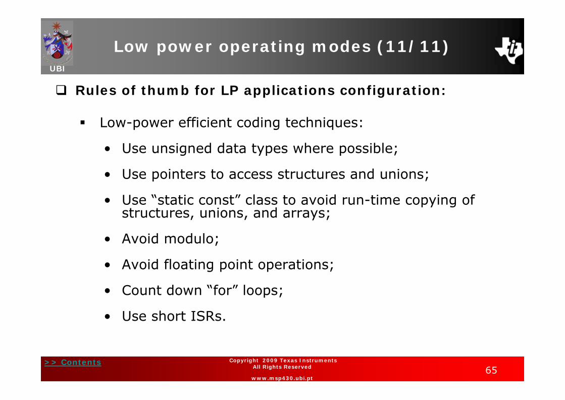
Low power operating modes (11/11)
Rules of thumb for LP applications configuration:
Low-power efficient coding techniques:
• Use unsigned data types where possible;
• Use pointers to access structures and unions;
• Use “static const” class to avoid run-time copying of structures, unions, and arrays;
• Avoid modulo;
• Avoid floating point operations;
• Count down “for” loops;
• Use short ISRs.

66
UBI
>> Contents Copyright 2009 Texas Instruments All Rights Reserved
www.msp430.ubi.pt
„C“ Code to Enter LPM
UBI
>> Contents
Chapter 7Timers
Description of clock signals
MSP430 Teaching Materials
Texas Instruments IncorporatedUniversity of Beira Interior (PT)
Pedro Dinis Gaspar, António Espírito Santo, Bruno Ribeiro, Humberto SantosUniversity of Beira Interior, Electromechanical Engineering Department
www.msp430.ubi.pt
Copyright 2008 Texas Instruments All Rights Reserved
www.msp430.ubi.pt

68
UBI
>> Contents Copyright 2009 Texas Instruments All Rights Reserved
www.msp430.ubi.pt
Contents
Introduction to timers
Clock signals available on the hardware development kits
Basic Timer1
Timer_A and Timer_B:Operating modesResetRegistersCap/Com blocksOutput modesTimer_A Cap/Com registersInterruptsTimer_B special featuresTimer_B register special bits
Quiz

69
UBI
>> Contents Copyright 2009 Texas Instruments All Rights Reserved
www.msp430.ubi.pt
Introduction (1/3)
Correct system timing is a fundamental requirement for the proper operation of a real-time application;
If the timing is incorrect, the input data may be processed after the output was updated;
The clock implementations vary among devices in the MSP430 family;
Each device provides different clock sources, controls and uses;
This chapter discusses the clock controls provided by the various MSP430 hardware platforms.

70
UBI
>> Contents Copyright 2009 Texas Instruments All Rights Reserved
www.msp430.ubi.pt
Introduction (2/3)
MSP430x4xx family:Two general purpose 16-bit or 8-bit counters and event timers: Timer_A, Timer_B;Basic Timer 1 (MSP430x4xx devices).
MSP430x2xx family:Also has Timer_A and Timer_B, as above;Basic Clock Module+.
The timers may be driven from an internal or external clock;
Timer_A and Timer_B also include multiple independent capture and compare blocks, with interrupt capabilities;
The capture and compare blocks are suited to applications such as:
Time events;Pulse Width Modulator (PWM).

71
UBI
>> Contents Copyright 2009 Texas Instruments All Rights Reserved
www.msp430.ubi.pt
Introduction (3/3)
The system timing is fundamental to nearly every embedded application;
The main applications of timers are to:
• Generate events of fixed time-period;
• Allow periodic wakeup from sleep of the device;
• Count transitional signal edges;
• Replacing delay loops with timer calls allows the CPU to sleep between operations, thus consuming less power.

72
UBI
>> Contents Copyright 2009 Texas Instruments All Rights Reserved
www.msp430.ubi.pt
Clock signals
The clock signals are controlled by two sets of registers (4xx family):
The first set of registers configures the low-frequency signals for use by peripheral modules:• Basic Timer Control Register (BTCTL);• Basic Timer Counter 1 (BTCNT1);• Basic Timer Counter 2 (BTCNT2).
The second set of registers is dedicated to the configuration of general-purpose system clocks:• System Clock Control (SCFQCTL);• System Clock Frequency Integrator 0 (SCFI0);• System Clock Frequency Integrator 1 (SCFI1);• Frequency Locked Loop control registers (FLL+CTL0,
FLL+CTL1).

73
UBI
>> Contents Copyright 2009 Texas Instruments All Rights Reserved
www.msp430.ubi.pt
Basic Timer1 (1/5)
The Basic Timer 1 module consists of two independent 8-bit timers:
Basic Timer 1 Counter 1 (BTCNT1);Basic Timer 1 Counter 2 (BTCNT2).
These can be used in cascade to form a 16-bit timer (software selectable by BTCTL register configuration);
The main characteristics of this module are:• Clock for a Liquid Crystal Display (LCD) module;• Suitable for a Real-Time Clock (RTC) implementation;• Basic interval timer;• Simple interrupt capability.

74
UBI
>> Contents Copyright 2009 Texas Instruments All Rights Reserved
www.msp430.ubi.pt
Basic Timer1 (2/5)
The control registers determine the operation of the Basic Timer 1 module:
• BTCNT1 (Read/write 8 bit register) - Generate the fLCD:– Clock source: ACLK;– Frame frequency selectable by software (BTFRFQx):
fLCD = ACLK/x.
• BTCNT2 (Read/write 8-bit register) - Programmable frequency divider to provide periodic CPU interrupts and/or a RTC system.– 3 possible clock sources:
» ACLK» SMCLK» ACLK/256 - cascaded with BTCNT1 (BTSSEL and
BTDIV bits in the BTCTL register);– Sources the Basic Timer1 interrupt, BTIFG, with
interval selected by BTIPx bits.

75
UBI
>> Contents Copyright 2009 Texas Instruments All Rights Reserved
www.msp430.ubi.pt
Basic Timer1 (3/5)
Block diagram:

76
UBI
>> Contents Copyright 2009 Texas Instruments All Rights Reserved
www.msp430.ubi.pt
Basic Timer1 (4/5)
Registers:BTCTL, Basic Timer 1 Control Register
BTIP0BTIP1BTIP2BTFRFQ0BTFRFQ1BTDIVBTHOLDBTSSEL
01234567
Basic Timer 1 interrupt interval: BTIP2 BTIP1 BTIP0 = 0 0 0 ⇒ fCLK2 / 2BTIP2 BTIP1 BTIP0 = 0 0 1 ⇒ fCLK2 / 4BTIP2 BTIP1 BTIP0 = 0 1 0 ⇒ fCLK2 / 8BTIP2 BTIP1 BTIP0 = 0 1 1 ⇒ fCLK2 / 16BTIP2 BTIP1 BTIP0 = 1 0 0 ⇒ fCLK2 / 32BTIP2 BTIP1 BTIP0 = 1 0 1 ⇒ fCLK2 / 64BTIP2 BTIP1 BTIP0 = 1 1 0 ⇒ fCLK2 / 128BTIP2 BTIP1 BTIP0 = 1 1 1 ⇒ fCLK2 / 256
BTIPX2-0
LCD frame frequency: BTFRFQ1 BTFRFQ0 = 0 0 ⇒ fACLK/32BTFRFQ1 BTFRFQ0 = 0 1 ⇒ fACLK/64BTFRFQ1 BTFRFQ0 = 1 0 ⇒ fACLK/128BTFRFQ1 BTFRFQ0 = 1 1 ⇒ fACLK/256
BTFRFFQx4-3
Basic Timer 1 clock divider: BTSSEL BTDIV = 0 0 ⇒ ACLKBTSSEL BTDIV = 0 1 ⇒ ACLK/256BTSSEL BTDIV = 1 0 ⇒ SMCLKBTSSEL BTDIV = 1 1 ⇒ ACLK/256
BTDIV5
Basic Timer 1 hold: BTHOLD = 0 ⇒ BTCNT1 and BTCNT2 activeBTHOLD = 1 ⇒ BTCNT1 hold, if BTDIV = 1BTHOLD = 1 ⇒ BTCNT1 and BTCNT2 hold
BTHOLD6
BTCNT2 clock select (together with the BTDIV bit)BTSSEL7
DescriptionBit

77
UBI
>> Contents Copyright 2009 Texas Instruments All Rights Reserved
www.msp430.ubi.pt
Basic Timer1 (5/5)
Registers:IE2, Interrupt Enable Register 2
IFG2, Interrupt Flag Register 2
BTIE
07
Basic Timer 1 interrupt enable when BTIE = 1BTIE7
DescriptionBit
BTIFG
07
Basic Timer 1 interrupt flag BTIFG = 1 when interrupt pendingBTIFG7
DescriptionBit

78
UBI
>> Contents Copyright 2009 Texas Instruments All Rights Reserved
www.msp430.ubi.pt
Timer_A and Timer_B Introduction (1/6)
Timer A and B are two general-purpose 16-bit counter/event timers;
There are slight differences between the two timers;
Features common to both timers include:Asynchronous 16-bit timer/counter with four operating modes:• Timer_A length: 16 bits;• Timer_B length: programmable: 8, 10, 12, or 16 bits.• Timer/counter register, TAR (Timer_A) or TBR
(Timer_B) -from now on described as TxR- increments or decrements (depending on mode of operation) with each rising edge of the clock signal;
• The timer can generate an interrupt when it overflows;• Wide interrupt interval range: 1/MCLK to 32 seconds.

79
UBI
>> Contents Copyright 2009 Texas Instruments All Rights Reserved
www.msp430.ubi.pt
Timer_A and Timer_B Introduction (2/6)
Choice of selectable and configurable clock source:• ACLK;• SMCLK;• External - via TACLK or INCLK (TASSELx bits);• The selected clock source may additionally be divided
by 2, 4, or 8 (IDx bits configuration).
Configurable capture/compare registers:• Timer_A has 3 or 5 capture/compare registers;• Timer_B has 3 or 7 capture/compare registers;• Timer_B capture/compare registers can be grouped.

80
UBI
>> Contents Copyright 2009 Texas Instruments All Rights Reserved
www.msp430.ubi.pt
Timer_A and Timer_B Introduction (3/6)
Configurable outputs and internal connections to several other modules:• Faster response; • No cycles are wasted while the Interrupt Service
Routine ( ISR) loads/executes;• Avoids CPU wakeup;• Saves power.
• Outputs capability: Pulse Width Modulation (PWM);
• Comparator_A;
• Direct Memory Access (DMA);
• Digital-to-Analogue Converter (DAC12).

81
UBI
>> Contents Copyright 2009 Texas Instruments All Rights Reserved
www.msp430.ubi.pt
Timer_A and Timer_B Introduction (4/6)
Asynchronous input and output latching:• Timer_A Capture/Compare (Cap/Com) registers are not
buffered, being updated immediately when written to;• Timer_B Cap/Com registers are double-buffered with
synchronized loading.
Interrupt vector register for fast decoding of all Timer_A and Timer_B interrupts:• TACCR0 (or TBCCR0) interrupt vector for TACCR0 (or
TBCCCR0) CCIFG;• TAIV (or TBIV) interrupt vector for the remaining CCIFG
flags and TAIFG (or TBIFG).

82
UBI
>> Contents Copyright 2009 Texas Instruments All Rights Reserved
www.msp430.ubi.pt
Timer_A and Timer_B Introduction (5/6)
Block diagram (Timer_A):

83
UBI
>> Contents Copyright 2009 Texas Instruments All Rights Reserved
www.msp430.ubi.pt
Timer_A and Timer_B Introduction (6/6)
Timers have four modes of operation:• MCx bits (Timer_A or Timer_B Control Register)
Up/down counting mode (from 0x0000 to the value in the TACCR0 or TBCCR0 register and back down to zero)
Up/down1 1Continuous counting mode (from 0x0000 to 0xFFFF)Continuous1 0
Up counting mode (from 0x0000 to the value in the TACCR0 or TBCCR0 register)
Up0 1The timer is haltedStop0 0DescriptionModeMCx

84
UBI
>> Contents Copyright 2009 Texas Instruments All Rights Reserved
www.msp430.ubi.pt
Timer_A and Timer_B operating modes (1/3)
Up mode:TxR counts up till it reaches the value in the TxCCR0 register;TxR->TxCCR0: TACCR0 interrupt flag, CCIFG, is set;TxR=TxCCR0: EQU0 = 1 (restarts counting in TxR);TxCCR0->0: TxIFG interrupt flag is set:• Interrupt period:
tINT = 1/[fCLK/Prescaler/(TxCCR0+1)].

85
UBI
>> Contents Copyright 2009 Texas Instruments All Rights Reserved
www.msp430.ubi.pt
Timer_A and Timer_B operating modes (2/3)
Continuous mode:TxR counts up till it reaches 0xFFFF (65536 counts);TxR=0xFFFF: TxR counting from zero (next clock pulse);0xFFFF->0: TxIFG interrupt flag is set:• Interrupt period: tINT = 1/[fCLK/Prescaler/65536];
(Correct only for TAR; for TBR 4 different end values. See User’s Guide for additional details).

86
UBI
>> Contents Copyright 2009 Texas Instruments All Rights Reserved
www.msp430.ubi.pt
Timer_A and Timer_B operating modes (3/3)
Up/down mode:TxR counts up till it reaches the value in the TxCCR0 register;TxCCR0-1 -> TxCCR0: Interrupt flag, CCIFG, is set;TxR=TxCCR0: Counting is inverted;0x0001->0x0000: Interrupt flag TxIFG is set:• Interrupt period: tINT = 1/[fCLK/Prescaler/(TxCCR0×2];

87
UBI
>> Contents Copyright 2009 Texas Instruments All Rights Reserved
www.msp430.ubi.pt
Timer_A and Timer_B reset
The timers can be reset by the following actions:Writing 0 in the TxR register;
Writing 0 in the TxCCR0 register, provided that the timer is not in continuous mode;
Setting the TxCLR bit in the Timer Control Register (TxCTL).

88
UBI
>> Contents Copyright 2009 Texas Instruments All Rights Reserved
www.msp430.ubi.pt
Timer_A and Timer_B registers
TACTL, Timer_A Control Register
TASSEL0TASSEL1Unused
891015
TAIFGTAIETACLRUnusedMC0MC1ID0ID1
01234567
Timer_A interrupt pending when TAIFG = 1TAIFG0
Timer_A interrupt enable when TAIE = 1TAIE1
Timer_A clear when TACLR = 1TACLR2
Clock timer operating mode: MC1 MC0 = 0 0 ⇒ Stop modeMC1 MC0 = 0 1 ⇒ Up modeMC1 MC0 = 1 0 ⇒ Continuous modeMC1 MC0 = 1 1 ⇒ Up/down mode
MCx5-4
Clock signal divider: ID1 ID0 = 0 0⇒ / 1ID1 ID0 = 0 1⇒ / 2ID1 ID0 = 1 0⇒ / 4ID1 ID0 = 1 1⇒ / 8
IDx7-6
Timer_A clock source: TASSEL1 TASSEL0 = 0 0 ⇒ TACLKTASSEL1 TASSEL0 = 0 1 ⇒ ACLKTASSEL1 TASSEL0 = 1 0 ⇒ SMCLKTASSEL1 TASSEL0 = 1 1 ⇒ INCLK
TASSELx9-8
DescriptionBit

89
UBI
>> Contents Copyright 2009 Texas Instruments All Rights Reserved
www.msp430.ubi.pt
Timer_A and Timer_B Cap/Com blocks (1/5)
Timer_A (and Timer_B) contain independent capture and compare blocks, TACCRx (or TBCCRx);
These blocks may be used to capture timer register contents, as they are at the time of an event, or to generate an event when the timer register contents correspond to the capture/compare register contents, e.g. to generate time intervals;
The setting of capture/compare is selected by the modebit CAP in the individual Capture/Compare Controlregisters, TACCTLx (or TBCCTLx)

90
UBI
>> Contents Copyright 2009 Texas Instruments All Rights Reserved
www.msp430.ubi.pt
Timer_A and Timer_B Cap/Com blocks (2/5)
Capture mode:Used to measure the period of time events with minimal CPU intervention.
Procedure:• Set the CAP bit to select capture mode;
• Set the SCS bit to synchronize the capture with the next timer clock (recommended to avoid race conditions);
• The input signal is sampled by the CCIxA (or CCIxB) input, selected by the CCISx bits in the Capture/Compare Control Register, TACCTLx (or TBCCTLx);

91
UBI
>> Contents Copyright 2009 Texas Instruments All Rights Reserved
www.msp430.ubi.pt
Timer_A and Timer_B Cap/Com blocks (3/5)
• The capture edge of the input signal (rising, falling, or both) is selected by the CMx bits;
• When a valid edge is detected on the selected input line, the value in the Timer register is latched into the TACCRx (or TBCCRx) register, providing a time mark for the event;
• The interrupt flag CCIFG is set;
• The bit COV (=1) controls an overflow event when a second capture is performed, before the value from the first capture is read.

92
UBI
>> Contents Copyright 2009 Texas Instruments All Rights Reserved
www.msp430.ubi.pt
Timer_A and Timer_B Cap/Com blocks (4/5)
Compare mode:Used for pulse generation or generation of interrupts at specific time intervals (PWM output signals).
Procedure:• Reset the CAP bit to select compare mode;
• TxR counts up to the value programmed in the TxCCRx register;
• When the timer value is equal to the value in the TxCCRx register, an interrupt is generated:– Interrupt flag CCIFG is set;– Internal signal EQUx = 1 (where x is the number of
the CCR channel).

93
UBI
>> Contents Copyright 2009 Texas Instruments All Rights Reserved
www.msp430.ubi.pt
Timer_A and Timer_B Cap/Com blocks (5/5)
• EQUx affects the output compare signal OUTx according to the output mode (defined by the OUTMODx bits in the TxCCTL;
• The input signal CCI is latched into SCCI.
Output operating modes uses:Modes 2, 3, 6 and 7: PWM output signals;Mode 3: active PWM signal at low state;Mode 7: active PWM signal at high state;Modes 2 and 6: complementary PWM signals;Modes 1 and 5: single event generation;Mode 4: signal with 1/2 frequency of the timer signal.

94
UBI
>> Contents Copyright 2009 Texas Instruments All Rights Reserved
www.msp430.ubi.pt
Timer_A and Timer_B Output modes (1/2)
Output operating modes (OUTMODx bits):
OUTx = 0 ⇒ timer = TxCCRxOUTx = 1 ⇒ timer = TxCCR0
Reset/Set1 1 1
OUTx = toggle ⇒ timer = TxCCRxOUTx = 1 ⇒ timer = TxCCR0
Toggle/Set1 1 0
OUTx = 0 ⇒ timer = TxCCRxOUTx = 1 ⇒ another output mode is selected and affects the output
Reset1 0 1
OUTx = toggle ⇒ timer = TxCCRxThe output period is double the timer period
Toggle1 0 0
OUTx = 1 ⇒ timer = TxCCRxOUTx = 0 ⇒ timer = TxCCR0
Set/Reset0 1 1
OUTx = toggle ⇒ timer = TxCCRxOUTx = 0 ⇒ timer = TxCCR0
Toggle/Reset0 1 0
OUTx = 1 ⇒ timer = TxCCRxOUTx = 0 ⇒ timer = 0 or until another output mode is selected and
affects the output
Set0 0 1
The output signal OUTx is defined by the bit OUTxOutput0 0 0
DescriptionModeOUTMODx

95
UBI
>> Contents Copyright 2009 Texas Instruments All Rights Reserved
www.msp430.ubi.pt
Timer_A and Timer_B Output modes (2/2)
Output examples:

96
UBI
>> Contents Copyright 2009 Texas Instruments All Rights Reserved
www.msp430.ubi.pt
Timer_A Cap/Com registers (1/2)
TACCTLx, Timer_A Cap/Com Control Register
CAPUnusedSCCISCSCCIS0CCIS1CM0CM1
89101112131415
Mode: Capture mode ⇒ CAP = 1Compare mode ⇒ CAP = 0
CAP8
Synchronized capture/compare inputSCCI10
Synchronize capture input signal with timer clock:SCS = 0 ⇒ Asynchronous captureSCS = 1 ⇒ Synchronous capture
SCS11
Capture/compare input select: CCIS1 CCIS0 = 0 0 ⇒ CCIxACCIS1 CCIS0 = 0 1 ⇒ CCIxBCCIS1 CCIS0 = 1 0 ⇒ GNDCCIS1 CCIS0 = 1 1 ⇒ Vcc
CCISx13-12
Capture mode: CM1 CM0 = 0 0 ⇒ No captureCM1 CM0 = 0 1 ⇒ Capture on rising edgeCM1 CM0 = 1 0 ⇒ Capture on falling edgeCM1 CM0 = 1 1 ⇒ Capture on both edges
CMx15-14
DescriptionBit

97
UBI
>> Contents Copyright 2009 Texas Instruments All Rights Reserved
www.msp430.ubi.pt
Timer_A Cap/Com registers (2/2)
TACCTLx, Timer_A Cap/Com Control Register
CCIFGCOVOUTCCICCIEOUTMOD0OUTMOD1OUTMOD2
01234567
Capture/compare interrupt flag CCIFG = 1 when interrupt pendingCCIFG0
Capture overflow when COV = 1COV1
Output stateOUT2
Capture/compare inputCCI3
Capture/compare interrupt enable when CCIE = 1.CCIE4
Output mode: OUTMOD2 OUTMOD1 OUTMOD0 = 0 0 0 ⇒ bit OUTOUTMOD2 OUTMOD1 OUTMOD0 = 0 0 1 ⇒ SetOUTMOD2 OUTMOD1 OUTMOD0 = 0 1 0 ⇒ Toggle/ResetOUTMOD2 OUTMOD1 OUTMOD0 = 0 1 1 ⇒ Set / ResetOUTMOD2 OUTMOD1 OUTMOD0 = 1 0 0 ⇒ ToggleOUTMOD2 OUTMOD1 OUTMOD0 = 1 0 1 ⇒ ResetOUTMOD2 OUTMOD1 OUTMOD0 = 1 1 0 ⇒ Toggle / SetOUTMOD2 OUTMOD1 OUTMOD0 = 1 1 1 ⇒ Reset / Set
OUTMODx7-5
DescriptionBit

98
UBI
>> Contents Copyright 2009 Texas Instruments All Rights Reserved
www.msp430.ubi.pt
Timer_A and Timer_B Interrupts (1/3)
Interrupt characteristics:
Capture mode:• Any CCIFG flag is set when a timer value is captured in
the associated TxCCRx register.
Compare mode:• Any CCIFG flag is set if TxR counts up to the TxCCRx
value.
• Software may also set or clear a CCIFG flag;
• All CCIFG flags request an interrupt when their corresponding CCIE bit and GIE bit are set.

99
UBI
>> Contents Copyright 2009 Texas Instruments All Rights Reserved
www.msp430.ubi.pt
Timer_A and Timer_B Interrupts (2/3)
Interrupt vectors associated with Timer_A:
TACCR0 interrupt vector for TACCR0 CCIFG:• TACCR0 CCIFG flag has the highest priority Timer_A
interrupt;
• The TACCR0 CCIFG flag is automatically reset when the TACCR0 interrupt request is serviced.

100
UBI
>> Contents Copyright 2009 Texas Instruments All Rights Reserved
www.msp430.ubi.pt
Timer_A and Timer_B Interrupts (3/3)
Interrupt vectors associated with Timer_A (continued):
TAIV interrupt vector for TACCR1 CCIFG to TACCR4 CCIFG and TAIFG:• Flags are given priority and combined to source a single
interrupt vector (decreasing priority);
• TAIV determines which flag requests the interrupt;
• Disabling interrupts do not affect the value in TAIV;
• Any access (read/write) of TAIV automatically resets the highest pending interrupt flag;
• If another interrupt flag is set, another interrupt is immediately generated after servicing the initial interrupt.
101
UBI
>> Contents Copyright 2009 Texas Instruments All Rights Reserved
www.msp430.ubi.pt
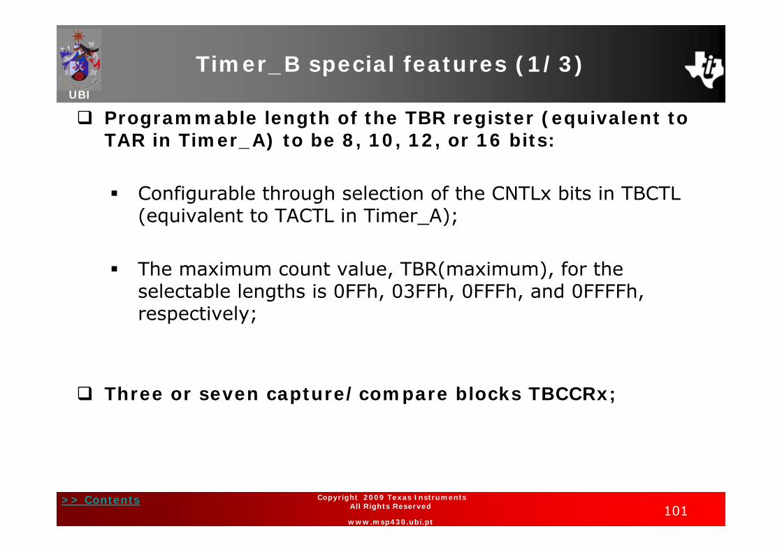
Timer_B special features (1/3)
Programmable length of the TBR register (equivalent to TAR in Timer_A) to be 8, 10, 12, or 16 bits:
Configurable through selection of the CNTLx bits in TBCTL (equivalent to TACTL in Timer_A);
The maximum count value, TBR(maximum), for the selectable lengths is 0FFh, 03FFh, 0FFFh, and 0FFFFh, respectively;
Three or seven capture/compare blocks TBCCRx;

102
UBI
>> Contents Copyright 2009 Texas Instruments All Rights Reserved
www.msp430.ubi.pt
Timer_B special features (2/3)
Double-buffered compare latches with synchronized loading:
In Timer_A, the signal generation in compare mode may cause noise during compare period updates because the TACRRx value is used directly to compare with the timer value;
To avoid this condition, the compare latches TBCLx, buffered by TBCCRx, holds the data for the comparison to the timer value in compare mode;
The CLLDx bits at the TBCCTLx register configure the timing of the transfer from TBCCRx to TBCLx.

103
UBI
>> Contents Copyright 2009 Texas Instruments All Rights Reserved
www.msp430.ubi.pt
Timer_B special features (3/3)
Grouping channels capability:Multiple compare latches may be grouped together for simultaneous updates of the TBCLGRPx bits;
Two conditions are required:• All TBCCRx registers must be updated;• The load event controlled by the CLLDx bits must occur.
All outputs can be put into a high-impedance state:TBOUTH = 1 puts Timer_B outputs into a high-impedance state, allowing higher security and lower delay time responding to failures.
The SCCI bit function is not implemented.

104
UBI
>> Contents Copyright 2009 Texas Instruments All Rights Reserved
www.msp430.ubi.pt
Timer_B registers special bits (1/2)
TBCTL, Timer_B Control Register
TBSSEL0TBSSEL1UnusedCNTL0CNTL1TBCLGRP0TBCLGRP1Unused
89101112131415
TBIFGTBIETBCLRUnusedMC0MC1ID0ID1
01234567
Counter Length: CNTL1 CNTL0 = 0 0 ⇒ 16-bit, TBR(max) = 0FFFFhCNTL1 CNTL0 = 0 1 ⇒ 12-bit, TBR(max) = 0FFFhCNTL1 CNTL0 = 1 0 ⇒ 10-bit, TBR(max) = 03FFhCNTL1 CNTL0 = 1 1 ⇒ 8-bit, TBR(max) = 0FFh
CNTLx12-11
TBCLx group:TBCLGRP1 TBCLGRP0 = 0 0 ⇒ Each TBCLx latch loads independentlyTBCLGRP1 TBCLGRP0 = 0 1 ⇒ TBCL1+TBCL2 (update control: TBCCR1 CLLDx)
⇒ TBCL3+TBCL4 (update control: TBCCR3 CLLDx)⇒ TBCL5+TBCL6 (update control: TBCCR5 CLLDx)⇒ TBCL0 independent
TBCLGRP1 TBCLGRP0 = 1 0 ⇒ TBCL1+TBCL2+TBCL3 (update control: TBCCR1 CLLDx)⇒ TBCL4+TBCL5+TBCL6 (update control: TBCCR4 CLLDx)⇒ TBCL0 independent
TBCLGRP1 TBCLGRP0 = 1 1 ⇒ TBCL0+TBCL1+TBCL2+TBCL3+TBCL4+TBCL5+TBCL6(update control: TBCCR1 CLLDx)
TBCLGRPx14-13
DescriptionBit

105
UBI
>> Contents Copyright 2009 Texas Instruments All Rights Reserved
www.msp430.ubi.pt
Timer_B registers special bits (2/2)
TBCCTLx, Timer_B Capture/Compare Control Register
CAPCLLD0CLLD1SCSCCIS0CCIS1CM0CM1
89101112131415
CCIFGCOVOUTCCICCIEOUTMOD0OUTMOD1OUTMOD2
01234567
Compare latch load:CLLD1 CLLD0 = 0 0 ⇒ TBCLx loads on write to TBCCRxCLLD1 CLLD0 = 0 1 ⇒ TBCLx loads when TBR counts to 0CLLD1 CLLD0 = 1 0 ⇒ TBCLx loads when TBR counts:
- to 0 (up/continuous mode);- to TBCL0 or to 0 (up/down
mode)CLLD1 CLLD0 = 1 1 ⇒ TBCLx loads when TBR counts:
- to TBCLx
CLLDx10-9
DescriptionBit


![[MSP430] ADC10](https://img.pdfslide.net/doc/110x75/55cf97c5550346d033938430/msp430-adc10-5654b9a37ede3.jpg)


![[MSP430] GPIO](https://img.pdfslide.net/doc/110x75/55cf9df0550346d033aff200/msp430-gpio.jpg)