Embed Size (px)
Citation preview
Product
Folder
Sample &Buy
Technical
Documents
Tools &
Software
Support &Community
An IMPORTANT NOTICE at the end of this data sheet addresses availability, warranty, changes, use in safety-critical applications,intellectual property matters and other important disclaimers. PRODUCTION DATA.
MSP430F2619S-HTSLAS697E –MARCH 2010–REVISED NOVEMBER 2016
MSP430F2619S-HT Mixed-Signal Microcontroller
1 Device Overview
1
1.1 Features1
• Low-Supply Voltage Range 1.8 V to 3.6 V• Ultra-Low Power Consumption
– Active Mode: 365 μA at 1 MHz, 2.2 V– Standby Mode (VLO): 0.5 μA– Off Mode (RAM Retention): 0.1 μA
• Wake-Up From Standby Mode in Less than 1 μs• 16-Bit RISC Architecture, 62.5-ns Instruction Cycle
Time• Three-Channel Internal DMA• 12-Bit Analog-to-Digital (A/D) Converter With
Internal Reference, Sample-and-Hold, andAutoscan Feature
• Dual 12-Bit Digital-to-Analog (D/A) Converters WithSynchronization
• 16-Bit Timer_A With Three Capture/CompareRegisters
• 16-Bit Timer_B With Seven Capture/Compare-With-Shadow Registers
• On-Chip Comparator
• Four Universal Serial Communication Interfaces(USCIs)– USCI_A0 and USCI_A1
– Enhanced UART Supporting Auto-Baud-RateDetection (LIN)
– IrDA Encoder and Decoder– Synchronous SPI
– USCI_B0 and USCI_B1– I2C– Synchronous SPI
• Supply Voltage Supervisor/Monitor WithProgrammable Level Detection
• Brownout Detector• Bootstrap Loader• Serial Onboard Programming, No External
Programming Voltage Needed ProgrammableCode Protection by Security Fuse
• MSP430F2619S 120KB + 256B Flash Memory,4KB RAM
• Available in 64-Pin QFP Package or 64-Pin and80-Pin KGD Options
• For Complete Module Descriptions, Refer toMSP430x2xx Family User's Guide (SLAU144).
1.2 Applications• Supports Extreme Temperature Applications:
– Controlled Baseline– One Assembly/Test Site– One Fabrication Site– Extended Product Life Cycle– Extended Product-Change Notification– Product Traceability
• This device is qualified for 1000 hours ofcontinuous operation at maximum ratedtemperature.
• TI high-temperature products use highly-optimizedsilicon (die) solutions with design and processenhancements to maximize performance overextended temperatures.
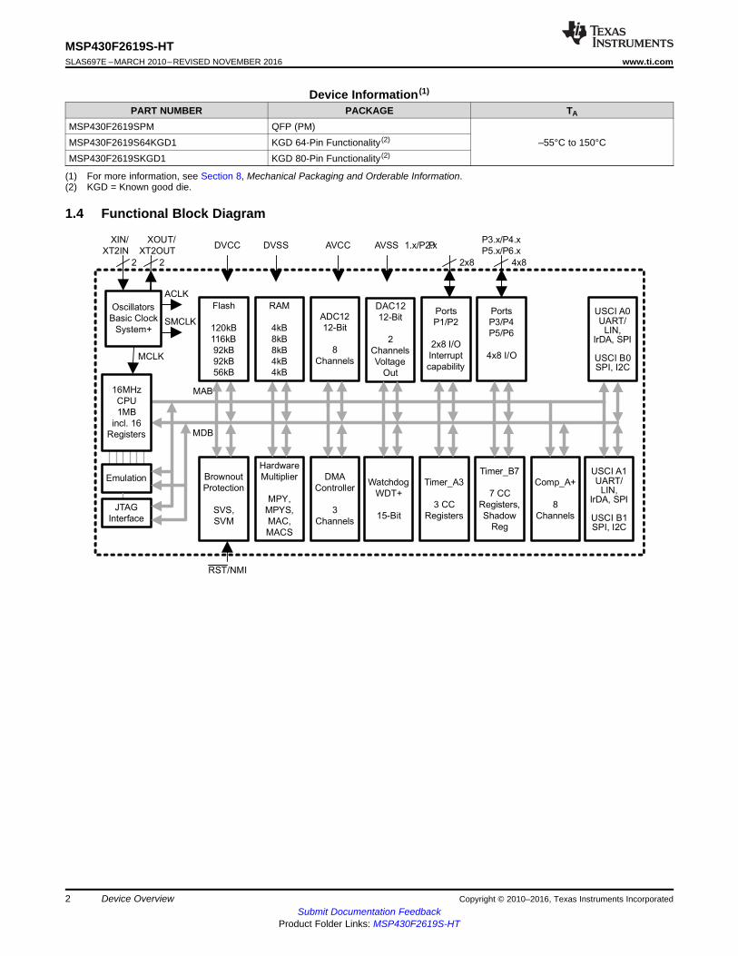
1.3 DescriptionThe MSP430F2619S ultra-low-power microcontroller features different sets of peripherals targeted forvarious applications. The architecture, combined with five low-power modes, is optimized to achieveextended battery life in portable measurement applications. The device features a powerful 16-bit RISCCPU, 16-bit registers, and constant generators that attribute to maximum code efficiency. The digitallycontrolled oscillator (DCO) allows wake-up from low-power modes to active mode in less than 1 μs.
The MSP430F2619S is a microcontroller configuration with two built-in 16-bit timers, a fast 12-bit A/Dconverter, a comparator, dual 12-bit D/A converters, four universal serial communication interface (USCI)modules, DMA, and up to 64 I/O pins.
Typical applications include sensor systems that capture analog signals, convert them to digital values,and then process the data for display or for transmission to a host system. Stand-alone RF sensor frontend is another area of application.
USCI A0UART/
LIN,IrDA, SPI
USCI B0SPI, I2C
Oscillators
Basic Clock
System+
Brownout
Protection
SVS,
SVM
RST/NMI
DVCC DVSS
MCLK
Watchdog
WDT+
15-Bit
Timer_A3
3 CC
Registers
16MHz
CPU
1MB
incl. 16
Registers
Emulation
JTAG
Interface
Ports
P1/P2
2x8 I/O
Interrupt
capability
Comp_A+
8
Channels
Hardware
Multiplier
MPY,
MPYS,
MAC,
MACS
Timer_B7
7 CC
Registers,
Shadow
Reg
ADC12
12-Bit
8
Channels
Ports
P3/P4
P5/P6
4x8 I/O
AVCC AVSS P1.x/P2.x
2x8
P3.x/P4.x
P5.x/P6.x
4x8
SMCLK
ACLK
MDB
MAB
DAC12
12-Bit
2
Channels
Voltage
Out
DMA
Controller
3
Channels
XIN/
XT2IN
22
XOUT/
XT2OUT
RAM
4kB
8kB
8kB
4kB
4kB
Flash
120kB
116kB
92kB
92kB
56kB
USCI A1UART/
LIN,IrDA, SPI
USCI B1SPI, I2C
2
MSP430F2619S-HTSLAS697E –MARCH 2010–REVISED NOVEMBER 2016 www.ti.com
Submit Documentation FeedbackProduct Folder Links: MSP430F2619S-HT
Device Overview Copyright © 2010–2016, Texas Instruments Incorporated
(1) For more information, see Section 8, Mechanical Packaging and Orderable Information.(2) KGD = Known good die.
Device Information (1)
PART NUMBER PACKAGE TA
MSP430F2619SPM QFP (PM)–55°C to 150°CMSP430F2619S64KGD1 KGD 64-Pin Functionality (2)
MSP430F2619SKGD1 KGD 80-Pin Functionality (2)
1.4 Functional Block Diagram
3
MSP430F2619S-HTwww.ti.com SLAS697E –MARCH 2010–REVISED NOVEMBER 2016
Submit Documentation FeedbackProduct Folder Links: MSP430F2619S-HT
Table of ContentsCopyright © 2010–2016, Texas Instruments Incorporated
Table of Contents1 Device Overview ......................................... 1
1.1 Features .............................................. 11.2 Applications........................................... 11.3 Description............................................ 11.4 Functional Block Diagram ............................ 2
2 Revision History ......................................... 53 Terminal Configurations and Functions ............ 6
3.1 Pin Diagram .......................................... 63.2 Pin Attributes ......................................... 73.3 Bare Die Information ................................ 10
4 Specifications ........................................... 154.1 Absolute Maximum Ratings ........................ 154.2 ESD Ratings ........................................ 154.3 Recommended Operating Conditions .............. 154.4 Thermal Information................................. 174.5 Active-Mode Supply Current Into AVCC Excluding
External Current –Electrical Characteristics ........................... 17
4.6 Typical Characteristics – Active-Mode SupplyCurrent (Into DVCC + AVCC)......................... 18
4.7 Active-Mode Current vs DCO Frequency ........... 194.8 Low-Power-Mode Supply Currents Into AVCC
Excluding External Current – ElectricalCharacteristics ...................................... 20
4.9 Typical Characteristics – LPM4 Current ............ 214.10 Schmitt-Trigger Inputs (Ports P1 Through P6, and
RST/NMI, JTAG, XIN, and XT2IN) – ElectricalCharacteristics ...................................... 22
4.11 Inputs (Ports P1 and P2) – ElectricalCharacteristics....................................... 22
4.12 Leakage Current (Ports P1 Through P6) – ElectricalCharacteristics....................................... 22
4.13 Standard Inputs - RST/NMI – ElectricalCharacteristics....................................... 22
4.14 Outputs (Ports P1 Through P6) – ElectricalCharacteristics....................................... 23
4.15 Output Frequency (Ports P1 Through P6) –Electrical Characteristics ............................ 23
4.16 Typical Characteristics – Outputs ................... 244.17 POR/Brownout Reset (BOR) – Electrical
Characteristics ...................................... 254.18 Typical Characteristics - POR/Brownout Reset
(BOR)................................................ 264.19 SVS (Supply Voltage Supervisor/Monitor) -
Electrical Characteristics ............................ 274.20 Typical Characteristics - SVS ....................... 284.21 Main DCO Characteristics .......................... 294.22 DCO Frequency – Electrical Characteristics........ 294.23 Calibrated DCO Frequencies (Tolerance at
Calibration) – Electrical Characteristics ............. 304.24 Calibrated DCO Frequencies (Tolerance Over
Temperature) – Electrical Characteristics........... 314.25 Calibrated DCO Frequencies (Tolerance Over
Supply Voltage VCC) – Electrical Characteristics ... 324.26 Calibrated DCO Frequencies (Overall Tolerance) –
Electrical Characteristics ............................ 32
4.27 Typical Characteristics – Calibrated DCOFrequency ........................................... 33
4.28 Wake-Up From Low-Power Modes (LPM3/4) –Electrical Characteristics ........................... 34
4.29 Typical Characteristics – DCO Clock Wake-Up TimeFrom LPM3/4........................................ 34
4.30 DCO With External Resistor ROSC – ElectricalCharacteristics ...................................... 34
4.31 Typical Characteristics - DCO With ExternalResistor ROSC ...................................... 35
4.32 Crystal Oscillator (LFXT1) Low-Frequency Modes –Electrical Characteristics ........................... 36
4.33 Internal Very-Low-Power, Low-Frequency Oscillator(VLO) – Electrical Characteristics................... 36
4.34 Crystal Oscillator (LFXT1) High Frequency Modes –Electrical Characteristics ........................... 37
4.35 Typical Characteristics – LFXT1 Oscillator in HFMode (XTS = 1) ..................................... 38
4.36 Crystal Oscillator (XT2) – Electrical Characteristics...................................................... 39
4.37 Typical Characteristics – XT2 Oscillator ............ 404.38 Timer_A – Electrical Characteristics ................ 404.39 Timer_B – Electrical Characteristics ................ 404.40 USCI (UART Mode) – Electrical Characteristics .... 404.41 USCI (SPI Master Mode) – Electrical
Characteristics....................................... 414.42 USCI (SPI Slave Mode) – Electrical Characteristics 424.43 USCI (I2C Mode) – Electrical Characteristics....... 454.44 Comparator_A+ – Electrical Characteristics ....... 464.45 Typical Characteristics – Comparator A+ ........... 484.46 12-Bit ADC Power-Supply and Input Range
Conditions – Electrical Characteristics ............. 494.47 12-Bit ADC External Reference – Electrical
Characteristics....................................... 504.48 12-Bit ADC Built-In Reference – Electrical
Characteristics....................................... 514.49 Typical Characteristics – ADC12.................... 514.50 12-Bit ADC Timing Parameters – Electrical
Characteristics....................................... 534.51 12-Bit ADC Linearity Parameters – Electrical
Characteristics ...................................... 534.52 12-Bit ADC Temperature Sensor and Built-In VMID –
Electrical Characteristics ............................ 544.53 12-Bit DAC Supply Specifications – Electrical
Characteristics ...................................... 544.54 12-Bit DAC Linearity Parameters – Electrical
Characteristics ...................................... 554.55 Typical Characteristics - 12-Bit DAC Linearity
Specifications........................................ 564.56 12-Bit DAC Output Specifications – Electrical
Characteristics ...................................... 574.57 12-Bit DAC Reference Input Specifications –
Electrical Characteristics ............................ 584.58 12-Bit DAC Dynamic Specifications, VREF = VCC,
DAC12IR = 1 – Electrical Characteristics ........... 594.59 Flash Memory – Electrical Characteristics .......... 604.60 RAM – Electrical Characteristics.................... 614.61 JTAG and Spy-Bi-Wire Interface – Electrical
4
MSP430F2619S-HTSLAS697E –MARCH 2010–REVISED NOVEMBER 2016 www.ti.com
Submit Documentation FeedbackProduct Folder Links: MSP430F2619S-HT
Table of Contents Copyright © 2010–2016, Texas Instruments Incorporated
Characteristics....................................... 614.62 JTAG Fuse – Electrical Characteristics ............. 62
5 Detailed Description ................................... 635.1 CPU ................................................. 635.2 Instruction Set....................................... 635.3 Operating Modes.................................... 645.4 Interrupt Vector Addresses.......................... 655.5 Special Function Registers.......................... 665.6 Memory Organization ............................... 685.7 Bootstrap Loader (BSL) ............................. 685.8 Flash Memory ....................................... 685.9 Peripherals .......................................... 695.10 DMA Controller...................................... 695.11 Oscillator and System Clock ........................ 695.12 Brownout, Supply Voltage Supervisor (SVS) ....... 705.13 Digital I/O............................................ 705.14 WDT+ Watchdog Timer ............................. 705.15 Hardware Multiplier ................................. 705.16 USCI................................................. 705.17 Timer_A3 ............................................ 715.18 Timer_B7 ............................................ 725.19 Comparator_A+ ..................................... 735.20 ADC12............................................... 735.21 DAC12............................................... 735.22 Peripheral File Map ................................. 73
6 Applications, Implementation, and Layout........ 786.1 P1.0 to P1.7, Input/Output With Schmitt Trigger.... 786.2 P2.0 to P2.4, P2.6, and P2.7, Input/Output With
Schmitt Trigger ...................................... 796.3 P2.5, Input/Output With Schmitt Trigger and
External ROSC for DCO.............................. 81
6.4 Port P3 Pin Schematic: P3.0 to P3.7, Input/OutputWith Schmitt Trigger ................................ 82
6.5 Port P4 Pin Schematic: P4.0 to P4.7, Input/OutputWith Schmitt Trigger ................................ 83
6.6 Port P5 Pin Schematic: P5.0 to P5.7, Input/OutputWith Schmitt Trigger ................................ 84
6.7 Port P6 Pin Schematic: P6.0 to P6.4, Input/OutputWith Schmitt Trigger ................................ 85
6.8 Port P6 Pin Schematic: P6.5 and P6.6, Input/OutputWith Schmitt Trigger ................................ 86
6.9 Port P6 Pin Schematic: P6.7, Input/Output WithSchmitt Trigger ...................................... 87
6.10 Port P7 Pin Schematic: P7.0 to P7.7, Input/OutputWith Schmitt Trigger ................................ 88
6.11 Port P8 Pin Schematic: P8.0 to P8.5, Input/OutputWith Schmitt Trigger ................................ 89
6.12 Port P8 Pin Schematic: P8.6, Input/Output WithSchmitt Trigger ...................................... 90
6.13 Port P8 Pin Schematic: P8.7, Input/Output WithSchmitt Trigger ...................................... 91
6.14 JTAG Pins: TMS, TCK, TDI/TCLK, TDO/TDI,Input/Output With Schmitt Trigger .................. 92
6.15 JTAG Fuse Check Mode............................ 937 Device and Documentation Support ............... 94
7.1 Development Tool Support.......................... 947.2 Receiving Notification of Documentation Updates .. 947.3 Community Resources .............................. 947.4 Trademarks.......................................... 947.5 Electrostatic Discharge Caution..................... 947.6 Glossary ............................................. 94
8 Mechanical, Packaging, and OrderableInformation .............................................. 958.1 Packaging Information .............................. 95
5
MSP430F2619S-HTwww.ti.com SLAS697E –MARCH 2010–REVISED NOVEMBER 2016
Submit Documentation FeedbackProduct Folder Links: MSP430F2619S-HT
Revision HistoryCopyright © 2010–2016, Texas Instruments Incorporated
2 Revision HistoryNOTE: Page numbers for previous revisions may differ from page numbers in the current version.
Changes from Revision D (October 2013) to Revision E Page
• Added Specifications section, ESD Ratings table, Thermal Information table, Detailed Description section,Device and Documentation Support section, and Mechanical, Packaging, and Orderable Information section ......... 2
• Changed ORDERING INFORMATION table to Device Information table..................................................... 2• Added 64-pin KGD device ........................................................................................................... 2• Added new bond pad coordinates table for 80-pin KGD device .............................................................. 13
Changes from Revision C (April 2013) to Revision D Page
• Added bullet under Supports Extreme Temperature Applications ............................................................. 1• Deleted Ordering Information table note (2) referencing package information ............................................... 2• Changed Bare Die Information section........................................................................................... 10
64A
VC
C
17P
1.5/
TA
0
1DVCC1 48 P5.4/MCLK
63D
VS
S1
18
P1.
6/T
A1
2P6.3/A3 47 P5.3/UCB1CLK/UCA1STE
62A
VS
S
19P
1.7/
TA
2
3P6.4/A4 46 P5.2/UCB1SOMI/UCB1SCL
61P
6.2/
A2
20P
2.0/
AC
LK/C
A2
4P6.5/A5/DAC1 45 P5.1/UCB1SIMO/UCB1SDA
60P
6.1/
A1
21P
2.1/
TA
INC
LK/C
A3
5P6.6/A6/DAC0 44 P5.0/UCB1STE/UCA1CLK
59P
6.0/
A0
22P
2.2/
CA
OU
T/T
A0/
CA
4
6P6.7/A7/DAC1/SVSIN 43 P4.7/TBCLK
58R
ST
/NM
I23
P2.
3/C
A0/
TA
1
7VREF+ 42 P4.6/TB6
57T
CK
24P
2.4/
CA
1/T
A2
8XIN 41 P4.5/TB5
56T
MS
25P
2.5/
Ros
c/C
A5
9XOUT 40 P4.4/TB4
55T
DI/T
CLK
26P
2.6/
AD
C12
CLK
/DM
AE
0/C
A6
10VeREF+ /DAC0 39 P4.3/TB3
54T
DO
/TD
I27
P2.
7/T
A0/
CA
7
11VREF± /VeREF± 38 P4.2/TB2
53X
T2I
N28
P3.
0/U
CB
0ST
E/U
CA
0CLK
12P1.0/TACLK/CAOUT 37 P4.1/TB1
52X
T2O
UT
29P
3.1/
UC
B0S
IMO
/UC
B0S
DA
13P1.1/TA0 36 P4.0/TB0
51P
5.7/
TB
OU
TH
/SV
SO
UT
30P
3.2/
UC
B0S
OM
I/UC
B0S
CL
14P1.2/TA1 35 P3.7/UCA1RXD/UCA1SOMI
50P
5.6/
AC
LK31
P3.
3/U
CB
0CLK
/UC
A0S
TE
15P1.3/TA2 34 P3.6/UCA1TXD/UCA1SIMO
49P
5.5/
SM
CLK
32P
3.4/
UC
A0T
XD
/UC
A0S
IMO
16P1.4/SMCLK 33 P3.5/UCA0RXD/UCA0SOMI
Not to scale
6
MSP430F2619S-HTSLAS697E –MARCH 2010–REVISED NOVEMBER 2016 www.ti.com
Submit Documentation FeedbackProduct Folder Links: MSP430F2619S-HT
Terminal Configurations and Functions Copyright © 2010–2016, Texas Instruments Incorporated
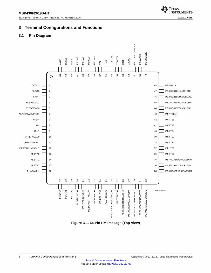
3 Terminal Configurations and Functions
3.1 Pin Diagram
Figure 3-1. 64-Pin PM Package (Top View)
7
MSP430F2619S-HTwww.ti.com SLAS697E –MARCH 2010–REVISED NOVEMBER 2016
Submit Documentation FeedbackProduct Folder Links: MSP430F2619S-HT
Terminal Configurations and FunctionsCopyright © 2010–2016, Texas Instruments Incorporated
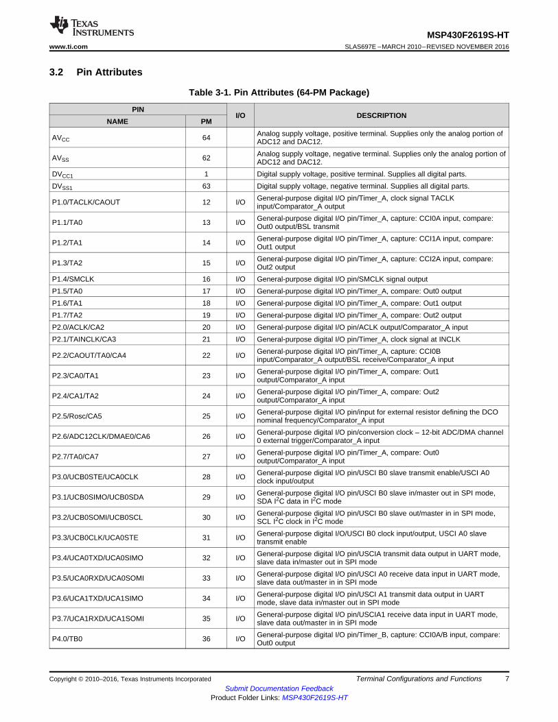
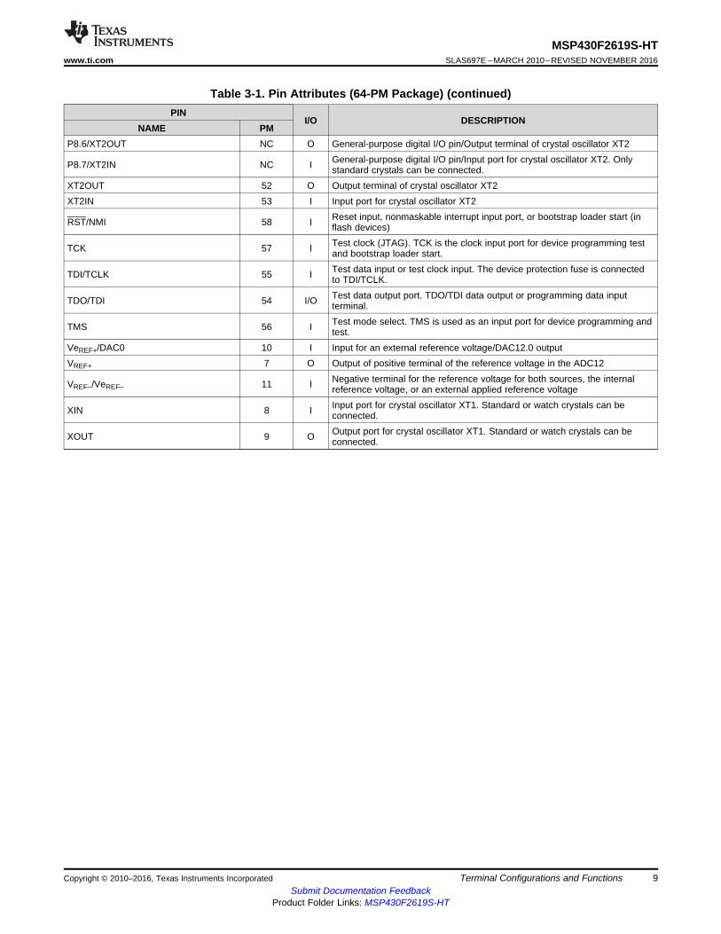
3.2 Pin Attributes
Table 3-1. Pin Attributes (64-PM Package)
PINI/O DESCRIPTION
NAME PM
AVCC 64 Analog supply voltage, positive terminal. Supplies only the analog portion ofADC12 and DAC12.
AVSS 62 Analog supply voltage, negative terminal. Supplies only the analog portion ofADC12 and DAC12.
DVCC1 1 Digital supply voltage, positive terminal. Supplies all digital parts.DVSS1 63 Digital supply voltage, negative terminal. Supplies all digital parts.
P1.0/TACLK/CAOUT 12 I/O General-purpose digital I/O pin/Timer_A, clock signal TACLKinput/Comparator_A output
P1.1/TA0 13 I/O General-purpose digital I/O pin/Timer_A, capture: CCI0A input, compare:Out0 output/BSL transmit
P1.2/TA1 14 I/O General-purpose digital I/O pin/Timer_A, capture: CCI1A input, compare:Out1 output
P1.3/TA2 15 I/O General-purpose digital I/O pin/Timer_A, capture: CCI2A input, compare:Out2 output
P1.4/SMCLK 16 I/O General-purpose digital I/O pin/SMCLK signal outputP1.5/TA0 17 I/O General-purpose digital I/O pin/Timer_A, compare: Out0 outputP1.6/TA1 18 I/O General-purpose digital I/O pin/Timer_A, compare: Out1 outputP1.7/TA2 19 I/O General-purpose digital I/O pin/Timer_A, compare: Out2 outputP2.0/ACLK/CA2 20 I/O General-purpose digital I/O pin/ACLK output/Comparator_A inputP2.1/TAINCLK/CA3 21 I/O General-purpose digital I/O pin/Timer_A, clock signal at INCLK
P2.2/CAOUT/TA0/CA4 22 I/O General-purpose digital I/O pin/Timer_A, capture: CCI0Binput/Comparator_A output/BSL receive/Comparator_A input
P2.3/CA0/TA1 23 I/O General-purpose digital I/O pin/Timer_A, compare: Out1output/Comparator_A input
P2.4/CA1/TA2 24 I/O General-purpose digital I/O pin/Timer_A, compare: Out2output/Comparator_A input
P2.5/Rosc/CA5 25 I/O General-purpose digital I/O pin/input for external resistor defining the DCOnominal frequency/Comparator_A input
P2.6/ADC12CLK/DMAE0/CA6 26 I/O General-purpose digital I/O pin/conversion clock – 12-bit ADC/DMA channel0 external trigger/Comparator_A input
P2.7/TA0/CA7 27 I/O General-purpose digital I/O pin/Timer_A, compare: Out0output/Comparator_A input
P3.0/UCB0STE/UCA0CLK 28 I/O General-purpose digital I/O pin/USCI B0 slave transmit enable/USCI A0clock input/output
P3.1/UCB0SIMO/UCB0SDA 29 I/O General-purpose digital I/O pin/USCI B0 slave in/master out in SPI mode,SDA I2C data in I2C mode
P3.2/UCB0SOMI/UCB0SCL 30 I/O General-purpose digital I/O pin/USCI B0 slave out/master in in SPI mode,SCL I2C clock in I2C mode
P3.3/UCB0CLK/UCA0STE 31 I/O General-purpose digital I/O/USCI B0 clock input/output, USCI A0 slavetransmit enable
P3.4/UCA0TXD/UCA0SIMO 32 I/O General-purpose digital I/O pin/USCIA transmit data output in UART mode,slave data in/master out in SPI mode
P3.5/UCA0RXD/UCA0SOMI 33 I/O General-purpose digital I/O pin/USCI A0 receive data input in UART mode,slave data out/master in in SPI mode
P3.6/UCA1TXD/UCA1SIMO 34 I/O General-purpose digital I/O pin/USCI A1 transmit data output in UARTmode, slave data in/master out in SPI mode
P3.7/UCA1RXD/UCA1SOMI 35 I/O General-purpose digital I/O pin/USCIA1 receive data input in UART mode,slave data out/master in in SPI mode
P4.0/TB0 36 I/O General-purpose digital I/O pin/Timer_B, capture: CCI0A/B input, compare:Out0 output
8
MSP430F2619S-HTSLAS697E –MARCH 2010–REVISED NOVEMBER 2016 www.ti.com
Submit Documentation FeedbackProduct Folder Links: MSP430F2619S-HT
Terminal Configurations and Functions Copyright © 2010–2016, Texas Instruments Incorporated
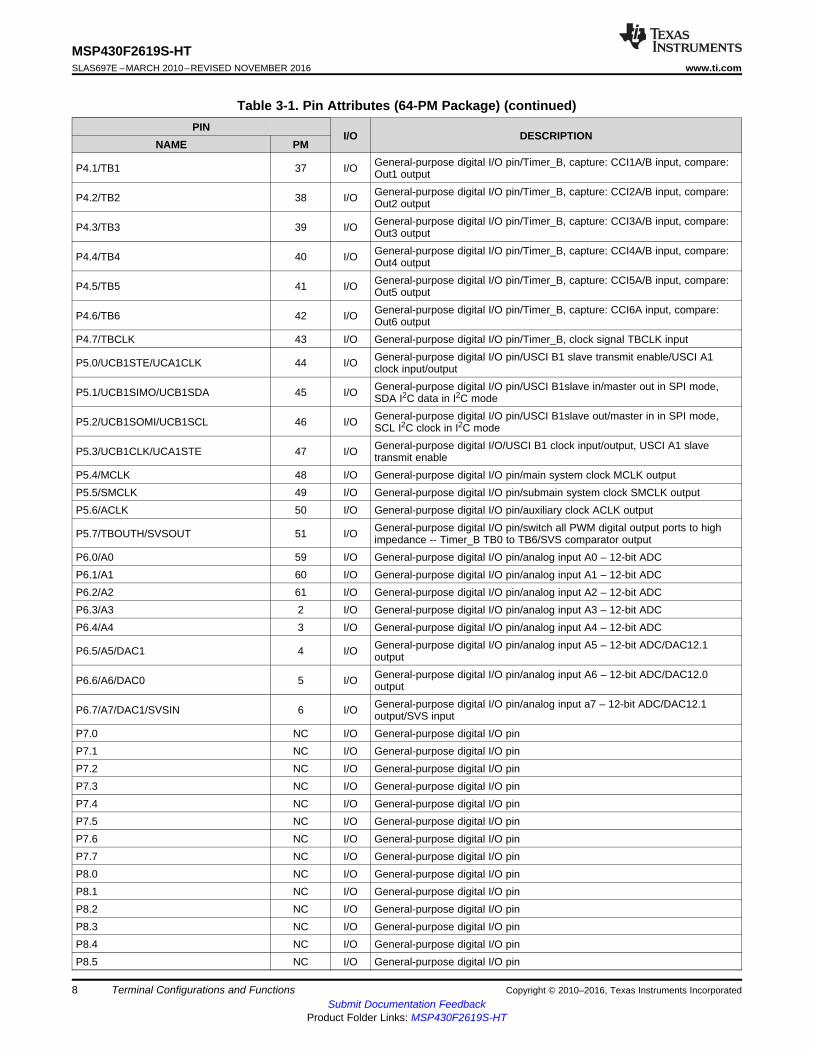
Table 3-1. Pin Attributes (64-PM Package) (continued)PIN
I/O DESCRIPTIONNAME PM
P4.1/TB1 37 I/O General-purpose digital I/O pin/Timer_B, capture: CCI1A/B input, compare:Out1 output
P4.2/TB2 38 I/O General-purpose digital I/O pin/Timer_B, capture: CCI2A/B input, compare:Out2 output
P4.3/TB3 39 I/O General-purpose digital I/O pin/Timer_B, capture: CCI3A/B input, compare:Out3 output
P4.4/TB4 40 I/O General-purpose digital I/O pin/Timer_B, capture: CCI4A/B input, compare:Out4 output
P4.5/TB5 41 I/O General-purpose digital I/O pin/Timer_B, capture: CCI5A/B input, compare:Out5 output
P4.6/TB6 42 I/O General-purpose digital I/O pin/Timer_B, capture: CCI6A input, compare:Out6 output
P4.7/TBCLK 43 I/O General-purpose digital I/O pin/Timer_B, clock signal TBCLK input
P5.0/UCB1STE/UCA1CLK 44 I/O General-purpose digital I/O pin/USCI B1 slave transmit enable/USCI A1clock input/output
P5.1/UCB1SIMO/UCB1SDA 45 I/O General-purpose digital I/O pin/USCI B1slave in/master out in SPI mode,SDA I2C data in I2C mode
P5.2/UCB1SOMI/UCB1SCL 46 I/O General-purpose digital I/O pin/USCI B1slave out/master in in SPI mode,SCL I2C clock in I2C mode
P5.3/UCB1CLK/UCA1STE 47 I/O General-purpose digital I/O/USCI B1 clock input/output, USCI A1 slavetransmit enable
P5.4/MCLK 48 I/O General-purpose digital I/O pin/main system clock MCLK outputP5.5/SMCLK 49 I/O General-purpose digital I/O pin/submain system clock SMCLK outputP5.6/ACLK 50 I/O General-purpose digital I/O pin/auxiliary clock ACLK output
P5.7/TBOUTH/SVSOUT 51 I/O General-purpose digital I/O pin/switch all PWM digital output ports to highimpedance -- Timer_B TB0 to TB6/SVS comparator output
P6.0/A0 59 I/O General-purpose digital I/O pin/analog input A0 – 12-bit ADCP6.1/A1 60 I/O General-purpose digital I/O pin/analog input A1 – 12-bit ADCP6.2/A2 61 I/O General-purpose digital I/O pin/analog input A2 – 12-bit ADCP6.3/A3 2 I/O General-purpose digital I/O pin/analog input A3 – 12-bit ADCP6.4/A4 3 I/O General-purpose digital I/O pin/analog input A4 – 12-bit ADC
P6.5/A5/DAC1 4 I/O General-purpose digital I/O pin/analog input A5 – 12-bit ADC/DAC12.1output
P6.6/A6/DAC0 5 I/O General-purpose digital I/O pin/analog input A6 – 12-bit ADC/DAC12.0output
P6.7/A7/DAC1/SVSIN 6 I/O General-purpose digital I/O pin/analog input a7 – 12-bit ADC/DAC12.1output/SVS input
P7.0 NC I/O General-purpose digital I/O pinP7.1 NC I/O General-purpose digital I/O pinP7.2 NC I/O General-purpose digital I/O pinP7.3 NC I/O General-purpose digital I/O pinP7.4 NC I/O General-purpose digital I/O pinP7.5 NC I/O General-purpose digital I/O pinP7.6 NC I/O General-purpose digital I/O pinP7.7 NC I/O General-purpose digital I/O pinP8.0 NC I/O General-purpose digital I/O pinP8.1 NC I/O General-purpose digital I/O pinP8.2 NC I/O General-purpose digital I/O pinP8.3 NC I/O General-purpose digital I/O pinP8.4 NC I/O General-purpose digital I/O pinP8.5 NC I/O General-purpose digital I/O pin
9
MSP430F2619S-HTwww.ti.com SLAS697E –MARCH 2010–REVISED NOVEMBER 2016
Submit Documentation FeedbackProduct Folder Links: MSP430F2619S-HT
Terminal Configurations and FunctionsCopyright © 2010–2016, Texas Instruments Incorporated
Table 3-1. Pin Attributes (64-PM Package) (continued)PIN
I/O DESCRIPTIONNAME PM
P8.6/XT2OUT NC O General-purpose digital I/O pin/Output terminal of crystal oscillator XT2
P8.7/XT2IN NC I General-purpose digital I/O pin/Input port for crystal oscillator XT2. Onlystandard crystals can be connected.
XT2OUT 52 O Output terminal of crystal oscillator XT2XT2IN 53 I Input port for crystal oscillator XT2
RST/NMI 58 I Reset input, nonmaskable interrupt input port, or bootstrap loader start (inflash devices)
TCK 57 I Test clock (JTAG). TCK is the clock input port for device programming testand bootstrap loader start.
TDI/TCLK 55 I Test data input or test clock input. The device protection fuse is connectedto TDI/TCLK.
TDO/TDI 54 I/O Test data output port. TDO/TDI data output or programming data inputterminal.
TMS 56 I Test mode select. TMS is used as an input port for device programming andtest.
VeREF+/DAC0 10 I Input for an external reference voltage/DAC12.0 outputVREF+ 7 O Output of positive terminal of the reference voltage in the ADC12
VREF–/VeREF– 11 I Negative terminal for the reference voltage for both sources, the internalreference voltage, or an external applied reference voltage
XIN 8 I Input port for crystal oscillator XT1. Standard or watch crystals can beconnected.
XOUT 9 O Output port for crystal oscillator XT1. Standard or watch crystals can beconnected.
10
MSP430F2619S-HTSLAS697E –MARCH 2010–REVISED NOVEMBER 2016 www.ti.com
Submit Documentation FeedbackProduct Folder Links: MSP430F2619S-HT
Terminal Configurations and Functions Copyright © 2010–2016, Texas Instruments Incorporated
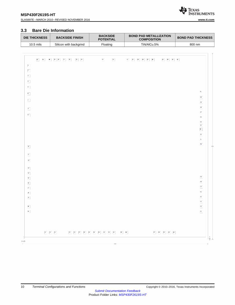
3.3 Bare Die InformationDIE THICKNESS BACKSIDE FINISH BACKSIDE
POTENTIALBOND PAD METALLIZATION
COMPOSITION BOND PAD THICKNESS
10.5 mils Silicon with backgrind Floating TiN/AlCu.5% 800 nm
11
MSP430F2619S-HTwww.ti.com SLAS697E –MARCH 2010–REVISED NOVEMBER 2016
Submit Documentation FeedbackProduct Folder Links: MSP430F2619S-HT
Terminal Configurations and FunctionsCopyright © 2010–2016, Texas Instruments Incorporated
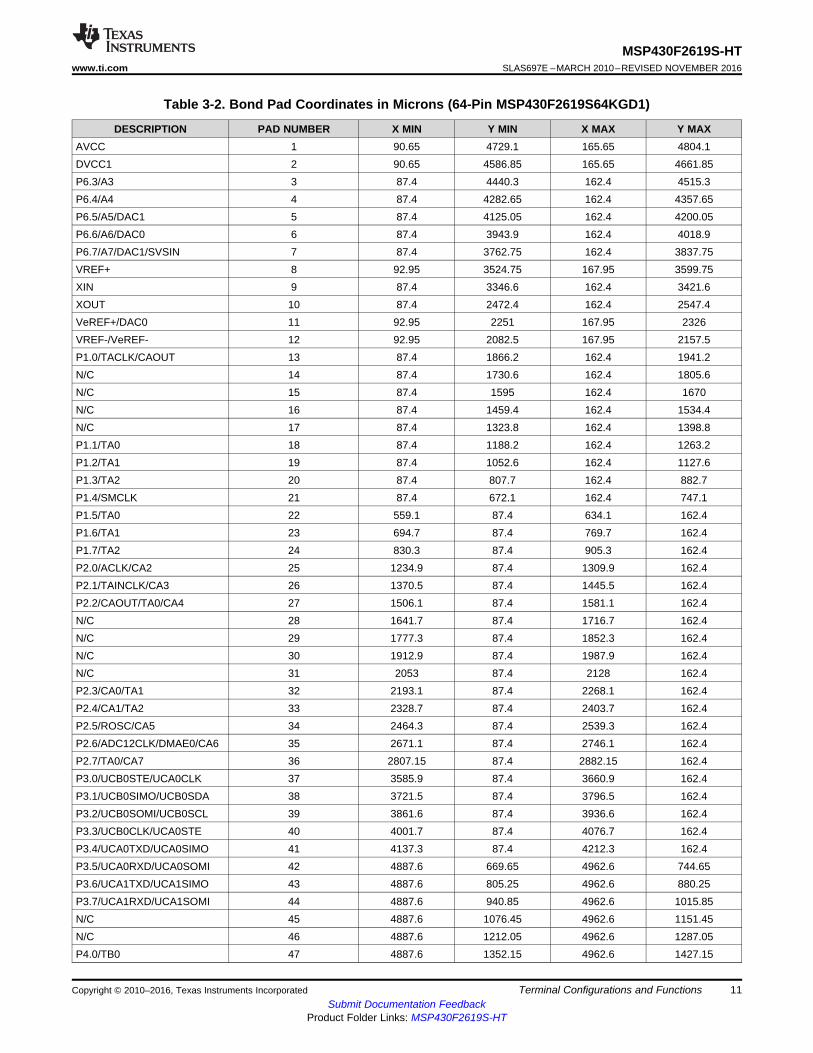
Table 3-2. Bond Pad Coordinates in Microns (64-Pin MSP430F2619S64KGD1)
DESCRIPTION PAD NUMBER X MIN Y MIN X MAX Y MAXAVCC 1 90.65 4729.1 165.65 4804.1DVCC1 2 90.65 4586.85 165.65 4661.85P6.3/A3 3 87.4 4440.3 162.4 4515.3P6.4/A4 4 87.4 4282.65 162.4 4357.65P6.5/A5/DAC1 5 87.4 4125.05 162.4 4200.05P6.6/A6/DAC0 6 87.4 3943.9 162.4 4018.9P6.7/A7/DAC1/SVSIN 7 87.4 3762.75 162.4 3837.75VREF+ 8 92.95 3524.75 167.95 3599.75XIN 9 87.4 3346.6 162.4 3421.6XOUT 10 87.4 2472.4 162.4 2547.4VeREF+/DAC0 11 92.95 2251 167.95 2326VREF-/VeREF- 12 92.95 2082.5 167.95 2157.5P1.0/TACLK/CAOUT 13 87.4 1866.2 162.4 1941.2N/C 14 87.4 1730.6 162.4 1805.6N/C 15 87.4 1595 162.4 1670N/C 16 87.4 1459.4 162.4 1534.4N/C 17 87.4 1323.8 162.4 1398.8P1.1/TA0 18 87.4 1188.2 162.4 1263.2P1.2/TA1 19 87.4 1052.6 162.4 1127.6P1.3/TA2 20 87.4 807.7 162.4 882.7P1.4/SMCLK 21 87.4 672.1 162.4 747.1P1.5/TA0 22 559.1 87.4 634.1 162.4P1.6/TA1 23 694.7 87.4 769.7 162.4P1.7/TA2 24 830.3 87.4 905.3 162.4P2.0/ACLK/CA2 25 1234.9 87.4 1309.9 162.4P2.1/TAINCLK/CA3 26 1370.5 87.4 1445.5 162.4P2.2/CAOUT/TA0/CA4 27 1506.1 87.4 1581.1 162.4N/C 28 1641.7 87.4 1716.7 162.4N/C 29 1777.3 87.4 1852.3 162.4N/C 30 1912.9 87.4 1987.9 162.4N/C 31 2053 87.4 2128 162.4P2.3/CA0/TA1 32 2193.1 87.4 2268.1 162.4P2.4/CA1/TA2 33 2328.7 87.4 2403.7 162.4P2.5/ROSC/CA5 34 2464.3 87.4 2539.3 162.4P2.6/ADC12CLK/DMAE0/CA6 35 2671.1 87.4 2746.1 162.4P2.7/TA0/CA7 36 2807.15 87.4 2882.15 162.4P3.0/UCB0STE/UCA0CLK 37 3585.9 87.4 3660.9 162.4P3.1/UCB0SIMO/UCB0SDA 38 3721.5 87.4 3796.5 162.4P3.2/UCB0SOMI/UCB0SCL 39 3861.6 87.4 3936.6 162.4P3.3/UCB0CLK/UCA0STE 40 4001.7 87.4 4076.7 162.4P3.4/UCA0TXD/UCA0SIMO 41 4137.3 87.4 4212.3 162.4P3.5/UCA0RXD/UCA0SOMI 42 4887.6 669.65 4962.6 744.65P3.6/UCA1TXD/UCA1SIMO 43 4887.6 805.25 4962.6 880.25P3.7/UCA1RXD/UCA1SOMI 44 4887.6 940.85 4962.6 1015.85N/C 45 4887.6 1076.45 4962.6 1151.45N/C 46 4887.6 1212.05 4962.6 1287.05P4.0/TB0 47 4887.6 1352.15 4962.6 1427.15
12
MSP430F2619S-HTSLAS697E –MARCH 2010–REVISED NOVEMBER 2016 www.ti.com
Submit Documentation FeedbackProduct Folder Links: MSP430F2619S-HT
Terminal Configurations and Functions Copyright © 2010–2016, Texas Instruments Incorporated
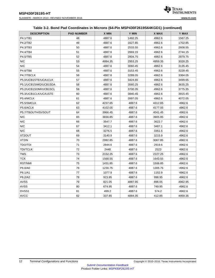
Table 3-2. Bond Pad Coordinates in Microns (64-Pin MSP430F2619S64KGD1) (continued)DESCRIPTION PAD NUMBER X MIN Y MIN X MAX Y MAX
P4.1/TB1 48 4887.6 1492.25 4962.6 1567.25P4.2/TB2 49 4887.6 1627.85 4962.6 1702.85P4.3/TB3 50 4887.6 2533.55 4962.6 2608.55P4.4/TB4 51 4887.6 2669.15 4962.6 2744.15P4.5/TB5 52 4887.6 2804.75 4962.6 2879.75N/C 53 4884.35 2953.25 4959.35 3028.25N/C 54 4887.6 3060.45 4962.6 3135.45P4.6/TB6 55 4887.6 3153.45 4962.6 3228.45P4.7/TBCLK 56 4887.6 3289.05 4962.6 3364.05P5.0/UCB1STE/UCA1CLK 57 4887.6 3424.65 4962.6 3499.65P5.1/UCB1SIMO/UCB1SDA 58 4887.6 3560.25 4962.6 3635.25P5.2/UCB1SOMI/UCB1SCL 59 4887.6 3700.35 4962.6 3775.35P5.3/UCB1CLK/UCA1STE 60 4887.6 3840.45 4962.6 3915.45P5.4/MCLK 61 4887.6 3997.05 4962.6 4072.05P5.5/SMCLK 62 4237.65 4887.6 4312.65 4962.6P5.6/ACLK 63 4102.05 4887.6 4177.05 4962.6P5.7/TBOUTH/SVSOUT 64 3966.45 4887.6 4041.45 4962.6N/C 65 3830.85 4887.6 3905.85 4962.6N/C 66 3547.7 4887.6 3622.7 4962.6N/C 67 3412.1 4887.6 3487.1 4962.6N/C 68 3276.5 4887.6 3351.5 4962.6XT2OUT 69 3140.9 4887.6 3215.9 4962.6XT2IN 70 2992.85 4887.6 3067.85 4962.6TDO/TDI 71 2844.6 4887.6 2919.6 4962.6TDI/TCLK 72 2448 4887.6 2523 4962.6TMS 73 2152.25 4887.6 2227.25 4962.6TCK 74 1568.55 4887.6 1643.55 4962.6RST/NMI 75 1431.85 4887.6 1506.85 4962.6P6.0/A0 76 1230.75 4887.6 1305.75 4962.6P6.1/A1 77 1077.9 4887.6 1152.9 4962.6P6.2/A2 78 923.95 4887.6 998.95 4962.6AVSS 79 821.05 4887.95 896.05 4962.95AVSS 80 674.95 4887.6 749.95 4962.6DVSS1 81 499.2 4887.6 574.2 4962.6AVCC 82 337.85 4884.35 412.85 4959.35
13
MSP430F2619S-HTwww.ti.com SLAS697E –MARCH 2010–REVISED NOVEMBER 2016
Submit Documentation FeedbackProduct Folder Links: MSP430F2619S-HT
Terminal Configurations and FunctionsCopyright © 2010–2016, Texas Instruments Incorporated
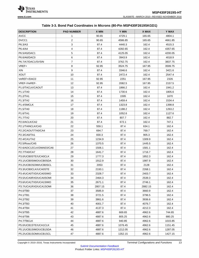
Table 3-3. Bond Pad Coordinates in Microns (80-Pin MSP430F2619SKGD1)
DESCRIPTION PAD NUMBER X MIN Y MIN X MAX Y MAXAVCC 1 90.65 4729.1 165.65 4804.1DVCC1 2 90.65 4586.85 165.65 4661.85P6.3/A3 3 87.4 4440.3 162.4 4515.3P6.4/A4 4 87.4 4282.65 162.4 4357.65P6.5/A5/DAC1 5 87.4 4125.05 162.4 4200.05P6.6/A6/DAC0 6 87.4 3943.9 162.4 4018.9P6.7/A7/DAC1/SVSIN 7 87.4 3762.75 162.4 3837.75VREF+ 8 92.95 3524.75 167.95 3599.75XIN 9 87.4 3346.6 162.4 3421.6XOUT 10 87.4 2472.4 162.4 2547.4VeREF+/DAC0 11 92.95 2251 167.95 2326VREF-/VeREF- 12 92.95 2082.5 167.95 2157.5P1.0/TACLK/CAOUT 13 87.4 1866.2 162.4 1941.2P1.1/TA0 14 87.4 1730.6 162.4 1805.6P1.2/TA1 15 87.4 1595 162.4 1670P1.3/TA2 16 87.4 1459.4 162.4 1534.4P1.4/SMCLK 17 87.4 1323.8 162.4 1398.8P1.5/TA0 18 87.4 1188.2 162.4 1263.2P1.6/TA1 19 87.4 1052.6 162.4 1127.6P1.7/TA2 20 87.4 807.7 162.4 882.7P2.0/ACLK/CA2 21 87.4 672.1 162.4 747.1P2.1/TAINCLK/CA3 22 559.1 87.4 634.1 162.4P2.2/CAOUT/TA0/CA4 23 694.7 87.4 769.7 162.4P2.3/CA0/TA1 24 830.3 87.4 905.3 162.4P2.4/CA1/TA2 25 1234.9 87.4 1309.9 162.4P2.5/Rosc/CA5 26 1370.5 87.4 1445.5 162.4P2.6/ADC12CLK/DMAE0/CA6 27 1506.1 87.4 1581.1 162.4P2.7/TA0/CA7 28 1641.7 87.4 1716.7 162.4P3.0/UCB0STE/UCA0CLK 29 1777.3 87.4 1852.3 162.4P3.1/UCB0SIMO/UCB0SDA 30 1912.9 87.4 1987.9 162.4P3.2/UCBOSOMI/UCB0SCL 31 2053 87.4 2128 162.4P3.3/UCB0CLK/UCA0STE 32 2193.1 87.4 2268.1 162.4P3.4/UCA0TXD/UCA0SIMO 33 2328.7 87.4 2403.7 162.4P3.5/UCA0RXD/UCA0SOMI 34 2464.3 87.4 2539.3 162.4P3.6/UCA1TXD/UCA1SIMO 35 2671.1 87.4 2746.1 162.4P3.7/UCA1RXD/UCA1SOMI 36 2807.15 87.4 2882.15 162.4P4.0/TB0 37 3585.9 87.4 3660.9 162.4P4.1/TB1 38 3721.5 87.4 3796.5 162.4P4.2/TB2 39 3861.6 87.4 3936.6 162.4P4.3/TB3 40 4001.7 87.4 4076.7 162.4P4.4/TB4 41 4137.3 87.4 4212.3 162.4P4.5/TB5 42 4887.6 669.65 4962.6 744.65P4.6/TB6 43 4887.6 805.25 4962.6 880.25P4.7/TBCLK 44 4887.6 940.85 4962.6 1015.85P5.0/UCB1STE/UCA1CLK 45 4887.6 1076.45 4962.6 1151.45P5.1/UCB1SIMO/UCB1SDA 46 4887.6 1212.05 4962.6 1287.05P5.2/UCB1SOMI/UCB1SCL 47 4887.6 1352.15 4962.6 1427.15
14
MSP430F2619S-HTSLAS697E –MARCH 2010–REVISED NOVEMBER 2016 www.ti.com
Submit Documentation FeedbackProduct Folder Links: MSP430F2619S-HT
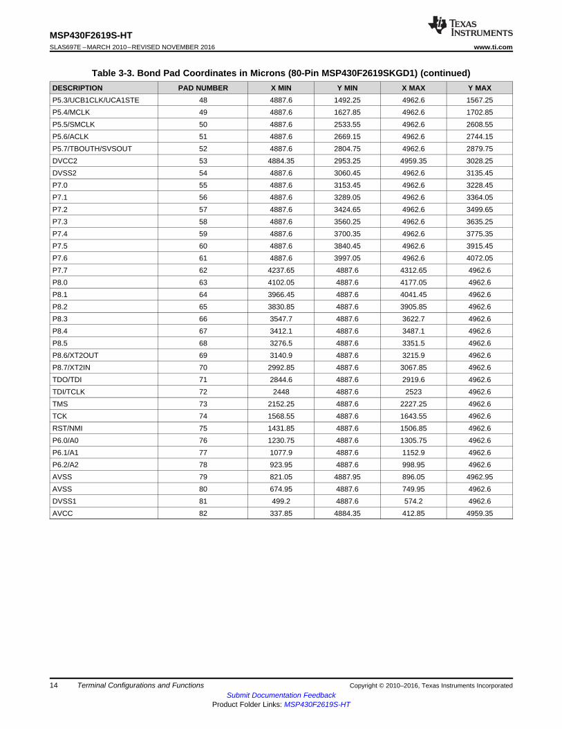
Terminal Configurations and Functions Copyright © 2010–2016, Texas Instruments Incorporated
Table 3-3. Bond Pad Coordinates in Microns (80-Pin MSP430F2619SKGD1) (continued)DESCRIPTION PAD NUMBER X MIN Y MIN X MAX Y MAXP5.3/UCB1CLK/UCA1STE 48 4887.6 1492.25 4962.6 1567.25P5.4/MCLK 49 4887.6 1627.85 4962.6 1702.85P5.5/SMCLK 50 4887.6 2533.55 4962.6 2608.55P5.6/ACLK 51 4887.6 2669.15 4962.6 2744.15P5.7/TBOUTH/SVSOUT 52 4887.6 2804.75 4962.6 2879.75DVCC2 53 4884.35 2953.25 4959.35 3028.25DVSS2 54 4887.6 3060.45 4962.6 3135.45P7.0 55 4887.6 3153.45 4962.6 3228.45P7.1 56 4887.6 3289.05 4962.6 3364.05P7.2 57 4887.6 3424.65 4962.6 3499.65P7.3 58 4887.6 3560.25 4962.6 3635.25P7.4 59 4887.6 3700.35 4962.6 3775.35P7.5 60 4887.6 3840.45 4962.6 3915.45P7.6 61 4887.6 3997.05 4962.6 4072.05P7.7 62 4237.65 4887.6 4312.65 4962.6P8.0 63 4102.05 4887.6 4177.05 4962.6P8.1 64 3966.45 4887.6 4041.45 4962.6P8.2 65 3830.85 4887.6 3905.85 4962.6P8.3 66 3547.7 4887.6 3622.7 4962.6P8.4 67 3412.1 4887.6 3487.1 4962.6P8.5 68 3276.5 4887.6 3351.5 4962.6P8.6/XT2OUT 69 3140.9 4887.6 3215.9 4962.6P8.7/XT2IN 70 2992.85 4887.6 3067.85 4962.6TDO/TDI 71 2844.6 4887.6 2919.6 4962.6TDI/TCLK 72 2448 4887.6 2523 4962.6TMS 73 2152.25 4887.6 2227.25 4962.6TCK 74 1568.55 4887.6 1643.55 4962.6RST/NMI 75 1431.85 4887.6 1506.85 4962.6P6.0/A0 76 1230.75 4887.6 1305.75 4962.6P6.1/A1 77 1077.9 4887.6 1152.9 4962.6P6.2/A2 78 923.95 4887.6 998.95 4962.6AVSS 79 821.05 4887.95 896.05 4962.95AVSS 80 674.95 4887.6 749.95 4962.6DVSS1 81 499.2 4887.6 574.2 4962.6AVCC 82 337.85 4884.35 412.85 4959.35
15
MSP430F2619S-HTwww.ti.com SLAS697E –MARCH 2010–REVISED NOVEMBER 2016
Submit Documentation FeedbackProduct Folder Links: MSP430F2619S-HT
SpecificationsCopyright © 2010–2016, Texas Instruments Incorporated
(1) Stresses beyond those listed under Absolute Maximum Ratings may cause permanent damage to the device. These are stress ratingsonly, and functional operation of the device at these or any other conditions beyond those indicated under Recommended OperatingConditions is not implied. Exposure to absolute-maximum-rated conditions for extended periods may affect device reliability.
(2) All voltages referenced to VSS. The JTAG fuse-blow voltage, VFB, is allowed to exceed the absolute maximum rating. The voltage isapplied to the TEST pin when blowing the JTAG fuse.
(3) Higher temperature may be applied during board soldering process according to the current JEDEC J-STD-020 specification with peakreflow temperatures not higher than classified on the device label on the shipping boxes or reels.
4 Specifications
4.1 Absolute Maximum Ratings (1)
MIN MAX UNITVoltage applied at VCC to VSS –0.3 4.1 VVoltage applied to any pin (2) –0.3 VCC + 0.3 VDiode current at any device terminal –2 2 mA
TstgStorage temperature (unprogrammed device (3)) –55 150
°CStorage temperature (programmed device (3)) –55 150
(1) JEDEC document JEP155 states that 500-V HBM allows safe manufacturing with a standard ESD control process.(2) JEDEC document JEP157 states that 250-V CDM allows safe manufacturing with a standard ESD control process.
4.2 ESD RatingsMAX UNIT
V(ESD) Electrostatic dischargeHuman-body model (HBM), per ANSI/ESDA/JEDEC JS001 (1) ±4000
VCharged-device model (CDM), per JESD22-C101 (2) ±750
(1) The MSP430 CPU is clocked directly with MCLK. Both the high and low phase of MCLK must not exceed the pulse width of thespecified maximum frequency.
(2) Modules might have a different maximum input clock specification. Refer to the specification of the respective module in this data sheet.(3) It is recommended to power AVCC and DVCC from the same source. A maximum difference of 0.3 V between AVCC and DVCC can be
tolerated during power-up.
4.3 Recommended Operating Conditions (1) (2)
MIN NOM MAX UNIT
VCC
Supply voltage during program executionAVCC = DVCC = VCC
(3)1.8 3.6
VSupply voltage during flash memoryprogramming 2.2 3.6
VSS Supply voltage AVSS = DVSS = VSS 0 VTA Operating free-air temperature range –55 150 °C
Processor frequency ƒSYSTEM(Maximum MCLK frequency) (1) (2)
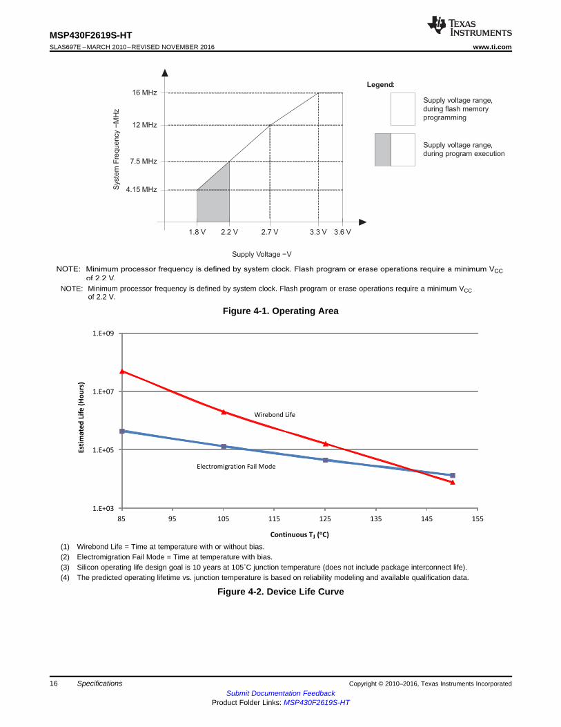
(see Figure 4-1)
VCC = 2.2 V, duty cycle = 50% ±10% DC 10MHzVCC = 2.7 V, duty cycle = 50% ±10% DC 12
VCC ≥ 3.3 V, duty cycle = 50% ±10% DC 16
1.E+03
1.E+05
1.E+07
1.E+09
85 95 105 115 125 135 145 155
Est
ima
ted
Lif
e (
Ho
urs
)
Continuous TJ (oC)
Electromigration Fail Mode
Wirebond Life
4.15 MHz
12 MHz
16 MHz
1.8 V 2.2 V 2.7 V 3.3 V 3.6 V
Supply Voltage −V
Syste
mF
requency
−M
Hz
Supply voltage range,during flash memoryprogramming
Supply voltage range,during program execution
Legend:
7.5 MHz
NOTE: Minimum processor frequency is defined by system clock. Flash program or erase operations require a minimum VCC
of 2.2 V.
16
MSP430F2619S-HTSLAS697E –MARCH 2010–REVISED NOVEMBER 2016 www.ti.com
Submit Documentation FeedbackProduct Folder Links: MSP430F2619S-HT
Specifications Copyright © 2010–2016, Texas Instruments Incorporated
NOTE: Minimum processor frequency is defined by system clock. Flash program or erase operations require a minimum VCCof 2.2 V.
Figure 4-1. Operating Area
(1) Wirebond Life = Time at temperature with or without bias.(2) Electromigration Fail Mode = Time at temperature with bias.(3) Silicon operating life design goal is 10 years at 105˚C junction temperature (does not include package interconnect life).(4) The predicted operating lifetime vs. junction temperature is based on reliability modeling and available qualification data.
Figure 4-2. Device Life Curve
17
MSP430F2619S-HTwww.ti.com SLAS697E –MARCH 2010–REVISED NOVEMBER 2016
Submit Documentation FeedbackProduct Folder Links: MSP430F2619S-HT
SpecificationsCopyright © 2010–2016, Texas Instruments Incorporated
(1) For more information about traditional and new thermal metrics, see the Semiconductor and IC Package Thermal Metrics applicationreport.
4.4 Thermal Information
THERMAL METRIC (1)MSP430F2619S-HT
UNITPM (QFP)64 PINS
RθJA Junction-to-ambient thermal resistance 48.7 °C/WRθJC(top) Junction-to-case (top) thermal resistance 9.9 °C/WRθJB Junction-to-board thermal resistance 22.4 °C/WψJT Junction-to-top characterization parameter 0.4 °C/WψJB Junction-to-board characterization parameter 21.9 °C/W
(1) All inputs are tied to 0 V or VCC. Outputs do not source or sink any current.(2) The currents are characterized with a Micro Crystal CC4V-T1A SMD crystal with a load capacitance of 9 pF. The internal and external
load capacitance is chosen to closely match the required 9 pF.
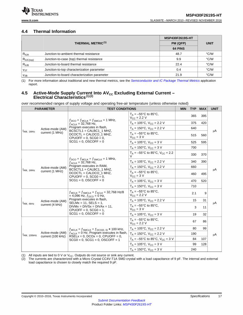
4.5 Active-Mode Supply Current Into AVCC Excluding External Current –Electrical Characteristics (1) (2)
over recommended ranges of supply voltage and operating free-air temperature (unless otherwise noted)PARAMETER TEST CONDITIONS MIN TYP MAX UNIT
IAM, 1MHzActive-mode (AM)current (1 MHz)
ƒDCO = ƒMCLK = ƒSMCLK = 1 MHz,ƒACLK = 32,768 Hz,Program executes in flash,BCSCTL1 = CALBC1_1 MHZ,DCOCTL = CALDCO_1 MHZ,CPUOFF = 0, SCG0 = 0,SCG1 = 0, OSCOFF = 0
TA = –55°C to 85°C,VCC = 2.2 V 365 395
μA
TA = 105°C, VCC = 2.2 V 375 420TA = 150°C, VCC = 2.2 V 640TA = –55°C to 85°C,VCC = 3 V 515 560
TA = 105°C, VCC = 3 V 525 595TA = 150°C, VCC = 3 V 700
IAM, 1MHzActive-mode (AM)current (1 MHz)
ƒDCO = ƒMCLK = ƒSMCLK = 1 MHz,ƒACLK = 32,768 Hz,Program executes in RAM,BCSCTL1 = CALBC1_1 MHZ,DCOCTL = CALDCO_1 MHZ,CPUOFF = 0, SCG0 = 0,SCG1 = 0, OSCOFF = 0
TA = –55°C to 85°C, VCC = 2.2V 330 370
μA
TA = 105°C, VCC = 2.2 V 340 390TA = 150°C, VCC = 2.2 V 660TA = –55°C to 85°C,VCC = 3 V 460 495
TA = 105°C, VCC = 3 V 470 520TA = 150°C, VCC = 3 V 710
IAM, 4kHzActive-mode (AM)current (4 kHz)
ƒMCLK = ƒSMCLK = ƒACLK = 32,768 Hz/8= 4,096 Hz, ƒDCO = 0 Hz,Program executes in flash,SELMx = 11, SELS = 1,DIVMx = DIVSx = DIVAx = 11,CPUOFF = 0, SCG0 = 1,SCG1 = 0, OSCOFF = 0
TA = –55°C to 85°C,VCC = 2.2 V 2.1 9
μATA = 105°C, VCC = 2.2 V 15 31TA = –55°C to 85°C,VCC = 3 V 3 11
TA = 105°C, VCC = 3 V 19 32
IAM, 100kHzActive-mode (AM)current (100 kHz)
ƒMCLK = ƒSMCLK = ƒDCO(0, 0) ≉ 100 kHz,ƒACLK = 0 Hz, Program executes in flash,RSELx = 0, DCOx = 0, CPUOFF = 0,SCG0 = 0, SCG1 = 0, OSCOFF = 1
TA = –55°C to 85°C,VCC = 2.2 V 67 86
μA
TA = 105°C, VCC = 2.2 V 80 99TA = 150°C, VCC = 2.2 V 190TA = –55°C to 85°C, VCC = 3 V 84 107TA = 105°C, VCC = 3 V 99 128TA = 150°C, VCC = 3 V 240
18
MSP430F2619S-HTSLAS697E –MARCH 2010–REVISED NOVEMBER 2016 www.ti.com
Submit Documentation FeedbackProduct Folder Links: MSP430F2619S-HT
Specifications Copyright © 2010–2016, Texas Instruments Incorporated
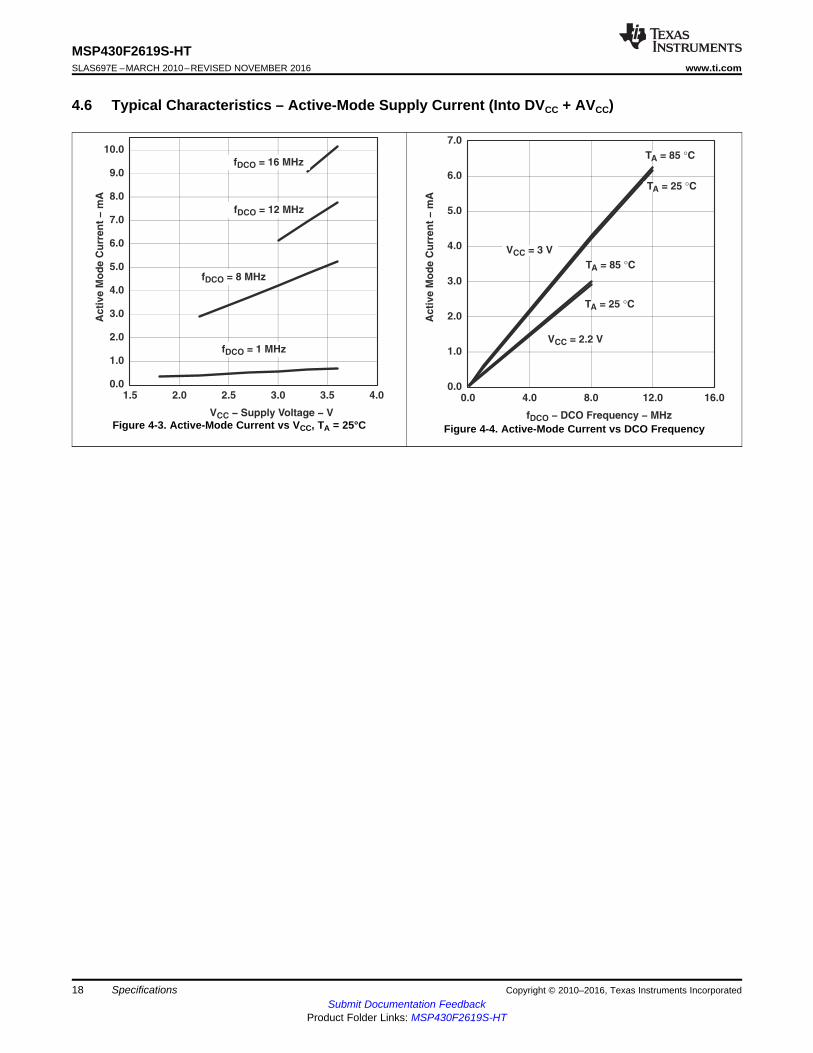
4.6 Typical Characteristics – Active-Mode Supply Current (Into DVCC + AVCC)
Figure 4-3. Active-Mode Current vs VCC, TA = 25°C Figure 4-4. Active-Mode Current vs DCO Frequency
19
MSP430F2619S-HTwww.ti.com SLAS697E –MARCH 2010–REVISED NOVEMBER 2016
Submit Documentation FeedbackProduct Folder Links: MSP430F2619S-HT
SpecificationsCopyright © 2010–2016, Texas Instruments Incorporated
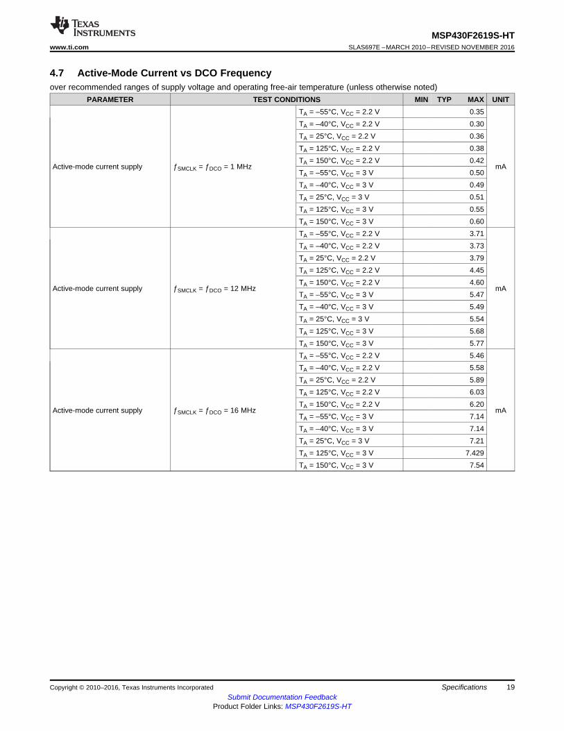
4.7 Active-Mode Current vs DCO Frequencyover recommended ranges of supply voltage and operating free-air temperature (unless otherwise noted)
PARAMETER TEST CONDITIONS MIN TYP MAX UNIT
Active-mode current supply ƒSMCLK = ƒDCO = 1 MHz
TA = –55°C, VCC = 2.2 V 0.35
mA
TA = –40°C, VCC = 2.2 V 0.30TA = 25°C, VCC = 2.2 V 0.36TA = 125°C, VCC = 2.2 V 0.38TA = 150°C, VCC = 2.2 V 0.42TA = –55°C, VCC = 3 V 0.50TA = –40°C, VCC = 3 V 0.49TA = 25°C, VCC = 3 V 0.51TA = 125°C, VCC = 3 V 0.55TA = 150°C, VCC = 3 V 0.60
Active-mode current supply ƒSMCLK = ƒDCO = 12 MHz
TA = –55°C, VCC = 2.2 V 3.71
mA
TA = –40°C, VCC = 2.2 V 3.73TA = 25°C, VCC = 2.2 V 3.79TA = 125°C, VCC = 2.2 V 4.45TA = 150°C, VCC = 2.2 V 4.60TA = –55°C, VCC = 3 V 5.47TA = –40°C, VCC = 3 V 5.49TA = 25°C, VCC = 3 V 5.54TA = 125°C, VCC = 3 V 5.68TA = 150°C, VCC = 3 V 5.77
Active-mode current supply ƒSMCLK = ƒDCO = 16 MHz
TA = –55°C, VCC = 2.2 V 5.46
mA
TA = –40°C, VCC = 2.2 V 5.58TA = 25°C, VCC = 2.2 V 5.89TA = 125°C, VCC = 2.2 V 6.03TA = 150°C, VCC = 2.2 V 6.20TA = –55°C, VCC = 3 V 7.14TA = –40°C, VCC = 3 V 7.14TA = 25°C, VCC = 3 V 7.21TA = 125°C, VCC = 3 V 7.429TA = 150°C, VCC = 3 V 7.54
20
MSP430F2619S-HTSLAS697E –MARCH 2010–REVISED NOVEMBER 2016 www.ti.com
Submit Documentation FeedbackProduct Folder Links: MSP430F2619S-HT
Specifications Copyright © 2010–2016, Texas Instruments Incorporated
(1) All inputs are tied to 0 V or VCC. Outputs do not source or sink any current.(2) The currents are characterized with a Micro Crystal CC4V-T1A SMD crystal with a load capacitance of 9 pF.
The internal and external load capacitance is chosen to closely match the required 9 pF.(3) Current for brownout and WDT clocked by SMCLK included.(4) Current for brownout and WDT clocked by ACLK included.
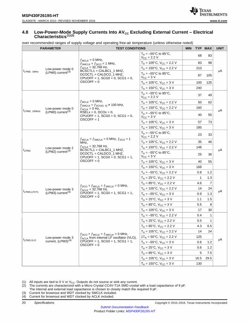
4.8 Low-Power-Mode Supply Currents Into AVCC Excluding External Current – ElectricalCharacteristics (1) (2)
over recommended ranges of supply voltage and operating free-air temperature (unless otherwise noted)PARAMETER TEST CONDITIONS MIN TYP MAX UNIT
ILPM0, 1MHzLow-power mode 0(LPM0) current (3)
ƒMCLK = 0 MHz,ƒSMCLK = ƒDCO = 1 MHz,ƒACLK = 32,768 Hz,BCSCTL1 = CALBC1_1 MHZ,DCOCTL = CALDCO_1 MHZ,CPUOFF = 1, SCG0 = 0, SCG1 = 0,OSCOFF = 0
TA = –55°C to 85°C,VCC = 2.2 V 68 83
μA
TA = 105°C, VCC = 2.2 V 83 98TA = 150°C, VCC = 2.2 V 210TA = –55°C to 85°C,VCC = 3 V 87 105
TA = 105°C, VCC = 3 V 100 125TA = 150°C, VCC = 3 V 240
ILPM0, 100kHzLow-power mode 0(LPM0) current (3)
ƒMCLK = 0 MHz,ƒSMCLK = ƒDCO(0, 0) ≉ 100 kHz,ƒACLK = 0 Hz,RSELx = 0, DCOx = 0,CPUOFF = 1, SCG0 = 0, SCG1 = 0,OSCOFF = 1
TA = –55°C to 85°C,VCC = 2.2 V 37 49
μA
TA = 105°C, VCC = 2.2 V 50 62TA = 150°C, VCC = 2.2 V 160TA = –55°C to 85°C,VCC = 3 V 40 55
TA = 105°C, VCC = 3 V 57 73TA = 150°C, VCC = 3 V 185
ILPM2Low-power mode 2(LPM2) current (4)
ƒMCLK = ƒSMCLK = 0 MHz, ƒDCO = 1MHz,ƒACLK = 32,768 Hz,BCSCTL1 = CALBC1_1 MHZ,DCOCTL = CALDCO_1 MHZ,CPUOFF = 1, SCG0 = 0, SCG1 = 1,OSCOFF = 0
TA = –55°C to 85°C,VCC = 2.2 V 23 33
μA
TA = 105°C, VCC = 2.2 V 35 46TA = 150°C, VCC = 2.2 V 148TA = –55°C to 85°C,VCC = 3 V 25 36
TA = 105°C, VCC = 3 V 40 55TA = 150°C, VCC = 3 V 168
ILPM3,LFXT1Low-power mode 3(LPM3) current (4)
ƒDCO = ƒMCLK = ƒSMCLK = 0 MHz,ƒACLK = 32,768 Hz,CPUOFF = 1, SCG0 = 1, SCG1 = 1,OSCOFF = 0
TA = –55°C, VCC = 2.2 V 0.8 1.2
μA
TA = 25°C, VCC = 2.2 V 1 1.3TA = 85°C, VCC = 2.2 V 4.6 7TA = 105°C, VCC = 2.2 V 14 24TA = –55°C, VCC = 3 V 0.9 1.3TA = 25°C, VCC = 3 V 1.1 1.5TA = 85°C, VCC = 3 V 5.5 8TA = 105°C, VCC = 3 V 17 30
ILPM3,VLOLow-power mode 3current, (LPM3) (4)
ƒDCO = ƒMCLK = ƒSMCLK = 0 MHz,ƒACLK from internal LF oscillator (VLO),CPUOFF = 1, SCG0 = 1, SCG1 = 1,OSCOFF = 0
TA = –55°C, VCC = 2.2 V 0.4 1
μA
TA = 25°C, VCC = 2.2 V 0.5 1TA = 85°C, VCC = 2.2 V 4.3 6.5TA = 105°C, VCC = 2.2 V 14 241TA = 50°C, VCC = 2.2 V 125TA = –55°C, VCC = 3 V 0.6 1.2TA = 25°C, VCC = 3 V 0.6 1.2TA = 85°C, VCC = 3 V 5 7.5TA = 105°C, VCC = 3 V 16.5 29.5TA = 150°C, VCC = 3 V 130
I-
Lo
w-P
ow
er
Mo
de C
urr
en
t -
AL
PM
4m
T - Temperature - °CA
0
1
2
3
4
5
6
7
8
9
10
11
12
13
14
15
16
–40 –20 0 20 40 60 80 100 120
V = 3.6 VCC
V = 30 VCC
V = 2.2 VCC
V = 1.8 VCC
21
MSP430F2619S-HTwww.ti.com SLAS697E –MARCH 2010–REVISED NOVEMBER 2016
Submit Documentation FeedbackProduct Folder Links: MSP430F2619S-HT
SpecificationsCopyright © 2010–2016, Texas Instruments Incorporated
Low-Power-Mode Supply Currents Into AVCC Excluding External Current – ElectricalCharacteristics(1)(2) (continued)over recommended ranges of supply voltage and operating free-air temperature (unless otherwise noted)
PARAMETER TEST CONDITIONS MIN TYP MAX UNIT
(5) Current for brownout included.
ILPM4Low-power mode 4(LPM4) current (5)
ƒDCO = ƒMCLK = ƒSMCLK = 0 MHz,ƒACLK = 0 Hz,CPUOFF = 1, SCG0 = 1, SCG1 = 1,OSCOFF = 1
TA = –55°C, VCC = 2.2 V 0.1 0.5
μA
TA = 25°C, VCC = 2.2 V 0.1 0.5TA = 85°C, VCC = 2.2 V 4 6TA = 105°C, VCC = 2.2 V 13 23TA = 150°C, VCC = 2.2 V 125TA = –55°C, VCC = 3 V 0.2 0.5TA = 25°C, VCC = 3 V 0.2 0.5TA = 85°C, VCC = 3 V 4.7 7TA = 105°C, VCC = 3 V 14 24TA = 150°C, VCC = 3 V 146
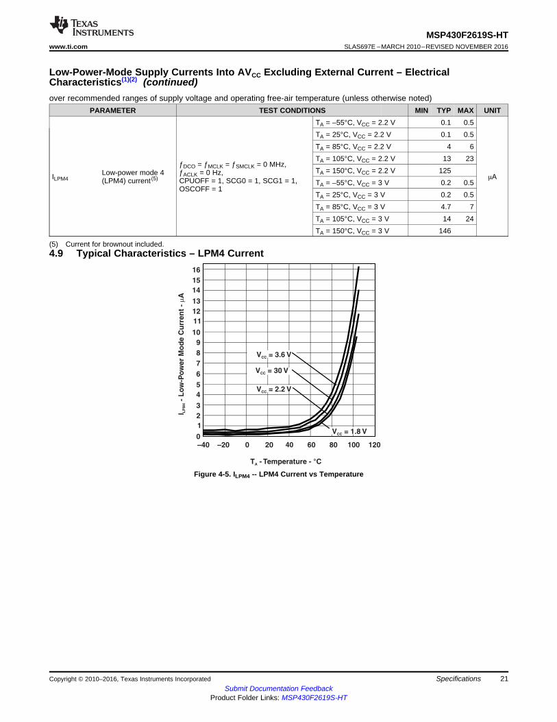
4.9 Typical Characteristics – LPM4 Current
Figure 4-5. ILPM4 -- LPM4 Current vs Temperature
22
MSP430F2619S-HTSLAS697E –MARCH 2010–REVISED NOVEMBER 2016 www.ti.com
Submit Documentation FeedbackProduct Folder Links: MSP430F2619S-HT
Specifications Copyright © 2010–2016, Texas Instruments Incorporated
(1) XIN and XT2IN in bypass mode only.
4.10 Schmitt-Trigger Inputs (Ports P1 Through P6, and RST/NMI, JTAG, XIN, andXT2IN) (1) – Electrical Characteristics
over recommended ranges of supply voltage and operating free-air temperature (unless otherwise noted)PARAMETER TEST CONDITIONS MIN TYP MAX UNIT
VIT+ Positive-going input threshold voltage0.45 x VCC 0.75 x VCC
VVCC = 2.2 V 1.00 1.65VCC = 3 V 1.35 2.25
VIT– Negative-going input threshold voltage0.25 x VCC 0.55 x VCC
VVCC = 2.2 V 0.55 1.20VCC = 3 V 0.75 1.65
Vhys Input voltage hysteresis (VIT+ – VIT–)VCC = 2.2 V 0.2 1
VVCC = 3 V 0.3 1
RPull Pullup/pulldown resistor For pullup: VIN = VSSFor pulldown: VIN = VCC
20 35 50 kΩ
CI Input capacitance VIN = VSS or VCC 5 pF
(1) An external signal sets the interrupt flag every time the minimum interrupt pulse width t(int) is met. It may be set even with trigger signalsshorter than t(int).
4.11 Inputs (Ports P1 and P2) – Electrical Characteristicsover recommended ranges of supply voltage and operating free-air temperature (unless otherwise noted)
PARAMETER TEST CONDITIONS MIN MAX UNIT
t(int) External interrupt timing Port P1, P2: P1.x to P2.x, External trigger pulsewidth to set interrupt flag (1), VCC = 2.2 V or 3 V 20 ns
(1) The leakage current is measured with VSS or VCC applied to the corresponding pin(s), unless otherwise noted.(2) The leakage of the digital port pins is measured individually. The port pin is selected for input and the pullup/pulldown resistor is
disabled.
4.12 Leakage Current (Ports P1 Through P6) – Electrical Characteristicsover recommended ranges of supply voltage and operating free-air temperature (unless otherwise noted)
PARAMETER TEST CONDITIONS MIN TYP MAX UNITIlkg(Px.x) High-impedance leakage current See (1) and (2), VCC = 2.2 V or 3 V ±250 nA
4.13 Standard Inputs - RST/NMI – Electrical Characteristicsover recommended ranges of supply voltage and operating free-air temperature (unless otherwise noted)
PARAMETER TEST CONDITIONS MIN MAX UNITVIL Low-level input voltage VCC = 2.2 V or 3 V VSS VSS + 0.6 VVIH High-level input voltage VCC = 2.2 V or 3 V 0.8 x VCC VCC V
23
MSP430F2619S-HTwww.ti.com SLAS697E –MARCH 2010–REVISED NOVEMBER 2016
Submit Documentation FeedbackProduct Folder Links: MSP430F2619S-HT
SpecificationsCopyright © 2010–2016, Texas Instruments Incorporated
(1) The maximum total current, IOH(max) and IOL(max), for all outputs combined, should not exceed ±12 mA to hold the maximum voltage dropspecified.
(2) The maximum total current, IOH(max) and IOL(max), for all outputs combined, should not exceed ±48 mA to hold the maximum voltage dropspecified.
4.14 Outputs (Ports P1 Through P6) – Electrical Characteristicsover recommended ranges of supply voltage and operating free-air temperature (unless otherwise noted)
PARAMETER TEST CONDITIONS MIN MAX UNIT
VOH High-level output voltage
IOH(max) = –1.5 mA (1), VCC = 2.2 V VCC – 0.25 VCC
VIOH(max) = –6 mA (2), VCC = 2.2 V VCC – 0.6 VCC
IOH(max) = –1.5 mA (1), VCC = 3 V VCC – 0.25 VCC
IOH(max) = –6 mA (2), VCC = 3 V VCC – 0.6 VCC
VOL Low-level output voltage
IOL(max) = 1.5 mA (1), VCC = 2.2 V VSS VSS+0.25
VIOL(max) = 6 mA (2), VCC = 2.2 V VSS VSS+0.6IOL(max) = 1.5 mA (1), VCC = 3 V VSS VSS+0.25IOL(max) = 6 mA (2), VCC = 3 V VSS VSS+0.6
(1) A resistive divider with 2 times 0.5 kΩ between VCC and VSS is used as load. The output is connected to the center tap of the divider.(2) The output voltage reaches at least 10% and 90% VCC at the specified toggle frequency.
4.15 Output Frequency (Ports P1 Through P6) – Electrical Characteristicsover recommended ranges of supply voltage and operating free-air temperature (unless otherwise noted)
PARAMETER TEST CONDITIONS MIN TYP MAX UNIT
ƒPx.yPort output frequency(with load) P1.4/SMCLK, CL = 20 pF, RL = 1 kΩ (1) (2) VCC = 2.2 V DC 10
MHzVCC = 3 V DC 12
ƒPort_CLKClock outputfrequency
P2.0/ACLK/CA2, P1.4/SMCLK,CL = 20 pF (2)
VCC = 2.2 V DC 12MHz
VCC = 3 V DC 16
t(Xdc)Duty cycle of outputfrequency
P5.6/ACLK, CL = 20 pF, LF mode 30% 50% 70%P5.6/ACLK, CL = 20 pF, XT1 mode 40% 50% 60%P5.4/MCLK, CL = 20 pF, XT1 mode 40% 60%
P5.4/MCLK, CL = 20 pF, DCO 50% – 15ns 50% 50% + 15
nsP1.4/SMCLK, CL = 20 pF, XT2 mode 40% 60%
P1.4/SMCLK, CL = 20 pF, DCO 50% – 15ns
50% + 15ns
VOH − High-Level Output Voltage − V
−25.0
−20.0
−15.0
−10.0
−5.0
0.0
0.0 0.5 1.0 1.5 2.0 2.5
TA = 25°C
TA = 85°C
OH
I−
Typ
ical
Hig
h-L
evel
Ou
tpu
t C
urr
en
t−
mA
VOH − High-Level Output Voltage − V
−50.0
−40.0
−30.0
−20.0
−10.0
0.0
0.0 0.5 1.0 1.5 2.0 2.5 3.0 3.5
TA = 25°C
TA = 85°C
OH
I−
Typ
ical
Hig
h-L
evel
Ou
tpu
t C
urr
en
t−
mA
VOL − Low-Level Output Voltage − V
0.0
5.0
10.0
15.0
20.0
25.0
0.0 0.5 1.0 1.5 2.0 2.5
TA = 25°C
TA = 85°C
OL
I−
Typ
ical
Lo
w-L
evel
Ou
tpu
t C
urr
en
t−
mA
VOL − Low-Level Output Voltage − V
0.0
10.0
20.0
30.0
40.0
50.0
0.0 0.5 1.0 1.5 2.0 2.5 3.0 3.5
TA = 25°C
TA = 85°C
OL
I−
Typ
ical
Lo
w-L
evel
Ou
tpu
t C
urr
en
t−
mA
24
MSP430F2619S-HTSLAS697E –MARCH 2010–REVISED NOVEMBER 2016 www.ti.com
Submit Documentation FeedbackProduct Folder Links: MSP430F2619S-HT
Specifications Copyright © 2010–2016, Texas Instruments Incorporated
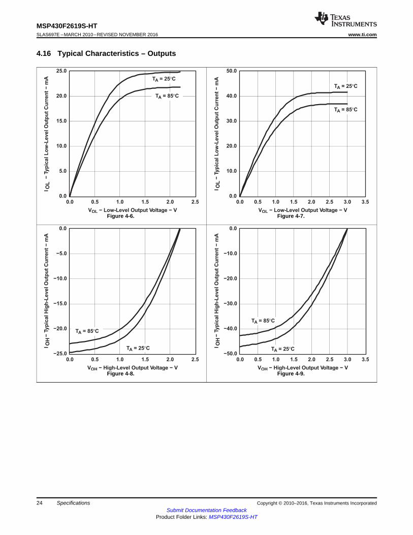
4.16 Typical Characteristics – Outputs
Figure 4-6. Figure 4-7.
Figure 4-8. Figure 4-9.
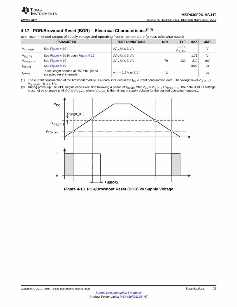
0
1
t d(BOR)
VCC
V(B_IT−)
Vhys(B_IT−)
VCC(start)
25
MSP430F2619S-HTwww.ti.com SLAS697E –MARCH 2010–REVISED NOVEMBER 2016
Submit Documentation FeedbackProduct Folder Links: MSP430F2619S-HT
SpecificationsCopyright © 2010–2016, Texas Instruments Incorporated
(1) The current consumption of the brownout module is already included in the ICC current consumption data. The voltage level V(B_IT–) +Vhys(B_IT– ) is ≤ 1.8 V.
(2) During power up, the CPU begins code execution following a period of td(BOR) after VCC = V(B_IT–) + Vhys(B_IT–). The default DCO settingsmust not be changed until VCC ≥ VCC(min), where VCC(min) is the minimum supply voltage for the desired operating frequency.
4.17 POR/Brownout Reset (BOR) – Electrical Characteristics (1) (2)
over recommended ranges of supply voltage and operating free-air temperature (unless otherwise noted)PARAMETER TEST CONDITIONS MIN TYP MAX UNIT
VCC(start) See Figure 4-10 dVCC/dt ≤ 3 V/s 0.7 ×V(B_IT–)
V
V(B_IT–) See Figure 4-10 through Figure 4-12 dVCC/dt ≤ 3 V/s 1.71 VVhys(B_IT–) See Figure 4-10 dVCC/dt ≤ 3 V/s 70 130 210 mVtd(BOR) See Figure 4-10 2000 μs
t(reset)Pulse length needed at RST/NMI pin toaccepted reset internally VCC = 2.2 V or 3 V 2 μs
Figure 4-10. POR/Brownout Reset (BOR) vs Supply Voltage
VCC
0
0.5
1
1.5
2
VCC(drop)
tpw
tpw − Pulse Width − ms
VC
C(d
rop
)−V
3 V
0.001 1 1000 tf tr
tpw − Pulse Width − ms
tf = tr
VCC(drop)
VCC
3 V
tpw
0
0.5
1
1.5
2
0.001 1 10001 ns 1 ns
tpw − Pulse Width − ms
VC
C(d
rop
)−
V
tpw − Pulse Width − ms
26
MSP430F2619S-HTSLAS697E –MARCH 2010–REVISED NOVEMBER 2016 www.ti.com
Submit Documentation FeedbackProduct Folder Links: MSP430F2619S-HT
Specifications Copyright © 2010–2016, Texas Instruments Incorporated
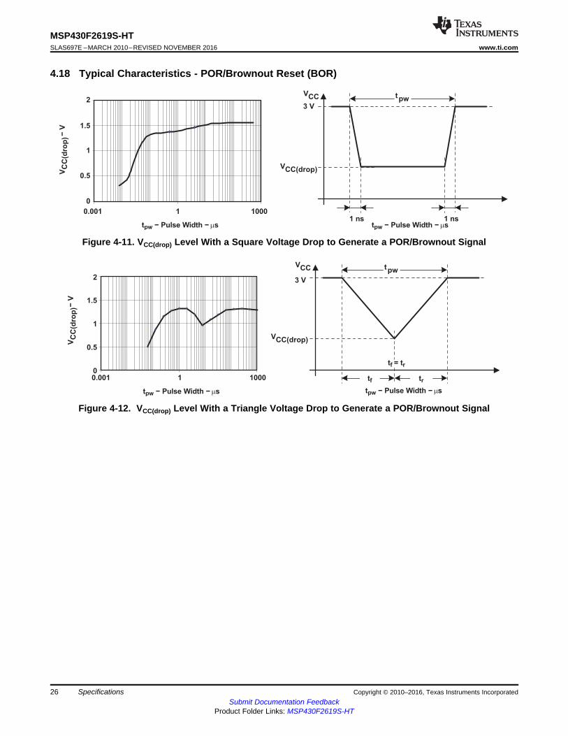
4.18 Typical Characteristics - POR/Brownout Reset (BOR)
Figure 4-11. VCC(drop) Level With a Square Voltage Drop to Generate a POR/Brownout Signal
Figure 4-12. VCC(drop) Level With a Triangle Voltage Drop to Generate a POR/Brownout Signal
27
MSP430F2619S-HTwww.ti.com SLAS697E –MARCH 2010–REVISED NOVEMBER 2016
Submit Documentation FeedbackProduct Folder Links: MSP430F2619S-HT
SpecificationsCopyright © 2010–2016, Texas Instruments Incorporated
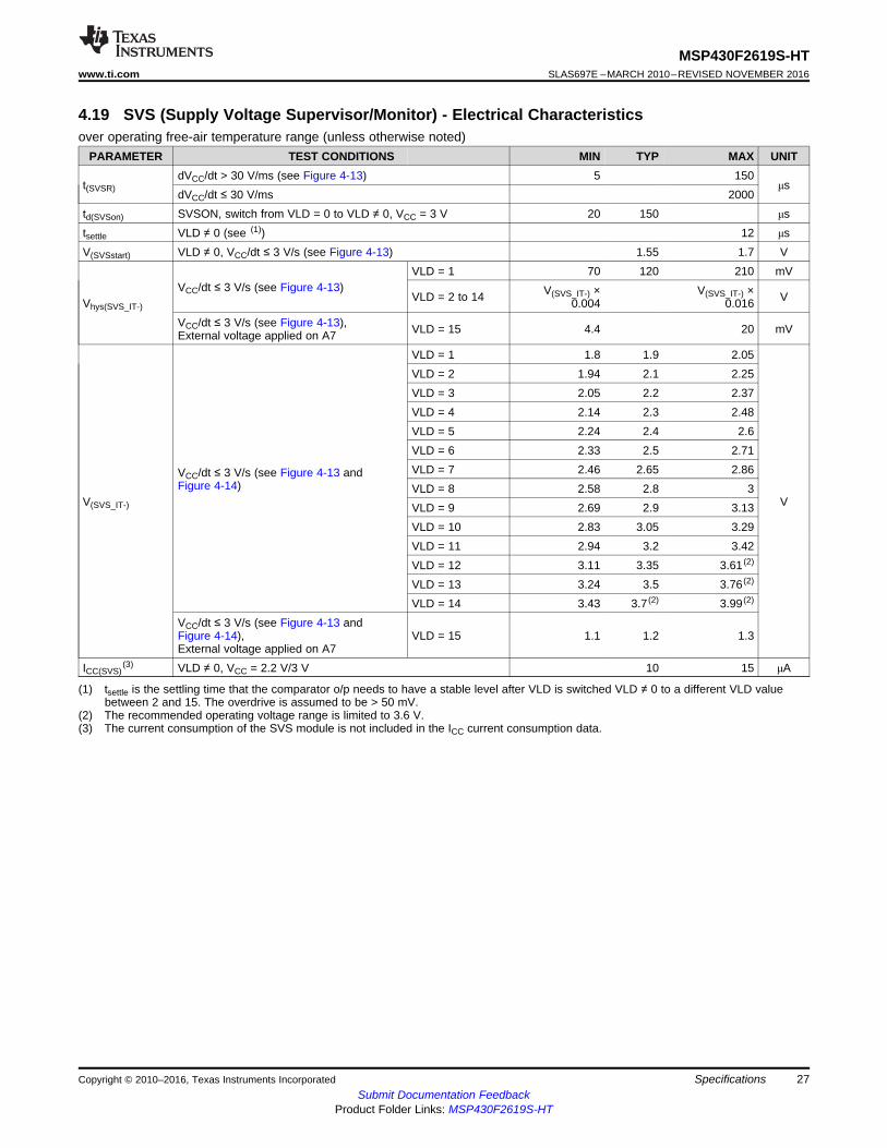
(1) tsettle is the settling time that the comparator o/p needs to have a stable level after VLD is switched VLD ≠ 0 to a different VLD valuebetween 2 and 15. The overdrive is assumed to be > 50 mV.
(2) The recommended operating voltage range is limited to 3.6 V.(3) The current consumption of the SVS module is not included in the ICC current consumption data.
4.19 SVS (Supply Voltage Supervisor/Monitor) - Electrical Characteristicsover operating free-air temperature range (unless otherwise noted)
PARAMETER TEST CONDITIONS MIN TYP MAX UNIT
t(SVSR)dVCC/dt > 30 V/ms (see Figure 4-13) 5 150
μsdVCC/dt ≤ 30 V/ms 2000
td(SVSon) SVSON, switch from VLD = 0 to VLD ≠ 0, VCC = 3 V 20 150 μstsettle VLD ≠ 0 (see (1)) 12 μsV(SVSstart) VLD ≠ 0, VCC/dt ≤ 3 V/s (see Figure 4-13) 1.55 1.7 V
Vhys(SVS_IT-)
VCC/dt ≤ 3 V/s (see Figure 4-13)VLD = 1 70 120 210 mV
VLD = 2 to 14 V(SVS_IT-) ×0.004
V(SVS_IT-) ×0.016 V
VCC/dt ≤ 3 V/s (see Figure 4-13),External voltage applied on A7 VLD = 15 4.4 20 mV
V(SVS_IT-)
VCC/dt ≤ 3 V/s (see Figure 4-13 andFigure 4-14)
VLD = 1 1.8 1.9 2.05
V
VLD = 2 1.94 2.1 2.25VLD = 3 2.05 2.2 2.37VLD = 4 2.14 2.3 2.48VLD = 5 2.24 2.4 2.6VLD = 6 2.33 2.5 2.71VLD = 7 2.46 2.65 2.86VLD = 8 2.58 2.8 3VLD = 9 2.69 2.9 3.13VLD = 10 2.83 3.05 3.29VLD = 11 2.94 3.2 3.42VLD = 12 3.11 3.35 3.61 (2)
VLD = 13 3.24 3.5 3.76 (2)
VLD = 14 3.43 3.7 (2) 3.99 (2)
VCC/dt ≤ 3 V/s (see Figure 4-13 andFigure 4-14),External voltage applied on A7
VLD = 15 1.1 1.2 1.3
ICC(SVS)(3) VLD ≠ 0, VCC = 2.2 V/3 V 10 15 μA
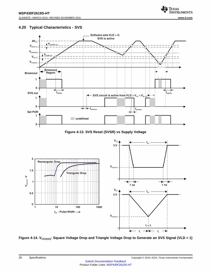
Rectangular Drop
Triangular Drop
V-V
CC
(min
)
t - Pulse Width - spw m
1 10 100 10000
0.5
1
1.5
2
VCC
3 V
VCC(min)
1 ns 1 ns
tpw
VCC
3 V
VCC(min)
tpw
tf
t = tf r
tr
Software sets VLD > 0:
SVS is activeAVCC
V(SVS_IT-)
V(SVSstart)
V(B_IT-)
VCC(start)
Brownout
1
0
SVS out
1
0
Set POR
1
0
Vhys(SVS_IT-)
Vhys(B_IT-)
Brownout
td(BOR)
Region
SVS circuit is active from VLD > V < VCC (B_IT-)
td(SVSon) td(SVSR)
td(BOR)
undefined
28
MSP430F2619S-HTSLAS697E –MARCH 2010–REVISED NOVEMBER 2016 www.ti.com
Submit Documentation FeedbackProduct Folder Links: MSP430F2619S-HT
Specifications Copyright © 2010–2016, Texas Instruments Incorporated
4.20 Typical Characteristics - SVS
Figure 4-13. SVS Reset (SVSR) vs Supply Voltage
Figure 4-14. VCC(min): Square Voltage Drop and Triangle Voltage Drop to Generate an SVS Signal (VLD = 1)
faverage 32 fDCO(RSEL,DCO) fDCO(RSEL,DCO 1)
MOD fDCO(RSEL,DCO) (32 MOD) fDCO(RSEL,DCO 1)
29
MSP430F2619S-HTwww.ti.com SLAS697E –MARCH 2010–REVISED NOVEMBER 2016
Submit Documentation FeedbackProduct Folder Links: MSP430F2619S-HT
SpecificationsCopyright © 2010–2016, Texas Instruments Incorporated
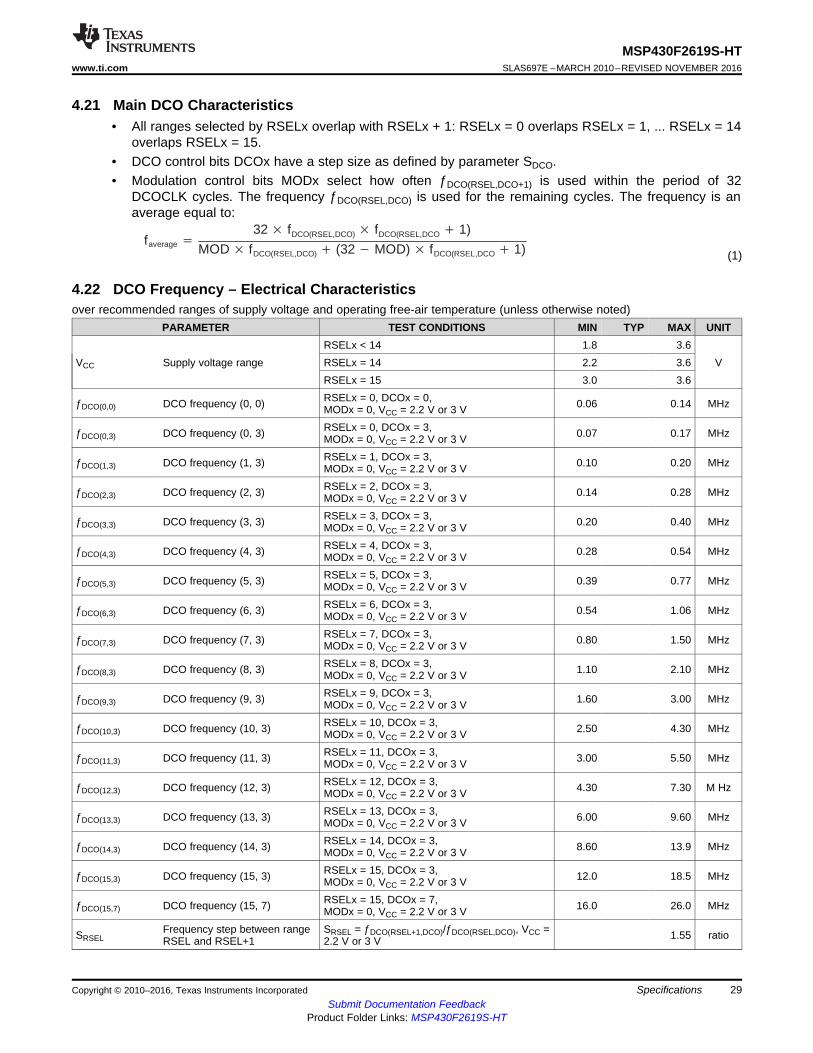
4.21 Main DCO Characteristics• All ranges selected by RSELx overlap with RSELx + 1: RSELx = 0 overlaps RSELx = 1, ... RSELx = 14
overlaps RSELx = 15.• DCO control bits DCOx have a step size as defined by parameter SDCO.• Modulation control bits MODx select how often ƒDCO(RSEL,DCO+1) is used within the period of 32
DCOCLK cycles. The frequency ƒDCO(RSEL,DCO) is used for the remaining cycles. The frequency is anaverage equal to:
(1)
4.22 DCO Frequency – Electrical Characteristicsover recommended ranges of supply voltage and operating free-air temperature (unless otherwise noted)
PARAMETER TEST CONDITIONS MIN TYP MAX UNIT
VCC Supply voltage rangeRSELx < 14 1.8 3.6
VRSELx = 14 2.2 3.6RSELx = 15 3.0 3.6
ƒDCO(0,0) DCO frequency (0, 0) RSELx = 0, DCOx = 0,MODx = 0, VCC = 2.2 V or 3 V 0.06 0.14 MHz
ƒDCO(0,3) DCO frequency (0, 3) RSELx = 0, DCOx = 3,MODx = 0, VCC = 2.2 V or 3 V 0.07 0.17 MHz
ƒDCO(1,3) DCO frequency (1, 3) RSELx = 1, DCOx = 3,MODx = 0, VCC = 2.2 V or 3 V 0.10 0.20 MHz
ƒDCO(2,3) DCO frequency (2, 3) RSELx = 2, DCOx = 3,MODx = 0, VCC = 2.2 V or 3 V 0.14 0.28 MHz
ƒDCO(3,3) DCO frequency (3, 3) RSELx = 3, DCOx = 3,MODx = 0, VCC = 2.2 V or 3 V 0.20 0.40 MHz
ƒDCO(4,3) DCO frequency (4, 3) RSELx = 4, DCOx = 3,MODx = 0, VCC = 2.2 V or 3 V 0.28 0.54 MHz
ƒDCO(5,3) DCO frequency (5, 3) RSELx = 5, DCOx = 3,MODx = 0, VCC = 2.2 V or 3 V 0.39 0.77 MHz
ƒDCO(6,3) DCO frequency (6, 3) RSELx = 6, DCOx = 3,MODx = 0, VCC = 2.2 V or 3 V 0.54 1.06 MHz
ƒDCO(7,3) DCO frequency (7, 3) RSELx = 7, DCOx = 3,MODx = 0, VCC = 2.2 V or 3 V 0.80 1.50 MHz
ƒDCO(8,3) DCO frequency (8, 3) RSELx = 8, DCOx = 3,MODx = 0, VCC = 2.2 V or 3 V 1.10 2.10 MHz
ƒDCO(9,3) DCO frequency (9, 3) RSELx = 9, DCOx = 3,MODx = 0, VCC = 2.2 V or 3 V 1.60 3.00 MHz
ƒDCO(10,3) DCO frequency (10, 3) RSELx = 10, DCOx = 3,MODx = 0, VCC = 2.2 V or 3 V 2.50 4.30 MHz
ƒDCO(11,3) DCO frequency (11, 3) RSELx = 11, DCOx = 3,MODx = 0, VCC = 2.2 V or 3 V 3.00 5.50 MHz
ƒDCO(12,3) DCO frequency (12, 3) RSELx = 12, DCOx = 3,MODx = 0, VCC = 2.2 V or 3 V 4.30 7.30 M Hz
ƒDCO(13,3) DCO frequency (13, 3) RSELx = 13, DCOx = 3,MODx = 0, VCC = 2.2 V or 3 V 6.00 9.60 MHz
ƒDCO(14,3) DCO frequency (14, 3) RSELx = 14, DCOx = 3,MODx = 0, VCC = 2.2 V or 3 V 8.60 13.9 MHz
ƒDCO(15,3) DCO frequency (15, 3) RSELx = 15, DCOx = 3,MODx = 0, VCC = 2.2 V or 3 V 12.0 18.5 MHz
ƒDCO(15,7) DCO frequency (15, 7) RSELx = 15, DCOx = 7,MODx = 0, VCC = 2.2 V or 3 V 16.0 26.0 MHz
SRSELFrequency step between rangeRSEL and RSEL+1
SRSEL = ƒDCO(RSEL+1,DCO)/ƒDCO(RSEL,DCO), VCC =2.2 V or 3 V 1.55 ratio
30
MSP430F2619S-HTSLAS697E –MARCH 2010–REVISED NOVEMBER 2016 www.ti.com
Submit Documentation FeedbackProduct Folder Links: MSP430F2619S-HT
Specifications Copyright © 2010–2016, Texas Instruments Incorporated
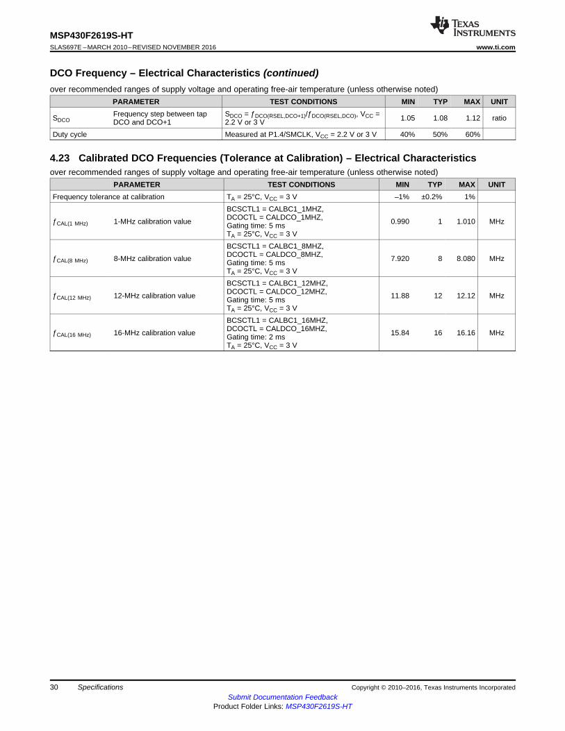
DCO Frequency – Electrical Characteristics (continued)over recommended ranges of supply voltage and operating free-air temperature (unless otherwise noted)
PARAMETER TEST CONDITIONS MIN TYP MAX UNIT
SDCOFrequency step between tapDCO and DCO+1
SDCO = ƒDCO(RSEL,DCO+1)/ƒDCO(RSEL,DCO), VCC =2.2 V or 3 V 1.05 1.08 1.12 ratio
Duty cycle Measured at P1.4/SMCLK, VCC = 2.2 V or 3 V 40% 50% 60%
4.23 Calibrated DCO Frequencies (Tolerance at Calibration) – Electrical Characteristicsover recommended ranges of supply voltage and operating free-air temperature (unless otherwise noted)
PARAMETER TEST CONDITIONS MIN TYP MAX UNITFrequency tolerance at calibration TA = 25°C, VCC = 3 V –1% ±0.2% 1%
ƒCAL(1 MHz) 1-MHz calibration value
BCSCTL1 = CALBC1_1MHZ,DCOCTL = CALDCO_1MHZ,Gating time: 5 msTA = 25°C, VCC = 3 V
0.990 1 1.010 MHz
ƒCAL(8 MHz) 8-MHz calibration value
BCSCTL1 = CALBC1_8MHZ,DCOCTL = CALDCO_8MHZ,Gating time: 5 msTA = 25°C, VCC = 3 V
7.920 8 8.080 MHz
ƒCAL(12 MHz) 12-MHz calibration value
BCSCTL1 = CALBC1_12MHZ,DCOCTL = CALDCO_12MHZ,Gating time: 5 msTA = 25°C, VCC = 3 V
11.88 12 12.12 MHz
ƒCAL(16 MHz) 16-MHz calibration value
BCSCTL1 = CALBC1_16MHZ,DCOCTL = CALDCO_16MHZ,Gating time: 2 msTA = 25°C, VCC = 3 V
15.84 16 16.16 MHz
31
MSP430F2619S-HTwww.ti.com SLAS697E –MARCH 2010–REVISED NOVEMBER 2016
Submit Documentation FeedbackProduct Folder Links: MSP430F2619S-HT
SpecificationsCopyright © 2010–2016, Texas Instruments Incorporated
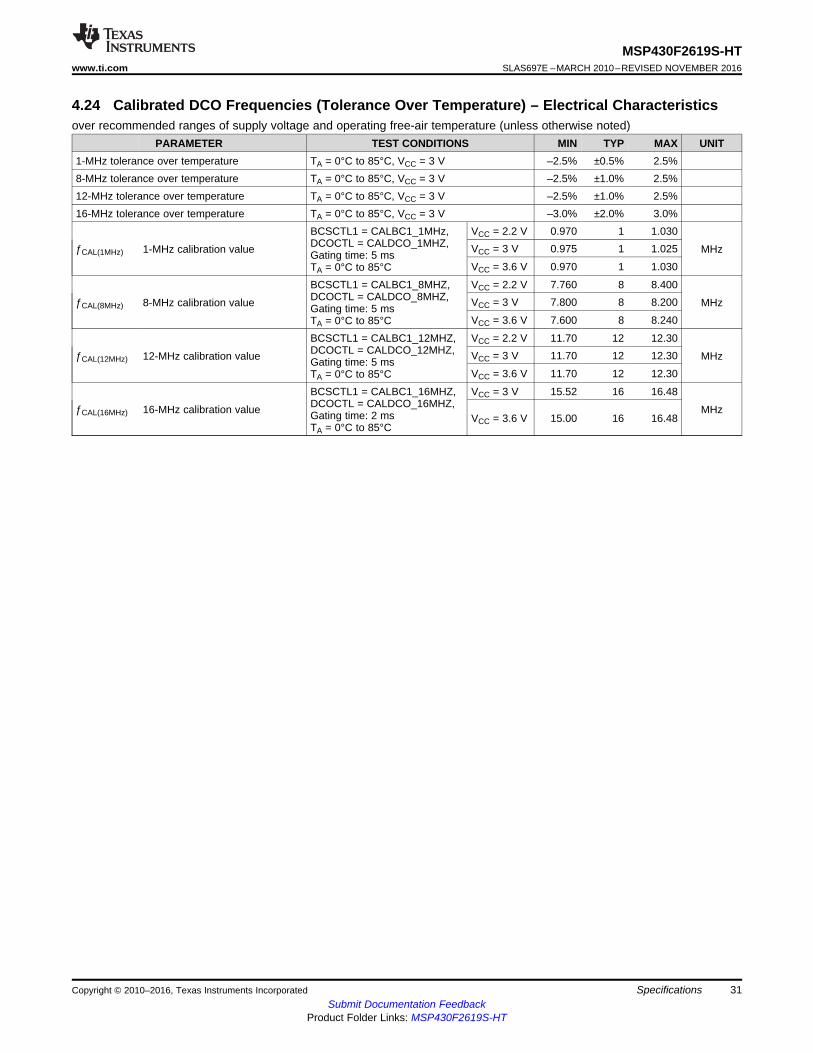
4.24 Calibrated DCO Frequencies (Tolerance Over Temperature) – Electrical Characteristicsover recommended ranges of supply voltage and operating free-air temperature (unless otherwise noted)
PARAMETER TEST CONDITIONS MIN TYP MAX UNIT1-MHz tolerance over temperature TA = 0°C to 85°C, VCC = 3 V –2.5% ±0.5% 2.5%8-MHz tolerance over temperature TA = 0°C to 85°C, VCC = 3 V –2.5% ±1.0% 2.5%12-MHz tolerance over temperature TA = 0°C to 85°C, VCC = 3 V –2.5% ±1.0% 2.5%16-MHz tolerance over temperature TA = 0°C to 85°C, VCC = 3 V –3.0% ±2.0% 3.0%
ƒCAL(1MHz) 1-MHz calibration value
BCSCTL1 = CALBC1_1MHz,DCOCTL = CALDCO_1MHZ,Gating time: 5 msTA = 0°C to 85°C
VCC = 2.2 V 0.970 1 1.030
MHzVCC = 3 V 0.975 1 1.025
VCC = 3.6 V 0.970 1 1.030
ƒCAL(8MHz) 8-MHz calibration value
BCSCTL1 = CALBC1_8MHZ,DCOCTL = CALDCO_8MHZ,Gating time: 5 msTA = 0°C to 85°C
VCC = 2.2 V 7.760 8 8.400
MHzVCC = 3 V 7.800 8 8.200
VCC = 3.6 V 7.600 8 8.240
ƒCAL(12MHz) 12-MHz calibration value
BCSCTL1 = CALBC1_12MHZ,DCOCTL = CALDCO_12MHZ,Gating time: 5 msTA = 0°C to 85°C
VCC = 2.2 V 11.70 12 12.30
MHzVCC = 3 V 11.70 12 12.30
VCC = 3.6 V 11.70 12 12.30
ƒCAL(16MHz) 16-MHz calibration value
BCSCTL1 = CALBC1_16MHZ,DCOCTL = CALDCO_16MHZ,Gating time: 2 msTA = 0°C to 85°C
VCC = 3 V 15.52 16 16.48
MHzVCC = 3.6 V 15.00 16 16.48
32
MSP430F2619S-HTSLAS697E –MARCH 2010–REVISED NOVEMBER 2016 www.ti.com
Submit Documentation FeedbackProduct Folder Links: MSP430F2619S-HT
Specifications Copyright © 2010–2016, Texas Instruments Incorporated
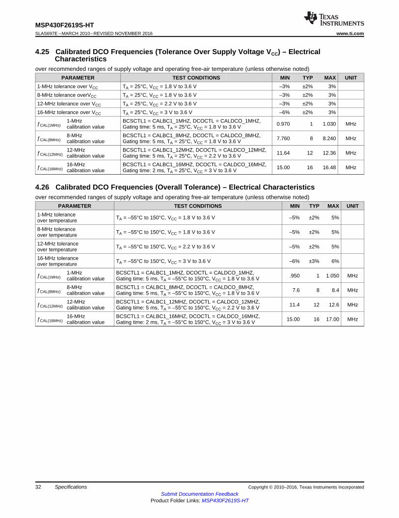
4.25 Calibrated DCO Frequencies (Tolerance Over Supply Voltage VCC) – ElectricalCharacteristics
over recommended ranges of supply voltage and operating free-air temperature (unless otherwise noted)PARAMETER TEST CONDITIONS MIN TYP MAX UNIT
1-MHz tolerance over VCC TA = 25°C, VCC = 1.8 V to 3.6 V –3% ±2% 3%8-MHz tolerance overVCC TA = 25°C, VCC = 1.8 V to 3.6 V –3% ±2% 3%12-MHz tolerance over VCC TA = 25°C, VCC = 2.2 V to 3.6 V –3% ±2% 3%16-MHz tolerance over VCC TA = 25°C, VCC = 3 V to 3.6 V –6% ±2% 3%
ƒCAL(1MHz)1-MHzcalibration value
BCSCTL1 = CALBC1_1MHZ, DCOCTL = CALDCO_1MHZ,Gating time: 5 ms, TA = 25°C, VCC = 1.8 V to 3.6 V 0.970 1 1.030 MHz
ƒCAL(8MHz)8-MHzcalibration value
BCSCTL1 = CALBC1_8MHZ, DCOCTL = CALDCO_8MHZ,Gating time: 5 ms, TA = 25°C, VCC = 1.8 V to 3.6 V 7.760 8 8.240 MHz
ƒCAL(12MHz)12-MHzcalibration value
BCSCTL1 = CALBC1_12MHZ, DCOCTL = CALDCO_12MHZ,Gating time: 5 ms, TA = 25°C, VCC = 2.2 V to 3.6 V 11.64 12 12.36 MHz
ƒCAL(16MHz)16-MHzcalibration value
BCSCTL1 = CALBC1_16MHZ, DCOCTL = CALDCO_16MHZ,Gating time: 2 ms, TA = 25°C, VCC = 3 V to 3.6 V 15.00 16 16.48 MHz
4.26 Calibrated DCO Frequencies (Overall Tolerance) – Electrical Characteristicsover recommended ranges of supply voltage and operating free-air temperature (unless otherwise noted)
PARAMETER TEST CONDITIONS MIN TYP MAX UNIT1-MHz toleranceover temperature TA = –55°C to 150°C, VCC = 1.8 V to 3.6 V –5% ±2% 5%
8-MHz toleranceover temperature TA = –55°C to 150°C, VCC = 1.8 V to 3.6 V –5% ±2% 5%
12-MHz toleranceover temperature TA = –55°C to 150°C, VCC = 2.2 V to 3.6 V –5% ±2% 5%
16-MHz toleranceover temperature TA = –55°C to 150°C, VCC = 3 V to 3.6 V –6% ±3% 6%
ƒCAL(1MHz)1-MHzcalibration value
BCSCTL1 = CALBC1_1MHZ, DCOCTL = CALDCO_1MHZ,Gating time: 5 ms, TA = –55°C to 150°C, VCC = 1.8 V to 3.6 V .950 1 1.050 MHz
ƒCAL(8MHz)8-MHzcalibration value
BCSCTL1 = CALBC1_8MHZ, DCOCTL = CALDCO_8MHZ,Gating time: 5 ms, TA = –55°C to 150°C, VCC = 1.8 V to 3.6 V 7.6 8 8.4 MHz
ƒCAL(12MHz)12-MHzcalibration value
BCSCTL1 = CALBC1_12MHZ, DCOCTL = CALDCO_12MHZ,Gating time: 5 ms, TA = –55°C to 150°C, VCC = 2.2 V to 3.6 V 11.4 12 12.6 MHz
ƒCAL(16MHz)16-MHzcalibration value
BCSCTL1 = CALBC1_16MHZ, DCOCTL = CALDCO_16MHZ,Gating time: 2 ms, TA = –55°C to 150°C, VCC = 3 V to 3.6 V 15.00 16 17.00 MHz
T = 105°CA
T = 85°CA
T = 25°CA
T = –40°CA
Fre
qu
en
cy -
MH
z
V - Supply Voltage - VCC
1.5 2 2.5 3 3.5 411.7
11.8
11.9
12
12.1
12.2
V - Supply Voltage - VCC
1.5 2 2.5 3 3.5 4
T = 105°CA
T = 85°CA
T = 25°CA
T = –40°CA
Fre
qu
en
cy -
MH
z
15.6
15.7
15.8
15.9
16
16.1
Fre
qu
en
cy
- M
Hz
V - Supply Voltage - VCC
T = 105°CA
T = 85°CA
T = 25°CA
T = –40°CA
1.5 2 2.5 3 3.5 40.98
0.99
1
1.01
1.02
V - Supply Voltage - VCC
1.5 2 2.5 3 3.5 4
Fre
qu
en
cy -
MH
z
T = 105°CA
T = 85°CA
T = 25°CA
T = –40°CA
7.80
7.85
7.90
7.95
8
8.05
8.10
8.15
8.20
33
MSP430F2619S-HTwww.ti.com SLAS697E –MARCH 2010–REVISED NOVEMBER 2016
Submit Documentation FeedbackProduct Folder Links: MSP430F2619S-HT
SpecificationsCopyright © 2010–2016, Texas Instruments Incorporated
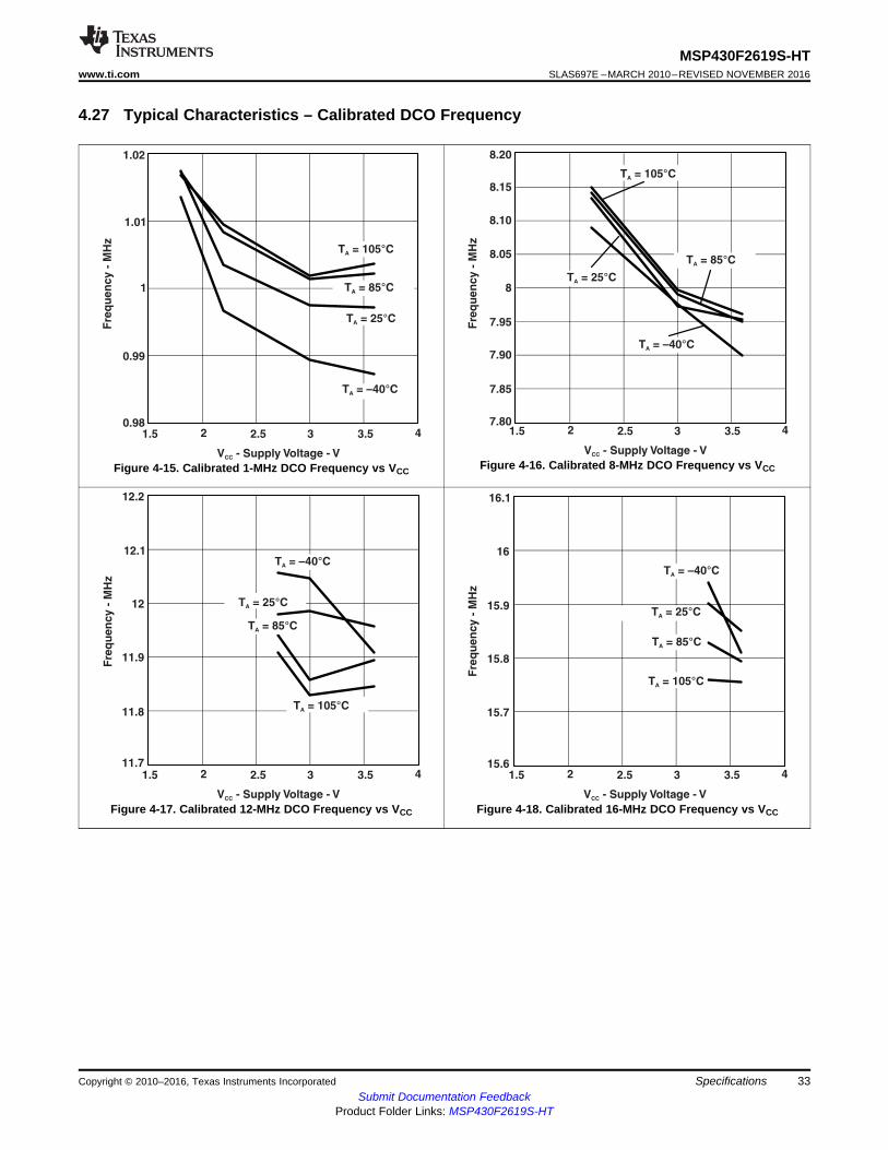
4.27 Typical Characteristics – Calibrated DCO Frequency
Figure 4-15. Calibrated 1-MHz DCO Frequency vs VCC Figure 4-16. Calibrated 8-MHz DCO Frequency vs VCC
Figure 4-17. Calibrated 12-MHz DCO Frequency vs VCC Figure 4-18. Calibrated 16-MHz DCO Frequency vs VCC
DCO Frequency − MHz
0.10
1.00
10.00
0.10 1.00 10.00
DC
O W
ake
Tim
e−
us
RSELx = 0...11RSELx = 12...15
34
MSP430F2619S-HTSLAS697E –MARCH 2010–REVISED NOVEMBER 2016 www.ti.com
Submit Documentation FeedbackProduct Folder Links: MSP430F2619S-HT
Specifications Copyright © 2010–2016, Texas Instruments Incorporated
(1) The DCO clock wake-up time is measured from the edge of an external wake-up signal (for example, port interrupt) to the first clockedge observable externally on a clock pin (MCLK or SMCLK).
(2) Parameter applicable only if DCOCLK is used for MCLK.
4.28 Wake-Up From Low-Power Modes (LPM3/4) – Electrical Characteristicsover recommended ranges of supply voltage and operating free-air temperature (unless otherwise noted)
PARAMETER TEST CONDITIONS MIN TYP MAX UNIT
tDCO,LPM3/4DCO clock wake-up timefrom LPM3/4 (1)
BCSCTL1 = CALBC1_1MHZ,DCOCTL = CALDCO_1MHZ,VCC = 2.2 V or 3 V
2
μs
BCSCTL1 = CALBC1_8MHZ,DCOCTL = CALDCO_8MHZ,VCC = 2.2 V or 3 V
1.5
BCSCTL1 = CALBC1_12MHZ,DCOCTL = CALDCO_12MHZ,VCC = 3 V
1
BCSCTL1 = CALBC1_16MHZ,DCOCTL = CALDCO_16MHZ,VCC = 3 V
1
tCPU,LPM3/4 CPU wake-up time from LPM3/4 (2) 1/ƒMCLK +tClock,LPM3/4
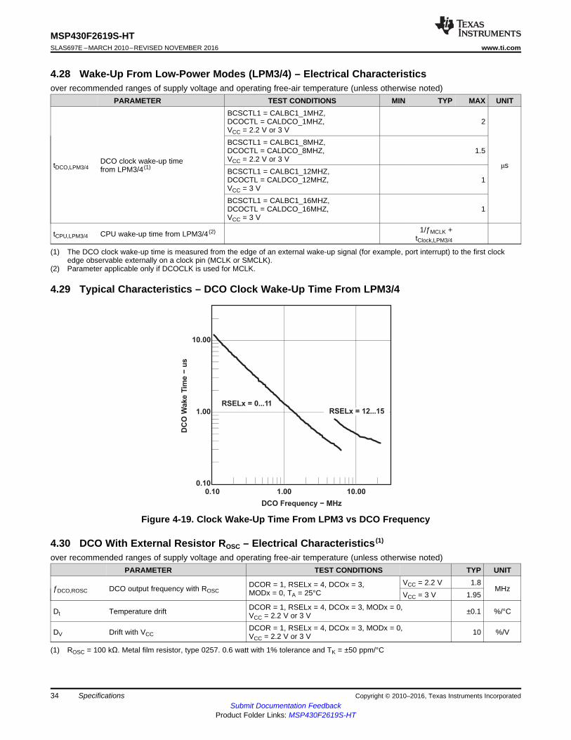
4.29 Typical Characteristics – DCO Clock Wake-Up Time From LPM3/4
Figure 4-19. Clock Wake-Up Time From LPM3 vs DCO Frequency
(1) ROSC = 100 kΩ. Metal film resistor, type 0257. 0.6 watt with 1% tolerance and TK = ±50 ppm/°C
4.30 DCO With External Resistor ROSC – Electrical Characteristics (1)
over recommended ranges of supply voltage and operating free-air temperature (unless otherwise noted)PARAMETER TEST CONDITIONS TYP UNIT
ƒDCO,ROSC DCO output frequency with ROSCDCOR = 1, RSELx = 4, DCOx = 3,MODx = 0, TA = 25°C
VCC = 2.2 V 1.8MHz
VCC = 3 V 1.95
Dt Temperature drift DCOR = 1, RSELx = 4, DCOx = 3, MODx = 0,VCC = 2.2 V or 3 V ±0.1 %/°C
DV Drift with VCCDCOR = 1, RSELx = 4, DCOx = 3, MODx = 0,VCC = 2.2 V or 3 V 10 %/V
0.000
0.200
0.400
0.600
0.800
1.000
1.200
1.400
1.600
1.800
2.000
-75 -25 25 75 125 175
DC
O F
req
ue
ncy
- M
Hz
T - Temperature - °CA
R = 100kOSC
R = 270kOSC
R = 1MOSC
0.01
0.10
1.00
10.00
10.00 100.00 1000.00 10000.00
ROSC − External Resistor − k
DC
O F
req
uen
cy
−M
Hz
RSELx = 4
0.01
0.10
1.00
10.00
10.00 100.00 1000.00 10000.00
ROSC − External Resistor − k
DC
O F
req
uen
cy
−M
Hz
RSELx = 4
35
MSP430F2619S-HTwww.ti.com SLAS697E –MARCH 2010–REVISED NOVEMBER 2016
Submit Documentation FeedbackProduct Folder Links: MSP430F2619S-HT
SpecificationsCopyright © 2010–2016, Texas Instruments Incorporated
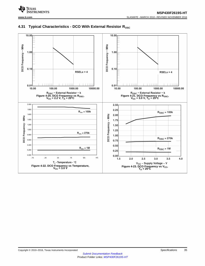
4.31 Typical Characteristics - DCO With External Resistor ROSC
Figure 4-20. DCO Frequency vs ROSC,VCC = 2.2 V, TA = 25°C
Figure 4-21. DCO Frequency vs ROSC,VCC = 3.0 V, TA = 25°C
Figure 4-22. DCO Frequency vs Temperature,VCC = 3.0 V Figure 4-23. DCO Frequency vs VCC,
TA = 25°C
36
MSP430F2619S-HTSLAS697E –MARCH 2010–REVISED NOVEMBER 2016 www.ti.com
Submit Documentation FeedbackProduct Folder Links: MSP430F2619S-HT
Specifications Copyright © 2010–2016, Texas Instruments Incorporated
(1) To improve EMI on the LFXT1 oscillator the following guidelines should be observed:• Keep as short of a trace as possible between the device and the crystal.• Design a good ground plane around the oscillator pins.• Prevent crosstalk from other clock or data lines into oscillator pins XIN and XOUT.• Avoid running PCB traces underneath or adjacent to the XIN and XOUT pins.• Use assembly materials and praxis to avoid any parasitic load on the oscillator XIN and XOUT pins.• If conformal coating is used, ensure that it does not induce capacitive/resistive leakage between the oscillator pins.• Do not route the XOUT line to the JTAG header to support the serial programming adapter as shown in other documentation. This
signal is no longer required for the serial programming adapter.(2) LFXT1 in 32-KHz mode is specified to function only between –55°C to 105°C. This module is know to fail above 110°C. For further info
contact TI support.(3) Includes parasitic bond and package capacitance (approximately 2 pF per pin). Since the PCB adds additional capacitance it is
recommended to verify the correct load by measuring the ACLK frequency. For a correct setup the effective load capacitance shouldalways match the specification of the used crystal.
(4) Frequencies below the MIN specification set the fault flag, frequencies above the MAX specification do not set the fault flag.Frequencies in between might set the flag.
(5) Measured with logic-level input frequency, but also applies to operation with crystals.
4.32 Crystal Oscillator (LFXT1) Low-Frequency Modes – Electrical Characteristics (1) (2)
over recommended ranges of supply voltage and operating free-air temperature (unless otherwise noted)PARAMETER TEST CONDITIONS MIN TYP MAX UNIT
ƒLFXT1,LFLFXT1 oscillator crystalfrequency, LF mode 0, 1 XTS = 0, LFXT1Sx = 0 or 1, VCC = 1.8 V to 3.6 V 32,768 Hz
ƒLFXT1,LF,logic
LFXT1 oscillator logic-level square-wave inputfrequency, LF mode
XTS = 0, LFXT1Sx = 3, VCC = 1.8 V to 3.6 V 10,000 32,768 50,000 Hz
OALFOscillation allowance forLF crystals
XTS = 0, LFXT1Sx = 0; ƒLFXT1,LF = 32,768 kHz,CL,eff = 6 pF 500
kΩXTS = 0, LFXT1Sx = 0;ƒLFXT1,LF = 32,768 kHz,CL,eff = 12 pF 200
CL,eff
Integrated effective loadcapacitance,LF mode (3)
XTS = 0
XCAPx = 0 1
pFXCAPx = 1 5.5XCAPx = 2 8.5XCAPx = 3 11
Duty cycle LF mode XTS = 0, Measured at P1.4/ACLK,ƒLFXT1,LF = 32,768 Hz, VCC = 2.2 V or 3 V 30% 50% 70%
ƒFault,LFOscillator fault frequencythreshold, LF mode (4) XTS = 0, LFXT1Sx = 3 (5), VCC = 2.2 V or 3 V 10 10,000 Hz
(1) Calculated using the box method:S Version: (MAX(–55 to 150°C) – MIN(–55 to 150°C))/MIN(–55 to 150°C)/(150°C – (–55°C))
(2) Calculated using the box method: (MAX(1.8 V to 3.6 V) – MIN(1.8V to 3.6 V))/MIN(1.8 V to 3.6 V)/(3.6 V – 1.8 V)
4.33 Internal Very-Low-Power, Low-Frequency Oscillator (VLO) – Electrical Characteristicsover recommended ranges of supply voltage and operating free-air temperature (unless otherwise noted)
PARAMETER TEST CONDITIONS MIN TYP MAX UNIT
ƒVLO VLO frequencyTA = –55°C to 85°C, VCC = 2.2 V or 3 V 4 12 20
kHzTA = 150°C, VCC = 2.2 V or 3 V 22
dƒVLO/dT VLO frequency temperature drift See (1), VCC = 2.2 V or 3 V 0.5 0.8 %/°CdƒVLO/dVCC VLO frequency supply voltage drift See (2), TA = 25°C, VCC = 1.8 V to 3.6V 4 %/V
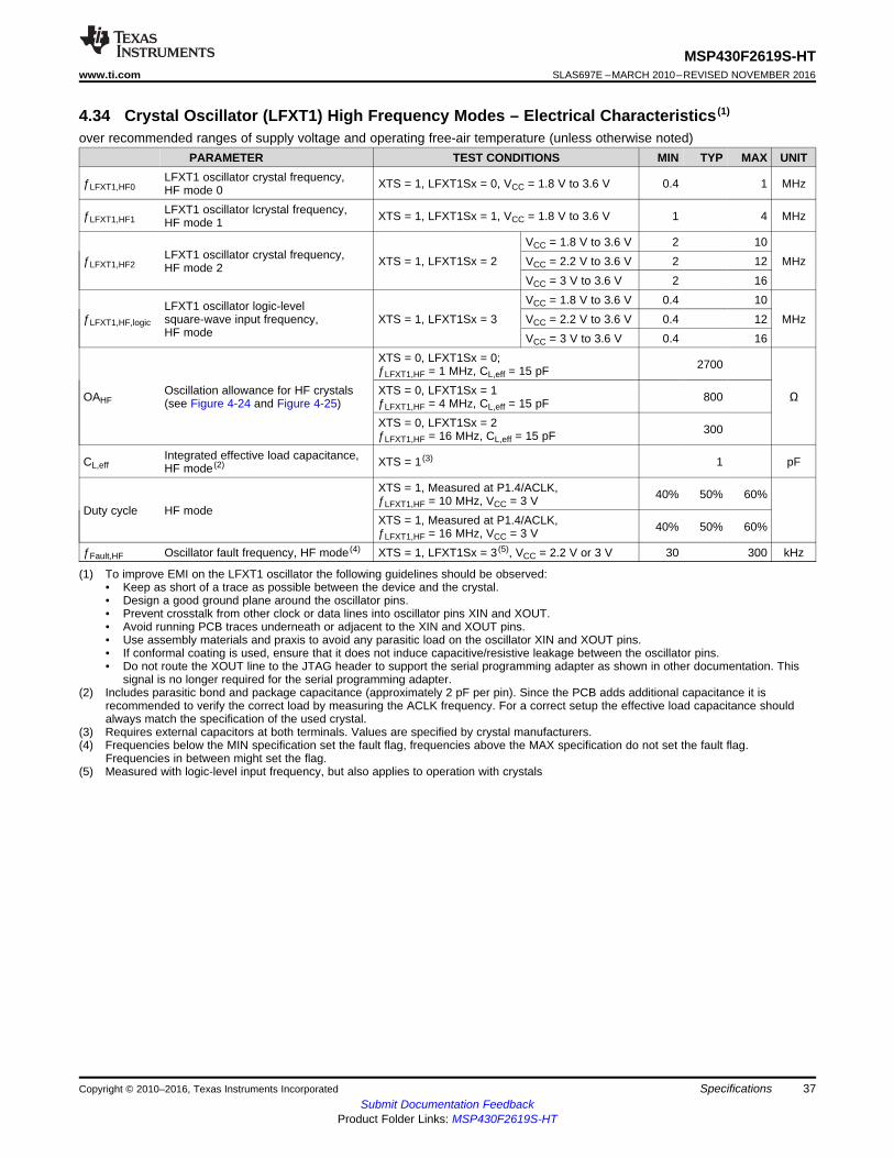
37
MSP430F2619S-HTwww.ti.com SLAS697E –MARCH 2010–REVISED NOVEMBER 2016
Submit Documentation FeedbackProduct Folder Links: MSP430F2619S-HT
SpecificationsCopyright © 2010–2016, Texas Instruments Incorporated
(1) To improve EMI on the LFXT1 oscillator the following guidelines should be observed:• Keep as short of a trace as possible between the device and the crystal.• Design a good ground plane around the oscillator pins.• Prevent crosstalk from other clock or data lines into oscillator pins XIN and XOUT.• Avoid running PCB traces underneath or adjacent to the XIN and XOUT pins.• Use assembly materials and praxis to avoid any parasitic load on the oscillator XIN and XOUT pins.• If conformal coating is used, ensure that it does not induce capacitive/resistive leakage between the oscillator pins.• Do not route the XOUT line to the JTAG header to support the serial programming adapter as shown in other documentation. This
signal is no longer required for the serial programming adapter.(2) Includes parasitic bond and package capacitance (approximately 2 pF per pin). Since the PCB adds additional capacitance it is
recommended to verify the correct load by measuring the ACLK frequency. For a correct setup the effective load capacitance shouldalways match the specification of the used crystal.
(3) Requires external capacitors at both terminals. Values are specified by crystal manufacturers.(4) Frequencies below the MIN specification set the fault flag, frequencies above the MAX specification do not set the fault flag.
Frequencies in between might set the flag.(5) Measured with logic-level input frequency, but also applies to operation with crystals
4.34 Crystal Oscillator (LFXT1) High Frequency Modes – Electrical Characteristics (1)
over recommended ranges of supply voltage and operating free-air temperature (unless otherwise noted)PARAMETER TEST CONDITIONS MIN TYP MAX UNIT
ƒLFXT1,HF0LFXT1 oscillator crystal frequency,HF mode 0 XTS = 1, LFXT1Sx = 0, VCC = 1.8 V to 3.6 V 0.4 1 MHz
ƒLFXT1,HF1LFXT1 oscillator lcrystal frequency,HF mode 1 XTS = 1, LFXT1Sx = 1, VCC = 1.8 V to 3.6 V 1 4 MHz
ƒLFXT1,HF2LFXT1 oscillator crystal frequency,HF mode 2 XTS = 1, LFXT1Sx = 2
VCC = 1.8 V to 3.6 V 2 10MHzVCC = 2.2 V to 3.6 V 2 12
VCC = 3 V to 3.6 V 2 16
ƒLFXT1,HF,logic
LFXT1 oscillator logic-levelsquare-wave input frequency,HF mode
XTS = 1, LFXT1Sx = 3VCC = 1.8 V to 3.6 V 0.4 10
MHzVCC = 2.2 V to 3.6 V 0.4 12VCC = 3 V to 3.6 V 0.4 16
OAHFOscillation allowance for HF crystals(see Figure 4-24 and Figure 4-25)
XTS = 0, LFXT1Sx = 0;ƒLFXT1,HF = 1 MHz, CL,eff = 15 pF 2700
ΩXTS = 0, LFXT1Sx = 1ƒLFXT1,HF = 4 MHz, CL,eff = 15 pF 800
XTS = 0, LFXT1Sx = 2ƒLFXT1,HF = 16 MHz, CL,eff = 15 pF 300
CL,effIntegrated effective load capacitance,HF mode (2) XTS = 1 (3) 1 pF
Duty cycle HF mode
XTS = 1, Measured at P1.4/ACLK,ƒLFXT1,HF = 10 MHz, VCC = 3 V 40% 50% 60%
XTS = 1, Measured at P1.4/ACLK,ƒLFXT1,HF = 16 MHz, VCC = 3 V 40% 50% 60%
ƒFault,HF Oscillator fault frequency, HF mode (4) XTS = 1, LFXT1Sx = 3 (5), VCC = 2.2 V or 3 V 30 300 kHz
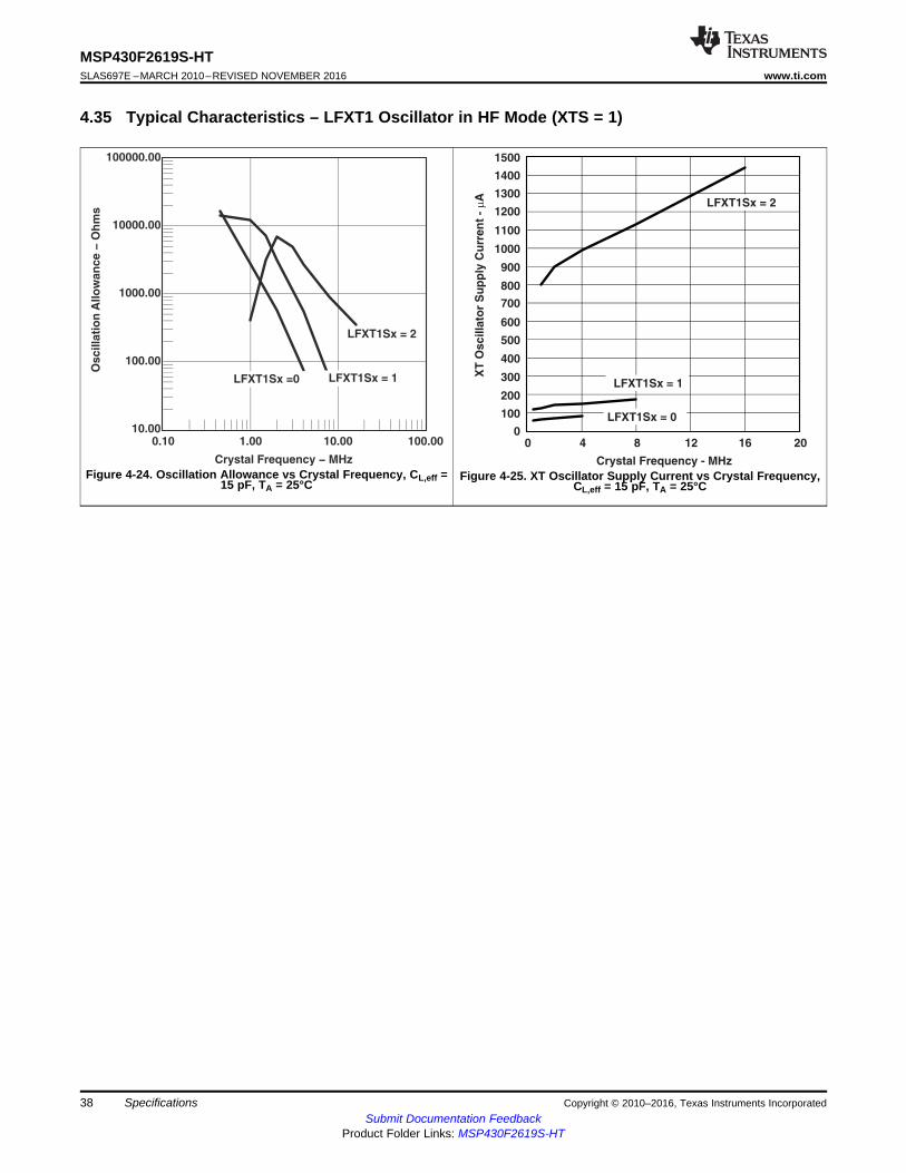
LFXT1Sx = 0
LFXT1Sx = 1
LFXT1Sx = 2
Crystal Frequency - MHz
XT
Os
cil
lato
r S
up
ply
Cu
rre
nt
-A
m
0 4 8 12 16 200
100
200
300
400
500
600
700
800
900
1000
1100
1200
1300
1400
1500
38
MSP430F2619S-HTSLAS697E –MARCH 2010–REVISED NOVEMBER 2016 www.ti.com
Submit Documentation FeedbackProduct Folder Links: MSP430F2619S-HT
Specifications Copyright © 2010–2016, Texas Instruments Incorporated
4.35 Typical Characteristics – LFXT1 Oscillator in HF Mode (XTS = 1)
Figure 4-24. Oscillation Allowance vs Crystal Frequency, CL,eff =15 pF, TA = 25°C
Figure 4-25. XT Oscillator Supply Current vs Crystal Frequency,CL,eff = 15 pF, TA = 25°C
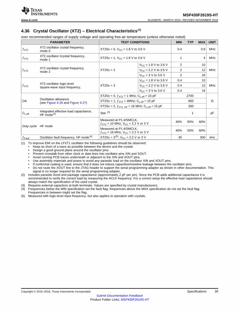
39
MSP430F2619S-HTwww.ti.com SLAS697E –MARCH 2010–REVISED NOVEMBER 2016
Submit Documentation FeedbackProduct Folder Links: MSP430F2619S-HT
SpecificationsCopyright © 2010–2016, Texas Instruments Incorporated
(1) To improve EMI on the LFXT1 oscillator the following guidelines should be observed:• Keep as short of a trace as possible between the device and the crystal.• Design a good ground plane around the oscillator pins.• Prevent crosstalk from other clock or data lines into oscillator pins XIN and XOUT.• Avoid running PCB traces underneath or adjacent to the XIN and XOUT pins.• Use assembly materials and praxis to avoid any parasitic load on the oscillator XIN and XOUT pins.• If conformal coating is used, ensure that it does not induce capacitive/resistive leakage between the oscillator pins.• Do not route the XOUT line to the JTAG header to support the serial programming adapter as shown in other documentation. This
signal is no longer required for the serial programming adapter.(2) Includes parasitic bond and package capacitance (approximately 2 pF per pin). Since the PCB adds additional capacitance it is
recommended to verify the correct load by measuring the ACLK frequency. For a correct setup the effective load capacitance shouldalways match the specification of the used crystal.
(3) Requires external capacitors at both terminals. Values are specified by crystal manufacturers.(4) Frequencies below the MIN specification set the fault flag, frequencies above the MAX specification do not set the fault flag.
Frequencies in between might set the flag.(5) Measured with logic-level input frequency, but also applies to operation with crystals.
4.36 Crystal Oscillator (XT2) – Electrical Characteristics (1)
over recommended ranges of supply voltage and operating free-air temperature (unless otherwise noted)PARAMETER TEST CONDITIONS MIN TYP MAX UNIT
ƒXT2XT2 oscillator crystal frequency,mode 0 XT2Sx = 0, VCC = 1.8 V to 3.6 V 0.4 0.9 MHz
ƒXT2XT2 oscillator lcrystal frequency,mode 1 XT2Sx = 1, VCC = 1.8 V to 3.6 V 1 4 MHz
ƒXT2XT2 oscillator crystal frequency,mode 2 XT2Sx = 2
VCC = 1.8 V to 3.6 V 2 10MHzVCC = 2.2 V to 3.6 V 2 12
VCC = 3 V to 3.6 V 2 16
ƒXT2XT2 oscillator logic-levelsquare-wave input frequency, XT2Sx = 3
VCC = 1.8 V to 3.6 V 0.4 10MHzVCC = 2.2 V to 3.6 V 0.4 12
VCC = 3 V to 3.6 V 0.4 16
OA Oscillation allowance(see Figure 4-26 and Figure 4-27)
XT2Sx = 0, ƒXT2 = 1 MHz; CL,eff = 15 pF 2700ΩXT2Sx = 1, ƒXT2 = 4MHz; CL,eff = 15 pF 800
XT2Sx = 2, ƒXT1, HF = 16 MHz; CL,eff = 15 pF 300
CL,effIntegrated effective load capacitance,HF mode (2) See (3) 1 pF
Duty cycle HF mode
Measured at P1.4/SMCLK,ƒXT2 = 10 MHz, VCC = 2.2 V or 3 V 40% 50% 60%
Measured at P1.4/SMCLK,ƒXT2 = 16 MHz, VCC = 2.2 V or 3 V 40% 50% 60%
ƒFault Oscillator fault frequency, HF mode (4) XT2Sx = 3 (5), VCC = 2.2 V or 3 V 30 300 kHz
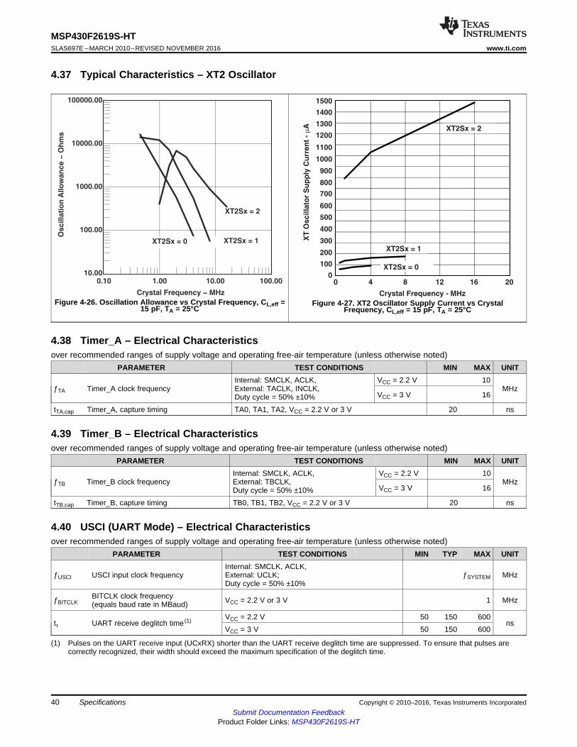
XT
Oscilla
tor
Su
pp
ly C
urr
en
t -
Am
0
100
200
300
400
500
600
700
800
900
1000
1100
1200
1300
1400
1500
Crystal Frequency - MHz
0 4 8 12 16 20
XT2Sx = 0
XT2Sx = 1
XT2Sx = 2
40
MSP430F2619S-HTSLAS697E –MARCH 2010–REVISED NOVEMBER 2016 www.ti.com
Submit Documentation FeedbackProduct Folder Links: MSP430F2619S-HT
Specifications Copyright © 2010–2016, Texas Instruments Incorporated
4.37 Typical Characteristics – XT2 Oscillator
Figure 4-26. Oscillation Allowance vs Crystal Frequency, CL,eff =15 pF, TA = 25°C
Figure 4-27. XT2 Oscillator Supply Current vs CrystalFrequency, CL,eff = 15 pF, TA = 25°C
4.38 Timer_A – Electrical Characteristicsover recommended ranges of supply voltage and operating free-air temperature (unless otherwise noted)
PARAMETER TEST CONDITIONS MIN MAX UNIT
ƒTA Timer_A clock frequencyInternal: SMCLK, ACLK,External: TACLK, INCLK,Duty cycle = 50% ±10%
VCC = 2.2 V 10MHz
VCC = 3 V 16
tTA,cap Timer_A, capture timing TA0, TA1, TA2, VCC = 2.2 V or 3 V 20 ns
4.39 Timer_B – Electrical Characteristicsover recommended ranges of supply voltage and operating free-air temperature (unless otherwise noted)
PARAMETER TEST CONDITIONS MIN MAX UNIT
ƒTB Timer_B clock frequencyInternal: SMCLK, ACLK,External: TBCLK,Duty cycle = 50% ±10%
VCC = 2.2 V 10MHz
VCC = 3 V 16
tTB,cap Timer_B, capture timing TB0, TB1, TB2, VCC = 2.2 V or 3 V 20 ns
(1) Pulses on the UART receive input (UCxRX) shorter than the UART receive deglitch time are suppressed. To ensure that pulses arecorrectly recognized, their width should exceed the maximum specification of the deglitch time.
4.40 USCI (UART Mode) – Electrical Characteristicsover recommended ranges of supply voltage and operating free-air temperature (unless otherwise noted)
PARAMETER TEST CONDITIONS MIN TYP MAX UNIT
ƒUSCI USCI input clock frequencyInternal: SMCLK, ACLK,External: UCLK;Duty cycle = 50% ±10%
ƒSYSTEM MHz
ƒBITCLKBITCLK clock frequency(equals baud rate in MBaud) VCC = 2.2 V or 3 V 1 MHz
tτ UART receive deglitch time (1) VCC = 2.2 V 50 150 600ns
VCC = 3 V 50 150 600
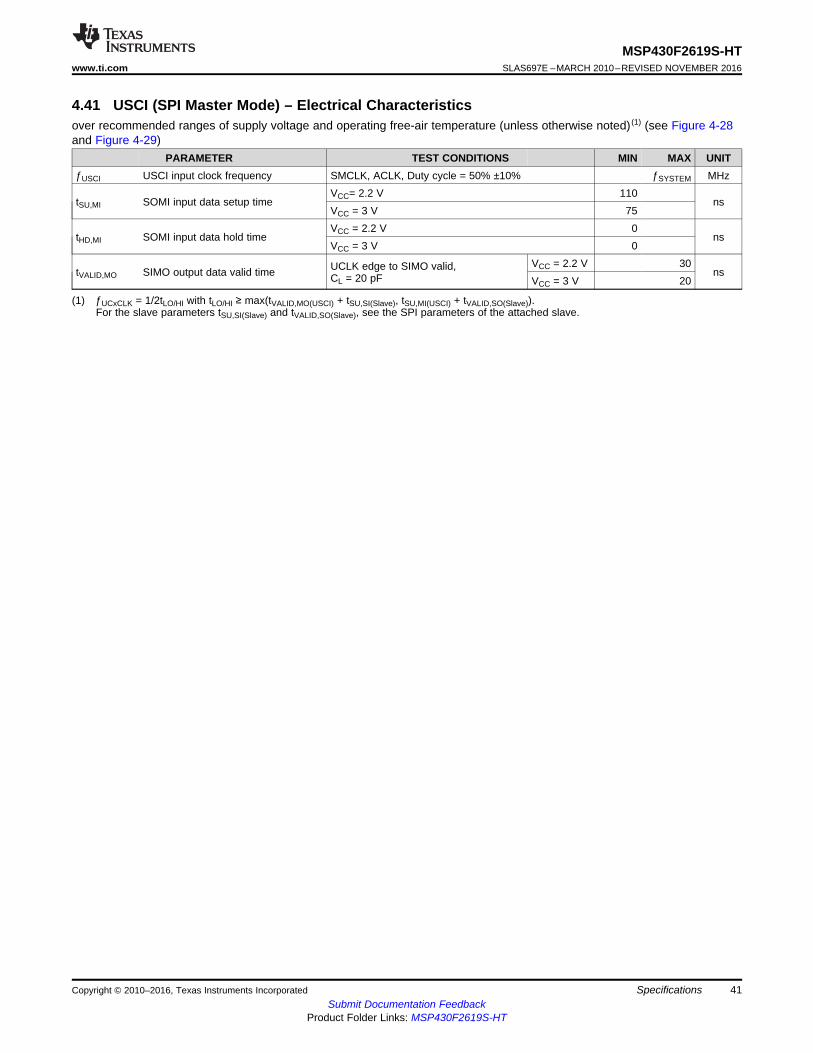
41
MSP430F2619S-HTwww.ti.com SLAS697E –MARCH 2010–REVISED NOVEMBER 2016
Submit Documentation FeedbackProduct Folder Links: MSP430F2619S-HT
SpecificationsCopyright © 2010–2016, Texas Instruments Incorporated
(1) ƒUCxCLK = 1/2tLO/HI with tLO/HI ≥ max(tVALID,MO(USCI) + tSU,SI(Slave), tSU,MI(USCI) + tVALID,SO(Slave)).For the slave parameters tSU,SI(Slave) and tVALID,SO(Slave), see the SPI parameters of the attached slave.
4.41 USCI (SPI Master Mode) – Electrical Characteristicsover recommended ranges of supply voltage and operating free-air temperature (unless otherwise noted) (1) (see Figure 4-28and Figure 4-29)
PARAMETER TEST CONDITIONS MIN MAX UNITƒUSCI USCI input clock frequency SMCLK, ACLK, Duty cycle = 50% ±10% ƒSYSTEM MHz
tSU,MI SOMI input data setup timeVCC= 2.2 V 110
nsVCC = 3 V 75
tHD,MI SOMI input data hold timeVCC = 2.2 V 0
nsVCC = 3 V 0
tVALID,MO SIMO output data valid time UCLK edge to SIMO valid,CL = 20 pF
VCC = 2.2 V 30ns
VCC = 3 V 20
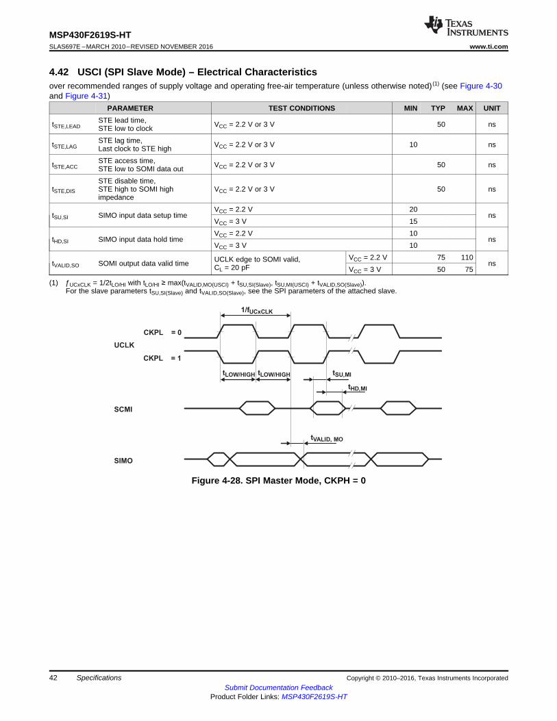
UCLK
SCMI
SIMO
CKPL = 0
CKPL = 1
1/fUCxCLK
tLOW/HIGH tLOW/HIGH tSU,MI
tHD,MI
tVALID, MO
42
MSP430F2619S-HTSLAS697E –MARCH 2010–REVISED NOVEMBER 2016 www.ti.com
Submit Documentation FeedbackProduct Folder Links: MSP430F2619S-HT
Specifications Copyright © 2010–2016, Texas Instruments Incorporated
(1) ƒUCxCLK = 1/2tLO/HI with tLO/HI ≥ max(tVALID,MO(USCI) + tSU,SI(Slave), tSU,MI(USCI) + tVALID,SO(Slave)).For the slave parameters tSU,SI(Slave) and tVALID,SO(Slave), see the SPI parameters of the attached slave.
4.42 USCI (SPI Slave Mode) – Electrical Characteristicsover recommended ranges of supply voltage and operating free-air temperature (unless otherwise noted) (1) (see Figure 4-30and Figure 4-31)
PARAMETER TEST CONDITIONS MIN TYP MAX UNIT
tSTE,LEADSTE lead time,STE low to clock VCC = 2.2 V or 3 V 50 ns
tSTE,LAGSTE lag time,Last clock to STE high VCC = 2.2 V or 3 V 10 ns
tSTE,ACCSTE access time,STE low to SOMI data out VCC = 2.2 V or 3 V 50 ns
tSTE,DIS
STE disable time,STE high to SOMI highimpedance
VCC = 2.2 V or 3 V 50 ns
tSU,SI SIMO input data setup timeVCC = 2.2 V 20
nsVCC = 3 V 15
tHD,SI SIMO input data hold timeVCC = 2.2 V 10
nsVCC = 3 V 10
tVALID,SO SOMI output data valid time UCLK edge to SOMI valid,CL = 20 pF
VCC = 2.2 V 75 110ns
VCC = 3 V 50 75
Figure 4-28. SPI Master Mode, CKPH = 0
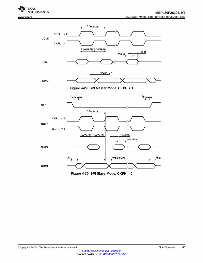
STE
UCLK
SIMO
SOMI
CKPL = 0
CKPL = 1
1/fUCxCLK
tSTE,LEAD
tLOW,HIGH tLOW,HIGH
tACC
tSTE,LAG
tSU,SIMO
tHD,SIMO
tVALID,SOMI tDIS
UCLK
SCMI
SIMO
CKPL = 0
CKPL = 1
1/fUCxCLK
tLOW/HIGH tLOW/HIGH
tSU,MI
tHD,MI
tVALID, MO
43
MSP430F2619S-HTwww.ti.com SLAS697E –MARCH 2010–REVISED NOVEMBER 2016
Submit Documentation FeedbackProduct Folder Links: MSP430F2619S-HT
SpecificationsCopyright © 2010–2016, Texas Instruments Incorporated
Figure 4-29. SPI Master Mode, CKPH = 1
Figure 4-30. SPI Slave Mode, CKPH = 0
,
STE
UCLK
SIMO
SOMI
CKPL = 0
CKPL = 1
1/fUCxCLK
tSTE,LEAD
tLOW,HIGH tLOW,HIGH
tACC
tSTE,LAG
tDIS
tSU,SI
tVALID,SO
tHD,SI
44
MSP430F2619S-HTSLAS697E –MARCH 2010–REVISED NOVEMBER 2016 www.ti.com
Submit Documentation FeedbackProduct Folder Links: MSP430F2619S-HT
Specifications Copyright © 2010–2016, Texas Instruments Incorporated
Figure 4-31. SPI Slave Mode, CKPH = 1
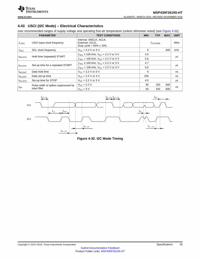
SDA
SCL
tLOW
tHD ,DAT
tSU ,DAT
tHD ,STA tSU ,STA tHD ,STA
tHIGH
tSU , STO
tSP
tBUF
45
MSP430F2619S-HTwww.ti.com SLAS697E –MARCH 2010–REVISED NOVEMBER 2016
Submit Documentation FeedbackProduct Folder Links: MSP430F2619S-HT
SpecificationsCopyright © 2010–2016, Texas Instruments Incorporated
4.43 USCI (I2C Mode) – Electrical Characteristicsover recommended ranges of supply voltage and operating free-air temperature (unless otherwise noted) (see Figure 4-32)
PARAMETER TEST CONDITIONS MIN TYP MAX UNIT
ƒUSCI USCI input clock frequencyInternal: SMCLK, ACLK,External: UCLK,Duty cycle = 50% ± 10%
ƒSYSTEM MHz
ƒSCL SCL clock frequency VCC = 2.2 V or 3 V 0 400 kHz
tHD,STA Hold time (repeated) STARTƒSCL ≤ 100 kHz, VCC = 2.2 V or 3 V 4.0
μsƒSCL > 100 kHz, VCC = 2.2 V or 3 V 0.6
tSU,STA Set-up time for a repeated STARTƒSCL ≤ 100 kHz, VCC = 2.2 V or 3 V 4.7
μsƒSCL > 100 kHz, VCC = 2.2 V or 3 V 0.6
tHD,DAT Data hold time VCC = 2.2 V or 3 V 0 nstSU,DAT Data set-up time VCC = 2.2 V or 3 V 250 nstSU,STO Set-up time for STOP VCC = 2.2 V or 3 V 4.0 μs
tSPPulse width of spikes suppressed byinput filter
VCC = 2.2 V 50 150 600ns
VCC = 3 V 50 100 600
Figure 4-32. I2C Mode Timing
46
MSP430F2619S-HTSLAS697E –MARCH 2010–REVISED NOVEMBER 2016 www.ti.com
Submit Documentation FeedbackProduct Folder Links: MSP430F2619S-HT
Specifications Copyright © 2010–2016, Texas Instruments Incorporated
(1) The leakage current for the Comparator_A+ terminals is identical to Ilkg(Px.x) specification.(2) The input offset voltage can be cancelled by using the CAEX bit to invert the Comparator_A+ inputs on successive measurements.
The two successive measurements are then summed together.(3) The response time is measured at P2.2/CAOUT/TA0/CA4 with an input voltage step, with Comparator_A+ already enabled (CAON = 1).
If CAON is set at the same time, a settling time of up to 300 ns is added to the response time.
4.44 Comparator_A+ – Electrical Characteristics (1)
over recommended ranges of supply voltage and operating free-air temperature (unless otherwise noted)PARAMETER TEST CONDITIONS MIN TYP MAX UNIT
I(DD)CAON = 1 CARSEL = 0 CAREF =0
VCC = 2.2 V 25 80μA
VCC = 3 V 45 96
I(Refladder/Refdiode)
CAON = 1, CARSEL = 0,CAREF = 1/2/3 no load at P23/CA0/TA1and P2.4/CA1/TA2
VCC = 2.2 Vor 3 V 30 50
μAVCC = 3 V 45 71
V(IC) Common-mode input voltage CAON =1, VCC = 2.2 V or 3 V 0 VCC - 1 V
V(Ref025) Voltage at 0.25 VCC node/VCC
PCA0 = 1, CARSEL = 1, CAREF = 1,no load at P2.3/CA0/TA1and P2.4/CA1/TA2, VCC = 2.2 V or 3 V
0.23 0.24 0.25 V
V(Ref050) Voltage at 0.5 VCC node/VCC
PCA0 = 1, CARSEL = 1, CAREF = 2,no load at P2.3/CA0/TA1and P2.4/CA1/TA2, VCC = 2.2 V or 3 V
0.47 0.48 0.5 V
V(RefVT) See Figure 4-36 and Figure 4-37
PCA0 = 1, CARSEL = 1,CAREF = 3, no load atP2.3/CA0/TA1and P2.4/CA1/TA2, TA = 85°C
VCC = 2.2 V 390 480 540
mVVCC = 3 V 400 490 550
V(offset) Offset voltage See (2), VCC = 2.2 V or 3 V –30 30 mVVhys Input hysteresis CAON=1, VCC = 2.2 V or 3 V 0 0.7 1.4 mV
t(response)Response time, low-to-high and high-to-low (3)
TA = 25°C, Overdrive 10 mV,Without filter: CAF = 0
VCC = 2.2 V 80 165 300ns
VCC = 3 V 70 120 240
TA = 25°C, Overdrive 10 mV,Without filter: CAF = 1
VCC = 2.2 V 1.4 1.9 2.8µs
VCC = 3 V 0.9 1.5 2.2
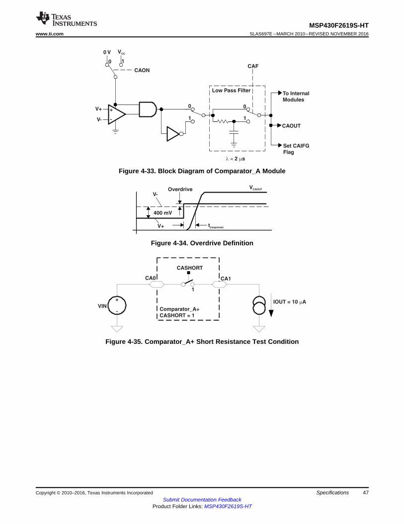
CA0
CASHORT
CA1
Comparator_A+
CASHORT = 1
VIN-
IOUT = 10 Am
1
+
OverdriveV-
400 mV
V+ t(response)
VCAOUT
0 V VCC
0 1
CAON
V+
V-
+
-
0
1
CAF
Low Pass FilterTo InternalModules
CAOUT
Set CAIFGFlag
0
1
l » m2 s
47
MSP430F2619S-HTwww.ti.com SLAS697E –MARCH 2010–REVISED NOVEMBER 2016
Submit Documentation FeedbackProduct Folder Links: MSP430F2619S-HT
SpecificationsCopyright © 2010–2016, Texas Instruments Incorporated
Figure 4-33. Block Diagram of Comparator_A Module
Figure 4-34. Overdrive Definition
Figure 4-35. Comparator_A+ Short Resistance Test Condition
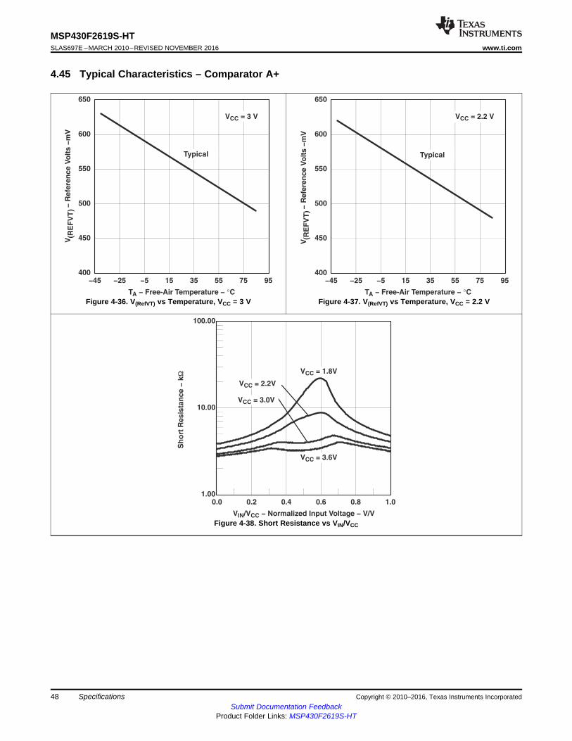
48
MSP430F2619S-HTSLAS697E –MARCH 2010–REVISED NOVEMBER 2016 www.ti.com
Submit Documentation FeedbackProduct Folder Links: MSP430F2619S-HT
Specifications Copyright © 2010–2016, Texas Instruments Incorporated
4.45 Typical Characteristics – Comparator A+
Figure 4-36. V(RefVT) vs Temperature, VCC = 3 V Figure 4-37. V(RefVT) vs Temperature, VCC = 2.2 V
Figure 4-38. Short Resistance vs VIN/VCC
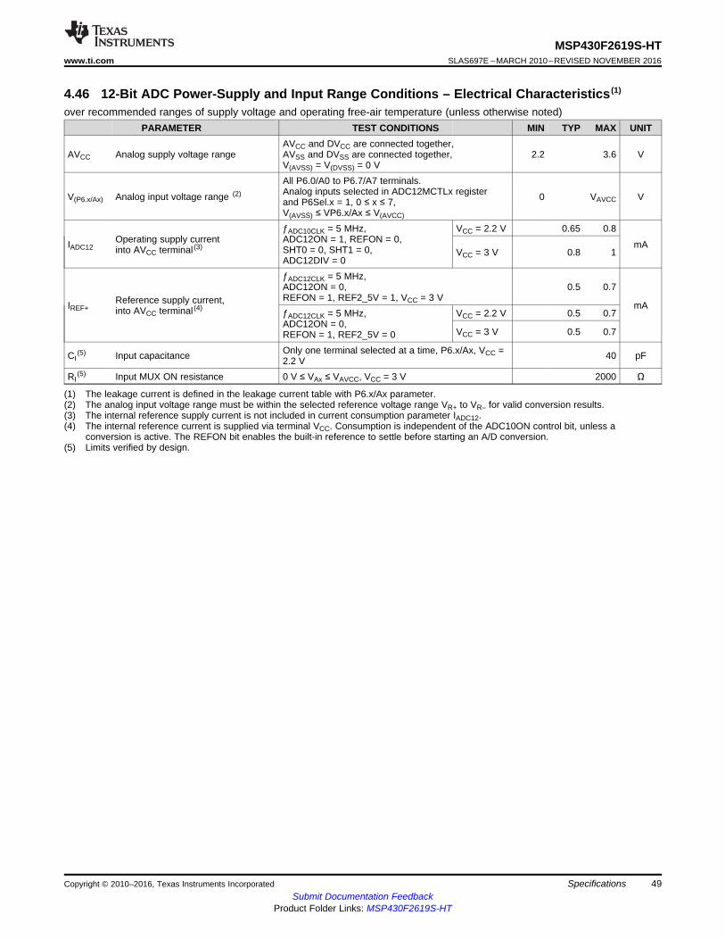
49
MSP430F2619S-HTwww.ti.com SLAS697E –MARCH 2010–REVISED NOVEMBER 2016
Submit Documentation FeedbackProduct Folder Links: MSP430F2619S-HT
SpecificationsCopyright © 2010–2016, Texas Instruments Incorporated
(1) The leakage current is defined in the leakage current table with P6.x/Ax parameter.(2) The analog input voltage range must be within the selected reference voltage range VR+ to VR– for valid conversion results.(3) The internal reference supply current is not included in current consumption parameter IADC12.(4) The internal reference current is supplied via terminal VCC. Consumption is independent of the ADC10ON control bit, unless a
conversion is active. The REFON bit enables the built-in reference to settle before starting an A/D conversion.(5) Limits verified by design.
4.46 12-Bit ADC Power-Supply and Input Range Conditions – Electrical Characteristics (1)
over recommended ranges of supply voltage and operating free-air temperature (unless otherwise noted)PARAMETER TEST CONDITIONS MIN TYP MAX UNIT
AVCC Analog supply voltage rangeAVCC and DVCC are connected together,AVSS and DVSS are connected together,V(AVSS) = V(DVSS) = 0 V
2.2 3.6 V
V(P6.x/Ax) Analog input voltage range (2)
All P6.0/A0 to P6.7/A7 terminals.Analog inputs selected in ADC12MCTLx registerand P6Sel.x = 1, 0 ≤ x ≤ 7,V(AVSS) ≤ VP6.x/Ax ≤ V(AVCC)
0 VAVCC V
IADC12Operating supply currentinto AVCC terminal (3)
ƒADC10CLK = 5 MHz,ADC12ON = 1, REFON = 0,SHT0 = 0, SHT1 = 0,ADC12DIV = 0
VCC = 2.2 V 0.65 0.8
mAVCC = 3 V 0.8 1
IREF+Reference supply current,into AVCC terminal (4)
ƒADC12CLK = 5 MHz,ADC12ON = 0,REFON = 1, REF2_5V = 1, VCC = 3 V
0.5 0.7
mAƒADC12CLK = 5 MHz,ADC12ON = 0,REFON = 1, REF2_5V = 0
VCC = 2.2 V 0.5 0.7
VCC = 3 V 0.5 0.7
CI(5) Input capacitance Only one terminal selected at a time, P6.x/Ax, VCC =
2.2 V 40 pF
RI(5) Input MUX ON resistance 0 V ≤ VAx ≤ VAVCC, VCC = 3 V 2000 Ω
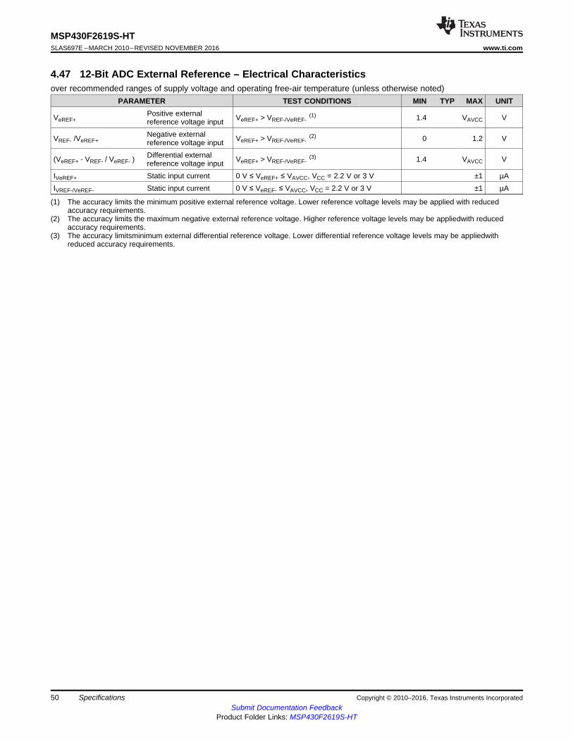
50
MSP430F2619S-HTSLAS697E –MARCH 2010–REVISED NOVEMBER 2016 www.ti.com
Submit Documentation FeedbackProduct Folder Links: MSP430F2619S-HT
Specifications Copyright © 2010–2016, Texas Instruments Incorporated
(1) The accuracy limits the minimum positive external reference voltage. Lower reference voltage levels may be applied with reducedaccuracy requirements.
(2) The accuracy limits the maximum negative external reference voltage. Higher reference voltage levels may be appliedwith reducedaccuracy requirements.
(3) The accuracy limitsminimum external differential reference voltage. Lower differential reference voltage levels may be appliedwithreduced accuracy requirements.
4.47 12-Bit ADC External Reference – Electrical Characteristicsover recommended ranges of supply voltage and operating free-air temperature (unless otherwise noted)
PARAMETER TEST CONDITIONS MIN TYP MAX UNIT
VeREF+Positive externalreference voltage input VeREF+ > VREF-/VeREF-
(1) 1.4 VAVCC V
VREF- /VeREF+Negative externalreference voltage input VeREF+ > VREF-/VeREF-
(2) 0 1.2 V
(VeREF+ - VREF- / VeREF- ) Differential externalreference voltage input VeREF+ > VREF-/VeREF-
(3) 1.4 VAVCC V
IVeREF+ Static input current 0 V ≤ VeREF+ ≤ VAVCC, VCC = 2.2 V or 3 V ±1 µAIVREF-/VeREF- Static input current 0 V ≤ VeREF- ≤ VAVCC, VCC = 2.2 V or 3 V ±1 µA
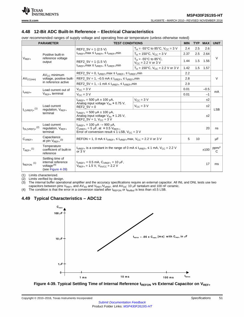
CVREF+
1mF
0
1 m s 10 m s 100 m stREFON
tREFON » .66 x CVREF+[m s] w ith CVREF+ in mF
100 mF
10 mF
51
MSP430F2619S-HTwww.ti.com SLAS697E –MARCH 2010–REVISED NOVEMBER 2016
Submit Documentation FeedbackProduct Folder Links: MSP430F2619S-HT
SpecificationsCopyright © 2010–2016, Texas Instruments Incorporated
(1) Limits characterized.(2) Limits verified by design.(3) The internal buffer operational amplifier and the accuracy specifications require an external capacitor. All INL and DNL tests use two
capacitors between pins VREF+ and AVSS and VREF-/VeREF- and AVSS: 10 μF tantalum and 100 nF ceramic.(4) The condition is that the error in a conversion started after tREFON or tRefBuf is less than ±0.5 LSB.
4.48 12-Bit ADC Built-In Reference – Electrical Characteristicsover recommended ranges of supply voltage and operating free-air temperature (unless otherwise noted)
PARAMETER TEST CONDITIONS MIN TYP MAX UNIT
VREF+
Positive built-inreference voltageoutput
REF2_5V = 1 (2.5 V)IVREF+max ≤ IVREF+ ≤ IVREF+min
TA = -55°C to 85°C, VCC = 3 V 2.4 2.5 2.6
VTA = 150°C, VCC = 3 V 2.37 2.5 2.64
REF2_5V = 1 (1.5 V)IVREF+max ≤ IVREF+ ≤ IVREF+min
TA = -55°C to 85°C,VCC = 2.2 V or 3 V 1.44 1.5 1.56
TA = 150°C, VCC = 2.2 V or 3 V 1.42 1.5 1.57
AVCC(min)
AVCC minimumvoltage, positive built-in reference active
REF2_5V = 0, IVREF+max ≤ IVREF+ ≤ IVREF+min 2.2VREF2_5V = 1, –0.5 mA ≤ IVREF+ ≤ IVREF+min 2.8
REF2_5V = 1, –1 mA ≤ IVREF+ ≤ IVREF+min 2.9
IVREF+Load current out ofVREF+ terminal
VCC = 3 V 0.01 –0.5mA
VCC = 3 V 0.01 –1
IL(VREF)+(1)
Load currentregulation, VREF+terminal
IVREF+ = 500 μA ± 100 μA,Analog input voltage VAx ≉ 0.75 V,REF2_5V = 0
VCC = 3 V ±2
LSBVCC = 3 V ±2
IVREF+ = 500 μA ± 100 μA,Analog input voltage VAx ≉ 1.25 V,REF2_5V = 1, VCC = 3 V
±2
IDL(VREF)+(2)
Load currentregulation, VREF+terminal
IVREF+ = 100 μA → 900 μA,CVREF+ = 5 μF, at ≉ 0.5 VREF+,Error of conversion result ≤ 1 LSB, VCC = 3 V
20 ns
CVREF+Capacitanceat pin VREF+
(3) REFON = 1, 0 mA ≤ IVREF+ ≤ IVREF+max, VCC = 2.2 V or 3 V 5 10 µF
TREF+(1)
Temperaturecoefficient of built-inreference
IVREF+ is a constant in the range of 0 mA ≤ IVREF+ ≤ 1 mA, VCC = 2.2 Vor 3 V ±100 ppm/°
C
tREFON(1)
Settling time ofinternal referencevoltage (4)
(see Figure 4-39)
IVREF+ = 0.5 mA, CVREF+ = 10 μF,VREF+ = 1.5 V, VAVCC = 2.2 V 17 ms
4.49 Typical Characteristics – ADC12
Figure 4-39. Typical Settling Time of Internal Reference tREFON vs External Capacitor on VREF+
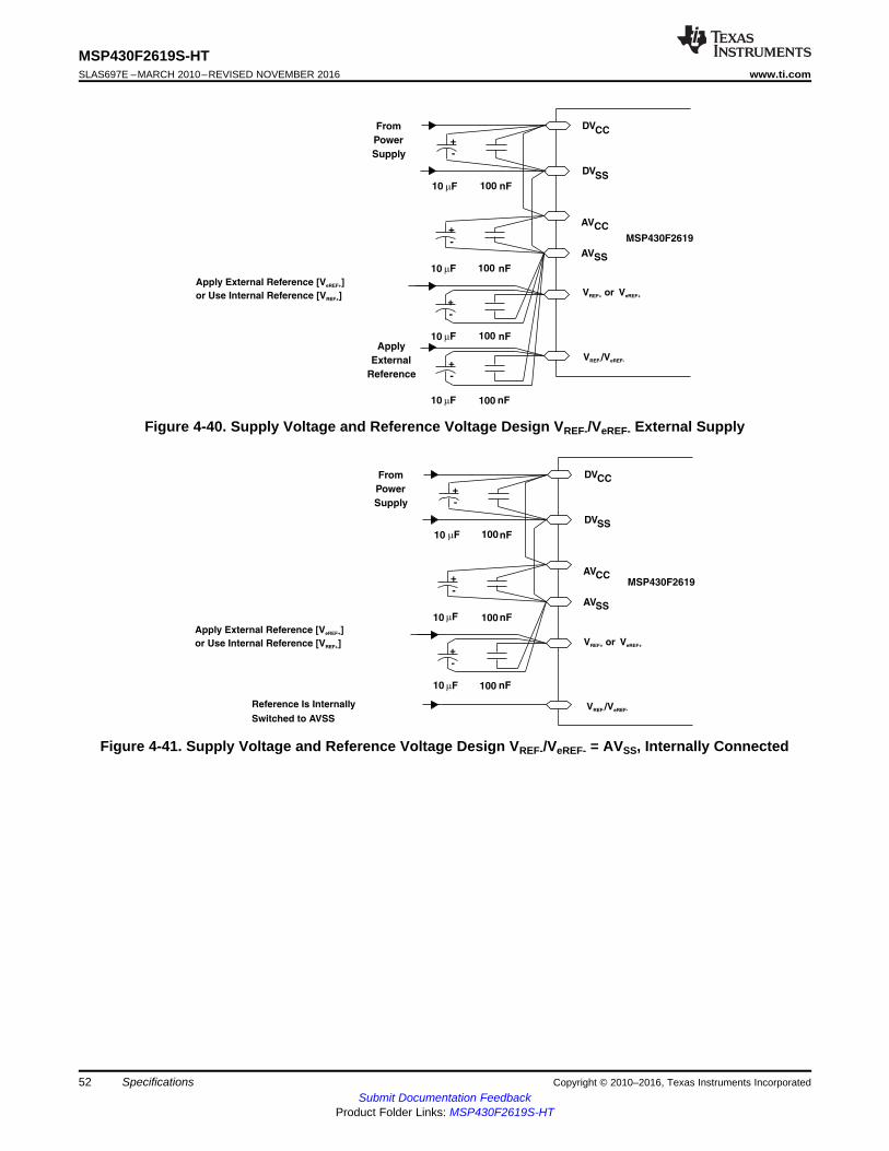
+
-
10 mF 100 nF
AVSS
MSP430F2619
+
-
10 mF 100 nF
AVCC
10 mF 100nF
DVSS
DVCCFrom
Power
Supply
+
-
Apply External Reference [V ]eREF+
or Use Internal Reference [V ]REF+V or VREF+ eREF+
V /VREF- eREF-Reference Is Internally
Switched to AVSS
+
-
10 mF 100 nF
AVSS
MSP430F2619
+
-
+
-
10 mF 100 nF
10 mF 100 nF
AVCC
10 mF 100 nF
DVSS
DVCCFrom
Power
Supply
Apply
External
Reference
+
-
Apply External Reference [V ]eREF+
or Use Internal Reference [V ]REF+V or VREF+ eREF+
V /VREF- eREF-
52
MSP430F2619S-HTSLAS697E –MARCH 2010–REVISED NOVEMBER 2016 www.ti.com
Submit Documentation FeedbackProduct Folder Links: MSP430F2619S-HT
Specifications Copyright © 2010–2016, Texas Instruments Incorporated
Figure 4-40. Supply Voltage and Reference Voltage Design VREF-/VeREF- External Supply
Figure 4-41. Supply Voltage and Reference Voltage Design VREF-/VeREF- = AVSS, Internally Connected
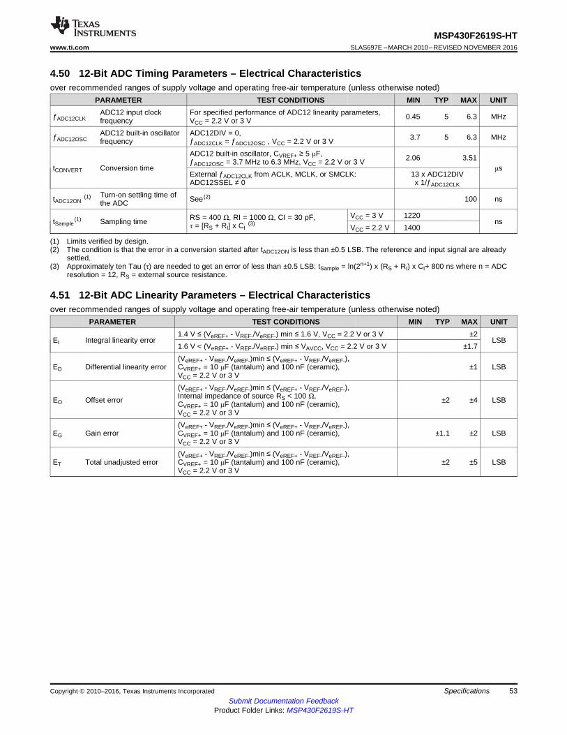
53
MSP430F2619S-HTwww.ti.com SLAS697E –MARCH 2010–REVISED NOVEMBER 2016
Submit Documentation FeedbackProduct Folder Links: MSP430F2619S-HT
SpecificationsCopyright © 2010–2016, Texas Instruments Incorporated
(1) Limits verified by design.(2) The condition is that the error in a conversion started after tADC12ON is less than ±0.5 LSB. The reference and input signal are already
settled.(3) Approximately ten Tau (τ) are needed to get an error of less than ±0.5 LSB: tSample = ln(2n+1) x (RS + RI) x CI+ 800 ns where n = ADC
resolution = 12, RS = external source resistance.
4.50 12-Bit ADC Timing Parameters – Electrical Characteristicsover recommended ranges of supply voltage and operating free-air temperature (unless otherwise noted)
PARAMETER TEST CONDITIONS MIN TYP MAX UNIT
ƒADC12CLKADC12 input clockfrequency
For specified performance of ADC12 linearity parameters,VCC = 2.2 V or 3 V 0.45 5 6.3 MHz
ƒADC12OSCADC12 built-in oscillatorfrequency
ADC12DIV = 0,ƒADC12CLK = ƒADC12OSC , VCC = 2.2 V or 3 V 3.7 5 6.3 MHz
tCONVERT Conversion time
ADC12 built-in oscillator, CVREF+ ≥ 5 μF,ƒADC12OSC = 3.7 MHz to 6.3 MHz, VCC = 2.2 V or 3 V 2.06 3.51
μsExternal ƒADC12CLK from ACLK, MCLK, or SMCLK:ADC12SSEL ≠ 0
13 x ADC12DIVx 1/ƒADC12CLK
tADC12ON(1) Turn-on settling time of
the ADC See (2) 100 ns
tSample(1) Sampling time RS = 400 Ω, RI = 1000 Ω, CI = 30 pF,
τ = [RS + RI] x CI(3)
VCC = 3 V 1220ns
VCC = 2.2 V 1400
4.51 12-Bit ADC Linearity Parameters – Electrical Characteristicsover recommended ranges of supply voltage and operating free-air temperature (unless otherwise noted)
PARAMETER TEST CONDITIONS MIN TYP MAX UNIT
EI Integral linearity error1.4 V ≤ (VeREF+ - VREF-/VeREF-) min ≤ 1.6 V, VCC = 2.2 V or 3 V ±2
LSB1.6 V < (VeREF+ - VREF-/VeREF-) min ≤ VAVCC, VCC = 2.2 V or 3 V ±1.7
ED Differential linearity error(VeREF+ - VREF-/VeREF-)min ≤ (VeREF+ - VREF-/VeREF-),CVREF+ = 10 μF (tantalum) and 100 nF (ceramic),VCC = 2.2 V or 3 V
±1 LSB
EO Offset error
(VeREF+ - VREF-/VeREF-)min ≤ (VeREF+ - VREF-/VeREF-),Internal impedance of source RS < 100 Ω,CVREF+ = 10 μF (tantalum) and 100 nF (ceramic),VCC = 2.2 V or 3 V
±2 ±4 LSB
EG Gain error(VeREF+ - VREF-/VeREF-)min ≤ (VeREF+ - VREF-/VeREF-),CVREF+ = 10 μF (tantalum) and 100 nF (ceramic),VCC = 2.2 V or 3 V
±1.1 ±2 LSB
ET Total unadjusted error(VeREF+ - VREF-/VeREF-)min ≤ (VeREF+ - VREF-/VeREF-),CVREF+ = 10 μF (tantalum) and 100 nF (ceramic),VCC = 2.2 V or 3 V
±2 ±5 LSB
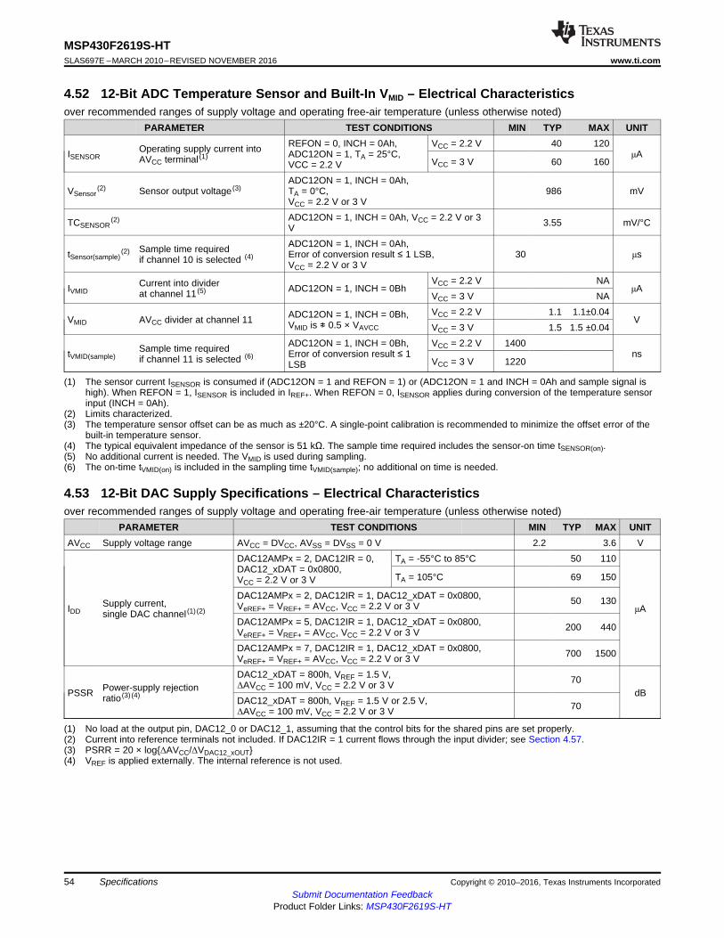
54
MSP430F2619S-HTSLAS697E –MARCH 2010–REVISED NOVEMBER 2016 www.ti.com
Submit Documentation FeedbackProduct Folder Links: MSP430F2619S-HT
Specifications Copyright © 2010–2016, Texas Instruments Incorporated
(1) The sensor current ISENSOR is consumed if (ADC12ON = 1 and REFON = 1) or (ADC12ON = 1 and INCH = 0Ah and sample signal ishigh). When REFON = 1, ISENSOR is included in IREF+. When REFON = 0, ISENSOR applies during conversion of the temperature sensorinput (INCH = 0Ah).
(2) Limits characterized.(3) The temperature sensor offset can be as much as ±20°C. A single-point calibration is recommended to minimize the offset error of the
built-in temperature sensor.(4) The typical equivalent impedance of the sensor is 51 kΩ. The sample time required includes the sensor-on time tSENSOR(on).(5) No additional current is needed. The VMID is used during sampling.(6) The on-time tVMID(on) is included in the sampling time tVMID(sample); no additional on time is needed.
4.52 12-Bit ADC Temperature Sensor and Built-In VMID – Electrical Characteristicsover recommended ranges of supply voltage and operating free-air temperature (unless otherwise noted)
PARAMETER TEST CONDITIONS MIN TYP MAX UNIT
ISENSOROperating supply current intoAVCC terminal (1)
REFON = 0, INCH = 0Ah,ADC12ON = 1, TA = 25°C,VCC = 2.2 V
VCC = 2.2 V 40 120μA
VCC = 3 V 60 160
VSensor(2) Sensor output voltage (3)
ADC12ON = 1, INCH = 0Ah,TA = 0°C,VCC = 2.2 V or 3 V
986 mV
TCSENSOR(2) ADC12ON = 1, INCH = 0Ah, VCC = 2.2 V or 3
V 3.55 mV/°C
tSensor(sample)(2) Sample time required
if channel 10 is selected (4)
ADC12ON = 1, INCH = 0Ah,Error of conversion result ≤ 1 LSB,VCC = 2.2 V or 3 V
30 μs
IVMIDCurrent into dividerat channel 11 (5) ADC12ON = 1, INCH = 0Bh
VCC = 2.2 V NAμA
VCC = 3 V NA
VMID AVCC divider at channel 11 ADC12ON = 1, INCH = 0Bh,VMID is ≉ 0.5 × VAVCC
VCC = 2.2 V 1.1 1.1±0.04V
VCC = 3 V 1.5 1.5 ±0.04
tVMID(sample)Sample time requiredif channel 11 is selected (6)
ADC12ON = 1, INCH = 0Bh,Error of conversion result ≤ 1LSB
VCC = 2.2 V 1400ns
VCC = 3 V 1220
(1) No load at the output pin, DAC12_0 or DAC12_1, assuming that the control bits for the shared pins are set properly.(2) Current into reference terminals not included. If DAC12IR = 1 current flows through the input divider; see Section 4.57.(3) PSRR = 20 × logΔAVCC/ΔVDAC12_xOUT(4) VREF is applied externally. The internal reference is not used.
4.53 12-Bit DAC Supply Specifications – Electrical Characteristicsover recommended ranges of supply voltage and operating free-air temperature (unless otherwise noted)
PARAMETER TEST CONDITIONS MIN TYP MAX UNITAVCC Supply voltage range AVCC = DVCC, AVSS = DVSS = 0 V 2.2 3.6 V
IDDSupply current,single DAC channel (1) (2)
DAC12AMPx = 2, DAC12IR = 0,DAC12_xDAT = 0x0800,VCC = 2.2 V or 3 V
TA = -55°C to 85°C 50 110
μA
TA = 105°C 69 150
DAC12AMPx = 2, DAC12IR = 1, DAC12_xDAT = 0x0800,VeREF+ = VREF+ = AVCC, VCC = 2.2 V or 3 V 50 130
DAC12AMPx = 5, DAC12IR = 1, DAC12_xDAT = 0x0800,VeREF+ = VREF+ = AVCC, VCC = 2.2 V or 3 V 200 440
DAC12AMPx = 7, DAC12IR = 1, DAC12_xDAT = 0x0800,VeREF+ = VREF+ = AVCC, VCC = 2.2 V or 3 V 700 1500
PSSR Power-supply rejectionratio (3) (4)
DAC12_xDAT = 800h, VREF = 1.5 V,ΔAVCC = 100 mV, VCC = 2.2 V or 3 V 70
dBDAC12_xDAT = 800h, VREF = 1.5 V or 2.5 V,ΔAVCC = 100 mV, VCC = 2.2 V or 3 V 70
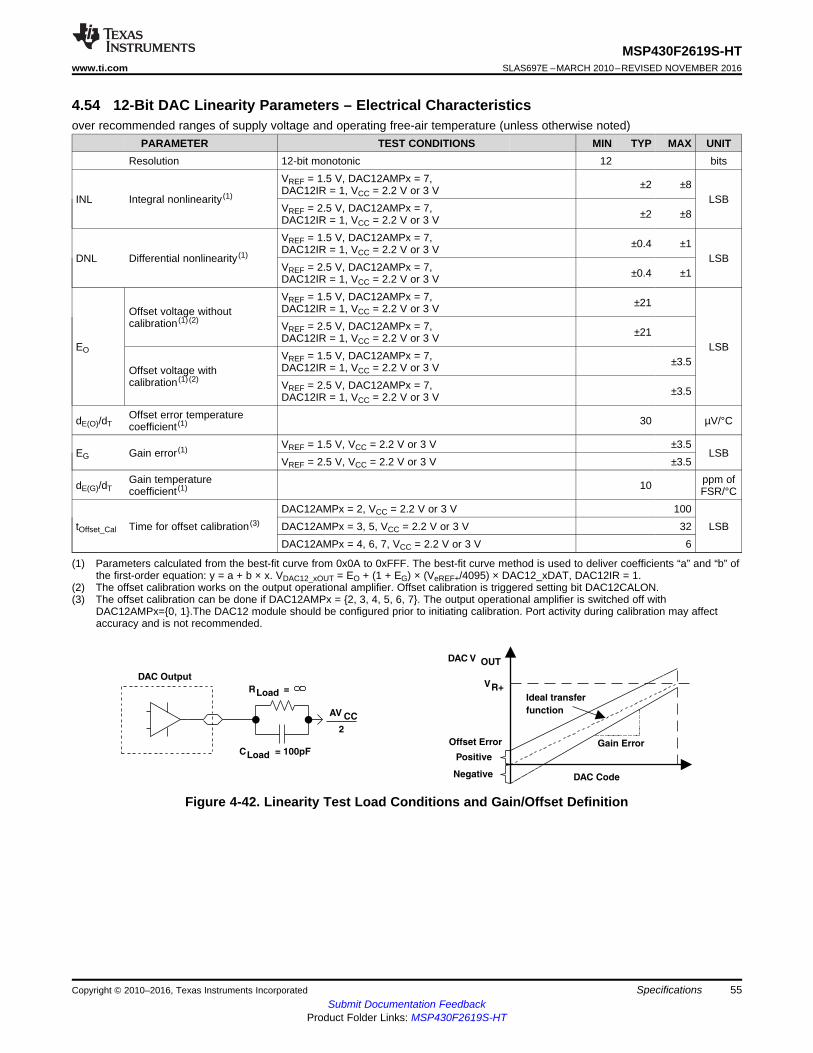
Positive
Negative
VR+
Gain ErrorOffset Error
DAC Code
DAC V OUT
Ideal transfer
function
RLoad =
AV CC
CLoad = 100pF
2
DAC Output
55
MSP430F2619S-HTwww.ti.com SLAS697E –MARCH 2010–REVISED NOVEMBER 2016
Submit Documentation FeedbackProduct Folder Links: MSP430F2619S-HT
SpecificationsCopyright © 2010–2016, Texas Instruments Incorporated
(1) Parameters calculated from the best-fit curve from 0x0A to 0xFFF. The best-fit curve method is used to deliver coefficients “a” and “b” ofthe first-order equation: y = a + b × x. VDAC12_xOUT = EO + (1 + EG) × (VeREF+/4095) × DAC12_xDAT, DAC12IR = 1.
(2) The offset calibration works on the output operational amplifier. Offset calibration is triggered setting bit DAC12CALON.(3) The offset calibration can be done if DAC12AMPx = 2, 3, 4, 5, 6, 7. The output operational amplifier is switched off with
DAC12AMPx=0, 1.The DAC12 module should be configured prior to initiating calibration. Port activity during calibration may affectaccuracy and is not recommended.
4.54 12-Bit DAC Linearity Parameters – Electrical Characteristicsover recommended ranges of supply voltage and operating free-air temperature (unless otherwise noted)
PARAMETER TEST CONDITIONS MIN TYP MAX UNITResolution 12-bit monotonic 12 bits
INL Integral nonlinearity (1)
VREF = 1.5 V, DAC12AMPx = 7,DAC12IR = 1, VCC = 2.2 V or 3 V ±2 ±8
LSBVREF = 2.5 V, DAC12AMPx = 7,DAC12IR = 1, VCC = 2.2 V or 3 V ±2 ±8
DNL Differential nonlinearity (1)
VREF = 1.5 V, DAC12AMPx = 7,DAC12IR = 1, VCC = 2.2 V or 3 V ±0.4 ±1
LSBVREF = 2.5 V, DAC12AMPx = 7,DAC12IR = 1, VCC = 2.2 V or 3 V ±0.4 ±1
EO
Offset voltage withoutcalibration (1) (2)
VREF = 1.5 V, DAC12AMPx = 7,DAC12IR = 1, VCC = 2.2 V or 3 V ±21
LSB
VREF = 2.5 V, DAC12AMPx = 7,DAC12IR = 1, VCC = 2.2 V or 3 V ±21
Offset voltage withcalibration (1) (2)
VREF = 1.5 V, DAC12AMPx = 7,DAC12IR = 1, VCC = 2.2 V or 3 V ±3.5
VREF = 2.5 V, DAC12AMPx = 7,DAC12IR = 1, VCC = 2.2 V or 3 V ±3.5
dE(O)/dTOffset error temperaturecoefficient (1) 30 µV/°C
EG Gain error (1) VREF = 1.5 V, VCC = 2.2 V or 3 V ±3.5LSB
VREF = 2.5 V, VCC = 2.2 V or 3 V ±3.5
dE(G)/dTGain temperaturecoefficient (1) 10 ppm of
FSR/°C
tOffset_Cal Time for offset calibration (3)
DAC12AMPx = 2, VCC = 2.2 V or 3 V 100LSBDAC12AMPx = 3, 5, VCC = 2.2 V or 3 V 32
DAC12AMPx = 4, 6, 7, VCC = 2.2 V or 3 V 6
Figure 4-42. Linearity Test Load Conditions and Gain/Offset Definition
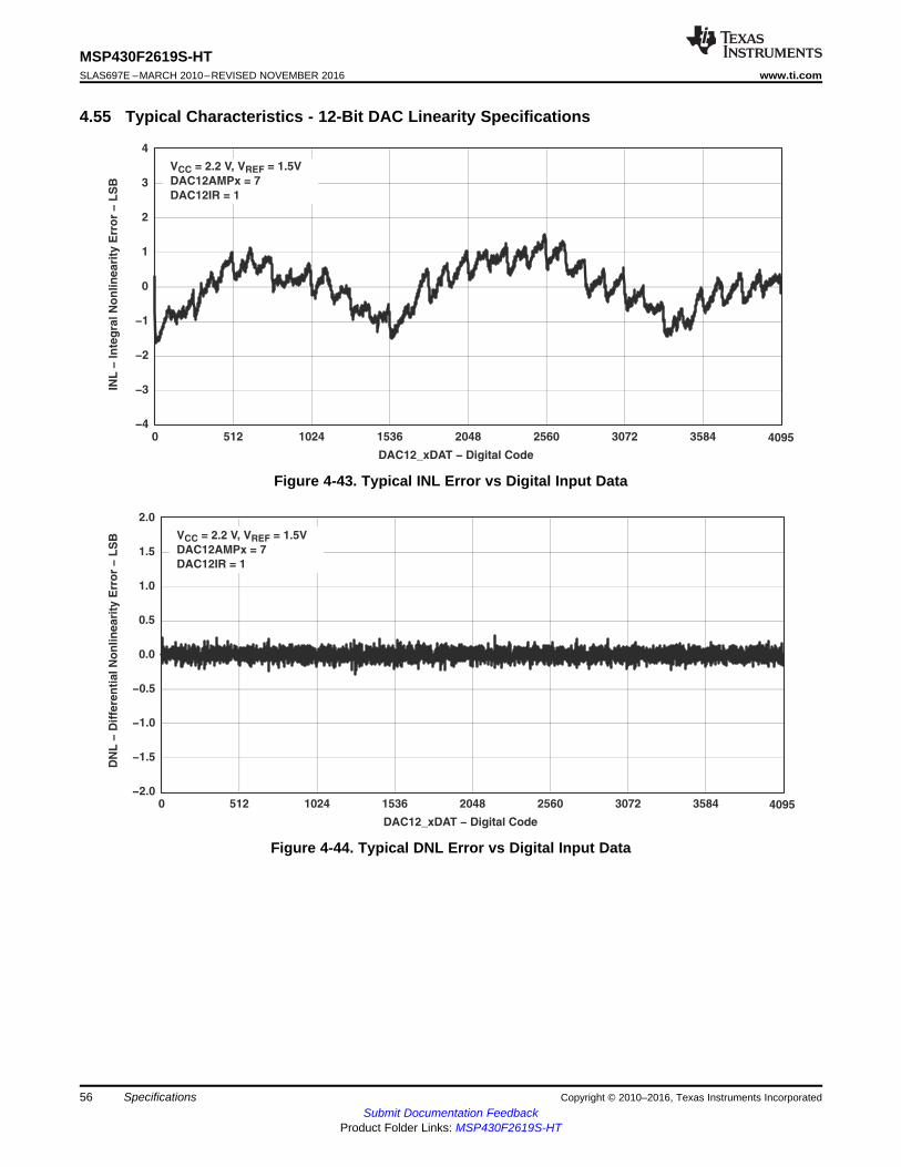
56
MSP430F2619S-HTSLAS697E –MARCH 2010–REVISED NOVEMBER 2016 www.ti.com
Submit Documentation FeedbackProduct Folder Links: MSP430F2619S-HT
Specifications Copyright © 2010–2016, Texas Instruments Incorporated
4.55 Typical Characteristics - 12-Bit DAC Linearity Specifications
Figure 4-43. Typical INL Error vs Digital Input Data
Figure 4-44. Typical DNL Error vs Digital Input Data
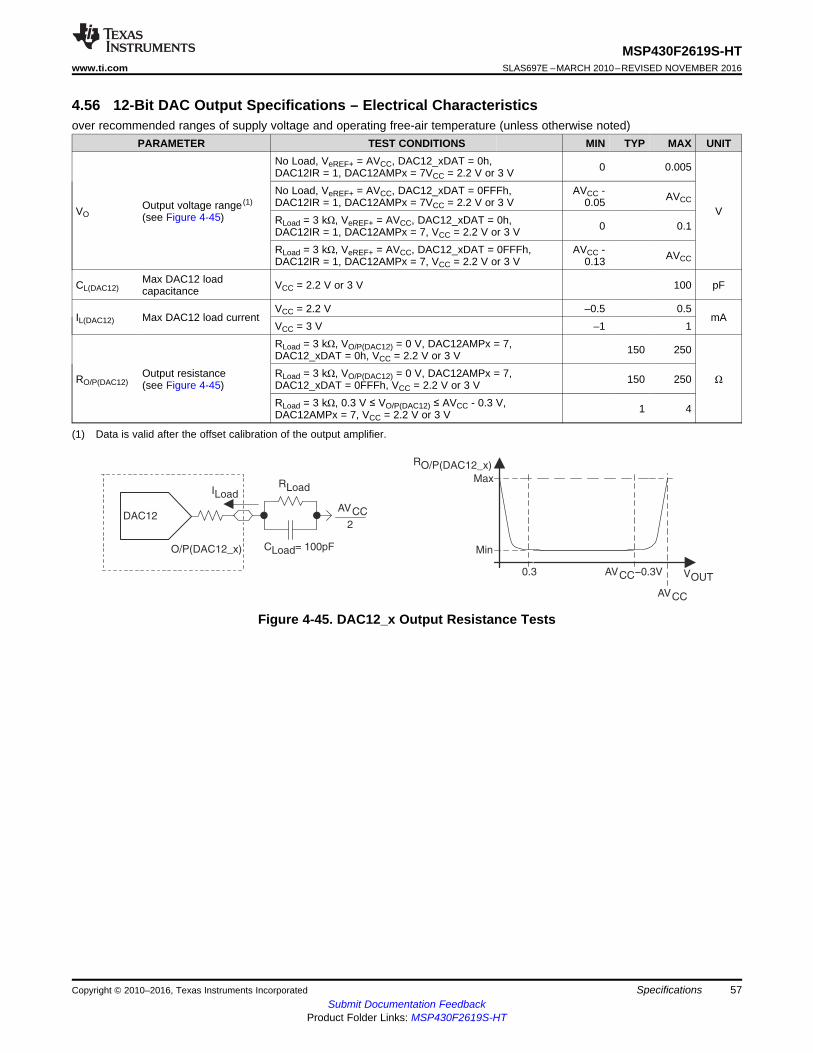
57
MSP430F2619S-HTwww.ti.com SLAS697E –MARCH 2010–REVISED NOVEMBER 2016
Submit Documentation FeedbackProduct Folder Links: MSP430F2619S-HT
SpecificationsCopyright © 2010–2016, Texas Instruments Incorporated
(1) Data is valid after the offset calibration of the output amplifier.
4.56 12-Bit DAC Output Specifications – Electrical Characteristicsover recommended ranges of supply voltage and operating free-air temperature (unless otherwise noted)
PARAMETER TEST CONDITIONS MIN TYP MAX UNIT
VOOutput voltage range (1)
(see Figure 4-45)
No Load, VeREF+ = AVCC, DAC12_xDAT = 0h,DAC12IR = 1, DAC12AMPx = 7VCC = 2.2 V or 3 V 0 0.005
V
No Load, VeREF+ = AVCC, DAC12_xDAT = 0FFFh,DAC12IR = 1, DAC12AMPx = 7VCC = 2.2 V or 3 V
AVCC -0.05 AVCC
RLoad = 3 kΩ, VeREF+ = AVCC, DAC12_xDAT = 0h,DAC12IR = 1, DAC12AMPx = 7, VCC = 2.2 V or 3 V 0 0.1
RLoad = 3 kΩ, VeREF+ = AVCC, DAC12_xDAT = 0FFFh,DAC12IR = 1, DAC12AMPx = 7, VCC = 2.2 V or 3 V
AVCC -0.13 AVCC
CL(DAC12)Max DAC12 loadcapacitance VCC = 2.2 V or 3 V 100 pF
IL(DAC12) Max DAC12 load currentVCC = 2.2 V –0.5 0.5
mAVCC = 3 V –1 1
RO/P(DAC12)Output resistance(see Figure 4-45)
RLoad = 3 kΩ, VO/P(DAC12) = 0 V, DAC12AMPx = 7,DAC12_xDAT = 0h, VCC = 2.2 V or 3 V 150 250
ΩRLoad = 3 kΩ, VO/P(DAC12) = 0 V, DAC12AMPx = 7,DAC12_xDAT = 0FFFh, VCC = 2.2 V or 3 V 150 250
RLoad = 3 kΩ, 0.3 V ≤ VO/P(DAC12) ≤ AVCC - 0.3 V,DAC12AMPx = 7, VCC = 2.2 V or 3 V 1 4
Figure 4-45. DAC12_x Output Resistance Tests
58
MSP430F2619S-HTSLAS697E –MARCH 2010–REVISED NOVEMBER 2016 www.ti.com
Submit Documentation FeedbackProduct Folder Links: MSP430F2619S-HT
Specifications Copyright © 2010–2016, Texas Instruments Incorporated
(1) For a full-scale output, the reference input voltage can be as high as 1/3 of the maximum output voltage swing (AVCC).(2) The maximum voltage applied at reference input voltage terminal VeREF+ = [AVCC - VE(O)] / [3 x (1 + EG)].(3) For a full-scale output, the reference input voltage can be as high as the maximum output voltage swing (AVCC).(4) The maximum voltage applied at reference input voltage terminal VeREF+ = [AVCC - VE(O)] / (1 + EG).(5) When DAC12IR = 1 and DAC12SREFx = 0 or 1 for both channels, the reference input resistive dividers for each DAC are in parallel
reducing the reference input resistance.
4.57 12-Bit DAC Reference Input Specifications – Electrical Characteristicsover recommended ranges of supply voltage and operating free-air temperature (unless otherwise noted)
PARAMETER TEST CONDITIONS MIN TYP MAX UNIT
VeREF+Reference input voltagerange
DAC12IR = 0 (1) (2), VCC = 2.2 V or 3 V AVCC/3 AVCC + 0.2V
DAC12IR = 1 (3) (4), VCC = 2.2 V or 3 V AVCC AVCC + 0.2
Ri(VREF+),Ri(VeREF+)
Reference inputresistance
DAC12_0 IR = DAC12_1 IR = 0,VCC = 2.2 V or 3 V 20 MΩ
DAC12_0 IR = 1, DAC12_1 IR = 0,VCC = 2.2 V or 3 V 40 48 56
kΩDAC12_0 IR = 0, DAC12_1 IR = 1,VCC = 2.2 V or 3 V
20 24 28DAC12_0 IR = 0, DAC12_1 IR = 1DAC12_0 SREFx = DAC12_1 SREFx (5),VCC = 2.2 V or 3 V
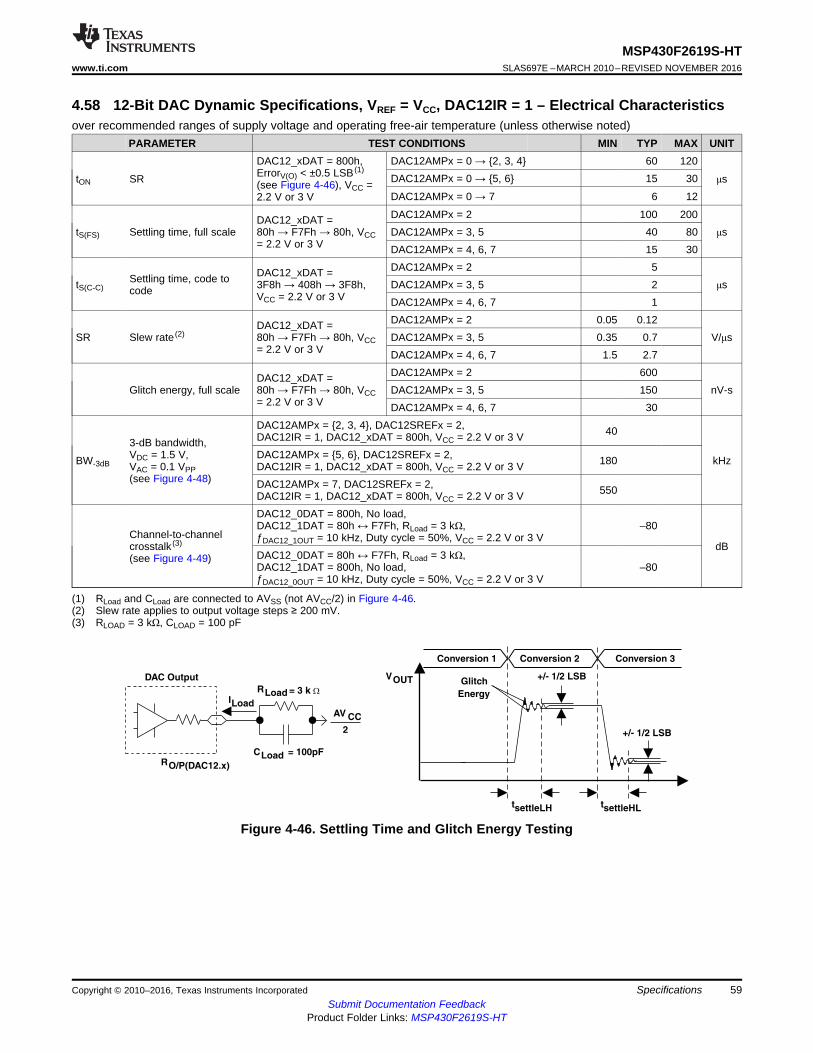
RLoad
AV CC
CLoad = 100pF
2
DAC Output
RO/P(DAC12.x)
ILoad
Conversion 1 Conversion 2
VOUT
Conversion 3
Glitch
Energy
+/- 1/2 LSB
+/- 1/2 LSB
tsettleLH tsettleHL
= 3 k W
59
MSP430F2619S-HTwww.ti.com SLAS697E –MARCH 2010–REVISED NOVEMBER 2016
Submit Documentation FeedbackProduct Folder Links: MSP430F2619S-HT
SpecificationsCopyright © 2010–2016, Texas Instruments Incorporated
(1) RLoad and CLoad are connected to AVSS (not AVCC/2) in Figure 4-46.(2) Slew rate applies to output voltage steps ≥ 200 mV.(3) RLOAD = 3 kΩ, CLOAD = 100 pF
4.58 12-Bit DAC Dynamic Specifications, VREF = VCC, DAC12IR = 1 – Electrical Characteristicsover recommended ranges of supply voltage and operating free-air temperature (unless otherwise noted)
PARAMETER TEST CONDITIONS MIN TYP MAX UNIT
tON SR
DAC12_xDAT = 800h,ErrorV(O) < ±0.5 LSB (1)
(see Figure 4-46), VCC =2.2 V or 3 V
DAC12AMPx = 0 → 2, 3, 4 60 120
μsDAC12AMPx = 0 → 5, 6 15 30
DAC12AMPx = 0 → 7 6 12
tS(FS) Settling time, full scaleDAC12_xDAT =80h → F7Fh → 80h, VCC= 2.2 V or 3 V
DAC12AMPx = 2 100 200μsDAC12AMPx = 3, 5 40 80
DAC12AMPx = 4, 6, 7 15 30
tS(C-C)Settling time, code tocode
DAC12_xDAT =3F8h → 408h → 3F8h,VCC = 2.2 V or 3 V
DAC12AMPx = 2 5μsDAC12AMPx = 3, 5 2
DAC12AMPx = 4, 6, 7 1
SR Slew rate (2)DAC12_xDAT =80h → F7Fh → 80h, VCC= 2.2 V or 3 V
DAC12AMPx = 2 0.05 0.12V/μsDAC12AMPx = 3, 5 0.35 0.7
DAC12AMPx = 4, 6, 7 1.5 2.7
Glitch energy, full scaleDAC12_xDAT =80h → F7Fh → 80h, VCC= 2.2 V or 3 V
DAC12AMPx = 2 600nV-sDAC12AMPx = 3, 5 150
DAC12AMPx = 4, 6, 7 30
BW-3dB
3-dB bandwidth,VDC = 1.5 V,VAC = 0.1 VPP(see Figure 4-48)
DAC12AMPx = 2, 3, 4, DAC12SREFx = 2,DAC12IR = 1, DAC12_xDAT = 800h, VCC = 2.2 V or 3 V 40
kHzDAC12AMPx = 5, 6, DAC12SREFx = 2,DAC12IR = 1, DAC12_xDAT = 800h, VCC = 2.2 V or 3 V 180
DAC12AMPx = 7, DAC12SREFx = 2,DAC12IR = 1, DAC12_xDAT = 800h, VCC = 2.2 V or 3 V 550
Channel-to-channelcrosstalk (3)
(see Figure 4-49)
DAC12_0DAT = 800h, No load,DAC12_1DAT = 80h ↔ F7Fh, RLoad = 3 kΩ,ƒDAC12_1OUT = 10 kHz, Duty cycle = 50%, VCC = 2.2 V or 3 V
–80
dBDAC12_0DAT = 80h ↔ F7Fh, RLoad = 3 kΩ,DAC12_1DAT = 800h, No load,ƒDAC12_0OUT = 10 kHz, Duty cycle = 50%, VCC = 2.2 V or 3 V
–80
Figure 4-46. Settling Time and Glitch Energy Testing
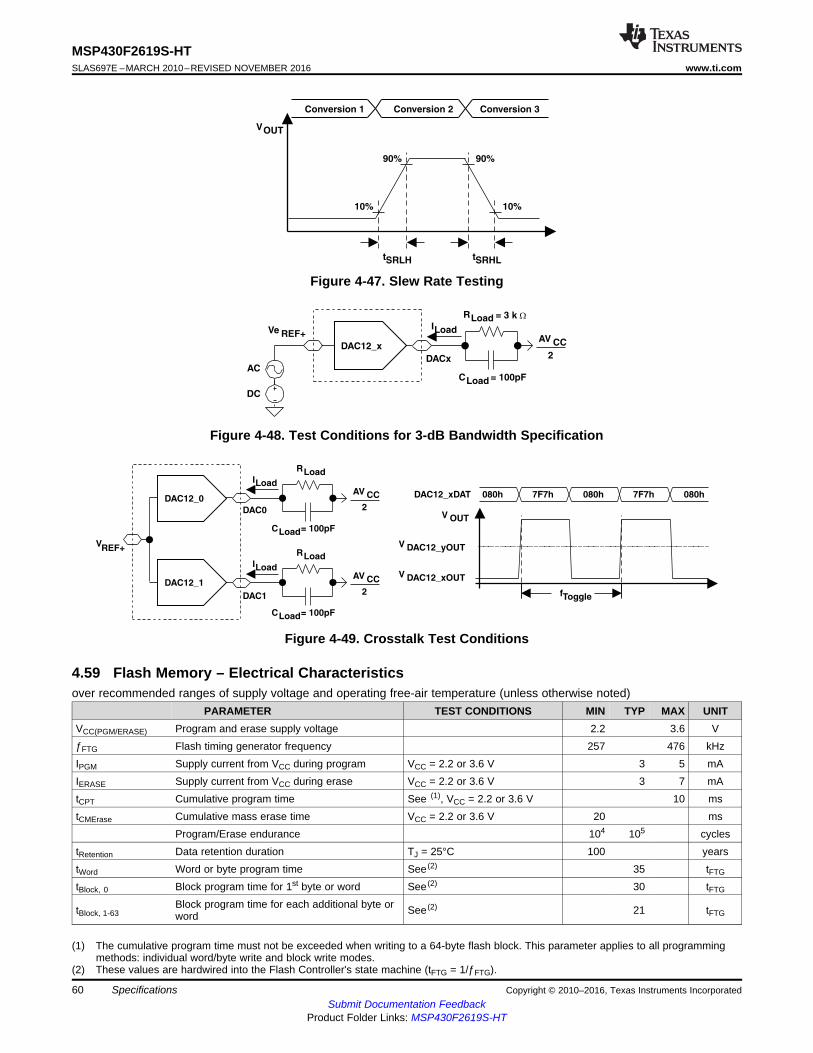
DAC12_xDAT 080h
V OUT
fToggle
7F7h
V DAC12_yOUT
080h 7F7h 080h
V DAC12_xOUT
REF+RLoad
AV CC
CLoad= 100pF
2
ILoad
DAC12_1
RLoad
AV CC
CLoad= 100pF
2
ILoad
DAC12_0
DAC0
DAC1
V
Ve REF+
AC
DC
RLoad
AV CC
CLoad = 100pF
2
ILoad
DAC12_x
DACx
= 3 k W
Conversion 1 Conversion 2
VOUT
Conversion 3
10%
tSRLH tSRHL
90%
10%
90%
60
MSP430F2619S-HTSLAS697E –MARCH 2010–REVISED NOVEMBER 2016 www.ti.com
Submit Documentation FeedbackProduct Folder Links: MSP430F2619S-HT
Specifications Copyright © 2010–2016, Texas Instruments Incorporated
Figure 4-47. Slew Rate Testing
Figure 4-48. Test Conditions for 3-dB Bandwidth Specification
Figure 4-49. Crosstalk Test Conditions
(1) The cumulative program time must not be exceeded when writing to a 64-byte flash block. This parameter applies to all programmingmethods: individual word/byte write and block write modes.
(2) These values are hardwired into the Flash Controller's state machine (tFTG = 1/ƒFTG).
4.59 Flash Memory – Electrical Characteristicsover recommended ranges of supply voltage and operating free-air temperature (unless otherwise noted)
PARAMETER TEST CONDITIONS MIN TYP MAX UNITVCC(PGM/ERASE) Program and erase supply voltage 2.2 3.6 VƒFTG Flash timing generator frequency 257 476 kHzIPGM Supply current from VCC during program VCC = 2.2 or 3.6 V 3 5 mAIERASE Supply current from VCC during erase VCC = 2.2 or 3.6 V 3 7 mAtCPT Cumulative program time See (1), VCC = 2.2 or 3.6 V 10 mstCMErase Cumulative mass erase time VCC = 2.2 or 3.6 V 20 ms
Program/Erase endurance 104 105 cyclestRetention Data retention duration TJ = 25°C 100 yearstWord Word or byte program time See (2) 35 tFTG
tBlock, 0 Block program time for 1st byte or word See (2) 30 tFTG
tBlock, 1-63Block program time for each additional byte orword See (2) 21 tFTG
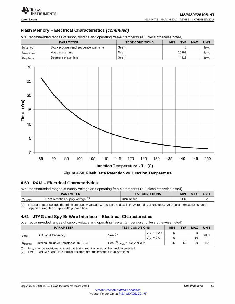
0
5
10
15
20
25
30
85 90 95 100 105 110 115 120 125 130 135 140 145 150
Junction Temperature - TJ (C)
Tim
e-
(Yrs
)
61
MSP430F2619S-HTwww.ti.com SLAS697E –MARCH 2010–REVISED NOVEMBER 2016
Submit Documentation FeedbackProduct Folder Links: MSP430F2619S-HT
SpecificationsCopyright © 2010–2016, Texas Instruments Incorporated
Flash Memory – Electrical Characteristics (continued)over recommended ranges of supply voltage and operating free-air temperature (unless otherwise noted)
PARAMETER TEST CONDITIONS MIN TYP MAX UNITtBlock, End Block program end-sequence wait time See (2) 6 tFTG
tMass Erase Mass erase time See (2) 10593 tFTG
tSeg Erase Segment erase time See (2) 4819 tFTG
Figure 4-50. Flash Data Retention vs Junction Temperature
(1) This parameter defines the minimum supply voltage VCC when the data in RAM remains unchanged. No program execution shouldhappen during this supply voltage condition.
4.60 RAM – Electrical Characteristicsover recommended ranges of supply voltage and operating free-air temperature (unless otherwise noted)
PARAMETER TEST CONDITIONS MIN MAX UNITV(RAMh) RAM retention supply voltage (1) CPU halted 1.6 V
(1) ƒTCK may be restricted to meet the timing requirements of the module selected.(2) TMS, TDI/TCLK, and TCK pullup resistors are implemented in all versions.
4.61 JTAG and Spy-Bi-Wire Interface – Electrical Characteristicsover recommended ranges of supply voltage and operating free-air temperature (unless otherwise noted)
PARAMETER TEST CONDITIONS MIN TYP MAX UNIT
ƒTCK TCK input frequency See (1) VCC = 2.2 V 0 5MHz
VCC = 3 V 0 10RInternal Internal pulldown resistance on TEST See (2), VCC = 2.2 V or 3 V 25 60 90 kΩ
62
MSP430F2619S-HTSLAS697E –MARCH 2010–REVISED NOVEMBER 2016 www.ti.com
Submit Documentation FeedbackProduct Folder Links: MSP430F2619S-HT
Specifications Copyright © 2010–2016, Texas Instruments Incorporated
(1) Once the fuse is blown, no further access to the MSP430 JTAG/Test and emulation features is possible. The JTAG block is switched tobypass mode.
4.62 JTAG Fuse (1) – Electrical Characteristicsover recommended ranges of supply voltage and operating free-air temperature (unless otherwise noted)
PARAMETER TEST CONDITIONS MIN MAX UNITVCC(FB) Supply voltage during fuse-blow condition TA = 25°C 2.5 VVFB Voltage level on TEST for fuse blow 6 7 VIFB Supply current into TEST during fuse blow 100 mAtFB Time to blow fuse 1 ms
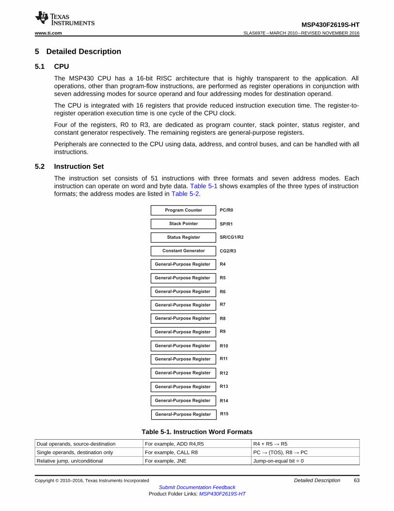
General-Purpose Register
Program Counter
Stack Pointer
Status Register
Constant Generator
General-Purpose Register
General-Purpose Register
General-Purpose Register
PC/R0
SP/R1
SR/CG1/R2
CG2/R3
R4
R5
R12
R13
General-Purpose Register
General-Purpose Register
R6
R7
General-Purpose Register
General-Purpose Register
R8
R9
General-Purpose Register
General-Purpose Register
R10
R11
General-Purpose Register
General-Purpose Register
R14
R15
63
MSP430F2619S-HTwww.ti.com SLAS697E –MARCH 2010–REVISED NOVEMBER 2016
Submit Documentation FeedbackProduct Folder Links: MSP430F2619S-HT
Detailed DescriptionCopyright © 2010–2016, Texas Instruments Incorporated
5 Detailed Description
5.1 CPUThe MSP430 CPU has a 16-bit RISC architecture that is highly transparent to the application. Alloperations, other than program-flow instructions, are performed as register operations in conjunction withseven addressing modes for source operand and four addressing modes for destination operand.
The CPU is integrated with 16 registers that provide reduced instruction execution time. The register-to-register operation execution time is one cycle of the CPU clock.
Four of the registers, R0 to R3, are dedicated as program counter, stack pointer, status register, andconstant generator respectively. The remaining registers are general-purpose registers.
Peripherals are connected to the CPU using data, address, and control buses, and can be handled with allinstructions.
5.2 Instruction SetThe instruction set consists of 51 instructions with three formats and seven address modes. Eachinstruction can operate on word and byte data. Table 5-1 shows examples of the three types of instructionformats; the address modes are listed in Table 5-2.
Table 5-1. Instruction Word Formats
Dual operands, source-destination For example, ADD R4,R5 R4 + R5 → R5Single operands, destination only For example, CALL R8 PC → (TOS), R8 → PCRelative jump, un/conditional For example, JNE Jump-on-equal bit = 0
64
MSP430F2619S-HTSLAS697E –MARCH 2010–REVISED NOVEMBER 2016 www.ti.com
Submit Documentation FeedbackProduct Folder Links: MSP430F2619S-HT
Detailed Description Copyright © 2010–2016, Texas Instruments Incorporated
(1) S = source(2) D = destination
Table 5-2. Address Mode Descriptions
ADDRESS MODE S (1) D (2) SYNTAX EXAMPLE OPERATIONRegister • • MOV Rs,Rd MOV R10,R11 R10 → R11Indexed • • MOV X(Rn),Y(Rm) MOV 2(R5),6(R6) M(2+R5) → M(6+R6)
Symbolic (PC relative) • • MOV EDE,TONI M(EDE) → M(TONI)Absolute • • MOV &MEM,&TCDAT M(MEM) → M(TCDAT)Indirect • MOV @Rn,Y(Rm) MOV @R10,Tab(R6) M(R10) → M(Tab+R6)
Indirect autoincrement • MOV @Rn+,Rm MOV @R10+,R11 M(R10) → R11R10 + 2 → R10
Immediate • MOV #X,TONI MOV #45,TONI #45 → M(TONI)
5.3 Operating ModesThe MSP430 has one active mode and five software selectable low-power modes of operation. Aninterrupt event can wake up the device from any of the five low-power modes, service the request andrestore back to the low-power mode on return from the interrupt program.
The following six operating modes can be configured by software:• Active mode ( AM)
– All clocks are active.• Low-power mode 0 (LPM0)
– CPU is disabled.– ACLK and SMCLK remain active. MCLK is disabled.
• Low-power mode 1 (LPM1)– CPU is disabled.– ACLK and SMCLK remain active. MCLK is disabled.– DCO’s DC generator is disabled if DCO not used in active mode.
• Low-power mode 2 (LPM2)– CPU is disabled.– MCLK and SMCLK are disabled.– DCO's dc-generator remains enabled.– ACLK remains active
• Low-power mode 3 (LPM3)– CPU is disabled.– MCLK and SMCLK are disabled.– DCO's dc-generator is disabled.– ACLK remains active.
• Low-power mode 4 (LPM4)– CPU is disabled.– ACLK is disabled.– MCLK and SMCLK are disabled.– DCO's dc-generator is disabled.– Crystal oscillator is stopped.
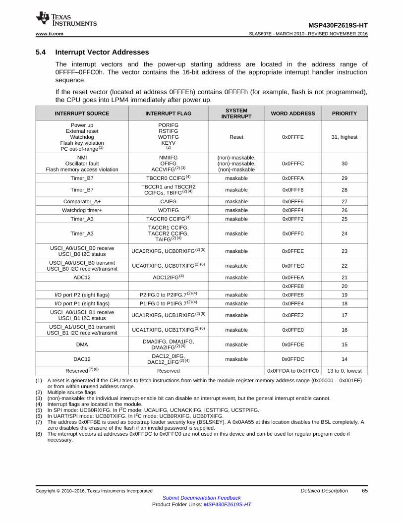
65
MSP430F2619S-HTwww.ti.com SLAS697E –MARCH 2010–REVISED NOVEMBER 2016
Submit Documentation FeedbackProduct Folder Links: MSP430F2619S-HT
Detailed DescriptionCopyright © 2010–2016, Texas Instruments Incorporated
(1) A reset is generated if the CPU tries to fetch instructions from within the module register memory address range (0x00000 – 0x001FF)or from within unused address range.
(2) Multiple source flags(3) (non)-maskable: the individual interrupt-enable bit can disable an interrupt event, but the general interrupt enable cannot.(4) Interrupt flags are located in the module.(5) In SPI mode: UCB0RXIFG. In I2C mode: UCALIFG, UCNACKIFG, ICSTTIFG, UCSTPIFG.(6) In UART/SPI mode: UCB0TXIFG. In I2C mode: UCB0RXIFG, UCB0TXIFG.(7) The address 0x0FFBE is used as bootstrap loader security key (BSLSKEY). A 0x0AA55 at this location disables the BSL completely. A
zero disables the erasure of the flash if an invalid password is supplied.(8) The interrupt vectors at addresses 0x0FFDC to 0x0FFC0 are not used in this device and can be used for regular program code if
necessary.
5.4 Interrupt Vector AddressesThe interrupt vectors and the power-up starting address are located in the address range of0FFFF–0FFC0h. The vector contains the 16-bit address of the appropriate interrupt handler instructionsequence.
If the reset vector (located at address 0FFFEh) contains 0FFFFh (for example, flash is not programmed),the CPU goes into LPM4 immediately after power up.
INTERRUPT SOURCE INTERRUPT FLAG SYSTEMINTERRUPT WORD ADDRESS PRIORITY
Power upExternal reset
WatchdogFlash key violationPC out-of-range (1)
PORIFGRSTIFGWDTIFG
KEYV(2)
Reset 0x0FFFE 31, highest
NMIOscillator fault
Flash memory access violation
NMIIFGOFIFG
ACCVIFG (2) (3)
(non)-maskable,(non)-maskable,(non)-maskable
0x0FFFC 30
Timer_B7 TBCCR0 CCIFG (4) maskable 0x0FFFA 29
Timer_B7 TBCCR1 and TBCCR2CCIFGs, TBIFG (2) (4) maskable 0x0FFF8 28
Comparator_A+ CAIFG maskable 0x0FFF6 27Watchdog timer+ WDTIFG maskable 0x0FFF4 26
Timer_A3 TACCR0 CCIFG (4) maskable 0x0FFF2 25
Timer_A3TACCR1 CCIFG,TACCR2 CCIFG,
TAIFG (2) (4)maskable 0x0FFF0 24
USCI_A0/USCI_B0 receiveUSCI_B0 I2C status UCA0RXIFG, UCB0RXIFG (2) (5) maskable 0x0FFEE 23
USCI_A0/USCI_B0 transmitUSCI_B0 I2C receive/transmit UCA0TXIFG, UCB0TXIFG (2) (6) maskable 0x0FFEC 22
ADC12 ADC12IFG (4) maskable 0x0FFEA 210x0FFE8 20
I/O port P2 (eight flags) P2IFG.0 to P2IFG.7 (2) (4) maskable 0x0FFE6 19I/O port P1 (eight flags) P1IFG.0 to P1IFG.7 (2) (4) maskable 0x0FFE4 18
USCI_A0/USCI_B1 receiveUSCI_B1 I2C status UCA1RXIFG, UCB1RXIFG (2) (5) maskable 0x0FFE2 17
USCI_A1/USCI_B1 transmitUSCI_B1 I2C receive/transmit UCA1TXIFG, UCB1TXIFG (2) (6) maskable 0x0FFE0 16
DMA DMA0IFG, DMA1IFG,DMA2IFG (2) (4) maskable 0x0FFDE 15
DAC12 DAC12_0IFG,DAC12_1IFG (2) (4) maskable 0x0FFDC 14
Reserved (7) (8) Reserved 0x0FFDA to 0x0FFC0 13 to 0, lowest
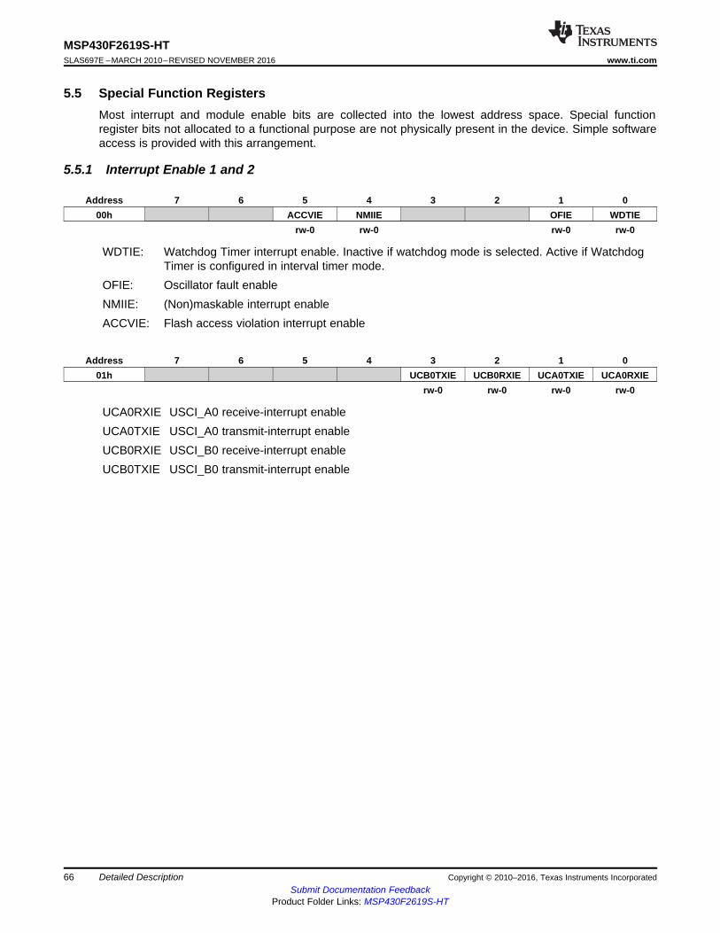
66
MSP430F2619S-HTSLAS697E –MARCH 2010–REVISED NOVEMBER 2016 www.ti.com
Submit Documentation FeedbackProduct Folder Links: MSP430F2619S-HT
Detailed Description Copyright © 2010–2016, Texas Instruments Incorporated
5.5 Special Function RegistersMost interrupt and module enable bits are collected into the lowest address space. Special functionregister bits not allocated to a functional purpose are not physically present in the device. Simple softwareaccess is provided with this arrangement.
5.5.1 Interrupt Enable 1 and 2
Address 7 6 5 4 3 2 1 000h ACCVIE NMIIE OFIE WDTIE
rw-0 rw-0 rw-0 rw-0
WDTIE: Watchdog Timer interrupt enable. Inactive if watchdog mode is selected. Active if WatchdogTimer is configured in interval timer mode.
OFIE: Oscillator fault enableNMIIE: (Non)maskable interrupt enableACCVIE: Flash access violation interrupt enable
Address 7 6 5 4 3 2 1 001h UCB0TXIE UCB0RXIE UCA0TXIE UCA0RXIE
rw-0 rw-0 rw-0 rw-0
UCA0RXIE USCI_A0 receive-interrupt enableUCA0TXIE USCI_A0 transmit-interrupt enableUCB0RXIE USCI_B0 receive-interrupt enableUCB0TXIE USCI_B0 transmit-interrupt enable
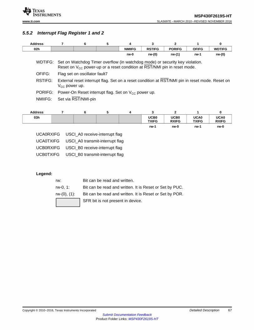
67
MSP430F2619S-HTwww.ti.com SLAS697E –MARCH 2010–REVISED NOVEMBER 2016
Submit Documentation FeedbackProduct Folder Links: MSP430F2619S-HT
Detailed DescriptionCopyright © 2010–2016, Texas Instruments Incorporated
5.5.2 Interrupt Flag Register 1 and 2
Address 7 6 5 4 3 2 1 002h NMIIFG RSTIFG PORIFG OFIFG WDTIFG
rw-0 rw-(0) rw-(1) rw-1 rw-(0)
WDTIFG: Set on Watchdog Timer overflow (in watchdog mode) or security key violation.Reset on VCC power-up or a reset condition at RST/NMI pin in reset mode.
OFIFG: Flag set on oscillator fault7RSTIFG: External reset interrupt flag. Set on a reset condition at RST/NMI pin in reset mode. Reset on
VCC power up.PORIFG: Power-On Reset interrupt flag. Set on VCC power up.NMIIFG: Set via RST/NMI-pin
Address 7 6 5 4 3 2 1 003h UCB0
TXIFGUCB0RXIFG
UCA0TXIFG
UCA0RXIFG
rw-1 rw-0 rw-1 rw-0
UCA0RXIFG USCI_A0 receive-interrupt flagUCA0TXIFG USCI_A0 transmit-interrupt flagUCB0RXIFG USCI_B0 receive-interrupt flagUCB0TXIFG USCI_B0 transmit-interrupt flag
xxx
Legend:rw: Bit can be read and written.rw-0, 1: Bit can be read and written. It is Reset or Set by PUC.rw-(0), (1): Bit can be read and written. It is Reset or Set by POR.
SFR bit is not present in device.
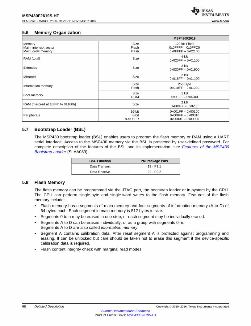
68
MSP430F2619S-HTSLAS697E –MARCH 2010–REVISED NOVEMBER 2016 www.ti.com
Submit Documentation FeedbackProduct Folder Links: MSP430F2619S-HT
Detailed Description Copyright © 2010–2016, Texas Instruments Incorporated
5.6 Memory OrganizationMSP430F2619
MemoryMain: interrupt vectorMain: code memory
SizeFlashFlash
120 kB Flash0x0FFFF – 0x0FFC00x0FFFF – 0x02100
RAM (total) Size 4 kB0x020FF -- 0x01100
Extended Size 2 kB0x020FF -- 0x01900
Mirrored Size 2 kB0x018FF -- 0x01100
Information memory SizeFlash
256 Byte0x010FF – 0x01000
Boot memory SizeROM
1 kB0x0FFF – 0x0C00
RAM (mirrored at 18FFh to 01100h) Size 2 kB0x009FF – 0x0200
Peripherals16-bit
8-bit8-bit SFR
0x001FF – 0x001000x000FF – 0x000100x0000F – 0x00000
5.7 Bootstrap Loader (BSL)The MSP430 bootstrap loader (BSL) enables users to program the flash memory or RAM using a UARTserial interface. Access to the MSP430 memory via the BSL is protected by user-defined password. Forcomplete description of the features of the BSL and its implementation, see Features of the MSP430Bootstrap Loader (SLAA089).
BSL Function PM Package PinsData Transmit 13 - P1.1Data Receive 22 - P2.2
5.8 Flash MemoryThe flash memory can be programmed via the JTAG port, the bootstrap loader or in-system by the CPU.The CPU can perform single-byte and single-word writes to the flash memory. Features of the flashmemory include:• Flash memory has n segments of main memory and four segments of information memory (A to D) of
64 bytes each. Each segment in main memory is 512 bytes in size.• Segments 0 to n may be erased in one step, or each segment may be individually erased.• Segments A to D can be erased individually, or as a group with segments 0–n.
Segments A to D are also called information memory.• Segment A contains calibration data. After reset segment A is protected against programming and
erasing. It can be unlocked but care should be taken not to erase this segment if the device-specificcalibration data is required.
• Flash content integrity check with marginal read modes.
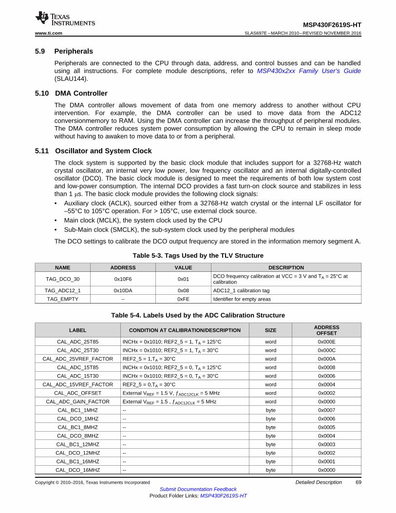
69
MSP430F2619S-HTwww.ti.com SLAS697E –MARCH 2010–REVISED NOVEMBER 2016
Submit Documentation FeedbackProduct Folder Links: MSP430F2619S-HT
Detailed DescriptionCopyright © 2010–2016, Texas Instruments Incorporated
5.9 PeripheralsPeripherals are connected to the CPU through data, address, and control busses and can be handledusing all instructions. For complete module descriptions, refer to MSP430x2xx Family User's Guide(SLAU144).
5.10 DMA ControllerThe DMA controller allows movement of data from one memory address to another without CPUintervention. For example, the DMA controller can be used to move data from the ADC12conversionmemory to RAM. Using the DMA controller can increase the throughput of peripheral modules.The DMA controller reduces system power consumption by allowing the CPU to remain in sleep modewithout having to awaken to move data to or from a peripheral.
5.11 Oscillator and System ClockThe clock system is supported by the basic clock module that includes support for a 32768-Hz watchcrystal oscillator, an internal very low power, low frequency oscillator and an internal digitally-controlledoscillator (DCO). The basic clock module is designed to meet the requirements of both low system costand low-power consumption. The internal DCO provides a fast turn-on clock source and stabilizes in lessthan 1 μs. The basic clock module provides the following clock signals:• Auxiliary clock (ACLK), sourced either from a 32768-Hz watch crystal or the internal LF oscillator for
–55°C to 105°C operation. For > 105°C, use external clock source.• Main clock (MCLK), the system clock used by the CPU• Sub-Main clock (SMCLK), the sub-system clock used by the peripheral modules
The DCO settings to calibrate the DCO output frequency are stored in the information memory segment A.
Table 5-3. Tags Used by the TLV Structure
NAME ADDRESS VALUE DESCRIPTION
TAG_DCO_30 0x10F6 0x01 DCO frequency calibration at VCC = 3 V and TA = 25°C atcalibration
TAG_ADC12_1 0x10DA 0x08 ADC12_1 calibration tagTAG_EMPTY -- 0xFE Identifier for empty areas
Table 5-4. Labels Used by the ADC Calibration Structure
LABEL CONDITION AT CALIBRATION/DESCRIPTION SIZE ADDRESSOFFSET
CAL_ADC_25T85 INCHx = 0x1010; REF2_5 = 1, TA = 125°C word 0x000ECAL_ADC_25T30 INCHx = 0x1010; REF2_5 = 1, TA = 30°C word 0x000C
CAL_ADC_25VREF_FACTOR REF2_5 = 1,TA = 30°C word 0x000ACAL_ADC_15T85 INCHx = 0x1010; REF2_5 = 0, TA = 125°C word 0x0008CAL_ADC_15T30 INCHx = 0x1010; REF2_5 = 0, TA = 30°C word 0x0006
CAL_ADC_15VREF_FACTOR REF2_5 = 0,TA = 30°C word 0x0004CAL_ADC_OFFSET External VREF = 1.5 V, ƒADC12CLK = 5 MHz word 0x0002
CAL_ADC_GAIN_FACTOR External VREF = 1.5 , ƒADC12CLK = 5 MHz word 0x0000CAL_BC1_1MHZ -- byte 0x0007CAL_DCO_1MHZ -- byte 0x0006CAL_BC1_8MHZ -- byte 0x0005CAL_DCO_8MHZ -- byte 0x0004CAL_BC1_12MHZ -- byte 0x0003CAL_DCO_12MHZ -- byte 0x0002CAL_BC1_16MHZ -- byte 0x0001CAL_DCO_16MHZ -- byte 0x0000
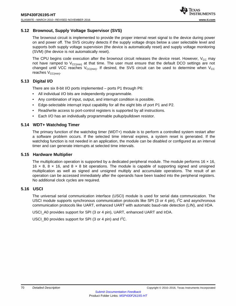
70
MSP430F2619S-HTSLAS697E –MARCH 2010–REVISED NOVEMBER 2016 www.ti.com
Submit Documentation FeedbackProduct Folder Links: MSP430F2619S-HT
Detailed Description Copyright © 2010–2016, Texas Instruments Incorporated
5.12 Brownout, Supply Voltage Supervisor (SVS)The brownout circuit is implemented to provide the proper internal reset signal to the device during poweron and power off. The SVS circuitry detects if the supply voltage drops below a user selectable level andsupports both supply voltage supervision (the device is automatically reset) and supply voltage monitoring(SVM) (the device is not automatically reset).
The CPU begins code execution after the brownout circuit releases the device reset. However, VCC maynot have ramped to VCC(min) at that time. The user must ensure that the default DCO settings are notchanged until VCC reaches VCC(min). If desired, the SVS circuit can be used to determine when VCCreaches VCC(min).
5.13 Digital I/OThere are six 8-bit I/O ports implemented – ports P1 through P6:• All individual I/O bits are independently programmable.• Any combination of input, output, and interrupt condition is possible.• Edge-selectable interrupt input capability for all the eight bits of port P1 and P2.• Read/write access to port-control registers is supported by all instructions.• Each I/O has an individually programmable pullup/pulldown resistor.
5.14 WDT+ Watchdog TimerThe primary function of the watchdog timer (WDT+) module is to perform a controlled system restart aftera software problem occurs. If the selected time interval expires, a system reset is generated. If thewatchdog function is not needed in an application, the module can be disabled or configured as an intervaltimer and can generate interrupts at selected time intervals.
5.15 Hardware MultiplierThe multiplication operation is supported by a dedicated peripheral module. The module performs 16 × 16,16 × 8, 8 × 16, and 8 × 8 bit operations. The module is capable of supporting signed and unsignedmultiplication as well as signed and unsigned multiply and accumulate operations. The result of anoperation can be accessed immediately after the operands have been loaded into the peripheral registers.No additional clock cycles are required.
5.16 USCIThe universal serial communication interface (USCI) module is used for serial data communication. TheUSCI module supports synchronous communication protocols like SPI (3 or 4 pin), I2C and asynchronouscommunication protocols like UART, enhanced UART with automatic baud-rate detection (LIN), and IrDA.
USCI_A0 provides support for SPI (3 or 4 pin), UART, enhanced UART and IrDA.
USCI_B0 provides support for SPI (3 or 4 pin) and I2C.
71
MSP430F2619S-HTwww.ti.com SLAS697E –MARCH 2010–REVISED NOVEMBER 2016
Submit Documentation FeedbackProduct Folder Links: MSP430F2619S-HT
Detailed DescriptionCopyright © 2010–2016, Texas Instruments Incorporated
5.17 Timer_A3Timer_A3 is a 16-bit timer/counter with three capture/compare registers. Timer_A3 can support multiplecapture/compares, PWM outputs, and interval timing. Timer_A3 also has extensive interrupt capabilities.Interrupts may be generated from the counter on overflow conditions and from each of thecapture/compare registers.
Table 5-5. TIMER_A3 Signal Connections
INPUT PINNO.
DEVICEINPUT
SIGNAL
MODULEINPUTNAME
MODULEBLOCK
MODULE USIGNAL
OUTPUTPIN NO.
12 - P1.0 TACLK TACLK
Timer NAACLK ACLK
SMCLK SMCLK21 - P2.1 TAINCLK INCLK13 - P1.1 TA0 CCI0A
CCR0 TA0
13 - P1.122 - P2.2 TA0 CCI0B 17 - P1.5
DVSS GND 27 - P2.7DVCC VCC
14 - P1.2 TA1 CCI1A
CCR1 TA1
14 - P1.2CAOUT(internal) CCI1B 18 - P1.6
DVSS GND 23 - P2.3
DVCC VCCADC12
(internal)DAC12_0(internal)DAC12_1(internal)
15 - P1.3 TA2 CCI2A
CCR2 TA2
15 - P1.3ACLK
(internal) CCI2B 19 - P1.7
DVSS GND 24 - P2.4DVCC VCC
72
MSP430F2619S-HTSLAS697E –MARCH 2010–REVISED NOVEMBER 2016 www.ti.com
Submit Documentation FeedbackProduct Folder Links: MSP430F2619S-HT
Detailed Description Copyright © 2010–2016, Texas Instruments Incorporated
5.18 Timer_B7Timer_B7 is a 16-bit timer/counter with three capture/compare registers. Timer_B7 can support multiplecapture/compares, PWM outputs, and interval timing. Timer_B7 also has extensive interrupt capabilities.Interrupts may be generated from the counter on overflow conditions and from each of thecapture/compare registers.
Timer_B7 Signal Connections
INPUT PINNO.
DEVICEINPUT
SIGNAL
MODULEINPUTNAME
MODULEBLOCK
MODULEOUTPUTSIGNAL
OUTPUTPIN NO.
43 - P4.7 TBCLK TBCLK
Timer NAACLK ACLK
SMCLK SMCLK43 - P4.7 TBCLK INCLK36 - P4.0 TB0 CCI0A
CCR0 TB0
36 - P4.0
36 - P4.0 TB0 CCI0B ADC12(internal)
DVSS GNDDVCC VCC
37 - P4.1 TB1 CCI1A
CCR1 TB1
37 - P4.1
37 - P4.1 TB1 CCI1B ADC12(internal)
DVSS GNDDVCC VCC
38 - P4.2 TB2 CCI2A
CCR2 TB2
38 - P4.2
38 - P4.2 TB2 CCI2B DAC_0(internal)
DVSS GND DAC_1(internal)
DVCC VCC
39 - P4.3 TB3 CCI3A
CCR3 TB3
39 - P4.339 - P4.3 TB3 CCI3B
DVSS GNDDVCC VCC
40 - P4.4 TB4 CCI4A
CCR4 TB4
40 - P4.440 - P4.4 TB4 CCI4B
DVSS GNDDVCC VCC
41 - P4.5 TB5 CCI5A
CCR5 TB5
41 - P4.541 - P4.5 TB5 CCI5B
DVSS GNDDVCC VCC
42 - P4.6 TB6 CCI6A
CCR6 TB6
42 - P4.6ACLK (internal) CCI6B
DVSS GNDDVCC VCC
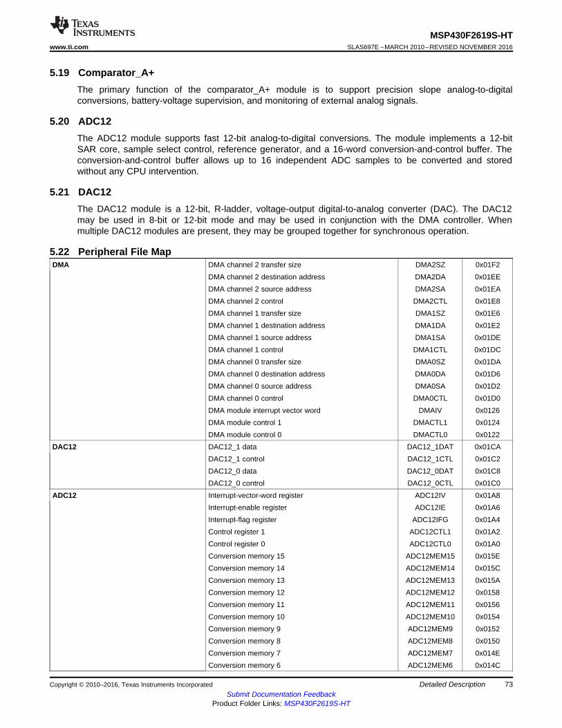
73
MSP430F2619S-HTwww.ti.com SLAS697E –MARCH 2010–REVISED NOVEMBER 2016
Submit Documentation FeedbackProduct Folder Links: MSP430F2619S-HT
Detailed DescriptionCopyright © 2010–2016, Texas Instruments Incorporated
5.19 Comparator_A+The primary function of the comparator_A+ module is to support precision slope analog-to-digitalconversions, battery-voltage supervision, and monitoring of external analog signals.
5.20 ADC12The ADC12 module supports fast 12-bit analog-to-digital conversions. The module implements a 12-bitSAR core, sample select control, reference generator, and a 16-word conversion-and-control buffer. Theconversion-and-control buffer allows up to 16 independent ADC samples to be converted and storedwithout any CPU intervention.
5.21 DAC12The DAC12 module is a 12-bit, R-ladder, voltage-output digital-to-analog converter (DAC). The DAC12may be used in 8-bit or 12-bit mode and may be used in conjunction with the DMA controller. Whenmultiple DAC12 modules are present, they may be grouped together for synchronous operation.
5.22 Peripheral File MapDMA DMA channel 2 transfer size DMA2SZ 0x01F2
DMA channel 2 destination address DMA2DA 0x01EEDMA channel 2 source address DMA2SA 0x01EADMA channel 2 control DMA2CTL 0x01E8DMA channel 1 transfer size DMA1SZ 0x01E6DMA channel 1 destination address DMA1DA 0x01E2DMA channel 1 source address DMA1SA 0x01DEDMA channel 1 control DMA1CTL 0x01DCDMA channel 0 transfer size DMA0SZ 0x01DADMA channel 0 destination address DMA0DA 0x01D6DMA channel 0 source address DMA0SA 0x01D2DMA channel 0 control DMA0CTL 0x01D0DMA module interrupt vector word DMAIV 0x0126DMA module control 1 DMACTL1 0x0124DMA module control 0 DMACTL0 0x0122
DAC12 DAC12_1 data DAC12_1DAT 0x01CADAC12_1 control DAC12_1CTL 0x01C2DAC12_0 data DAC12_0DAT 0x01C8DAC12_0 control DAC12_0CTL 0x01C0
ADC12 Interrupt-vector-word register ADC12IV 0x01A8Interrupt-enable register ADC12IE 0x01A6Interrupt-flag register ADC12IFG 0x01A4Control register 1 ADC12CTL1 0x01A2Control register 0 ADC12CTL0 0x01A0Conversion memory 15 ADC12MEM15 0x015EConversion memory 14 ADC12MEM14 0x015CConversion memory 13 ADC12MEM13 0x015AConversion memory 12 ADC12MEM12 0x0158Conversion memory 11 ADC12MEM11 0x0156Conversion memory 10 ADC12MEM10 0x0154Conversion memory 9 ADC12MEM9 0x0152Conversion memory 8 ADC12MEM8 0x0150Conversion memory 7 ADC12MEM7 0x014EConversion memory 6 ADC12MEM6 0x014C
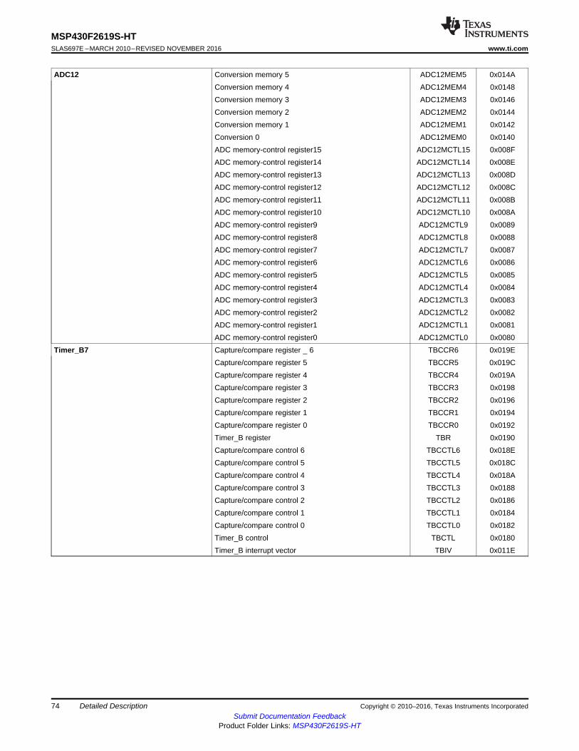
74
MSP430F2619S-HTSLAS697E –MARCH 2010–REVISED NOVEMBER 2016 www.ti.com
Submit Documentation FeedbackProduct Folder Links: MSP430F2619S-HT
Detailed Description Copyright © 2010–2016, Texas Instruments Incorporated
ADC12 Conversion memory 5 ADC12MEM5 0x014AConversion memory 4 ADC12MEM4 0x0148Conversion memory 3 ADC12MEM3 0x0146Conversion memory 2 ADC12MEM2 0x0144Conversion memory 1 ADC12MEM1 0x0142Conversion 0 ADC12MEM0 0x0140ADC memory-control register15 ADC12MCTL15 0x008FADC memory-control register14 ADC12MCTL14 0x008EADC memory-control register13 ADC12MCTL13 0x008DADC memory-control register12 ADC12MCTL12 0x008CADC memory-control register11 ADC12MCTL11 0x008BADC memory-control register10 ADC12MCTL10 0x008AADC memory-control register9 ADC12MCTL9 0x0089ADC memory-control register8 ADC12MCTL8 0x0088ADC memory-control register7 ADC12MCTL7 0x0087ADC memory-control register6 ADC12MCTL6 0x0086ADC memory-control register5 ADC12MCTL5 0x0085ADC memory-control register4 ADC12MCTL4 0x0084ADC memory-control register3 ADC12MCTL3 0x0083ADC memory-control register2 ADC12MCTL2 0x0082ADC memory-control register1 ADC12MCTL1 0x0081ADC memory-control register0 ADC12MCTL0 0x0080
Timer_B7 Capture/compare register _ 6 TBCCR6 0x019ECapture/compare register 5 TBCCR5 0x019CCapture/compare register 4 TBCCR4 0x019ACapture/compare register 3 TBCCR3 0x0198Capture/compare register 2 TBCCR2 0x0196Capture/compare register 1 TBCCR1 0x0194Capture/compare register 0 TBCCR0 0x0192Timer_B register TBR 0x0190Capture/compare control 6 TBCCTL6 0x018ECapture/compare control 5 TBCCTL5 0x018CCapture/compare control 4 TBCCTL4 0x018ACapture/compare control 3 TBCCTL3 0x0188Capture/compare control 2 TBCCTL2 0x0186Capture/compare control 1 TBCCTL1 0x0184Capture/compare control 0 TBCCTL0 0x0182Timer_B control TBCTL 0x0180Timer_B interrupt vector TBIV 0x011E
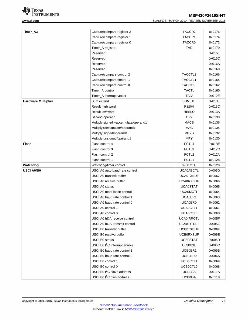
75
MSP430F2619S-HTwww.ti.com SLAS697E –MARCH 2010–REVISED NOVEMBER 2016
Submit Documentation FeedbackProduct Folder Links: MSP430F2619S-HT
Detailed DescriptionCopyright © 2010–2016, Texas Instruments Incorporated
Timer_A3 Capture/compare register 2 TACCR2 0x0176Capture/compare register 1 TACCR1 0x0174Capture/compare register 0 TACCR0 0x0172Timer_A register TAR 0x0170Reserved 0x016EReserved 0x016CReserved 0x016AReserved 0x0168Capture/compare control 2 TACCTL2 0x0166Capture/compare control 1 TACCTL1 0x0164Capture/compare control 0 TACCTL0 0x0162Timer_A control TACTL 0x0160Timer_A interrupt vector TAIV 0x012E
Hardware Multiplier Sum extend SUMEXT 0x013EResult high word RESHI 0x013CResult low word RESLO 0x013ASecond operand OP2 0x0138Multiply signed +accumulate/operand1 MACS 0x0136Multiply+accumulate/operand1 MAC 0x0134Multiply signed/operand1 MPYS 0x0132Multiply unsigned/operand1 MPY 0x0130
Flash Flash control 4 FCTL4 0x01BEFlash control 3 FCTL3 0x012CFlash control 2 FCTL2 0x012AFlash control 1 FCTL1 0x0128
Watchdog Watchdog/timer control WDTCTL 0x0120USCI A0/B0 USCI A0 auto baud rate control UCA0ABCTL 0x005D
USCI A0 transmit buffer UCA0TXBUF 0x0067USCI A0 receive buffer UCA0RXBUF 0x0066USCI A0 status UCA0STAT 0x0065USCI A0 modulation control UCA0MCTL 0x0064USCI A0 baud rate control 1 UCA0BR1 0x0063USCI A0 baud rate control 0 UCA0BR0 0x0062USCI A0 control 1 UCA0CTL1 0x0061USCI A0 control 0 UCA0CTL0 0x0060USCI A0 IrDA receive control UCA0IRRCTL 0x005FUSCI A0 IrDA transmit control UCA0IRTCLT 0x005EUSCI B0 transmit buffer UCB0TXBUF 0x006FUSCI B0 receive buffer UCB0RXBUF 0x006EUSCI B0 status UCB0STAT 0x006DUSCI B0 I2C interrupt enable UCB0CIE 0x006CUSCI B0 baud rate control 1 UCB0BR1 0x006BUSCI B0 baud rate control 0 UCB0BR0 0x006AUSCI B0 control 1 UCB0CTL1 0x0069USCI B0 control 0 UCB0CTL0 0x0068USCI B0 I2C slave address UCB0SA 0x011AUSCI B0 I2C own address UCB0OA 0x0118
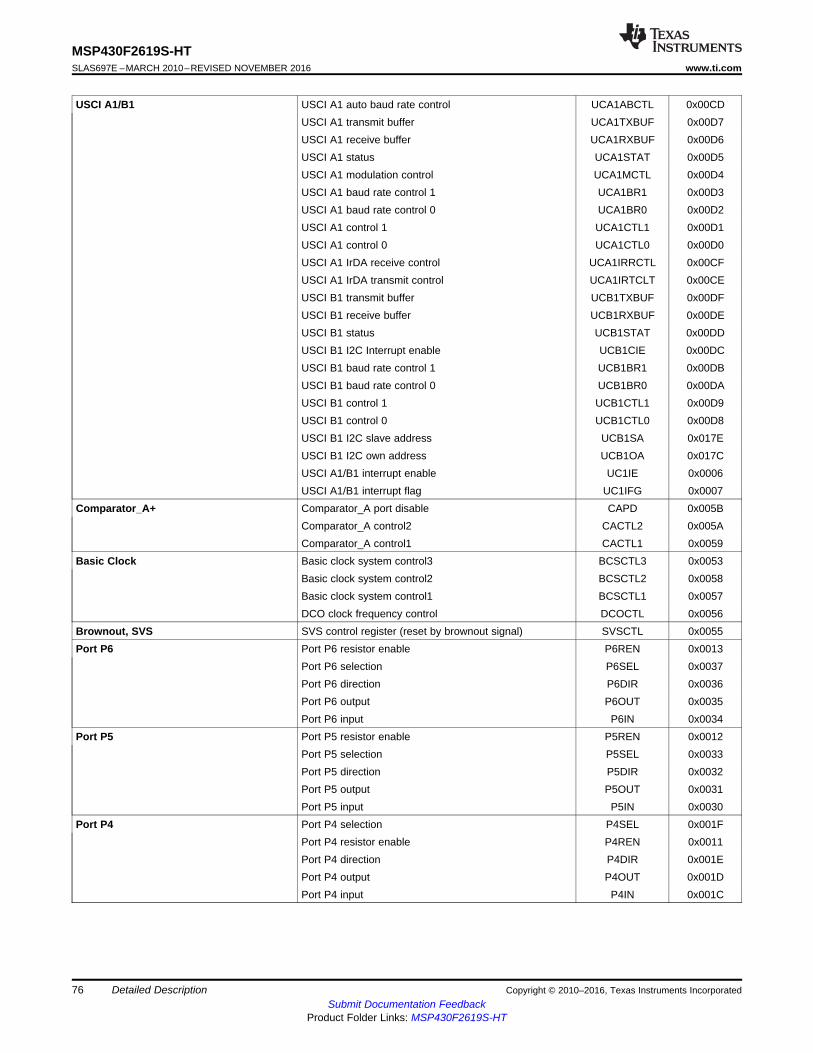
76
MSP430F2619S-HTSLAS697E –MARCH 2010–REVISED NOVEMBER 2016 www.ti.com
Submit Documentation FeedbackProduct Folder Links: MSP430F2619S-HT
Detailed Description Copyright © 2010–2016, Texas Instruments Incorporated
USCI A1/B1 USCI A1 auto baud rate control UCA1ABCTL 0x00CDUSCI A1 transmit buffer UCA1TXBUF 0x00D7USCI A1 receive buffer UCA1RXBUF 0x00D6USCI A1 status UCA1STAT 0x00D5USCI A1 modulation control UCA1MCTL 0x00D4USCI A1 baud rate control 1 UCA1BR1 0x00D3USCI A1 baud rate control 0 UCA1BR0 0x00D2USCI A1 control 1 UCA1CTL1 0x00D1USCI A1 control 0 UCA1CTL0 0x00D0USCI A1 IrDA receive control UCA1IRRCTL 0x00CFUSCI A1 IrDA transmit control UCA1IRTCLT 0x00CEUSCI B1 transmit buffer UCB1TXBUF 0x00DFUSCI B1 receive buffer UCB1RXBUF 0x00DEUSCI B1 status UCB1STAT 0x00DDUSCI B1 I2C Interrupt enable UCB1CIE 0x00DCUSCI B1 baud rate control 1 UCB1BR1 0x00DBUSCI B1 baud rate control 0 UCB1BR0 0x00DAUSCI B1 control 1 UCB1CTL1 0x00D9USCI B1 control 0 UCB1CTL0 0x00D8USCI B1 I2C slave address UCB1SA 0x017EUSCI B1 I2C own address UCB1OA 0x017CUSCI A1/B1 interrupt enable UC1IE 0x0006USCI A1/B1 interrupt flag UC1IFG 0x0007
Comparator_A+ Comparator_A port disable CAPD 0x005BComparator_A control2 CACTL2 0x005AComparator_A control1 CACTL1 0x0059
Basic Clock Basic clock system control3 BCSCTL3 0x0053Basic clock system control2 BCSCTL2 0x0058Basic clock system control1 BCSCTL1 0x0057DCO clock frequency control DCOCTL 0x0056
Brownout, SVS SVS control register (reset by brownout signal) SVSCTL 0x0055Port P6 Port P6 resistor enable P6REN 0x0013
Port P6 selection P6SEL 0x0037Port P6 direction P6DIR 0x0036Port P6 output P6OUT 0x0035Port P6 input P6IN 0x0034
Port P5 Port P5 resistor enable P5REN 0x0012Port P5 selection P5SEL 0x0033Port P5 direction P5DIR 0x0032Port P5 output P5OUT 0x0031Port P5 input P5IN 0x0030
Port P4 Port P4 selection P4SEL 0x001FPort P4 resistor enable P4REN 0x0011Port P4 direction P4DIR 0x001EPort P4 output P4OUT 0x001DPort P4 input P4IN 0x001C
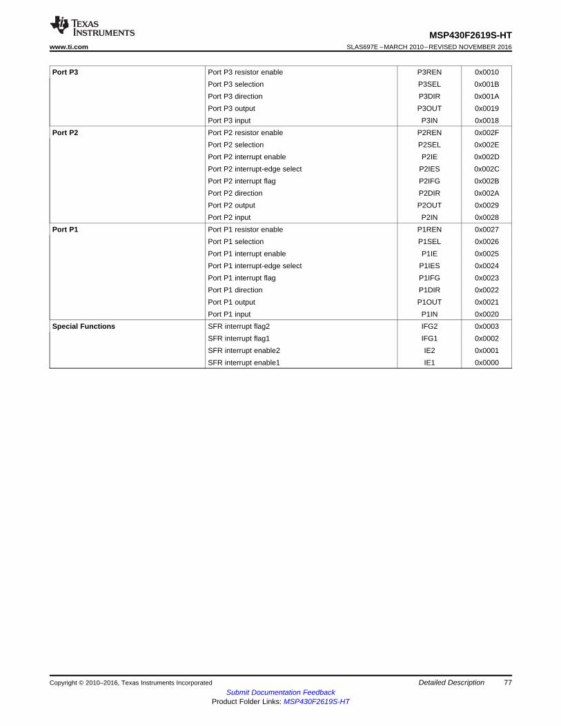
77
MSP430F2619S-HTwww.ti.com SLAS697E –MARCH 2010–REVISED NOVEMBER 2016
Submit Documentation FeedbackProduct Folder Links: MSP430F2619S-HT
Detailed DescriptionCopyright © 2010–2016, Texas Instruments Incorporated
Port P3 Port P3 resistor enable P3REN 0x0010Port P3 selection P3SEL 0x001BPort P3 direction P3DIR 0x001APort P3 output P3OUT 0x0019Port P3 input P3IN 0x0018
Port P2 Port P2 resistor enable P2REN 0x002FPort P2 selection P2SEL 0x002EPort P2 interrupt enable P2IE 0x002DPort P2 interrupt-edge select P2IES 0x002CPort P2 interrupt flag P2IFG 0x002BPort P2 direction P2DIR 0x002APort P2 output P2OUT 0x0029Port P2 input P2IN 0x0028
Port P1 Port P1 resistor enable P1REN 0x0027Port P1 selection P1SEL 0x0026Port P1 interrupt enable P1IE 0x0025Port P1 interrupt-edge select P1IES 0x0024Port P1 interrupt flag P1IFG 0x0023Port P1 direction P1DIR 0x0022Port P1 output P1OUT 0x0021Port P1 input P1IN 0x0020
Special Functions SFR interrupt flag2 IFG2 0x0003SFR interrupt flag1 IFG1 0x0002SFR interrupt enable2 IE2 0x0001SFR interrupt enable1 IE1 0x0000
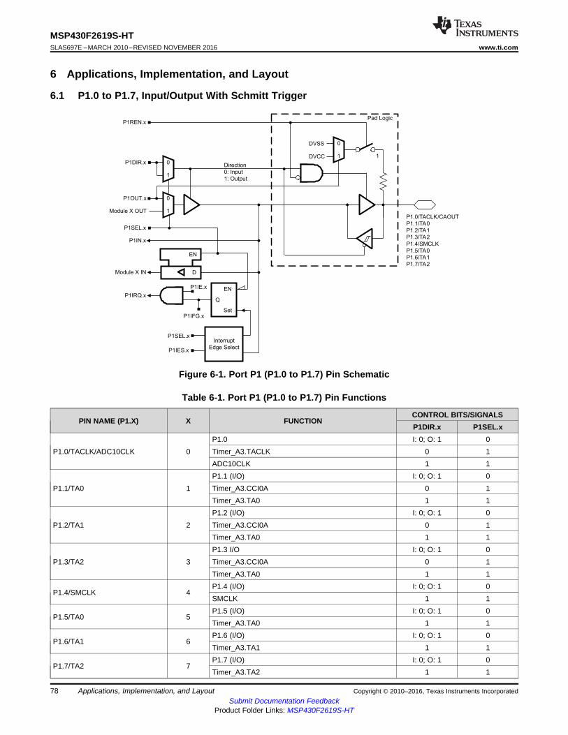
Direction
0: Input
1: Output
P1SEL.x
P1DIR.x
P1IN.x
P1IRQ.x
D
EN
Module X IN
Module X OUT
P1OUT.x
Interrupt
Edge Select
Q
EN
Set
P1SEL.x
P1IES.x
P1IFG.x
P1IE.x
P1.0/TACLK/CAOUT
P1.1/TA0
P1.2/TA1
P1.3/TA2
P1.4/SMCLK
P1.5/TA0
P1.6/TA1
P1.7/TA2
DVSS
DVCC
Pad Logic
1
1
0
1
0
1
0
P1REN.x
78
MSP430F2619S-HTSLAS697E –MARCH 2010–REVISED NOVEMBER 2016 www.ti.com
Submit Documentation FeedbackProduct Folder Links: MSP430F2619S-HT
Applications, Implementation, and Layout Copyright © 2010–2016, Texas Instruments Incorporated
6 Applications, Implementation, and Layout
6.1 P1.0 to P1.7, Input/Output With Schmitt Trigger
Figure 6-1. Port P1 (P1.0 to P1.7) Pin Schematic
Table 6-1. Port P1 (P1.0 to P1.7) Pin Functions
PIN NAME (P1.X) X FUNCTIONCONTROL BITS/SIGNALSP1DIR.x P1SEL.x
P1.0/TACLK/ADC10CLK 0P1.0 I: 0; O: 1 0Timer_A3.TACLK 0 1ADC10CLK 1 1
P1.1/TA0 1P1.1 (I/O) I: 0; O: 1 0Timer_A3.CCI0A 0 1Timer_A3.TA0 1 1
P1.2/TA1 2P1.2 (I/O) I: 0; O: 1 0Timer_A3.CCI0A 0 1Timer_A3.TA0 1 1
P1.3/TA2 3P1.3 I/O I: 0; O: 1 0Timer_A3.CCI0A 0 1Timer_A3.TA0 1 1
P1.4/SMCLK 4P1.4 (I/O) I: 0; O: 1 0SMCLK 1 1
P1.5/TA0 5P1.5 (I/O) I: 0; O: 1 0Timer_A3.TA0 1 1
P1.6/TA1 6P1.6 (I/O) I: 0; O: 1 0Timer_A3.TA1 1 1
P1.7/TA2 7P1.7 (I/O) I: 0; O: 1 0Timer_A3.TA2 1 1
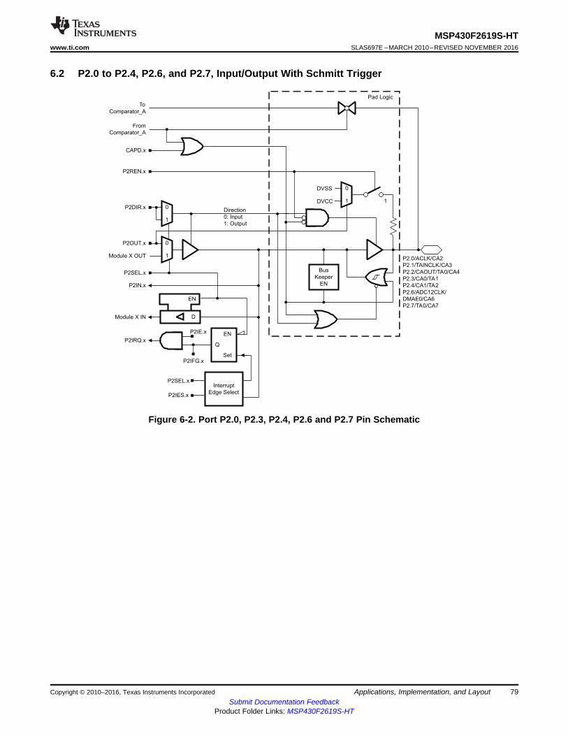
P2.0/ACLK/CA2
P2.1/TAINCLK/CA3
P2.2/CAOUT/TA0/CA4
P2.3/CA0/TA1
P2.4/CA1/TA2
P2.6/ADC12CLK/
DMAE0/CA6
P2.7/TA0/CA7
Direction
0: Input
1: Output
P2SEL.x
P2DIR.x
P2IN.x
P2IRQ.x
D
EN
Module X IN
Module X OUT
P2OUT.x
Interrupt
Edge Select
Q
EN
Set
P2SEL.x
P2IES.x
P2IFG.x
P2IE.x
DVSS
DVCC
P2REN.x
Pad Logic
1
1
0
1
0
1
0
Bus
Keeper
EN
CAPD.x
From
Comparator_A
To
Comparator_A
79
MSP430F2619S-HTwww.ti.com SLAS697E –MARCH 2010–REVISED NOVEMBER 2016
Submit Documentation FeedbackProduct Folder Links: MSP430F2619S-HT
Applications, Implementation, and LayoutCopyright © 2010–2016, Texas Instruments Incorporated
6.2 P2.0 to P2.4, P2.6, and P2.7, Input/Output With Schmitt Trigger
Figure 6-2. Port P2.0, P2.3, P2.4, P2.6 and P2.7 Pin Schematic
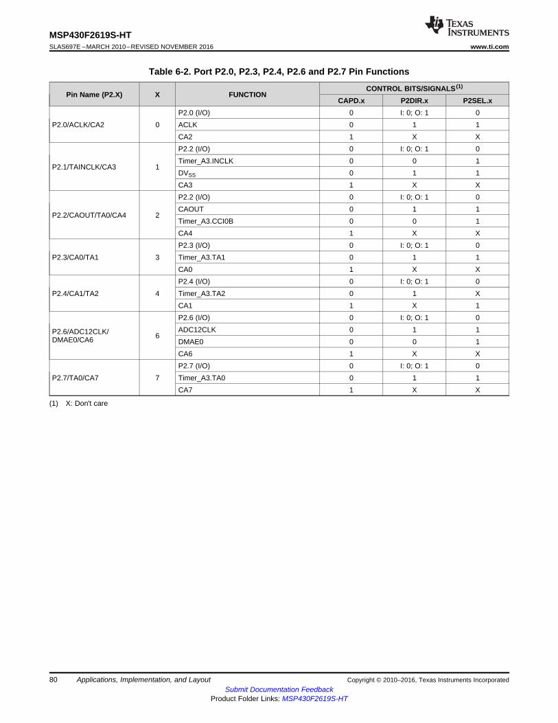
80
MSP430F2619S-HTSLAS697E –MARCH 2010–REVISED NOVEMBER 2016 www.ti.com
Submit Documentation FeedbackProduct Folder Links: MSP430F2619S-HT
Applications, Implementation, and Layout Copyright © 2010–2016, Texas Instruments Incorporated
(1) X: Don't care
Table 6-2. Port P2.0, P2.3, P2.4, P2.6 and P2.7 Pin Functions
Pin Name (P2.X) X FUNCTIONCONTROL BITS/SIGNALS (1)
CAPD.x P2DIR.x P2SEL.x
P2.0/ACLK/CA2 0P2.0 (I/O) 0 I: 0; O: 1 0ACLK 0 1 1CA2 1 X X
P2.1/TAINCLK/CA3 1
P2.2 (I/O) 0 I: 0; O: 1 0Timer_A3.INCLK 0 0 1DVSS 0 1 1CA3 1 X X
P2.2/CAOUT/TA0/CA4 2
P2.2 (I/O) 0 I: 0; O: 1 0CAOUT 0 1 1Timer_A3.CCI0B 0 0 1CA4 1 X X
P2.3/CA0/TA1 3P2.3 (I/O) 0 I: 0; O: 1 0Timer_A3.TA1 0 1 1CA0 1 X X
P2.4/CA1/TA2 4P2.4 (I/O) 0 I: 0; O: 1 0Timer_A3.TA2 0 1 XCA1 1 X 1
P2.6/ADC12CLK/DMAE0/CA6 6
P2.6 (I/O) 0 I: 0; O: 1 0ADC12CLK 0 1 1DMAE0 0 0 1CA6 1 X X
P2.7/TA0/CA7 7P2.7 (I/O) 0 I: 0; O: 1 0Timer_A3.TA0 0 1 1CA7 1 X X
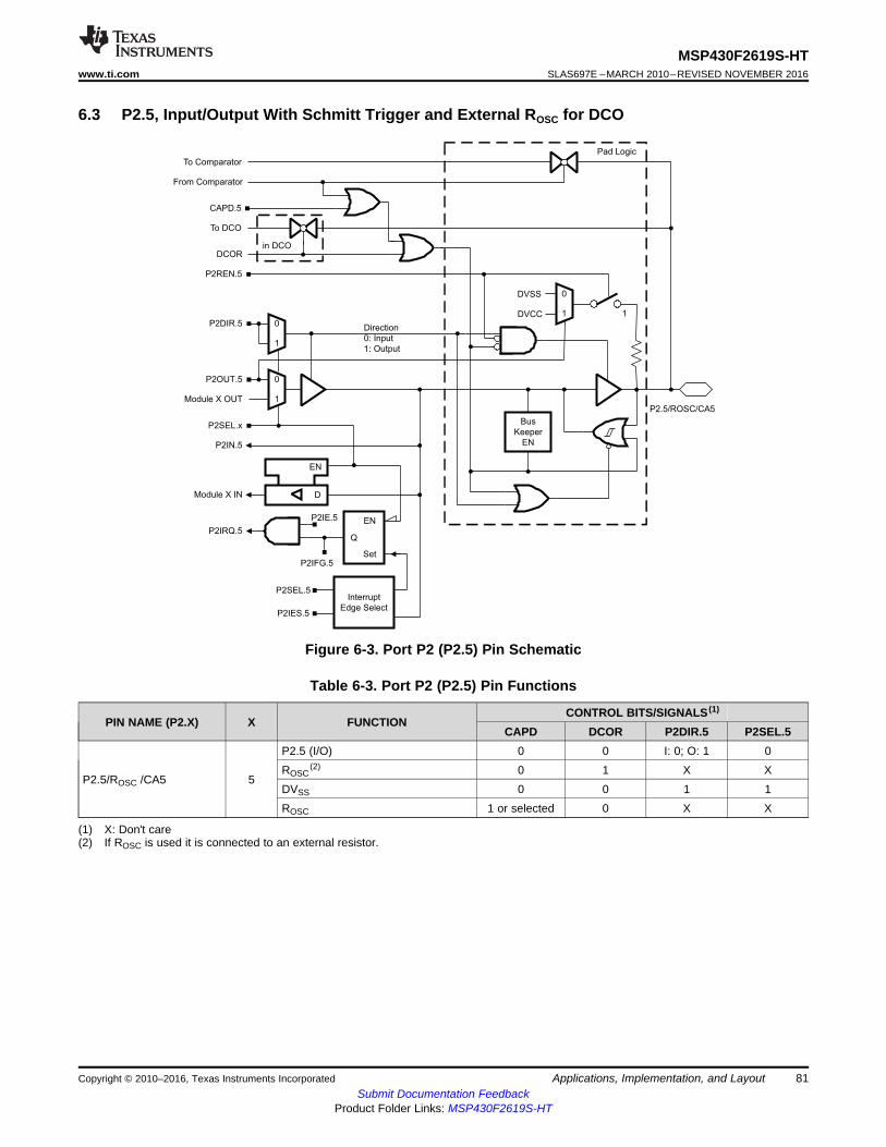
Direction
0: Input
1: Output
P2SEL.x
P2DIR.5
P2IN.5
P2IRQ.5
D
EN
Module X IN
Module X OUT
P2OUT.5
Interrupt
Edge Select
Q
EN
Set
P2SEL.5
P2IES.5
P2IFG.5
P2IE.5
P2.5/ROSC/CA5
DVSS
DVCC 1
1
0
1
0
1
0
Bus
Keeper
EN
DCOR
To DCO
Pad Logic
From Comparator
To Comparator
CAPD.5
in DCO
P2REN.5
81
MSP430F2619S-HTwww.ti.com SLAS697E –MARCH 2010–REVISED NOVEMBER 2016
Submit Documentation FeedbackProduct Folder Links: MSP430F2619S-HT
Applications, Implementation, and LayoutCopyright © 2010–2016, Texas Instruments Incorporated
(1) X: Don't care(2) If ROSC is used it is connected to an external resistor.
6.3 P2.5, Input/Output With Schmitt Trigger and External ROSC for DCO
Figure 6-3. Port P2 (P2.5) Pin Schematic
Table 6-3. Port P2 (P2.5) Pin Functions
PIN NAME (P2.X) X FUNCTIONCONTROL BITS/SIGNALS (1)
CAPD DCOR P2DIR.5 P2SEL.5
P2.5/ROSC /CA5 5
P2.5 (I/O) 0 0 I: 0; O: 1 0ROSC
(2) 0 1 X XDVSS 0 0 1 1ROSC 1 or selected 0 X X
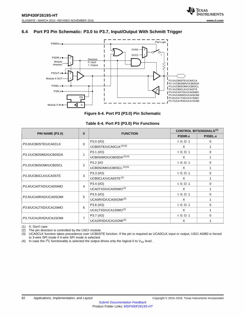
Direction
0: Input
1: Output
P3SEL.x
P3DIR.x
P3IN.x
D
EN
Module X IN
Module X OUT
P3OUT.x
DVSS
DVCC
Pad Logic
1
1
0
1
0
1
0
P3.0/UCB0STE/UCA0CLK
P3.1/UCB0SIMO/UCB0SDA
P3.2/UCB0SOMI/UCB0SCL
P3.3/UCB0CLK/UCA0STE
P3.4/UCA0TXD/UCA0SIMO
P3.5/UCA0RXD/UCA0SOMI
P3.6/UCA1TXD/UCA1SIMO
P3.7/UCA1RXD/UCA1SOMI
P3REN.x
Module
direction
82
MSP430F2619S-HTSLAS697E –MARCH 2010–REVISED NOVEMBER 2016 www.ti.com
Submit Documentation FeedbackProduct Folder Links: MSP430F2619S-HT
Applications, Implementation, and Layout Copyright © 2010–2016, Texas Instruments Incorporated
(1) X: Don’t care(2) The pin direction is controlled by the USCI module.(3) UCA0CLK function takes precedence over UCB0STE function. If the pin is required as UCA0CLK input or output, USCI A0/B0 is forced
to 3-wire SPI mode if 4-wire SPI mode is selected.(4) In case the I2C functionality is selected the output drives only the logical 0 to VSS level.
6.4 Port P3 Pin Schematic: P3.0 to P3.7, Input/Output With Schmitt Trigger
Figure 6-4. Port P3 (P3.0) Pin Schematic
Table 6-4. Port P3 (P3.0) Pin Functions
PIN NAME (P3.X) X FUNCTIONCONTROL BITS/SIGNALS (1)
P3DIR.x P3SEL.x
P3.0/UCB0STE/UCA0CLK 0P3.0 (I/O) I: 0; O: 1 0UCB0STE/UCA0CLK (2) (3) X 1
P3.1/UCB0SIMO/UCB0SDA 1P3.1 (I/O) I: 0; O: 1 0UCB0SIMO/UCB0SDA (2) (4) X 1
P3.2/UCB0SOMI/UCB0SCL 2P3.2 (I/O I: 0; O: 1 0UCB0SOMI/UCB0SCL (2) (4) X 1
P3.3/UCB0CLK/UCA0STE 3P3.3 (I/O) I: 0; O: 1 0UCB0CLK/UCA0STE (2) X 1
P3.4/UCA0TXD/UCA0SIMO 4P3.4 (I/O) I: 0; O: 1 0UCA0TXD/UCA0SIMO (2) X 1
P3.5/UCA0RXD/UCA0SOMI 5P3.5 (I/O) I: 0; O: 1 0UCA0RXD/UCA0SOMI (2) X 1
P3.6/UCA1TXD/UCA1SIMO 6P3.6 (I/O) I: 0; O: 1 0UCA1TXD/UCA1SIMO (2) X 1
P3.7/UCA1RXD/UCA1SOMI 7P3.7 (I/O) I: 0; O: 1 0UCA1RXD/UCA1SOMI (2) X 1
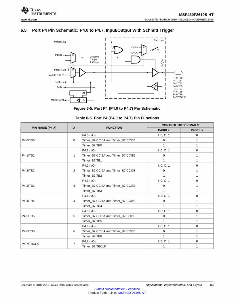
P4.0/TB0
P4.1/TB1
P4.2/TB2
P4.3/TB3
P4.4/TB4
P4.5/TB5
P4.6/TB6
P4.7/TBCLK
P4SEL.x
P4DIR.x
P4IN.x
Module X IN
Module X OUT
P4OUT.x
P4REN.x
Direction
0: Input
1: Output
D
EN
DVSS
DVCC
Pad Logic
1
1
0
1
0
1
0
83
MSP430F2619S-HTwww.ti.com SLAS697E –MARCH 2010–REVISED NOVEMBER 2016
Submit Documentation FeedbackProduct Folder Links: MSP430F2619S-HT
Applications, Implementation, and LayoutCopyright © 2010–2016, Texas Instruments Incorporated
6.5 Port P4 Pin Schematic: P4.0 to P4.7, Input/Output With Schmitt Trigger
Figure 6-5. Port P4 (P4.0 to P4.7) Pin Schematic
Table 6-5. Port P4 (P4.0 to P4.7) Pin Functions
PIN NAME (P4.X) X FUNCTIONCONTROL BITS/SIGNALS
P4DIR.x P4SEL.x
P4.0/TB0 0P4.0 (I/O) I: 0; O: 1 0Timer_B7.CCI0A and Timer_B7.CCI0B 0 1Timer_B7.TB0 1 1
P4.1/TB1 1P4.1 (I/O) I: 0; O: 1 0Timer_B7.CCI1A and Timer_B7.CCI1B 0 1Timer_B7.TB1 1 1
P4.2/TB2 2P4.2 (I/O) I: 0; O: 1 0Timer_B7.CCI2A and Timer_B7.CCI2B 0 1Timer_B7.TB2 1 1
P4.3/TB3 3P4.3 (I/O) I: 0; O: 1 0Timer_B7.CCI3A and Timer_B7.CCI3B 0 1Timer_B7.TB3 1 1
P4.4/TB4 4P4.4 (I/O) I: 0; O: 1 0Timer_B7.CCI4A and Timer_B7.CCI4B 0 1Timer_B7.TB4 1 1
P4.5/TB5 5P4.5 (I/O) I: 0; O: 1 0Timer_B7.CCI5A and Timer_B7.CCI5B 0 1Timer_B7.TB5 1 1
P4.6/TB6 6P4.6 (I/O) I: 0; O: 1 0Timer_B7.CCI6A and Timer_B7.CCI6B 0 1Timer_B7.TB6 1 1
P4.7/TBCLK 7P4.7 (I/O) I: 0; O: 1 0Timer_B7.TBCLK 1 1
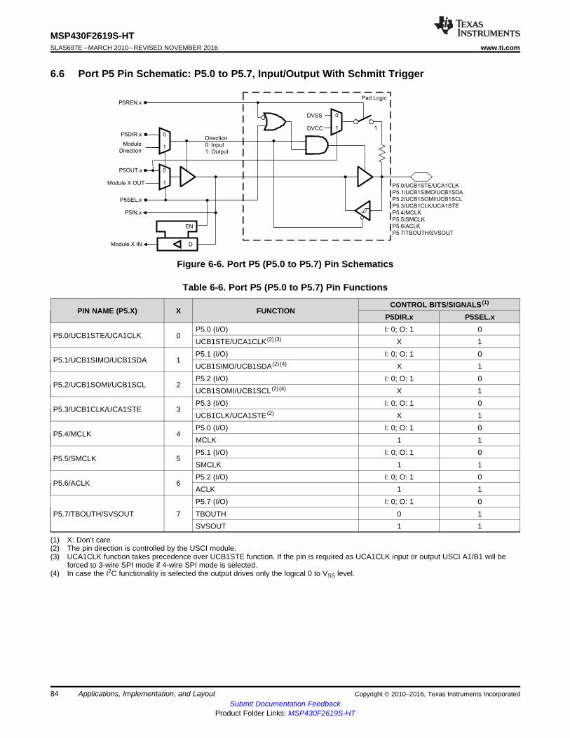
P5SEL.x
P5DIR.x
P5IN.x
Module X IN
Module X OUT
P5OUT.x
P5REN.x
P5.0/UCB1STE/UCA1CLK
P5.1/UCB1SIMO/UCB1SDA
P5.2/UCB1SOMI/UCB1SCL
P5.3/UCB1CLK/UCA1STE
P5.4/MCLK
P5.5/SMCLK
P5.6/ACLK
P5.7/TBOUTH/SVSOUT
Module
Direction
Direction
0: Input
1: Output
D
EN
DVSS
DVCC
Pad Logic
1
1
0
1
0
1
0
84
MSP430F2619S-HTSLAS697E –MARCH 2010–REVISED NOVEMBER 2016 www.ti.com
Submit Documentation FeedbackProduct Folder Links: MSP430F2619S-HT
Applications, Implementation, and Layout Copyright © 2010–2016, Texas Instruments Incorporated
(1) X: Don’t care(2) The pin direction is controlled by the USCI module.(3) UCA1CLK function takes precedence over UCB1STE function. If the pin is required as UCA1CLK input or output USCI A1/B1 will be
forced to 3-wire SPI mode if 4-wire SPI mode is selected.(4) In case the I2C functionality is selected the output drives only the logical 0 to VSS level.
6.6 Port P5 Pin Schematic: P5.0 to P5.7, Input/Output With Schmitt Trigger
Figure 6-6. Port P5 (P5.0 to P5.7) Pin Schematics
Table 6-6. Port P5 (P5.0 to P5.7) Pin Functions
PIN NAME (P5.X) X FUNCTIONCONTROL BITS/SIGNALS (1)
P5DIR.x P5SEL.x
P5.0/UCB1STE/UCA1CLK 0P5.0 (I/O) I: 0; O: 1 0UCB1STE/UCA1CLK (2) (3) X 1
P5.1/UCB1SIMO/UCB1SDA 1P5.1 (I/O) I: 0; O: 1 0UCB1SIMO/UCB1SDA (2) (4) X 1
P5.2/UCB1SOMI/UCB1SCL 2P5.2 (I/O) I: 0; O: 1 0UCB1SOMI/UCB1SCL (2) (4) X 1
P5.3/UCB1CLK/UCA1STE 3P5.3 (I/O) I: 0; O: 1 0UCB1CLK/UCA1STE (2) X 1
P5.4/MCLK 4P5.0 (I/O) I: 0; O: 1 0MCLK 1 1
P5.5/SMCLK 5P5.1 (I/O) I: 0; O: 1 0SMCLK 1 1
P5.6/ACLK 6P5.2 (I/O) I: 0; O: 1 0ACLK 1 1
P5.7/TBOUTH/SVSOUT 7P5.7 (I/O) I: 0; O: 1 0TBOUTH 0 1SVSOUT 1 1
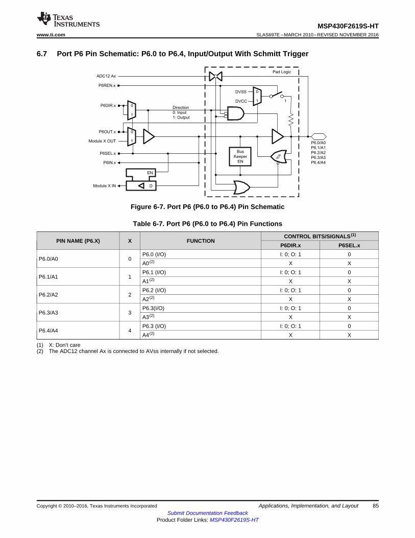
Direction
0: Input
1: Output
P6SEL.x
P6DIR.x
P6IN.x
D
EN
Module X IN
Module X OUT
P6OUT.x
P6.0/A0
P6.1/A1
P6.2/A2
P6.3/A3
P6.4/A4
DVSS
DVCC
Pad Logic
1
1
0
1
0
1
0
Bus
Keeper
EN
ADC12 Ax
P6REN.x
85
MSP430F2619S-HTwww.ti.com SLAS697E –MARCH 2010–REVISED NOVEMBER 2016
Submit Documentation FeedbackProduct Folder Links: MSP430F2619S-HT
Applications, Implementation, and LayoutCopyright © 2010–2016, Texas Instruments Incorporated
(1) X: Don’t care(2) The ADC12 channel Ax is connected to AVss internally if not selected.
6.7 Port P6 Pin Schematic: P6.0 to P6.4, Input/Output With Schmitt Trigger
Figure 6-7. Port P6 (P6.0 to P6.4) Pin Schematic
Table 6-7. Port P6 (P6.0 to P6.4) Pin Functions
PIN NAME (P6.X) X FUNCTIONCONTROL BITS/SIGNALS (1)
P6DIR.x P6SEL.x
P6.0/A0 0P6.0 (I/O) I: 0; O: 1 0A0 (2) X X
P6.1/A1 1P6.1 (I/O) I: 0; O: 1 0A1 (2) X X
P6.2/A2 2P6.2 (I/O) I: 0; O: 1 0A2 (2) X X
P6.3/A3 3P6.3(I/O) I: 0; O: 1 0A3 (2) X X
P6.4/A4 4P6.3 (I/O) I: 0; O: 1 0A4 (2) X X
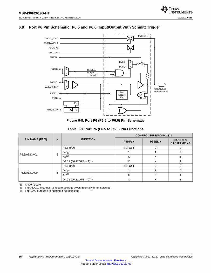
P6.5/A5/DAC1
P6.6/A6/DAC0
Direction
0: Input
1: Output
P6SEL.x
P6DIR.x
P6IN.x
D
EN
Module X IN
Module X OUT
P6OUT.x
DVSS
DVCC
P6REN.x
Pad Logic
1
1
0
1
0
1
0
Bus
Keeper
EN
ADC12 Ax
DAC12AMP > 0
DAC12_0OUT
ADC12 Ax
86
MSP430F2619S-HTSLAS697E –MARCH 2010–REVISED NOVEMBER 2016 www.ti.com
Submit Documentation FeedbackProduct Folder Links: MSP430F2619S-HT
Applications, Implementation, and Layout Copyright © 2010–2016, Texas Instruments Incorporated
(1) X: Don’t care(2) The ADC12 channel Ax is connected to AVss internally if not selected.(3) The DAC outputs are floating if not selected.
6.8 Port P6 Pin Schematic: P6.5 and P6.6, Input/Output With Schmitt Trigger
Figure 6-8. Port P6 (P6.5 to P6.6) Pin Schematic
Table 6-8. Port P6 (P6.5 to P6.6) Pin Functions
PIN NAME (P6.X) X FUNCTIONCONTROL BITS/SIGNALS (1)
P6DIR.x P6SEL.x CAPD.x orDAC12AMP > 0
P6.5/A5/DAC1 5
P6.5 (I/O) I: 0; O: 1 0 0DVSS 1 1 0A5 (2) X X 1DAC1 (DA12OPS = 1) (3) X X 1
P6.6/A6/DAC0 6
P6.6 (I/O) I: 0; O: 1 0 0DVSS 1 1 0A6 (2) X X 1DAC1 (DA12OPS = 0) (3) X X 1
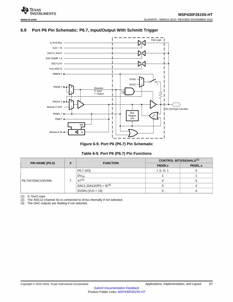
Direction
0: Input
1: Output
P6SEL.7
P6DIR.7
P6IN.7
D
EN
Module X IN
Module X OUT
P6OUT.7
P6.7/A7/DAC1/SVSIN
DVSS
DVCC
P6REN.7
Pad Logic
1
1
0
1
0
1
0
Bus
Keeper
EN
ADC12 A7
DAC12AMP > 0
DAC12_0OUT
VLD = 15
to SVS Mux
from ADC12
87
MSP430F2619S-HTwww.ti.com SLAS697E –MARCH 2010–REVISED NOVEMBER 2016
Submit Documentation FeedbackProduct Folder Links: MSP430F2619S-HT
Applications, Implementation, and LayoutCopyright © 2010–2016, Texas Instruments Incorporated
(1) X: Don’t care(2) The ADC12 channel Ax is connected to AVss internally if not selected.(3) The DAC outputs are floating if not selected.
6.9 Port P6 Pin Schematic: P6.7, Input/Output With Schmitt Trigger
Figure 6-9. Port P6 (P6.7) Pin Schematic
Table 6-9. Port P6 (P6.7) Pin Functions
PIN NAME (P6.X) X FUNCTIONCONTROL BITS/SIGNALS (1)
P6DIR.x P6SEL.x
P6.7/A7/DAC1/SVSIN 7
P6.7 (I/O) I: 0; O: 1 0DVSS 1 1A7 (2) X XDAC1 (DA12OPS = 0) (3) X XSVSIN (VLD = 15) X X
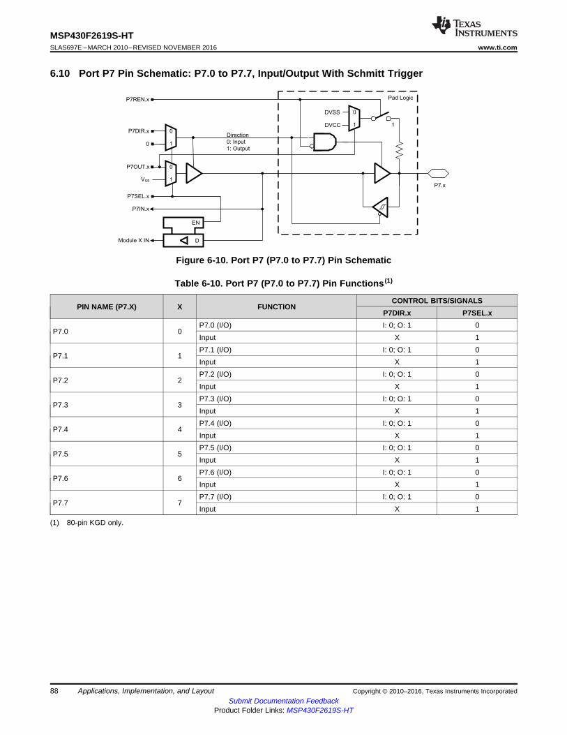
Direction
0: Input
1: Output
P7SEL.x
P7DIR.x
P7IN.x
D
EN
Module X IN
VSS
P7OUT.x
P7.x
DVSS
DVCC
P7REN.x Pad Logic
1
1
0
1
0
1
0
0
88
MSP430F2619S-HTSLAS697E –MARCH 2010–REVISED NOVEMBER 2016 www.ti.com
Submit Documentation FeedbackProduct Folder Links: MSP430F2619S-HT
Applications, Implementation, and Layout Copyright © 2010–2016, Texas Instruments Incorporated
(1) 80-pin KGD only.
6.10 Port P7 Pin Schematic: P7.0 to P7.7, Input/Output With Schmitt Trigger
Figure 6-10. Port P7 (P7.0 to P7.7) Pin Schematic
Table 6-10. Port P7 (P7.0 to P7.7) Pin Functions (1)
PIN NAME (P7.X) X FUNCTIONCONTROL BITS/SIGNALS
P7DIR.x P7SEL.x
P7.0 0P7.0 (I/O) I: 0; O: 1 0Input X 1
P7.1 1P7.1 (I/O) I: 0; O: 1 0Input X 1
P7.2 2P7.2 (I/O) I: 0; O: 1 0Input X 1
P7.3 3P7.3 (I/O) I: 0; O: 1 0Input X 1
P7.4 4P7.4 (I/O) I: 0; O: 1 0Input X 1
P7.5 5P7.5 (I/O) I: 0; O: 1 0Input X 1
P7.6 6P7.6 (I/O) I: 0; O: 1 0Input X 1
P7.7 7P7.7 (I/O) I: 0; O: 1 0Input X 1
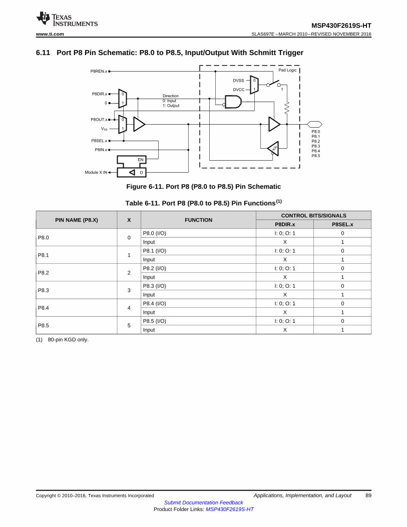
Direction
0: Input
1: Output
P8SEL.x
P8DIR.x
P8IN.x
D
EN
Module X IN
VSS
P8OUT.x
P8.0
P8.1
P8.2
P8.3
P8.4
P8.5
DVSS
DVCC
P8REN.x Pad Logic
1
1
0
1
0
1
0
0
89
MSP430F2619S-HTwww.ti.com SLAS697E –MARCH 2010–REVISED NOVEMBER 2016
Submit Documentation FeedbackProduct Folder Links: MSP430F2619S-HT
Applications, Implementation, and LayoutCopyright © 2010–2016, Texas Instruments Incorporated
(1) 80-pin KGD only.
6.11 Port P8 Pin Schematic: P8.0 to P8.5, Input/Output With Schmitt Trigger
Figure 6-11. Port P8 (P8.0 to P8.5) Pin Schematic
Table 6-11. Port P8 (P8.0 to P8.5) Pin Functions (1)
PIN NAME (P8.X) X FUNCTIONCONTROL BITS/SIGNALS
P8DIR.x P8SEL.x
P8.0 0P8.0 (I/O) I: 0; O: 1 0Input X 1
P8.1 1P8.1 (I/O) I: 0; O: 1 0Input X 1
P8.2 2P8.2 (I/O) I: 0; O: 1 0Input X 1
P8.3 3P8.3 (I/O) I: 0; O: 1 0Input X 1
P8.4 4P8.4 (I/O) I: 0; O: 1 0Input X 1
P8.5 5P8.5 (I/O) I: 0; O: 1 0Input X 1
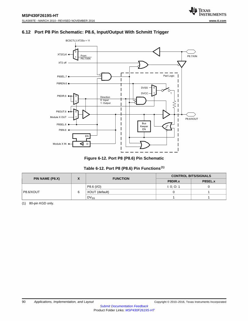
Direction
0: Input
1: Output
P8SEL.6
P8DIR.6
P8IN.6
D
EN
Module X IN
Module X OUT
P8OUT.6
DVSS
DVCC
Pad Logic
1
1
0
1
0
1
0
Bus
Keeper
EN
P8.6/XOUT
P8.7/XIN
P8SEL.7
P8REN.6
1
0XT2CLK
XT2 off
BCSCTL3.XT2Sx = 11
From
P8.7/XIN
90
MSP430F2619S-HTSLAS697E –MARCH 2010–REVISED NOVEMBER 2016 www.ti.com
Submit Documentation FeedbackProduct Folder Links: MSP430F2619S-HT
Applications, Implementation, and Layout Copyright © 2010–2016, Texas Instruments Incorporated
(1) 80-pin KGD only.
6.12 Port P8 Pin Schematic: P8.6, Input/Output With Schmitt Trigger
Figure 6-12. Port P8 (P8.6) Pin Schematic
Table 6-12. Port P8 (P8.6) Pin Functions (1)
PIN NAME (P8.X) X FUNCTIONCONTROL BITS/SIGNALS
P8DIR.x P8SEL.x
P8.6/XOUT 6P8.6 (I/O) I: 0; O: 1 0XOUT (default) 0 1DVSS 1 1
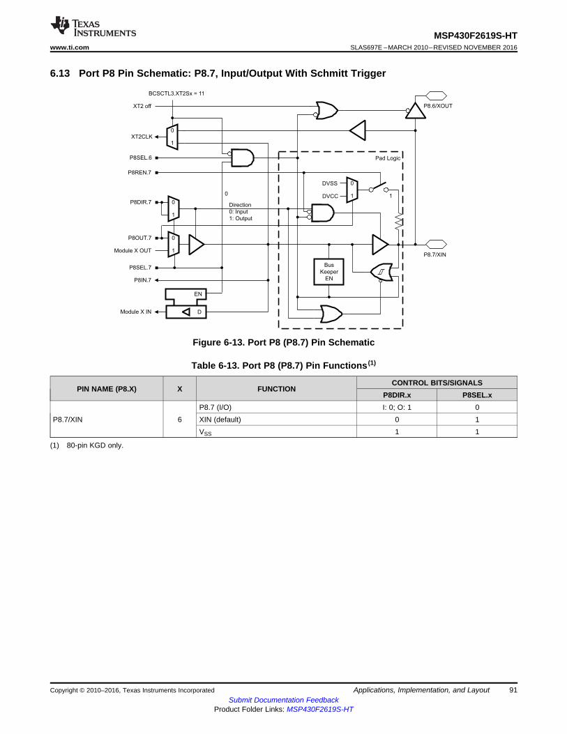
Direction
0: Input
1: Output
P8SEL.7
P8DIR.7
P8IN.7
D
EN
Module X IN
Module X OUT
P8OUT.7
DVSS
DVCC
Pad Logic
1
1
0
1
0
1
0
Bus
Keeper
EN
P8SEL.6
P8.7/XIN
1
0XT2CLK
0
P8.6/XOUTXT2 off
BCSCTL3.XT2Sx = 11
P8REN.7
91
MSP430F2619S-HTwww.ti.com SLAS697E –MARCH 2010–REVISED NOVEMBER 2016
Submit Documentation FeedbackProduct Folder Links: MSP430F2619S-HT
Applications, Implementation, and LayoutCopyright © 2010–2016, Texas Instruments Incorporated
(1) 80-pin KGD only.
6.13 Port P8 Pin Schematic: P8.7, Input/Output With Schmitt Trigger
Figure 6-13. Port P8 (P8.7) Pin Schematic
Table 6-13. Port P8 (P8.7) Pin Functions (1)
PIN NAME (P8.X) X FUNCTIONCONTROL BITS/SIGNALS
P8DIR.x P8SEL.x
P8.7/XIN 6P8.7 (I/O) I: 0; O: 1 0XIN (default) 0 1VSS 1 1
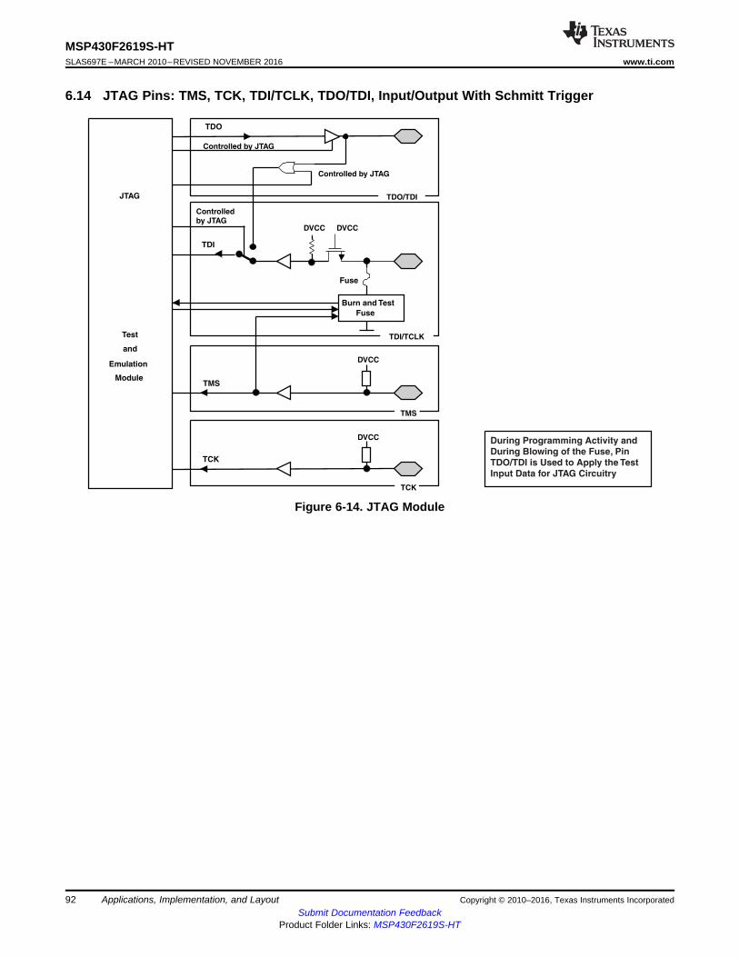
TDI
TDO
TMS
TCK
Test
JTAG
and
Emulation
Module
Burn and Test
Fuse
Controlled by JTAG
Controlled by JTAG
Controlledby JTAG
DVCC
DVCC
DVCC
TDO/TDI
TDI/TCLK
TMS
TCK
Fuse
DVCC
During Programming Activity andDuring Blowing of the Fuse, PinTDO/TDI is Used to Apply the TestInput Data for JTAG Circuitry
92
MSP430F2619S-HTSLAS697E –MARCH 2010–REVISED NOVEMBER 2016 www.ti.com
Submit Documentation FeedbackProduct Folder Links: MSP430F2619S-HT
Applications, Implementation, and Layout Copyright © 2010–2016, Texas Instruments Incorporated
6.14 JTAG Pins: TMS, TCK, TDI/TCLK, TDO/TDI, Input/Output With Schmitt Trigger
Figure 6-14. JTAG Module
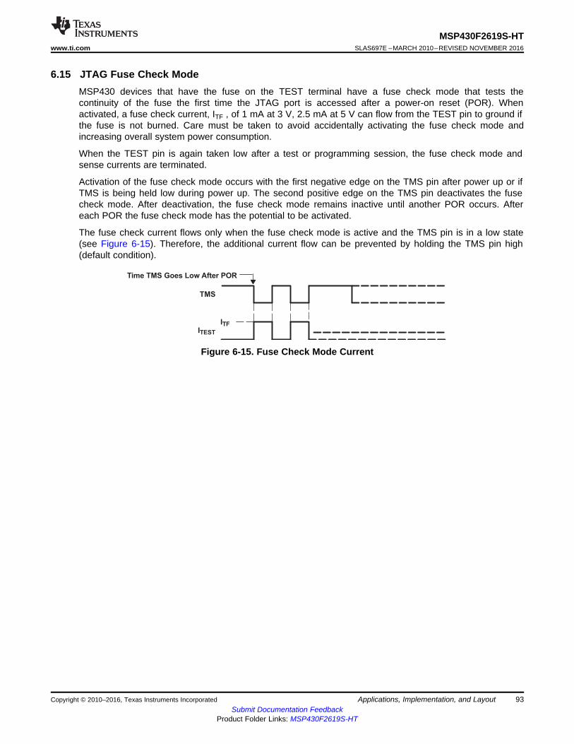
Time TMS Goes Low After POR
TMS
ITF
ITEST
93
MSP430F2619S-HTwww.ti.com SLAS697E –MARCH 2010–REVISED NOVEMBER 2016
Submit Documentation FeedbackProduct Folder Links: MSP430F2619S-HT
Applications, Implementation, and LayoutCopyright © 2010–2016, Texas Instruments Incorporated
6.15 JTAG Fuse Check ModeMSP430 devices that have the fuse on the TEST terminal have a fuse check mode that tests thecontinuity of the fuse the first time the JTAG port is accessed after a power-on reset (POR). Whenactivated, a fuse check current, ITF , of 1 mA at 3 V, 2.5 mA at 5 V can flow from the TEST pin to ground ifthe fuse is not burned. Care must be taken to avoid accidentally activating the fuse check mode andincreasing overall system power consumption.
When the TEST pin is again taken low after a test or programming session, the fuse check mode andsense currents are terminated.
Activation of the fuse check mode occurs with the first negative edge on the TMS pin after power up or ifTMS is being held low during power up. The second positive edge on the TMS pin deactivates the fusecheck mode. After deactivation, the fuse check mode remains inactive until another POR occurs. Aftereach POR the fuse check mode has the potential to be activated.
The fuse check current flows only when the fuse check mode is active and the TMS pin is in a low state(see Figure 6-15). Therefore, the additional current flow can be prevented by holding the TMS pin high(default condition).
Figure 6-15. Fuse Check Mode Current
94
MSP430F2619S-HTSLAS697E –MARCH 2010–REVISED NOVEMBER 2016 www.ti.com
Submit Documentation FeedbackProduct Folder Links: MSP430F2619S-HT
Device and Documentation Support Copyright © 2010–2016, Texas Instruments Incorporated
7 Device and Documentation Support
7.1 Development Tool SupportAll MSP430 microcontrollers include an embedded emulation module (EEM) allowing advanced debuggingand programming through easy-to-use development tools. Recommended hardware options include:• Debugging and programming interface
– MSP-FET430UIF (USB)– MSP-FET430PIF (parallel port)
• Debugging and programming interface with target board– MSP-FET430U64– MSP-FET430U80
• Standalone target board– MSP-TS430PM64
• Production programmer– MSP-GANG430
7.2 Receiving Notification of Documentation UpdatesTo receive notification of documentation updates—including silicon errata—go to the product folder foryour device on ti.com (MSP430F2619S-HT). In the upper right-hand corner, click the "Alert me" button.This registers you to receive a weekly digest of product information that has changed (if any). For changedetails, check the revision history of any revised document.
7.3 Community ResourcesThe following links connect to TI community resources. Linked contents are provided "AS IS" by therespective contributors. They do not constitute TI specifications and do not necessarily reflect TI's views;see TI's Terms of Use.TI E2E™ Online Community The TI engineer-ro-engineer (E2E) community was created to foster
collaboration among engineers. At e2e.ti.com, you can ask questions, share knowledge,explore ideas and help solve problems with fellow engineers.
TI Embedded Processors Wiki Established to help developers get started with Embedded Processorsfrom Texas Instruments and to foster innovation and growth of general knowledge about thehardware and software surrounding these devices.
7.4 TrademarksE2E is a trademark of Texas Instruments.All other trademarks are the property of their respective owners.
7.5 Electrostatic Discharge CautionThis integrated circuit can be damaged by ESD. Texas Instruments recommends that all integrated circuits be handled withappropriate precautions. Failure to observe proper handling and installation procedures can cause damage.
ESD damage can range from subtle performance degradation to complete device failure. Precision integrated circuits may be moresusceptible to damage because very small parametric changes could cause the device not to meet its published specifications.
7.6 GlossaryTI Glossary This glossary lists and explains terms, acronyms, and definitions.
95
MSP430F2619S-HTwww.ti.com SLAS697E –MARCH 2010–REVISED NOVEMBER 2016
Submit Documentation FeedbackProduct Folder Links: MSP430F2619S-HT
Mechanical, Packaging, and Orderable InformationCopyright © 2010–2016, Texas Instruments Incorporated
8 Mechanical, Packaging, and Orderable Information
8.1 Packaging InformationThe following pages include mechanical packaging and orderable information. This information is the mostcurrent data available for the designated devices. This data is subject to change without notice andrevision of this document. For browser-based versions of this data sheet, refer to the left-hand navigation.
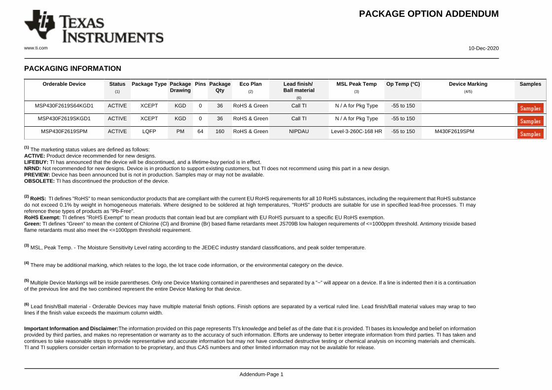
PACKAGE OPTION ADDENDUM
www.ti.com 10-Dec-2020
Addendum-Page 1
PACKAGING INFORMATION
Orderable Device Status(1)
Package Type PackageDrawing
Pins PackageQty
Eco Plan(2)
Lead finish/Ball material
(6)
MSL Peak Temp(3)
Op Temp (°C) Device Marking(4/5)
Samples
MSP430F2619S64KGD1 ACTIVE XCEPT KGD 0 36 RoHS & Green Call TI N / A for Pkg Type -55 to 150
MSP430F2619SKGD1 ACTIVE XCEPT KGD 0 36 RoHS & Green Call TI N / A for Pkg Type -55 to 150
MSP430F2619SPM ACTIVE LQFP PM 64 160 RoHS & Green NIPDAU Level-3-260C-168 HR -55 to 150 M430F2619SPM
(1) The marketing status values are defined as follows:ACTIVE: Product device recommended for new designs.LIFEBUY: TI has announced that the device will be discontinued, and a lifetime-buy period is in effect.NRND: Not recommended for new designs. Device is in production to support existing customers, but TI does not recommend using this part in a new design.PREVIEW: Device has been announced but is not in production. Samples may or may not be available.OBSOLETE: TI has discontinued the production of the device.
(2) RoHS: TI defines "RoHS" to mean semiconductor products that are compliant with the current EU RoHS requirements for all 10 RoHS substances, including the requirement that RoHS substancedo not exceed 0.1% by weight in homogeneous materials. Where designed to be soldered at high temperatures, "RoHS" products are suitable for use in specified lead-free processes. TI mayreference these types of products as "Pb-Free".RoHS Exempt: TI defines "RoHS Exempt" to mean products that contain lead but are compliant with EU RoHS pursuant to a specific EU RoHS exemption.Green: TI defines "Green" to mean the content of Chlorine (Cl) and Bromine (Br) based flame retardants meet JS709B low halogen requirements of <=1000ppm threshold. Antimony trioxide basedflame retardants must also meet the <=1000ppm threshold requirement.
(3) MSL, Peak Temp. - The Moisture Sensitivity Level rating according to the JEDEC industry standard classifications, and peak solder temperature.
(4) There may be additional marking, which relates to the logo, the lot trace code information, or the environmental category on the device.
(5) Multiple Device Markings will be inside parentheses. Only one Device Marking contained in parentheses and separated by a "~" will appear on a device. If a line is indented then it is a continuationof the previous line and the two combined represent the entire Device Marking for that device.
(6) Lead finish/Ball material - Orderable Devices may have multiple material finish options. Finish options are separated by a vertical ruled line. Lead finish/Ball material values may wrap to twolines if the finish value exceeds the maximum column width.
Important Information and Disclaimer:The information provided on this page represents TI's knowledge and belief as of the date that it is provided. TI bases its knowledge and belief on informationprovided by third parties, and makes no representation or warranty as to the accuracy of such information. Efforts are underway to better integrate information from third parties. TI has taken andcontinues to take reasonable steps to provide representative and accurate information but may not have conducted destructive testing or chemical analysis on incoming materials and chemicals.TI and TI suppliers consider certain information to be proprietary, and thus CAS numbers and other limited information may not be available for release.
PACKAGE OPTION ADDENDUM
www.ti.com 10-Dec-2020
Addendum-Page 2
In no event shall TI's liability arising out of such information exceed the total purchase price of the TI part(s) at issue in this document sold by TI to Customer on an annual basis.
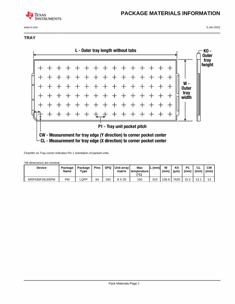
TRAY
Chamfer on Tray corner indicates Pin 1 orientation of packed units.
*All dimensions are nominal
Device PackageName
PackageType
Pins SPQ Unit arraymatrix
Maxtemperature
(°C)
L (mm) W(mm)
K0(µm)
P1(mm)
CL(mm)
CW(mm)
MSP430F2619SPM PM LQFP 64 160 8 X 20 150 315 135.9 7620 15.2 13.1 13
PACKAGE MATERIALS INFORMATION
www.ti.com 5-Jan-2022
Pack Materials-Page 1
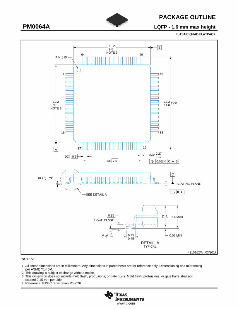
www.ti.com
PACKAGE OUTLINE
C
64X 0.270.1760X 0.5
PIN 1 ID
0.05 MIN
4X 7.5
0.08
TYP12.211.8
(0.13) TYP
1.6 MAX
BNOTE 3
10.29.8
A
NOTE 3
10.29.8
0.750.45
0.25GAGE PLANE
-70
(1.4)
PLASTIC QUAD FLATPACK
LQFP - 1.6 mm max heightPM0064APLASTIC QUAD FLATPACK
4215162/A 03/2017
NOTES: 1. All linear dimensions are in millimeters. Any dimensions in parenthesis are for reference only. Dimensioning and tolerancing per ASME Y14.5M. 2. This drawing is subject to change without notice.3. This dimension does not include mold flash, protrusions, or gate burrs. Mold flash, protrusions, or gate burrs shall not exceed 0.15 mm per side.4. Reference JEDEC registration MS-026.
1
16
17 32
33
48
4964
0.08 C A B
SEE DETAIL A0.08
SEATING PLANE
DETAIL ASCALE: 14DETAIL A
TYPICAL
SCALE 1.400
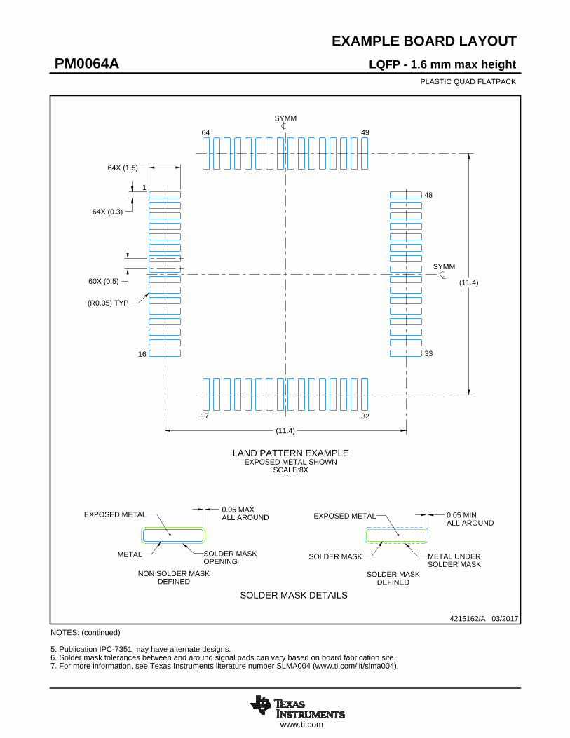
www.ti.com
EXAMPLE BOARD LAYOUT
0.05 MAXALL AROUND 0.05 MIN
ALL AROUND
64X (1.5)
64X (0.3)
(11.4)
(11.4)60X (0.5)
(R0.05) TYP
LQFP - 1.6 mm max heightPM0064APLASTIC QUAD FLATPACK
4215162/A 03/2017
NOTES: (continued) 5. Publication IPC-7351 may have alternate designs. 6. Solder mask tolerances between and around signal pads can vary based on board fabrication site.7. For more information, see Texas Instruments literature number SLMA004 (www.ti.com/lit/slma004).
LAND PATTERN EXAMPLEEXPOSED METAL SHOWN
SCALE:8X
SYMM
SYMM
64 49
17 32
33
481
16
METAL SOLDER MASKOPENING
NON SOLDER MASKDEFINED
SOLDER MASK DETAILS
EXPOSED METAL
SOLDER MASK METAL UNDERSOLDER MASK
SOLDER MASKDEFINED
EXPOSED METAL
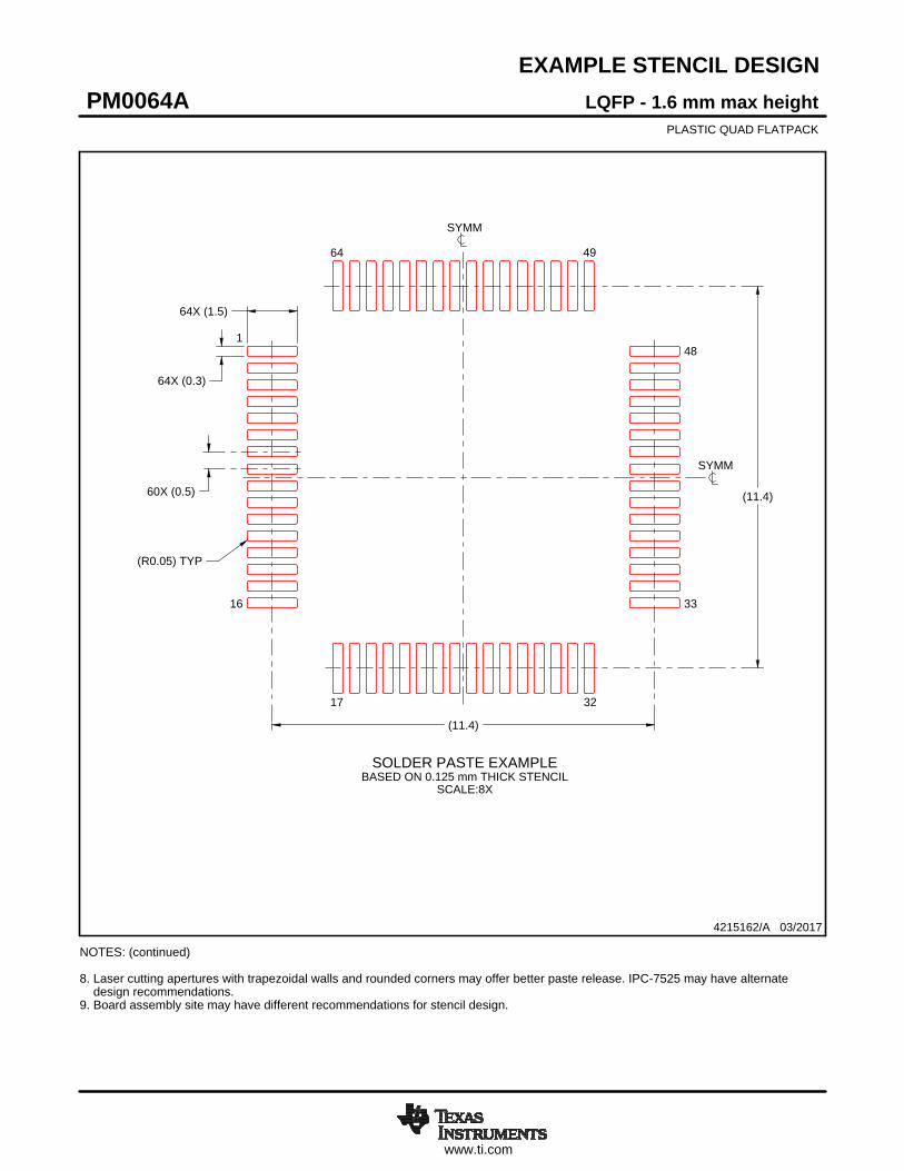
www.ti.com
EXAMPLE STENCIL DESIGN
64X (1.5)
64X (0.3)
60X (0.5)
(R0.05) TYP
(11.4)
(11.4)
LQFP - 1.6 mm max heightPM0064APLASTIC QUAD FLATPACK
4215162/A 03/2017
NOTES: (continued) 8. Laser cutting apertures with trapezoidal walls and rounded corners may offer better paste release. IPC-7525 may have alternate design recommendations. 9. Board assembly site may have different recommendations for stencil design.
SYMM
SYMM
64 49
17 32
33
481
16
SOLDER PASTE EXAMPLEBASED ON 0.125 mm THICK STENCIL
SCALE:8X
IMPORTANT NOTICE AND DISCLAIMERTI PROVIDES TECHNICAL AND RELIABILITY DATA (INCLUDING DATA SHEETS), DESIGN RESOURCES (INCLUDING REFERENCE DESIGNS), APPLICATION OR OTHER DESIGN ADVICE, WEB TOOLS, SAFETY INFORMATION, AND OTHER RESOURCES “AS IS” AND WITH ALL FAULTS, AND DISCLAIMS ALL WARRANTIES, EXPRESS AND IMPLIED, INCLUDING WITHOUT LIMITATION ANY IMPLIED WARRANTIES OF MERCHANTABILITY, FITNESS FOR A PARTICULAR PURPOSE OR NON-INFRINGEMENT OF THIRD PARTY INTELLECTUAL PROPERTY RIGHTS.These resources are intended for skilled developers designing with TI products. You are solely responsible for (1) selecting the appropriate TI products for your application, (2) designing, validating and testing your application, and (3) ensuring your application meets applicable standards, and any other safety, security, regulatory or other requirements.These resources are subject to change without notice. TI grants you permission to use these resources only for development of an application that uses the TI products described in the resource. Other reproduction and display of these resources is prohibited. No license is granted to any other TI intellectual property right or to any third party intellectual property right. TI disclaims responsibility for, and you will fully indemnify TI and its representatives against, any claims, damages, costs, losses, and liabilities arising out of your use of these resources.TI’s products are provided subject to TI’s Terms of Sale or other applicable terms available either on ti.com or provided in conjunction with such TI products. TI’s provision of these resources does not expand or otherwise alter TI’s applicable warranties or warranty disclaimers for TI products.TI objects to and rejects any additional or different terms you may have proposed. IMPORTANT NOTICE
Mailing Address: Texas Instruments, Post Office Box 655303, Dallas, Texas 75265Copyright © 2022, Texas Instruments Incorporated