Embed Size (px)
Citation preview

Version: 1.0 Release date: September 8, 2014
Specifications are subject to change without notice.
MT5931 802.11n platform (2.4GHz) Technical Brief
© 2014 MediaTek Inc.
This document contains information that is proprietary to MediaTek Inc. Unauthorized reproduction of this information in whole or in part is strictly prohibited.

MT5931
802.11n platform (2.4GHz) Technical Brief
Table of Contents
1 System Overview .................................................................................................. 4
1.1 General Descriptions................................................................................................................. 4 1.2 Features ..................................................................................................................................... 4 1.3 Applications ................................................................................................................................ 5 1.4 Block Diagram ............................................................................................................................ 5
2 Product Descriptions ........................................................................................... 6
2.1 Pin Descriptions ........................................................................................................................ 6 2.2 Package Information ................................................................................................................ 11 2.3 Ordering Information .............................................................................................................. 16
3 Electrical Characteristics .................................................................................... 17 3.1 PMU Descriptions .................................................................................................................... 17 3.2 Absolute Maximum Ratings .................................................................................................... 17 3.3 Recommended Operating Range ............................................................................................ 18 3.4 PMU Electrical Characteristics................................................................................................ 18 3.5 XOSC32..................................................................................................................................... 19 3.6 DC Electrical Characteristics for 2.8 Volts Operation........................................................... 20 3.7 DC Electrical Characteristics for 1.8 Volts Operation ............................................................ 21
4 Interface ............................................................................................................ 22 4.1 Host Interface (HIF) ............................................................................................................... 22 4.2 EEPROM Interface................................................................................................................... 31 4.3 EFUSE Function ...................................................................................................................... 33
5 Radio Characteristics ......................................................................................... 34
5.1 Tx/Rx Specifications ............................................................................................................... 34 5.2 Current Consumption .............................................................................................................. 37
© 2014 MediaTek Inc. Page 2 of 38
This document contains information that is proprietary to MediaTek Inc. Unauthorized reproduction or disclosure of this information in whole or in part is strictly prohibited.

MT5931
802.11n platform (2.4GHz) Technical Brief
Lists of Tables and Figures
Table 1. Pin descriptions ............................................................................................................................. 10 Table 2. OSC/XTAL frequency selection .................................................................................................... 10 Table 5. Absolute maximum ratings ........................................................................................................... 18 Table 6. Recommended operating range ................................................................................................... 18 Table 7. PMU characteristics ...................................................................................................................... 19
Figure 1. MT5931 block diagram ..................................................................................................................5 Figure 2. MT5931 TFBGA top marking ...................................................................................................... 11 Figure 3. MT5931 TFBGA POD (a) ............................................................................................................. 12 Figure 4. MT5931 TFBGA POD (b) ............................................................................................................. 13 Figure 5. MT5931 WLCSP marking ............................................................................................................ 14 Figure 6. MT5931 WLCSP POD (a) ............................................................................................................ 14 Figure 7. MT5931 WLCSP POD (b) ............................................................................................................ 15 Figure 8. MT5931 WLCSP POD (c) ............................................................................................................ 15 Figure 9. MT5931 WLCSP POD (d) ............................................................................................................ 16 Figure 10. Block diagram of XOSC32 ......................................................................................................... 19 Figure 11. Signal connections to one 4-bit SDIO card and host interrupt ............................................... 22 Figure 12. Bus signal levels ........................................................................................................................ 23 Figure 13. Bus timing diagram (default) ................................................................................................... 23 Figure 14. High-speed timing diagram ...................................................................................................... 24 Figure 15. T-Mode SPI protocol ................................................................................................................. 25 Figure 16. M-Mode SPI protocol ................................................................................................................ 26 Figure 17. eHPI8 single write access ..........................................................................................................27 Figure 18. eHPI8 single read access ...........................................................................................................27 Figure 19. eHPI8 burst write access (data port) ........................................................................................27 Figure 20. eHPI8 burst read access (data port) ........................................................................................ 28 Figure 21. eHPI16 single write access ........................................................................................................ 28 Figure 22. eHPI16 single read access ........................................................................................................ 28 Figure 23. eHPI16 burst write access (data port) ..................................................................................... 29 Figure 24. eHPI16 burst read access (data port) ...................................................................................... 29 Figure 25. eHPI write cycle timing diagram ............................................................................................. 29 Figure 26. eHPI read cycle timing diagram .............................................................................................. 30 Figure 27. EEPROM configuration ............................................................................................................. 31 Figure 28. EEPROM CRC checksum diagram .......................................................................................... 32 Figure 29. EEPROM interface connection ................................................................................................ 32 Figure 30. EEPROM data timing ............................................................................................................... 32 Figure 31 2.4GHz Receiver Specifications................................................................................................. 34
© 2014 MediaTek Inc. Page 3 of 38
This document contains information that is proprietary to MediaTek Inc. Unauthorized reproduction or disclosure of this information in whole or in part is strictly prohibited.

MT5931
802.11n platform (2.4GHz) Technical Brief
1 System Overview
1.1 General Descriptions MT5931 is a Wi-Fi device which includes
• 802.11 b/g/n
• PA
• LNA
• TR-Switch
MT5931 provides the best and most convenient connectivity functions. MT5931 implements advanced and sophisticated radio coexistence algorithms and hardware mechanisms. The enhanced overall quality for simultaneous voice, data, and audio/video transmission on mobile phone and Tablet PC can be achieved. The small package size with low power consumption reduces the PCB layout area.
1.2 Features
• Embedded RISC core for better system level management
• Coexistence: IEEE 802.15.2 external three-wire coexistence scheme to support additional wireless technologies such as 3G, GPS and WiMAX
• Self calibration.
• Integrated switching regulator enables direct connection to battery.
• Best-in-class current consumption performance
• Intelligent BT/WLAN coexistence scheme that goes beyond PTA signaling (for example, transmit window and duration that take into account of protocol exchange sequence, frequency, etc.)
• TFBGA (5.1x5.3mm2) and WLCSP (2.93x3.17mm2) packages
• 2.4GHz single stream 802.11 b/g/n MAC/BB/RF
• 802.11 d/h/k compliant
• Security: WFA WPA/WPA2 personal, WPS2.0, WAPI (hardware)
• QoS: WFA WMM, WMM PS
• Supports 802.11n optional features: STBC, A-MPDU, Blk-Ack, RIFS, MCS Feedback, 20/40 MHz coexistence (PCO), unscheduled PSMP
• Supports 802.11w protected managed frames
• Supports Wi-Fi Direct
• Interface: SDIO 2.0 (4-bit & 1-bit), SPI(TFBGA only) , EHPI-8/16 (TFBGA only)
• Per packet Tx power control
© 2014 MediaTek Inc. Page 4 of 38
This document contains information that is proprietary to MediaTek Inc. Unauthorized reproduction or disclosure of this information in whole or in part is strictly prohibited.

MT5931
802.11n platform (2.4GHz) Technical Brief
1.3 Applications
• Smart phones
• Tablet PC
• Mobile Internet Device (MID)
• Portable Navigation Device (PND)
• Portable Media Player (PMP)
• Portable gaming devices
1.4 Block Diagram
Figure 1. MT5931 block diagram
© 2014 MediaTek Inc. Page 5 of 38
This document contains information that is proprietary to MediaTek Inc. Unauthorized reproduction or disclosure of this information in whole or in part is strictly prohibited.

MT5931
802.11n platform (2.4GHz) Technical Brief
2 Product Descriptions
2.1 Pin Descriptions
Symbol WLCSP bump
TFBGA ball
Description PU/PD I/O
Power ground pin CGND F6 F4 Ground NA VSS CGND G6 F6 Ground NA VSS PAD_VDDK E5 G4 1.2V core power NA VDD PAD_VDDK G6 1.2V core power NA VDD PAD_VDDK G7 1.2V core power NA VDD DVDDIO3 F3 H1 1.8/2.8V host interface I/O power NA VDD CGND F7 Ground NA VSS CGND K1 Ground NA VSS DVDDIO0 G1 K10 1.8 / 2.8V I/O power NA VDD DVDDIO2 J7 1.8/2.8V host interface or PTA I/O
power NA VDD
DVDDIO1 K7 1.8/2.8V PTA I/O power NA VDD
PMU GND_REF B7 B1 Ground NA OUT_FB C7 C3 Buck feedback NA AVDD16_CLDO C8 C2 CLDO feedback NA CLDO B8 C1 CLDO 1.2V output NA REF A8 A1 Bandgap reference point NA AVDD43_REF A7 A2 4.3V reference point NA AGND43_SMPS B6 B3 Ground NA LXBK A6 A3 Buck feedback NA AVDD43_SMPS B5 A4 Buck power NA PALDO A5 A5 PALDO output NA GND_PALDO C5 C5 Ground NA PALDO_FB C6 E5 PALDO remote sense feedback NA PAD_EN D7 B5 PMU enable from host NA I
RTC X32K_IN D6 D1 RTC 32 kHz clock input NA I AVDDRTC D8 D3 RTC power NA VDD AVSSRTC D4 RTC ground NA VSS X32K_OUT D5 D2 RTC 32K output NA O
© 2014 MediaTek Inc. Page 6 of 38
This document contains information that is proprietary to MediaTek Inc. Unauthorized reproduction or disclosure of this information in whole or in part is strictly prohibited.

MT5931
802.11n platform (2.4GHz) Technical Brief
Symbol WLCSP bump
TFBGA ball
Description PU/PD I/O
RF AVDD33_XO C4 A6 XO power NA VDD PAD_ICAL_EXTR F10 External ICAL input NA I TRX_QN E9 TRX Q signal NA I/O TRX_QP E8 TRX Q signal NA I/O TRX_IN E7 TRX I signal NA I/O TRX_IP E6 TRX I signal NA I/O AVDD16_LF D1 E10 LF power NA VDD AVSS16_WF C2 D6 Ground NA VSS AVSS16_WF D2 D7 Ground NA VSS AVDD16_TRX C1 D10 TRX power NA VDD AVSS16_WF B3 D9 Ground NA VSS TRX_IO_N B1 C10 TRX IO signal NA I/O AVSS33_PA A2 A10 Ground NA VSS AVSS33_PA B2 B9 Ground NA VSS TRX_IO_P A1 B10 TRX IO signal NA I/O AVDD33_TX A3 A9 WLAN power NA VDD AVSS33_PA C9 Ground NA VSS AVSS16_VCO B8 Ground NA VSS AVDD16_SX C3 A8 SX power NA VDD AVSS16_WF C6 Ground NA VSS OSC_IN A4 A7 XTAL/OSC input NA I
Digital FSOURCE F7 E1 eFuse power pin NA VDD WI-FI_INT_B F5 E2 WI-FI_INT_B: Wi-Fi component
interrupt output None/SW O
D15 J6 eHPI_DAT15: eHPI data bus bit 15 None/SW I/O WX_REQ: WiMAX co-existence PTA interface
None/SW I
D14 J5 eHPI_DAT14: eHPI data bus bit 14 None/SW I/O WX_INFO: WiMAX co-existence PTA interface
None/SW I
D13 K6 eHPI_DAT13: eHPI data bus bit 13 None/SW I/O WX_NO_GRANT: WiMAX co-existence PTA interface
None/SW O
© 2014 MediaTek Inc. Page 7 of 38
This document contains information that is proprietary to MediaTek Inc. Unauthorized reproduction or disclosure of this information in whole or in part is strictly prohibited.

MT5931
802.11n platform (2.4GHz) Technical Brief
Symbol WLCSP bump
TFBGA ball
Description PU/PD I/O
D12 H6 eHPI_DAT12: eHPI data bus bit 12 None/SW I/O BT_FREQ: BT co-existence PTA interface
None/SW I
D11 H5 eHPI_DAT11: eHPI data bus bit 11 None/SW I/O BT_ACT: BT co-existence PTA interface
None/SW I
D10 H4 eHPI_DAT10: eHPI data bus bit 10 None/SW I/O WLAN_ACT: BT co-existence PTA interface
None/SW O
D9 J4 eHPI_DAT9: eHPI data bus bit 9 None/SW I/O GPIO0_16: GPIO0_16 in/out None/SW I/O
D8 K4 eHPI_DAT8: eHPI data bus bit 8 None/SW I/O GPIO0_17: GPIO0_17 in/out None/SW I/O
D7 E3 eHPI_DAT7: eHPI data bus bit 7 None/SW I/O EEDO: EEPROM interface None/SW I GPIO0_18: GPIO0_18 in/out None/SW I/O
D6 G3 eHPI_DAT6: eHPI data bus bit 6 None/SW I/O EEDI: EEPROM interface None/SW O GPIO0_19: GPIO0_19 in/out None/SW I/O
D5 G2 eHPI_DAT5: eHPI data bus bit 5 None/SW I/O EECS: EEPROM interface None/SW O GPIO0_20: GPIO0_20 in/out None/SW I/O
D4 G1 eHPI_DAT4: eHPI data bus bit 4 None/SW I/O EESK: EEPROM interface None/SW O GPIO0_21: GPIO0_21 in/out None/SW I/O
D3 E8 K2 eHPI_DAT3: eHPI data bus bit 3 None/SW I/O SDIO_DAT3: SDIO data bus bit 3 PU I/O GPIO0_22: GPIO0_22 in/out None/SW I/O
D2 E7 H2 eHPI_DAT2: eHPI data bus bit 2 None/SW I/O SDIO_DAT2: SDIO data bus bit 2 None/SW I/O GPIO0_23: GPIO0_23 in/out None/SW I/O
D1 E6 J3 eHPI_DAT1: eHPI data bus bit 1 None/SW I/O SDIO_DAT1: SDIO data bus bit 1 None/SW I/O GPIO0_24: GPIO0_24 in/out None/SW I/O
D0 F8 H3 eHPI_DAT0: eHPI data bus bit 1 None/SW I/O SDIO_DAT0: SDIO data bus bit 1 None/SW I/O SPI_DIN: SPI interface DIN None/SW I
© 2014 MediaTek Inc. Page 8 of 38
This document contains information that is proprietary to MediaTek Inc. Unauthorized reproduction or disclosure of this information in whole or in part is strictly prohibited.

MT5931
802.11n platform (2.4GHz) Technical Brief
Symbol WLCSP bump
TFBGA ball
Description PU/PD I/O
A0 G7 J1 eHPI_A0: eHPI interface A0 None/SW I SDIO_CMD: SDIO interface CMD None/SW I/O SPI_DOUT: SPI interface DOUT None/SW O
CS_N F3 eHPI_CSN: eHPI interface CS_N None/SW I GPIO0_27: GPIO0_27 in/out None/SW I/O SPI_CS: SPI interface CS None/SW I
WE_N F2 eHPI_WEN: eHPI interface WE_N None/SW I GPIO0_28: GPIO0_28 in/out None/SW I/O SPI_MODE_SEL: SPI interface MODE_SEL
None/SW I
OE_N G8 J2 eHPI_OEN: eHPI interface OE_N None/SW I SDIO_CLK: SDIO interface SD_CLK
None/SW I
SPI_CLK: SPI interface SPI_CLK None/SW I RF_I_CAL D4 RF_I_CAL: Analog pin NA I
OSC_EN: OSC enable in co-clocking platform
None/SW O
ICAP_TRIG_EXT: External trigger event for internal capture debugging
None/SW I
OSC_EN F9 OSC_EN: OSC enable in co-clocking platform
None/SW O
ICAP_TRIG_EXT: External trigger event for internal capture debugging
None/SW I
GPIO_0 G10 ANTSEL_0: Antenna selection #0 PD/SW O UART_DBG_RX: UART debug RXD
None/SW I
GPIO0_8: GPIO0_8 in/out None/SW I/O GPIO_1 H9 ANTSEL_1: Antenna selection #1 PD/SW O
UART_DBG_TX: UART debug TXD
None/SW O
GPIO0_0: GPIO0_0 in/out None/SW I/O BT_PRI G4 H7 BT_PRI: BT co-existence PTA
interface PD I/O
GPIO0_9: GPIO0_9 in/out PD I/O ANTSEL_0 G2 K8 ATNSEL_0: Antenna selection #0 PD/SW O ANTSEL_1 G3 J8 ATNSEL_1: Antenna selection #1 PU/SW O ANTSEL_2 E1 G9 EESK: EEPROM interface PD/SW O
WLAN_ACT: BT co-existence PTA interface
None/SW O
© 2014 MediaTek Inc. Page 9 of 38
This document contains information that is proprietary to MediaTek Inc. Unauthorized reproduction or disclosure of this information in whole or in part is strictly prohibited.

MT5931
802.11n platform (2.4GHz) Technical Brief
Symbol WLCSP bump
TFBGA ball
Description PU/PD I/O
ANTSEL_3 E2 F8 EEDI: EEPROM interface PD/SW O GPIO0_7: GPIO0_7 in/out None/SW I/O
UART_DBG_TX E3 J10 EECS: EEPROM interface None/SW O UART_DBG_TX: UART debug TXD
None/SW O
UART_DBG_RX F1 H10 EEDO: EEPROM interface PD/SW I UART_DBG_RX: UART debug RXD
None/SW I
EXT_INT_B F2 H8 ICAP_TRIG_EXT: External trigger event for internal capture debugging
None/SW I
WLAN_ACT: BT co-existence PTA interface
None/SW O
EXT_INT_B: External interrupt input from Host
None/SW I
XTEST F4 J9 Test mode enable PD I SYSRST_B E4 K9 External system reset active low PU I
Table 1. Pin descriptions
2.1.1 Strapping Table
XTAL_SEL[0] (ANTSEL_0)
XTAL_SEL[1] (ANTSEL_1)
XTAL_SEL[2] (GPIO_1)
Description
0 0 0 24 MHz 1 0 0 19.2 MHz 0 1 0 26 MHz (default) 1 1 0 Reserved 0 0 1 Reserved 1 0 1 52 MHz 0 1 1 Reserved 1 1 1 Reserved
Table 2. OSC/XTAL frequency selection
WLCSP package only supports 26 MHz.
SLOW_SRC (GPIO_0)
Note
1 Internal 0 External
Table 3. Slow clock source selection
© 2014 MediaTek Inc. Page 10 of 38
This document contains information that is proprietary to MediaTek Inc. Unauthorized reproduction or disclosure of this information in whole or in part is strictly prohibited.

MT5931
802.11n platform (2.4GHz) Technical Brief
WLCSP package use SW select Slow clock source.
OSC_SRC 【WI-FI_INT_B】
Note
0 OSC / Co-clocking 1 XTAL
Table 4. Clock source selection
HOST[0] (ANTSEL_2)
HOST[1] (ANTSEL_3)
Note
0 0 eHPI-8 1 0 eHPI-16 0 1 SPI 1 1 SDIO
Table 5. Host interface selection
WLCSP package only supports SDIO.
2.2 Package Information
2.2.1 TFBGA Packaging
Figure 2. MT5931 TFBGA top marking
© 2014 MediaTek Inc. Page 11 of 38
This document contains information that is proprietary to MediaTek Inc. Unauthorized reproduction or disclosure of this information in whole or in part is strictly prohibited.

MT5931
802.11n platform (2.4GHz) Technical Brief
Figure 3. MT5931 TFBGA POD (a)
Dimension in mm.
© 2014 MediaTek Inc. Page 12 of 38
This document contains information that is proprietary to MediaTek Inc. Unauthorized reproduction or disclosure of this information in whole or in part is strictly prohibited.

MT5931
802.11n platform (2.4GHz) Technical Brief
Figure 4. MT5931 TFBGA POD (b)
© 2014 MediaTek Inc. Page 13 of 38
This document contains information that is proprietary to MediaTek Inc. Unauthorized reproduction or disclosure of this information in whole or in part is strictly prohibited.

MT5931
802.11n platform (2.4GHz) Technical Brief
2.2.2 WLCSP Packaging
Figure 5. MT5931 WLCSP marking
Figure 6. MT5931 WLCSP POD (a)
© 2014 MediaTek Inc. Page 14 of 38
This document contains information that is proprietary to MediaTek Inc. Unauthorized reproduction or disclosure of this information in whole or in part is strictly prohibited.

MT5931
802.11n platform (2.4GHz) Technical Brief
Figure 7. MT5931 WLCSP POD (b)
Figure 8. MT5931 WLCSP POD (c)
© 2014 MediaTek Inc. Page 15 of 38
This document contains information that is proprietary to MediaTek Inc. Unauthorized reproduction or disclosure of this information in whole or in part is strictly prohibited.

MT5931
802.11n platform (2.4GHz) Technical Brief
Figure 9. MT5931 WLCSP POD (d)
2.3 Ordering Information
Part number Package MT5931A/B TFBGA MT5931P/B WLCSP
© 2014 MediaTek Inc. Page 16 of 38
This document contains information that is proprietary to MediaTek Inc. Unauthorized reproduction or disclosure of this information in whole or in part is strictly prohibited.

MT5931
802.11n platform (2.4GHz) Technical Brief
3 Electrical Characteristics
3.1 PMU Descriptions MT5931 integrates the Power Management Unit (PMU) which generates power supplies required by the internal circuitry from the battery.
PMU mainly contains Low Dropout Regulators (LDOs), buck converter and control circuits such as Under-Voltage Lockout (UVLO), thermal protection and power-on/off sequencer.
3.1.1 PALDO
PALDO converts the battery input to a 3.3V supply for the use of Wi-Fi RF PA circuits. It is optimized for the given functions by balancing the quiescent current, dropout voltage, line/load regulation, ripple rejection and output noise.
3.1.2 CLDO
One CLDO is integrated in PMU to supply digital core. It converts 1.8V input to 1.2V output which is suited for the digital circuits. The input is typically connected to the buck’s output.
3.1.3 Buck Converter
The regulator is a DC-DC step-down converter (buck converter) which produces programmable power supply from the battery input. Typically it supplies power for the core LDO and RF circuits. The buck converter is optimized for high efficiency, low EMI and low quiescent current.
3.2 Absolute Maximum Ratings
Symbol Parameter Rating Unit DVDDIO0 DVDDIO1 DVDDIO2
1.8V or 2.8V digital power supply -0.3 to 3.6 V
DVDDIO3 (VIO_HOST) 1.8V or 2.8V SDIO digital IO power supply -0.3 to 3.6 V
DVDD Digital 1.2V power supply -0.3 to 3.6 V AVDD_CLDO Internal CLDO power supply -0.3 to 3.6 V AVDD28_*
AVDD33_* RF power supply -0.3 to 3.6 V
AVDD13_* RF power supply -0.3 to 1.8 V
AVDD_SMPS BUCK and PALDO power supply -0.3 to 4.7 V
© 2014 MediaTek Inc. Page 17 of 38
This document contains information that is proprietary to MediaTek Inc. Unauthorized reproduction or disclosure of this information in whole or in part is strictly prohibited.

MT5931
802.11n platform (2.4GHz) Technical Brief
Symbol Parameter Rating Unit AVDD_MISC PMU power supply -0.3 to 4.7 V TSTG Storage temperature -45 to +135 °C
Table 3. Absolute maximum ratings
3.3 Recommended Operating Range
Symbol Parameter Min. Typ,. Max. Unit DVDDIO0 DVDDIO1 DVDDIO2 DVDDIO3
2.8V digital power supply 2.0 2.8 3.6 V
1.8V digital power supply 1.6 1.8 2.0 V
DVDD Digital core power supply 1.08 1.2 1.32 V AVDD13_* RF power supply 1.28 1.35 1.4 V AVDD28_* RF power supply 2.66 2.8 2.94 V AVDD33_* RF power supply 3.14 3.3 3.46 V AVDD_SMPS BUCK and PALDO power supply 2.9 3.8 4.3 V AVDD_MISC PMU power supply 2.3 3.8 4.3 V Tambient Ambient temperature -40 25 85 °C
Table 4. Recommended operating range
3.4 PMU Electrical Characteristics
3.4.1 PMU Characteristics
Parameter Conditions Min. Typ. Max. Unit
PMU_EN = 0: Shut down current VBAT < 2.3V VBAT = 2.3V 15 μA 2.3V < VBAT < 4.3V VBAT = 3.8V 20 μA
PMU_EN = 1: Quiescent current All outputs on VBAT = 4.2V 100 μA PALDO off, CORE LDO and buck converter on VBAT = 4.2V 56 μA
Under Voltage Lock-Out (UVLO) Under voltage rising threshold 2.25 V Under voltage falling threshold 2.15 V
PMU_EN voltage level High voltage 1.4 V Low voltage 1.0 V
© 2014 MediaTek Inc. Page 18 of 38
This document contains information that is proprietary to MediaTek Inc. Unauthorized reproduction or disclosure of this information in whole or in part is strictly prohibited.

MT5931
802.11n platform (2.4GHz) Technical Brief
Parameter Conditions Min. Typ. Max. Unit Thermal shutdown Threshold 150 °C Hysteresis 40 °C LDO enable response time 250 μs SMPS voltage Output voltage (V_BUCK) 1.65 V
Digital core voltage Output voltage (V_D) 1.2 V
WLAN PA voltage Output voltage (V_PALDO) 3.3 V
Table 5. PMU characteristics
3.5 XOSC32
3.5.1 Block Descriptions
The low-power 32-kHz crystal oscillator, XOSC32, is designed to work with an external piezoelectric 32.768 kHz crystal and a load composed of two functional capacitors. See the figure below.
Figure 10. Block diagram of XOSC32
© 2014 MediaTek Inc. Page 19 of 38
This document contains information that is proprietary to MediaTek Inc. Unauthorized reproduction or disclosure of this information in whole or in part is strictly prohibited.

MT5931
802.11n platform (2.4GHz) Technical Brief
3.5.2 Function Specification of XOSC32
Symbol Parameter Min. Typ. Max. Unit AVDDRTC Analog power supply 1 2.8 3 V Tosc Start-up time 1 Sec. Dcyc Duty cycle 30 50 70 % Current consumption 5 μA
Table 8. Function specification of XOSC32
3.5.3 Recommendations for Crystal Parameters for XOSC32
Symbol Parameter Min. Typ. Max. Unit F Frequency range 32,768 Hz GL Drive level 5 uW ∆f/f Frequency tolerance +/- 20 ppm ESR Series resistance 50 KΩ C0 Static capacitance 1.6 pF CL0F
1 Load capacitance 6 12.5 pF
Table 9. Recommended parameters of the 32 kHz crystal
3.6 DC Electrical Characteristics for 2.8 Volts Operation
Symbol Parameter Conditions Min. Max. Unit VIL Input low voltage LVTTL -0.28 0.6 V VIH Input high voltage 2.0 3.08 V
VT- Schmitt trigger negative going threshold voltage
LVTTL 0.68 1.36 V
VT+ Schmitt trigger positive going threshold voltage 1.36 1.7 V
VOL Output low voltage |IOL|=1.6~14 mA -0.28 0.4 V
VOH Output high voltage |IOH|=1.6~14 mA 2.4 VDD28 + 0.28 V
RPU Input pull-up resistance PU=high, PD=low 40 190 KΩ RPD Input pull-down resistance PU=low, PD=high 40 190 KΩ
Table 10. 2.8V DC descriptions
1 CL is the parallel combination of C1 and C2 in the block diagram.
© 2014 MediaTek Inc. Page 20 of 38
This document contains information that is proprietary to MediaTek Inc. Unauthorized reproduction or disclosure of this information in whole or in part is strictly prohibited.

MT5931
802.11n platform (2.4GHz) Technical Brief
3.7 DC Electrical Characteristics for 1.8 Volts Operation
Symbol Parameter Conditions Min. Max. Unit VIL Input lower voltage
LVTTL -0.18 0.4 V
VIH Input high voltage 1.5 1.98 V
VT- Schmitt trigger negative going threshold voltage
LVTTL 0.44 0.88 V
VT+ Schmitt trigger positive going threshold voltage 0.88 1.1 V
VOL Output low voltage |IOL|=1.6~14 mA -0.18 0.4 V
VOH Output high voltage |IOH|=1.6~14 mA 1.4 VDD18 + 0.18 V
RPU Input pull-up resistance PU=high, PD=low 40 190 KΩ RPD Input pull-down resistance PU=low, PD=high 40 190 KΩ
Table 11. 1.8V DC description
© 2014 MediaTek Inc. Page 21 of 38
This document contains information that is proprietary to MediaTek Inc. Unauthorized reproduction or disclosure of this information in whole or in part is strictly prohibited.
MT5931
802.11n platform (2.4GHz) Technical Brief
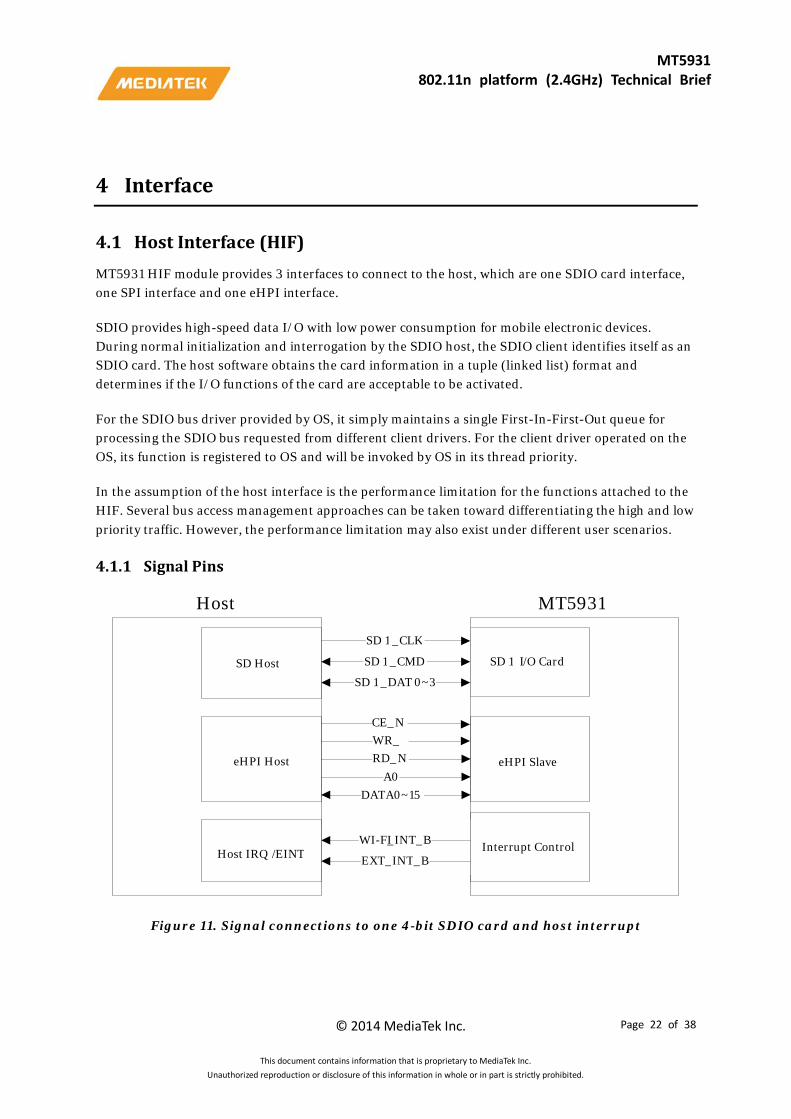
4 Interface
4.1 Host Interface (HIF) MT5931 HIF module provides 3 interfaces to connect to the host, which are one SDIO card interface, one SPI interface and one eHPI interface.
SDIO provides high-speed data I/O with low power consumption for mobile electronic devices. During normal initialization and interrogation by the SDIO host, the SDIO client identifies itself as an SDIO card. The host software obtains the card information in a tuple (linked list) format and determines if the I/O functions of the card are acceptable to be activated.
For the SDIO bus driver provided by OS, it simply maintains a single First-In-First-Out queue for processing the SDIO bus requested from different client drivers. For the client driver operated on the OS, its function is registered to OS and will be invoked by OS in its thread priority.
In the assumption of the host interface is the performance limitation for the functions attached to the HIF. Several bus access management approaches can be taken toward differentiating the high and low priority traffic. However, the performance limitation may also exist under different user scenarios.
4.1.1 Signal Pins
Figure 11. Signal connections to one 4-bit SDIO card and host interrupt
SD Host SD 1 I / O Card
SD 1 _ CLK
SD 1 _ CMD SD 1 _ DAT 0 ~ 3
MT 5931
Interrupt Control
Host
WI-FI _ INT _ B EXT _ INT _ B Host IRQ / EINT
eHPI Slave eHPI Host
CE_N WR_N RD_N
A0 DATA0~15
© 2014 MediaTek Inc. Page 22 of 38
This document contains information that is proprietary to MediaTek Inc. Unauthorized reproduction or disclosure of this information in whole or in part is strictly prohibited.

MT5931
802.11n platform (2.4GHz) Technical Brief
4.1.2 SDIO Timing Waveform
Figure 12. Bus signal levels
Parameter Symbol Min. Max. Unit Conditions
Output high voltage VOH 0.75*VDD V IOH = -100uA VDD min
Output low voltage VOL 0.125*VDD V IOL = 100uA VDD min
Input high voltage VIH 0.625*VDD VDD+0.3 V Input low voltage VIL Vss-0.3 0.25*VDD V
Table 13. Bus signal voltage
Figure 13. Bus timing diagram (default)
V
undefined
Output high level
Output low level
t
VDD
VOH
VIH
VIL
VOL
VSS
VIH
VIL
VIH
VIL
VOH
VOL
Shaded ares are not valid
0.7
0.2
fpp
Input
Output
Clock
tWL tWH
tTLHtTHL
tISU tIH
tODLY(max) tODLY(min)
© 2014 MediaTek Inc. Page 23 of 38
This document contains information that is proprietary to MediaTek Inc. Unauthorized reproduction or disclosure of this information in whole or in part is strictly prohibited.

MT5931
802.11n platform (2.4GHz) Technical Brief
Parameter Symbol Min. Max. Unit Remark Clock CLK (All values are referred to min (VIH) and max (VIL)
Clock frequency data transfer mode fPP 0 25 MHz CCARD ≤ 10 pF (1 card)
Clock frequency identification mode fOD 0/100 400 kHz CCARD ≤ 10 pF (1 card)
Clock low time tWL 10 ns CCARD ≤ 10 pF (1 card) Clock high time tWH 10 ns CCARD ≤ 10 pF (1 card) Clock rise time tTLH 10 ns CCARD ≤ 10 pF (1 card) Clock fall time tTHL 10 ns CCARD ≤ 10 pF (1 card) Inputs CMD, DAT (referenced to CLK)
Input set-up time tISU 5 ns CCARD ≤ 10 pF (1 card) Input hold time tIH 5 ns CCARD ≤ 10 pF (1 card) Outputs CMD, DAT (referenced to CLK)
Output delay time during data transfer mode tOLDY 0 14 ns CL ≤ 10 pF (1 card)
Output delay time during identification mode tOLDY 0 50 ns CL ≤ 10 pF (1 card)
Table 14. Bus timing parameter values (default)
Figure 14. High-speed timing diagram
VIH
VIL
VIH
VIL
VOH
VOL
0.7
0.2
fpp
Input
Output
Clock
tWL tWH
tTLHtTHL
tISU tIH
tODLY(max) tOH
50%VDD
© 2014 MediaTek Inc. Page 24 of 38
This document contains information that is proprietary to MediaTek Inc. Unauthorized reproduction or disclosure of this information in whole or in part is strictly prohibited.

MT5931
802.11n platform (2.4GHz) Technical Brief
Parameter Symbol Min. Max. Unit Remark Clock CLK (All values are referred to min (VIH) and max (VIL)
Clock frequency data transfer mode fPP 0 50 MHz CCARD ≤ 10 pF (1 card) Clock low time tWL 7 ns CCARD ≤ 10 pF (1 card) Clock high time tWH 7 ns CCARD ≤ 10 pF (1 card) Clock rise time tTLH 3 ns CCARD ≤ 10 pF (1 card) Clock fall time tTHL 3 ns CCARD ≤ 10 pF (1 card)
Inputs CMD, DAT (referenced to CLK) Input set-up time tISU 6 ns CCARD ≤ 10 pF (1 card) Input hold time tIH 2 ns CCARD ≤ 10 pF (1 card) Outputs CMD, DAT (referenced to CLK)
Output delay time during data transfer mode tOLDY 14 ns CL ≤ 10 pF (1 card)
Output hold time tOH 2.5 ns CL ≥ 10 pF (1 card) Total system capacitance for each line* CL 40 pF 1 card
*In order to satisfy serve timing, the host shall drive only one card.
Table 15. High-speed timing parameter values
4.1.3 SPI Timing Waveform
MT5931 supports SPI with T-mode and M-mode, 8-/16-/32-bit mode and big/little endian.
Select pin (SPI_MODE_SEL) Mode 0 M-Mode 1 T-Mode
Table 16. SPI mode selection
Figure 15. T-Mode SPI protocol
msb lsb
msb lsb
T - mode
n - 1 n - 3 3 n - 2 2 1 0 spi _ clk
spi _ cs
spi _ din
spi _ dout
© 2014 MediaTek Inc. Page 25 of 38
This document contains information that is proprietary to MediaTek Inc. Unauthorized reproduction or disclosure of this information in whole or in part is strictly prohibited.

MT5931
802.11n platform (2.4GHz) Technical Brief
Figure 16. M-Mode SPI protocol
spi_clk
spi_cs
spi_din
spi_dout
Tclk
Tcss
Tins Tinh
Tod
Tcr Tcf
Symbol Parameter Min. Typ. Max. Unit Tclk SPI clock period 40 ns Tcr/Tcf Clock Rise/Fall time 2.5 ns Tcss CS setup time 7.86 ns Tins Din setup time 5 ns Tinh Din hold time 5 ns Tod Dout output delay 14 ns
Note: This timing spec criterion is VIO = 1.8V. It will gain better performance if stronger VIO is set.
4.1.4 eHPI Timing Waveform
Use the strapping method in section 2.1.1 to set up eHPI-8 or eHPI-16. With eHPI-8 being selected, we need 4 input control pins and 8 data pins, and with eHPI-16 being selected, we need 4 input control pins and 16 data pins. However eHPI-16 can achieve almost twice the data rate for large amount burst data access.
msb lsb
msb lsb
M - mode
n-1 n-3 3n-2 2 1 0spi_clk
spi_cs
spi_din
spi_dout
© 2014 MediaTek Inc. Page 26 of 38
This document contains information that is proprietary to MediaTek Inc. Unauthorized reproduction or disclosure of this information in whole or in part is strictly prohibited.

MT5931
802.11n platform (2.4GHz) Technical Brief
Figure 17. eHPI8 single write access
Figure 18. eHPI8 single read access
Figure 19. eHPI8 burst write access (data port)
© 2014 MediaTek Inc. Page 27 of 38
This document contains information that is proprietary to MediaTek Inc. Unauthorized reproduction or disclosure of this information in whole or in part is strictly prohibited.

MT5931
802.11n platform (2.4GHz) Technical Brief
Figure 20. eHPI8 burst read access (data port)
CE_N
WE_N
RD_N
A0
D[15:0] Di[15:0]A[15:0] Di[31:16]
Figure 21. eHPI16 single write access
CE_N
WE_N
RD_N
A0
D[15:0] Do[15:0]A[15:0] Do[31:16]
Figure 22. eHPI16 single read access
© 2014 MediaTek Inc. Page 28 of 38
This document contains information that is proprietary to MediaTek Inc. Unauthorized reproduction or disclosure of this information in whole or in part is strictly prohibited.
MT5931
802.11n platform (2.4GHz) Technical Brief
CE_N
WE_N
RD_N
A0
D[15:0] A[15:0]
D0[15:0]
D0[31:16]
D1[15:0]
D1[31:16]
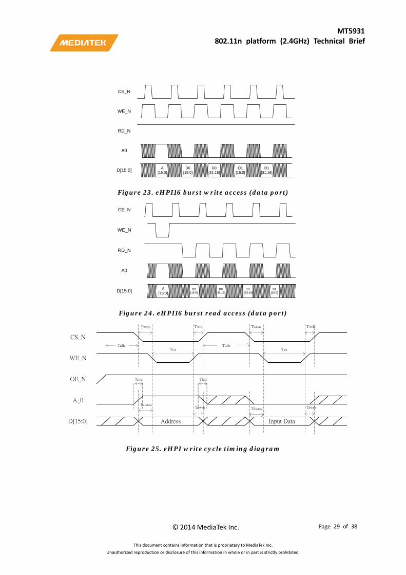
Figure 23. eHPI16 burst write access (data port)
CE_N
WE_N
RD_N
A0
D[15:0] A[15:0]
D0[15:0]
D0[31:16]
D1[23:16]
D1[15:0]
Figure 24. eHPI16 burst read access (data port)
CS_N
WE_N
OE_N
A_0
D[15:0] Address Input Data
Twr
Twrsu Twrh
Twr
Twrsu Twrh
TidleTidle
TdwrsuTdwrh Tdwrsu Tdwrh
Trise Tfall
Figure 25. eHPI write cycle timing diagram
© 2014 MediaTek Inc. Page 29 of 38
This document contains information that is proprietary to MediaTek Inc. Unauthorized reproduction or disclosure of this information in whole or in part is strictly prohibited.

MT5931
802.11n platform (2.4GHz) Technical Brief
Symbol Parameter Min Typ Max Units Twr Write pulse width 40 ns Twrsu CS_N vs WE_N setup time 0 ns Twrh CS_N vs WE_N hold time 0 ns Tdwrsu Data & A_0 vs WE_N setup time 10 ns Tdwrh Data & A_0 vs WE_N hold time 10 ns Tidle Twice Access cycle space Time 40 ns Trise/Tfall Control & Data signals’ Rise/Fall time 5 ns
Table 17. Timing parameter of eHPI write cycle
CS_N
WE_N
OE_N
A_0
D[15:0] Address OutputData
Twr
Twrsu Twrh Trdsu Trdh
Trd
TidleTidle
TdoTdh
Tidle
Tdis
TdwrsuTdwrh
Trise Tfall
Figure 26. eHPI read cycle timing diagram
Symbol Parameter Min Typ Max Units Twr Write pulse width 40 ns Twrsu CS_N vs WE_N setup time 0 ns Twrh CS_N vs WE_N hold time 0 ns Tdwrsu Data & A_0 vs WE_N setup time 10 ns Tdwrh Data & A_0 vs WE_N hold time 10 ns Tidle* Twice access cycle space Time 40 ns Trd Read pulse width 40 ns Trdsu CS_N vs OE_N setup time 0 ns Trdh CS_N vs OE_N hold time 0 ns Tdo Output data delay time 20 ns Tdh Output data hold time 0 ns Tdis Output disable time 20 ns Trise/Tfall Control & data signals’ rise/fall time 5 ns
Table 18. Timing parameter of eHPI read cycle
© 2014 MediaTek Inc. Page 30 of 38
This document contains information that is proprietary to MediaTek Inc. Unauthorized reproduction or disclosure of this information in whole or in part is strictly prohibited.

MT5931
802.11n platform (2.4GHz) Technical Brief
4.2 EEPROM Interface
4.2.1 EEPROM Controller Introduction
MT5931 supports 3-wire serial EEPROM of which the size range is from 128 to 2,048 bytes. The controller operates on the 16-bit data protocol.
4.2.2 EEPROM Content
Word offset Byte offset Content Description Default 0x00 0x00 Signature EEPROM signature. MAC will
automatically load the contents in EEPROM to the corresponding registers if the EEPROM signature is right after being powered on; otherwise, the default values will be used.
0x5931
0x01~0x1B 0x002~0x036 MT5931.CIS0. CISTPL_VERS_1
Content of MT5931 CIS0. Reserved 54 bytes for CISTPL_VERS_1 field.
0x1C 0x38 Checksum Checksum (bit 15 ~ 8) The check sum of data is from word offset 0x01 to word offset 0x1C. The sum from byte 0x2 to byte 0x38 should be 0xFF.
Table 19. EEPROM content
Figure 27. EEPROM configuration
Signature (16’h5931)
5931 CIS 0 CISTPL _ VERS _ 1
Checksum
EEPROM ADR ( Word )
0x00
0x01~0x1B
0x1C
© 2014 MediaTek Inc. Page 31 of 38
This document contains information that is proprietary to MediaTek Inc. Unauthorized reproduction or disclosure of this information in whole or in part is strictly prohibited.

MT5931
802.11n platform (2.4GHz) Technical Brief
4.2.3 EEPROM Checksum Function
Figure 28. EEPROM CRC checksum diagram
After passing the signature of EEPROM controller check, the data will be read from EEPROM. The checksum function will continue until the address reaches 0x1C.
4.2.4 EEPROM Interface Connection
Figure 29. EEPROM interface connection
4.2.5 EEPROM Interface Timing
Figure 30. EEPROM data timing
CheckSumDO[7:0]
DO[15:8]
0xFF
Checksum_error
MT6620EEPROMController
3-WireSerial
EEPROM
EECS
EEDI
EESK
EEDO
EESK
EECS
EEDI
CLK_DC
T = tSK
tDIS tDIH
tPD1tPD0
EECS
EECS
EEDO
EEDI
EESK
© 2014 MediaTek Inc. Page 32 of 38
This document contains information that is proprietary to MediaTek Inc. Unauthorized reproduction or disclosure of this information in whole or in part is strictly prohibited.

MT5931
802.11n platform (2.4GHz) Technical Brief
Description Symbol Min. Max. Unit Notes I2C serial clock tSK 2500 ns 1 Data input setup time tDIS 0.5T - 20 0.5T + 20 ns Data input hold time tDIH 0.5T - 20 0.5T + 20 ns Data output delay to “0” tPD0 500 ns 2 Data output delay to “1” tPD1 500 ns 2
Table 20. EEPROM AC characteristics
Note:
1 It supports I2C fast mode up to 400 kHz.
2 The data output direction is from EEPROM slave to MT5931 master. This parameter depends on the EEPROM device.
4.3 EFUSE Function There are some EFUSE macros inside MT5931. EFUSE macro is a one-time-programming (OTP) non-volatile memory used to store sensitive and important data. The EFUSE controller delivers EFUSE status and re-initializes EFUSE macro. Users can program EFUSE via the EFUSE controller by proper configuration and sequences.
© 2014 MediaTek Inc. Page 33 of 38
This document contains information that is proprietary to MediaTek Inc. Unauthorized reproduction or disclosure of this information in whole or in part is strictly prohibited.

MT5931
802.11n platform (2.4GHz) Technical Brief
5 Radio Characteristics
5.1 Tx/Rx Specifications
5.1.1 2.4GHz Receiver Specifications
Figure 31 2.4GHz Receiver Specifications
Note: All specifications are measured at the antenna port unless otherwise specified.
Parameter Description Min. Typ. Max. Unit Frequency range 2412 - 2,484 MHz
Rx sensitivity*
1 Mbps DSSS -96 dBm 2 Mbps DSSS -94 dBm 5.5 Mbps DSSS -91 dBm 11 Mbps DSSS -88.5 dBm
Rx sensitivity*
6 Mbps OFDM -92.5 dBm 9 Mbps OFDM -90.5 dBm 12 Mbps OFDM -89.5 dBm 18 Mbps OFDM -87 dBm 24 Mbps OFDM -84 dBm 36 Mbps OFDM -80 dBm 48 Mbps OFDM -76.5 dBm 54 Mbps OFDM -75 dBm
RX sensitivity* BW = 20 MHz Green field 800ns guard interval Non-STBC
MCS 0 -92 dBm MCS 1 -88.5 dBm MCS 2 -86.5 dBm MCS 3 -83.5 dBm MCS 4 -80.5 dBm MCS 5 -76 dBm MCS 6 -74.5 dBm MCS 7 -73 dBm
Rx sensitivity* MCS 0 -89 dBm
© 2014 MediaTek Inc. Page 34 of 38
This document contains information that is proprietary to MediaTek Inc. Unauthorized reproduction or disclosure of this information in whole or in part is strictly prohibited.

MT5931
802.11n platform (2.4GHz) Technical Brief
Parameter Description Min. Typ. Max. Unit BW = 40 MHz Green field 800ns guard interval Non-STBC
MCS 1 -85.5 dBm MCS 2 -83.5 dBm MCS 3 -80.5 dBm MCS 4 -77.5 dBm MCS 5 -73 dBm MCS 6 -71.5 dBm MCS 7 -69.5 dBm
Maximum receive level
11 Mbps DSSS -3 dBm 6 Mbps OFDM -3 dBm 54 Mbps OFDM -3 dBm MCS0 -3 dBm MCS7 -3 dBm
Adjacent channel rejection (30 MHz offset)
1 Mbps DSSS 40 dB
Adjacent channel rejection (25 MHz offset)
11 Mbps DSSS 40 dB
Adjacent channel rejection (25 MHz offset)
6 Mbps OFDM 37 dB
54 Mbps OFDM 25 dB
Adjacent channel rejection (25 MHz offset), BW = 20 MHz
MCS 0 33 dB
MCS 7 18 dB
Adjacent channel rejection (40 MHz offset), BW = 40 MHz
MCS 0 33 dB
MCS 7 18 dB
Blocking level at RF port (with external filter)
848.8 MHz GSM 28 dBm 914.8 MHz GSM 28 dBm 1784.8 MHz GSM 5 dBm 1909.8 MHz GSM 5 dBm 1907.6 MHz WCDMA 17 dBm 1977.6 MHz WCDMA 17 dBm
* Rx sensitivity degradation 1.5dB drops by WLCSP package type.
Table 21. 2.4GHz receiver specification
© 2014 MediaTek Inc. Page 35 of 38
This document contains information that is proprietary to MediaTek Inc. Unauthorized reproduction or disclosure of this information in whole or in part is strictly prohibited.

MT5931
802.11n platform (2.4GHz) Technical Brief
5.1.2 2.4GHz Transmitter Specifications
Parameter Description Min. Typ. Max. Unit Frequency range 2412 - 2,484 MHz
Output power
802.11b, 1~11 Mbps DSSS 18.5 dBm 802.11g, 6 ~ 54Mbps OFDM 15.5 dBm 802.11n, HT20 MCS0 ~ 7 15.5 dBm 802.11n, HT40 MCS0 ~ 7 13.5 dBm
Tx power accuracy ±1.5 dB
Carrier suppression 30 dBc
Return loss 8 dB
Transmitted power
76 ~ 108 MHz -143 dBm/Hz 776 ~ 794 MHz -143 dBm/Hz 869 ~ 960 MHz -143 dBm/Hz 925 ~ 960 MHz -143 dBm/Hz 1570 ~ 1,580 MHz -143 dBm/Hz 1,805 ~ 1,880 MHz -143 dBm/Hz 1,930 ~ 1,990 MHz -143 dBm/Hz 2,110 ~ 2,170 MHz -143 dBm/Hz
Harmonic output power
2nd harmonic -44 dBm/MHz
3rd harmonic -58 dBm/MHz
Table 22. 2.4GHz transmitter specification
© 2014 MediaTek Inc. Page 36 of 38
This document contains information that is proprietary to MediaTek Inc. Unauthorized reproduction or disclosure of this information in whole or in part is strictly prohibited.
MT5931
802.11n platform (2.4GHz) Technical Brief
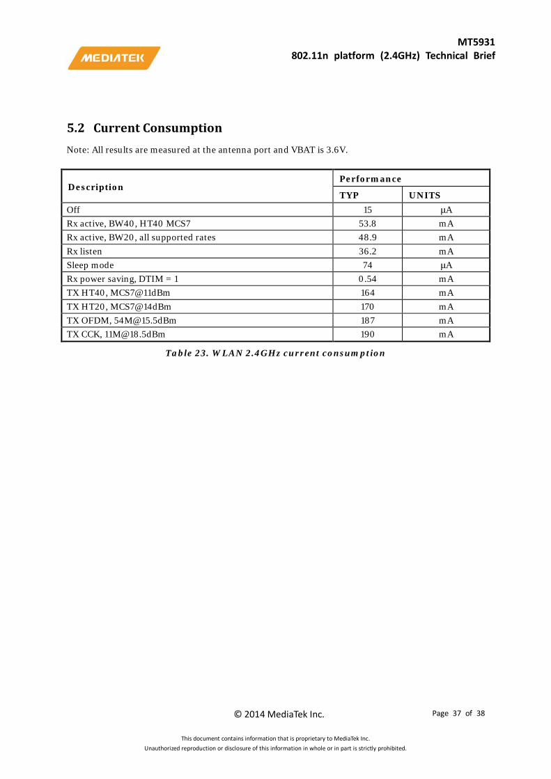
5.2 Current Consumption Note: All results are measured at the antenna port and VBAT is 3.6V.
Description Performance
TYP UNITS Off 15 μA Rx active, BW40, HT40 MCS7 53.8 mA Rx active, BW20, all supported rates 48.9 mA Rx listen 36.2 mA Sleep mode 74 μA Rx power saving, DTIM = 1 0.54 mA TX HT40, MCS7@11dBm 164 mA TX HT20, MCS7@14dBm 170 mA TX OFDM, [email protected] 187 mA TX CCK, [email protected] 190 mA
Table 23. WLAN 2.4GHz current consumption
© 2014 MediaTek Inc. Page 37 of 38
This document contains information that is proprietary to MediaTek Inc. Unauthorized reproduction or disclosure of this information in whole or in part is strictly prohibited.
MT5931
802.11n platform (2.4GHz) Technical Brief
ESD CAUTION
MT5931 is ESD (electrostatic discharge) sensitive device and may be damaged with ESD or spike voltage. Although MT5931 is with built-in ESD protection circuitry, please handle with care to avoid the permanent malfunction or the performance degradation.
© 2014 MediaTek Inc. Page 38 of 38
This document contains information that is proprietary to MediaTek Inc. Unauthorized reproduction or disclosure of this information in whole or in part is strictly prohibited.