Embed Size (px)
Citation preview
Chapter 7
Multi-Hole Waveguide Directional Couplers
Mahmoud Moghavvemi,Hossein Ameri Mahabadi and Farhang Alijani
Additional information is available at the end of the chapter
http://dx.doi.org/10.5772/51355
1. Introduction
The directional couplers are inherently assumed as four-port devices, which consisted oftwo transmission lines that are electromagnetically coupled to each other. The first port isnamed as input, and the second one as output or transmitted, the third one as sampling orcoupled and the fourth one as isolated or terminated. By using a special design the inputpower is divided between output and coupled port in a certain ratio named coupling factor.The required value for coupling factor P1/P3 defines the range of applications for directionalcouplers. Based on the application, coupling factor could be any value like 3, 6, 10, 20 dBand even more. The performance of the directional coupler is usually evaluated by its direc‐tivity between port 3 and 4.The directivity is a calculated parameter from isolation and cou‐pling factor and shows how the two components of wave cancel each other at port 4.Though we prefer to have high value for directivity as much as possible, but in real situationthis could be happened only around center frequency of designing band. The waveguide di‐rectional couplers have a good directivity compared to microstrip or stripline couplers andin spite of their bulky size, give us a low loss, high power handling, good characteristics andlow cost due to use of just a simple waveguide.
Nowadays the numerical methods are widely used for simulation and optimization of highfrequency structures. Some of them such as HFSS and FEKO, are well commercialized andused widely by researchers and engineers.. But for designing procedure and for startingpoint we need an initialization value to input into simulator and then optimize the parame‐ters by its internal routines.
In this chapter we focus on the waveguide directional couplers and we try to give a goodreference as well as finalized designing formulas in closed form and tables to be used indi‐vidually or as initial values for numerical software. The full generalized field theory and its
© 2012 Moghavvemi et al.; licensee InTech. This is an open access article distributed under the terms of theCreative Commons Attribution License (http://creativecommons.org/licenses/by/3.0), which permitsunrestricted use, distribution, and reproduction in any medium, provided the original work is properly cited.
equations for designing based on multi-hole coupling structure will be introduced, thoughmore detailed basic information could be found in given references.
Moreover, by solving the equations, the recursive procedure is employed in a computer pro‐gram to adjust the required directivity, coupling and frequency or waveguide type to speci‐fy the number of coupling holes, individual diameters and locations of holes in waveguide’scoordinate. Besides of those parameters, the length of coupler, matched load and other sizesof structure for fabricating, will be defined too. By using the different methods like bino‐mial, Chebyshev, and super imposed to calculate the coupling of each hole, the wide band‐width response is achieved. At the end, a number of books and papers are given as goodreferences for further study.
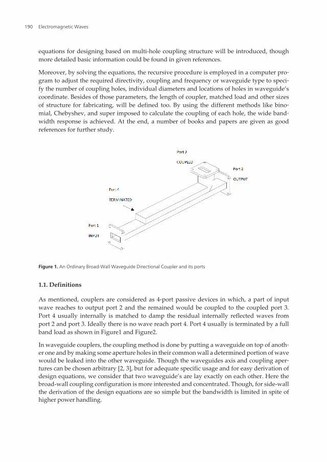
Figure 1. An Ordinary Broad-Wall Waveguide Directional Coupler and its ports
1.1. Definitions
As mentioned, couplers are considered as 4-port passive devices in which, a part of inputwave reaches to output port 2 and the remained would be coupled to the coupled port 3.Port 4 usually internally is matched to damp the residual internally reflected waves fromport 2 and port 3. Ideally there is no wave reach port 4. Port 4 usually is terminated by a fullband load as shown in Figure1 and Figure2.
In waveguide couplers, the coupling method is done by putting a waveguide on top of anoth‐er one and by making some aperture holes in their common wall a determined portion of wavewould be leaked into the other waveguide. Though the waveguides axis and coupling aper‐tures can be chosen arbitrary [2, 3], but for adequate specific usage and for easy derivation ofdesign equations, we consider that two waveguide’s are lay exactly on each other. Here thebroad-wall coupling configuration is more interested and concentrated. Though, for side-wallthe derivation of the design equations are so simple but the bandwidth is limited in spite ofhigher power handling.
Electromagnetic Waves190
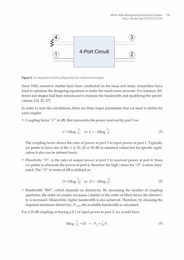
Figure 2. An equivalent 4-Port configuration for a directional coupler
Since 1945, extensive studies have been conducted on the issue and many researchers havetried to optimize the designing equations to make the result more accurate. For instance, dif‐ferent slot shapes had been introduced to increase the bandwidth and modifying the specifi‐cations. [12, 25, 27]
In order to start the calculations, there are three major parameters that we need to define foreach coupler:
• Coupling factor “C” in dB, that represents the power received by port 3 as:
C =10logPi
P f or C = - 10log
P f
Pi(1)
The coupling factor shows the ratio of power at port 3 to input power at port 1. Typicallywe prefer to have one of the 3, 6, 10, 20 or 30 dB as standard values but for specific appli‐cation it also can be defined freely.
• Directivity “D”, is the ratio of output power at port 3 to received power at port 4. Sincewe prefer to eliminate the power at port 4, therefore the high values for “D” is more inter‐ested. The ”D” in terms of dB is defined as:
D =10logP f
Pb or D = - 10log
Pb
P f(2)
• Bandwidth “BW”, which depends on directivity. By increasing the number of couplingapertures, the order of coupler increases ( similar to the order of filter) hence the directivi‐ty is increased. Meanwhile, higher bandwidth is also achieved. Therefore, by choosing therequired minimum directivity, D min, the available bandwidth is calculated.
For a 10 dB coupling or having a 0.1 of input power to port 3, we would have:
10logP f
Pb=10 → P f = 1
10 Pi (3)
Multi-Hole Waveguide Directional Couplershttp://dx.doi.org/10.5772/51355
191
In the same way, for a 3dB coupling, half of input power will receive to port 3:
10logPi
P f=3 → P f = 1
2 Pi (4)
And if we consider D = 40 dB for directivity:
10logP f
Pb=40 → P f =10000Pb (5)
It is the adequate value for designing a good directional coupler.
A number of references, which have studied the couplers and have given the relationshipbetween number of aperture holes “n” and directivity “D” are listed in references [12, 25,23]. In addition to number of aperture holes”n”, in the designing procedure for directionalcouplers, certain parameters should be well defined as:
• Distances between the holes
• Distances between holes to side-wall (holes center offset from waveguide axis)
• The holes dimensions (diameter of holes for circular holes).
It has been shown that to have an optimum coupling around a certain frequency, the criteria(6) should be kept in which “x” is the distance between the holes centers to the side-wall and“a” is the broad wall size of waveguide: [24]
xa ≤0.25 (6)
Furthermore, by precise study, the best design value for ratio of (6) is given as [23]
xa =0.203 (7)
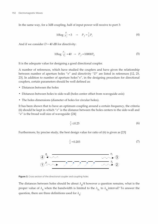
Figure 3. Cross section of the directional coupler and coupling holes
The distances between holes should be about λg/4 however a question remains, what is theproper value of λg when the bandwidth is limited to the λg1
to λg2interval? To answer the
question, there are three definitions used for λg:
Electromagnetic Waves192
1. λg is the average of wavelength of lower band λg1 and upper band λg2 so:
λg =λg 1 + λg 2
2 →λg
4 = 18 (λg 1 + λg 2) (8)
2. λg can be considered as geometric mean between λg 1 and λg 2 :
λg = λg 1.λg 2 → λg
4 = 14 λg 1.λg 2
(9)
3. λg can be considered as mean value between λg 1 and λg 2:
2λg
= 1λg 1
+ 1λg 2
→λg =2λg 1λg 2
λg 1 + λg 2 →
λg
4 =λg 1λg 2
2(λg 1 + λg 2) (10)
The best choice for defining the centers of two holes is the 3rd definition since it has beenpractically approved too [23]. So the wavelength would be derived from (10). Therefore, inorder to define the dimensions of each hole (or diameter in case of circular hole type), theeach hole’s coupling should be calculated first, and the hole’s diameter would be derivedconsequently.
1.2. Fields Equations
In order to calculate the coupling of each hole and by using the required Dmin that we need‐here, the number of holes “n” will be derived in two different ways:
i- The coupling coefficient mapped to coefficients of nth order of Chebyshev polynomial.
ii- The coupling coefficient mapped to coefficients of nth order of Binomial polynomial.
By assuming the same order for polynomials “i” and “ii” and by noticing that the directivityslope in case of “i” is higher, we expect to have higher bandwidth in comparizon to “ii” andlimited ripple in pass-band. In case of “ii” though there is no ripple in pass-band but theslope of directivity is lower than “i” with same order of polynomial, therefore the band‐width is lower than “i”. For years many of manufacturers chose the “i” method and consid‐ering the number of holes n = 20. Here, the “i” method is chosen, however the number ofholes “n” would be defined from Dmin and it will be not fixed anymore.
In fabricating the couplers, any arbitrary shape for holes can be used but the circular; ellipticand rounded-edge rectangle has been widely studied, simulated and used in research reports.[30] Here, the circular holes have been adopted. The circular holes can be aligned in one, two orthree parallel rows, but in our case, 2-rows are used. In order to calculate the coupling coeffi‐cients and related field equations the “Bethe’s small-hole coupling theory” is used as the maincomputational method. Further, by using a correcting function, the theory is expanded to usebig-size holes as well [12, 26, 27]. In that way, Levi’s work would be followed to find the effectof wall-thickness “t” and also the relationship between variations of directivity “D” and cou‐pling error “ΔC”. [27]. Levi showed that if “D” increases, “ΔC” will decrease.
Multi-Hole Waveguide Directional Couplershttp://dx.doi.org/10.5772/51355
193
In special case, if we require high directivity “D”, like “D = 50 dB” for small bandwidth like8.9 to 9 GHz, only 2 holes are needed to synthesis the coupler.
For calculating the distance of holes’ centers to side-wall “x”, the equation sin πxa =
λ0
6a is used
in which “a” is broad-side of waveguide and λ0 is the wavelength in the middle of the band. [2]
The coupled wave equations for incident wave A1 and reflected B1by assuming the sameamplitude for waves are as follows:
A1 = j 2πabλg
M xH x(1)H x
(2) + M zH z(1)H z
(2) - PEy(1)Ey
(2) (11)
B1 = j 2πabλg
-M xH x(1)H x
(2) + M zH z(1)H z
(2) - PEy(1)Ey
(2) (12)
In which, “a” and “b” are the waveguide dimensions, M x and M z are the magnetic polariza‐
tion components in “x” and “z” axis and P is electrical polarization. The H x(1) is the ampli‐
tude’s wave component in the first waveguide and H x(2)is for second and so on. If two
waveguides are identical then H x(1) = H x
(2) and H z(1) = H z
(2). Then the fields’ components are ex‐pressed as:
H x = - Sin πxa e - jγz (13)
H z = jλg
2a Cos πxa e - jγz (14)
Ey =λg
λ Sin πxa e - jγz (15)
The field equations are given separately for “Narrow wall” and “Broad wall” cases. Here,we briefly introduce them and give the relations for our interested one (i.e., Broad wall):
1.2.1. Narrow wall
By referring to Figure 5, since x =0, the equations could be simplified as:
A1 = A2 = -jλg M z
2a 3b(16)
In which, M z is independent from frequency. In other words, “Narrow wall” coupling hassignificant difference comparing to “Broad wall” coupling.
Electromagnetic Waves194
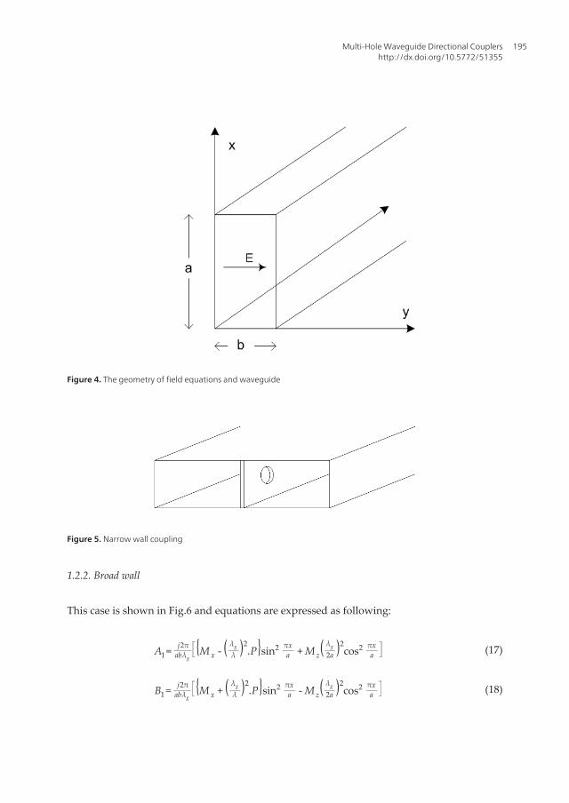
Figure 4. The geometry of field equations and waveguide
Figure 5. Narrow wall coupling
1.2.2. Broad wall
This case is shown in Fig.6 and equations are expressed as following:
A1 = j2πabλg
{M x - ( λg
λ )2.P}sin2 πx
a + M z( λg
2a )2cos2 πx
a (17)
B1 = j2πabλg
{M x + ( λg
λ )2.P}sin2 πx
a - M z( λg
2a )2cos2 πx
a (18)
Multi-Hole Waveguide Directional Couplershttp://dx.doi.org/10.5772/51355
195
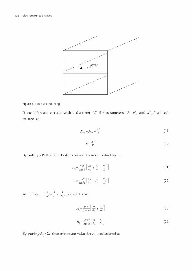
Figure 6. Broad-wall coupling
If the holes are circular with a diameter “d” the parameters “P , M x and M z ” are cal‐
culated as:
M x =M z = d 3
6 (19)
P = d 3
12 (20)
By putting (19 & 20) in (17 &18) we will have simplified form:
A1 = jπd 3
12a 2b2aλg
+λg
2a -aλg
λ 2 (21)
B1 = jπd 3
12a 2b2aλg
-λg
2a +aλg
λ 2 (22)
And if we put 1λ2 = 1
λg2 - 1
(2a)2 we will have:
A1 = jπd 3
24a 2b2aλg
+λg
2a (23)
B1 = jπd 3
24a 2b6aλg
-λg
2a (24)
By putting λg =2a then minimum value for A1 is calculated as:
Electromagnetic Waves196
A10 = jπd 3
12a 2b(25)
And coupling variation to frequency changing is:
ΔC =20log2aλg
+λg2a
2(26)
On the other hand, variation of directivity to frequency is given by:
D=20logA1
B1=20log
2aλg
+λg2a
6aλg
-λg2a
(27)
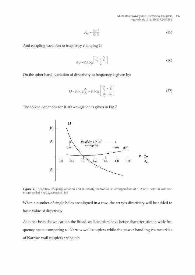
The solved equations for R100 waveguide is given in Fig.7
Figure 7. Theoretical coupling variation and directivity for transverse arrangements of 1, 2 or 3 holes in commonbroad-wall of R100 waveguide.[14]
When a number of single holes are aligned in a row, the array’s directivity will be added to
basic value of directivity.
As it has been shown earlier, the Broad-wall couplers have better characteristics in wide fre‐
quency spans comparing to Narrow-wall couplers while the power handling characteristic
of Narrow-wall couplers are better.
Multi-Hole Waveguide Directional Couplershttp://dx.doi.org/10.5772/51355
197
1.3. Coupling by big holes
The equations given in section 1.3 were valid for small holes. By considering the wall-thick‐ness “t” and big hole’s by surface size of “A”, the equations should be corrected. This hasalready done and the results will be used now. [15]
1.3.1. Corrections for wall thickness “t”
When the coupling holes have thickness “t”, it equals to a short-length circular waveguide,which is working under its cut-off frequency (when frequency is lower than resonance fre‐quency). Therefore the amplitude of the coupled wave attenuates by following term:
exp{ -2πtAλc
1 - ( λc
λ )21
2} (28)
In which, the λc is the cut-off wavelength of hole and λ is the wavelength in operating fre‐quency, “t ” is the wall-thickness and “A” is the correction factor which includes the interac‐tions of adjacent fields and is defined practically. [15] For elliptic holes (Narrow slot) the“A” factor is in 3rd order but for circular holes it is close to first order. If the fields have multicomponents, correction factor (28) should be applied on all of the Bethe’s equations. Itmeans that in equations (17) and (18) the magnetic field correction factor for coupling have aparameter λc that is due to excitation by TE 11 mode so for this mode λc →λH =1.705d andcorrection factor for electric field coupling uses a λc, which relates to TM 01 mode and equalsto λc →λE =1.305d .
1.3.2. Corrections for big size holes
A good study for such big size holes have been done by an equivalent circuit. [15] In thisway, the hole’s effect will be simulated by a two port network in parallel or in series be‐tween two waveguides which have mutual coupling. This network is a lossless and shouldbe defined by Foster’s reactance theorem. Here, the impedance will be defined by locationsof its zeroes and poles in addition to the multiplications coefficients.
In simple expression of Bethe’s small sized coupling hole theory, this impedance has a sim‐ple form. For example the reactance of a small hole in a thin diaphragm at the cross sectionof a rectangular waveguide, working in TE10 is:
X =4πM Z0
abλg(29)
In which, the “a” and “b” are the waveguide dimensions that have been shown in Fig.4
Electromagnetic Waves198
The term λg is the guided wavelength, “M” magnetic polarization, Z0 characteristic impe‐
dance of the waveguide. The Z0 has a direct relation to term λg
λ , which shows that lumpedreactance “X” has a direct relation to frequency (X∝ f) too.
Therefore the small hole coupling theory assumes that the “X” would be a constant reac‐tance but it is not true. Because, there are a few numbers of unwanted resonances occurredin the frequency band. For this reason the (29) would be a good definition when the operat‐ing frequency is somehow lower than the first resonance. For considering the resonance ef‐fect in equation (29), the corrected “M” would be expressed by introducing a new term that
considers the effect of cut-off wavelength M
1 - ( f 2
f c2 ) and the result is as follows:
XZ0
= 4πM
abλg(1 - ( f 2
f c2 )) (30)
From measurements, it has been shown that the above correction factor gives a good ap‐proximation.
The attenuation definition (28) can be combined to (30) to give us a general correction factorfor big size holes:
exp{ -2πtAλc
1 - ( f 2
f c2 )
1
2}1 - ( f 2
f c2 )
(31)
1.4. Multi holes coupling
A longitudinal coupling consists of a series of holes by center distance of λg
4 that has a greatcoupling in forward and weak coupling in backward direction.
The slight coupling for a single hole has been studied and the directivity introduced by:
Directivity (dB)=20logA1
B1(32)
In which: [15]
A1
B1=
∫-L /2
L /2ϕ(x )dx
∫-L /2
L /2ϕ(x )exp ( - 2 jβx)dx
(33)
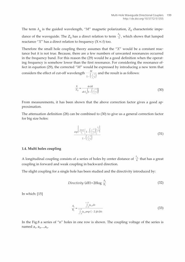
In the Fig.8 a series of “n” holes in one row is shown. The coupling voltage of the series isnamed a1, a2,...,an.
Multi-Hole Waveguide Directional Couplershttp://dx.doi.org/10.5772/51355
199
Figure 8. The cross section of n-Hole array and coupling coefficients
All the hole’s center distances and electrical length are the same and are considered in the
middle of the band. If the input wave to port 1 has constant amplitude and matched to other
3 ports, the reflected wave can be expressed by:
B1 =a1 + a2Exp(-2 jϕ) + a3Exp(-4 jϕ) + … + anExp(-2(n - 1) jϕ) (34)
The interesting and useful case is when the coefficients of the series being symmetrical from
center. Therefore:
a1 =an, a2 =an-1, aK =an-K +1 (35)
So by putting the values (35) into (34):
B1 ={ 2a1cos (n - 1)ϕ + 2a2cos (n - 2)ϕ + … + 2an/2cos ϕ e j(n-1)ϕ n even
2a1cos (n - 1)ϕ + 2a2cos (n - 2)ϕ + … +an+1
2 e j(n-1)ϕ n odd (36)
The direct coupled wave at port 3 will be:
A1 =∑r=1n ar e
j(n-1)ϕ (37)
And the directivity “D” is calculated by normalizing B1 to A1 in (36) by dividing the sum of
each coupling voltages. In special case if there are “n” identical holes, therefore:
B1
A1= sin nϕ
n sin ϕ (38)
Electromagnetic Waves200
2. Design methods based on arrays
2.1. Chebyshev Array
If the minimum voltage over the full bandwidth to reach a good directivity “D” is needed,the Chebyshev polynomial can be used for distribution function of each hole’s voltage. Suchcoefficients are derived by putting the B1 in (36) by considering the following equal ripple’sdirectivity function as following:
B1 =amTn-1( cos ϕcos ϕ0
) (39)
In which the am is the maximum of B1 over the coupling bandwidth that given by following:
ϕ0≤ϕ ≤π - ϕ0 (40)
The am is calculated by putting the ϕ =0 in (39):
am =∑r=1
nar
T n-1( 1cos ϕ0
) =|A1|
T n-1( 1cos ϕ0
) (41)
In (36) if we put ϕ =0:
B1 =∑r=1
nar (42)
Therefore the minimum directivity over the bandwidth would be:
Dmin =20log Tn-1( 1cos ϕ0
) (43)
Comparing this method to method of Binomial polynomial is very informative that has beendone by Levi. In this case we should have: [16]
B1 =am '( cos ϕcos ϕ0
)n-1 (44)
In which:
am ' =∑r=1
nar
( 1cos ϕ0
)n-1 =|A1|
( 1cos ϕ0
)n-1 (45)
Multi-Hole Waveguide Directional Couplershttp://dx.doi.org/10.5772/51355
201
The minimum directivity at the edge of the band for this case is:
Dmin =20log ( 1cos ϕ0
)n-1 (46)
Obviously the (46) always is significantly lower than the value for Chebyshev case (43).
The coupling equation for Chebyshev case is derived by putting the identical coefficients ofcos ϕ in (36). Young gave such coefficients for 3≤n ≤8 [3]. But here, the generalized case isobtained by a computer program for 1≤n ≤25.
For coupling C =0 these coefficients are changed into Pascal’s triangle that for C =0 the infin‐ite directivity over a zero bandwidth obtained.
The hole’s size is derived by coupling of each hole in dB. That relation for r th holeis as follows:
Cr =20log ( ∑r=1
nar
ar
) (47)
Since ∑r=1
nCr =1, all the theoretically given hole couplings, transferred all power by assum‐
ing the 0dB in the formula. Therefore in order to design a “C dB” coupler the “C” isadded to C r in (47). The entire hole sizes by this way and by given theory for smallsize holes (or if we need by using the correction coefficient curves given by referen‐ces) can be computed. [17, 18]
In addition to both mentioned series for calculating the coefficients (Chebyshev and Bi‐nomial), there is another method that actually derived from them. It is named “SuperImposed Arrays”.
2.2. Super Imposed Array
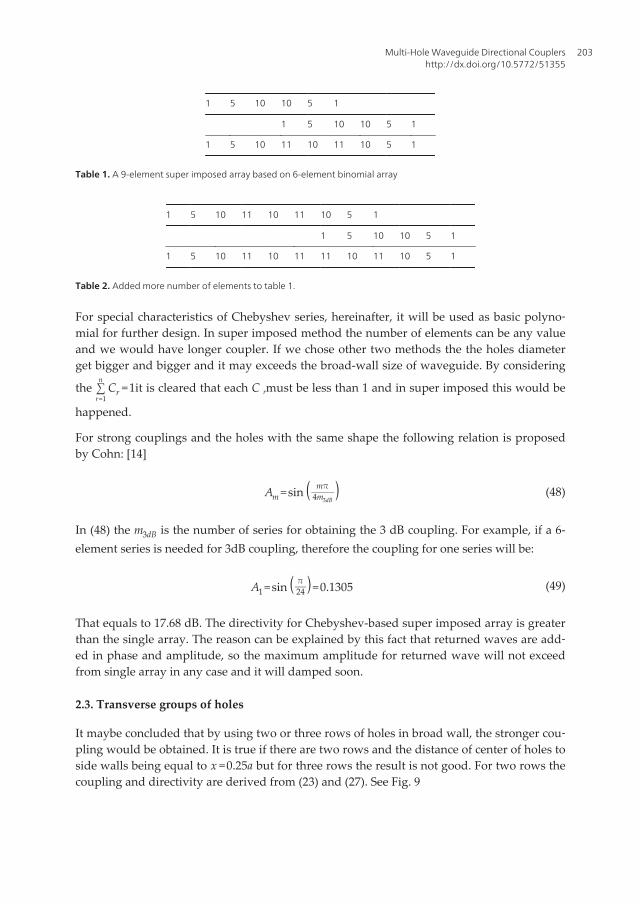
When the strong coupling is needed, i.e. 3dB or 6dB, it is not possible to use the one row ofholes (single array), since diameter of holes will be increased. Therefore it is more conven‐ient to have approximately same diameter for all to get good coupling quality. For this casethe super imposed array is used. As first step, we need the coefficient series in which theholes get bigger. It would be happened when n >4. For starting we can use Chebyshev orbinomial coefficient series in one line. Then the same series should be written in second linebut in shifted position. It means, first coefficient of line 2 in under the 4th coefficient of line 1and so on. By adding the two lines we would have a new series that its coefficients (or holes’diameters) alternately are the same. For example by a 6-element binomial series, we canmake a 9-element super imposed series:
As it has shown, the elements in new series are alternately identical. This can be done byany other number of elements or polynomials. If we wanted to add more number ofholesTable 1, the same way is chosen:
Electromagnetic Waves202
1 5 10 10 5 1
1 5 10 10 5 1
1 5 10 11 10 11 10 5 1
Table 1. A 9-element super imposed array based on 6-element binomial array
1 5 10 11 10 11 10 5 1
1 5 10 10 5 1
1 5 10 11 10 11 11 10 11 10 5 1
Table 2. Added more number of elements to table 1.
For special characteristics of Chebyshev series, hereinafter, it will be used as basic polyno‐mial for further design. In super imposed method the number of elements can be any valueand we would have longer coupler. If we chose other two methods the the holes diameterget bigger and bigger and it may exceeds the broad-wall size of waveguide. By considering
the ∑r=1
nCr =1it is cleared that each C rmust be less than 1 and in super imposed this would be
happened.
For strong couplings and the holes with the same shape the following relation is proposedby Cohn: [14]
Am =sin ( mπ4m3dB
) (48)
In (48) the m3dB is the number of series for obtaining the 3 dB coupling. For example, if a 6-element series is needed for 3dB coupling, therefore the coupling for one series will be:
A1 =sin ( π24 )=0.1305 (49)
That equals to 17.68 dB. The directivity for Chebyshev-based super imposed array is greaterthan the single array. The reason can be explained by this fact that returned waves are add‐ed in phase and amplitude, so the maximum amplitude for returned wave will not exceedfrom single array in any case and it will damped soon.
2.3. Transverse groups of holes
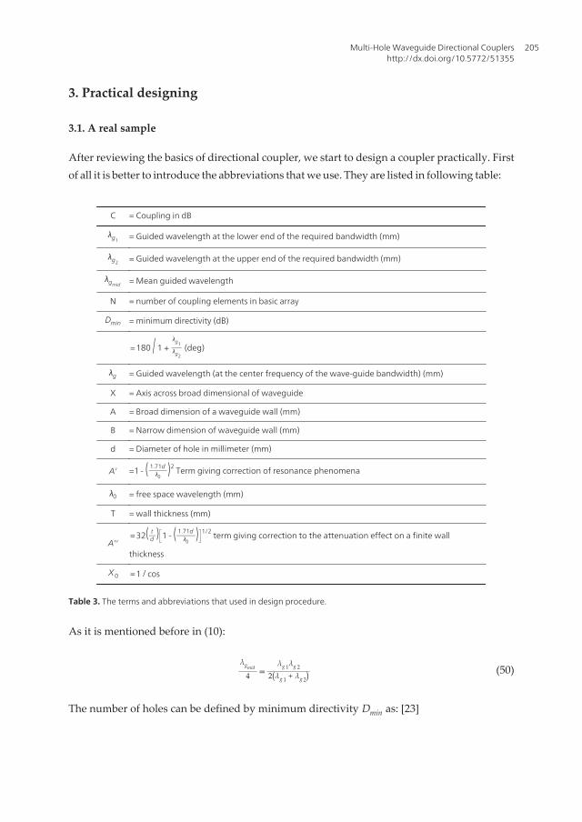
It maybe concluded that by using two or three rows of holes in broad wall, the stronger cou‐pling would be obtained. It is true if there are two rows and the distance of center of holes toside walls being equal to x =0.25a but for three rows the result is not good. For two rows thecoupling and directivity are derived from (23) and (27). See Fig. 9
Multi-Hole Waveguide Directional Couplershttp://dx.doi.org/10.5772/51355
203
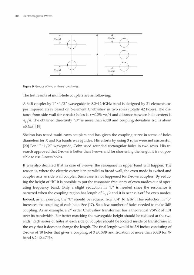
Figure 9. Groups of two or three rows holes.
The test results of multi-hole couplers are as following:
A 6dB coupler by 1 " ×1 / 2" waveguide in 8.2~12.4GHz band is designed by 21-elements su‐per imposed array based on 6-element Chebyshev in two rows (totally 42 holes). The dis‐tance from side-wall for circular-holes is x =0.25a =a / 4 and distance between hole centers isλg / 4. The obtained directivity “D” is more than 40dB and coupling deviation ∆C is about
±0.5dB. [19]
Shelton has tested multi-rows couplers and has given the coupling curve in terms of holesdiameters for X and Ku bands waveguides. His efforts by using 3 rows were not successful.[20] For 1 " ×1 / 2" waveguide, Cohn used rounded rectangular holes in two rows. His re‐search approved that 2-rows is better than 3-rows and for shortening the length it is not pos‐sible to use 3-rows holes.
It was also declared that in case of 3-rows, the resonance in upper band will happen. Thereason is, where the electric vector is in parallel to broad wall, the even mode is excited andcoupler acts as side wall coupler. Such case is not happened for 2-rows couplers. By reduc‐ing the height of “b” it is possible to put the resonance frequency of even modes out of oper‐ating frequency band. Only a slight reduction in “b” is needed since the resonance isoccurred when the coupling region has length of λg / 2 and it is near cut-off for even modes.
Indeed, as an example, the “b” should be reduced from 0.4” to 1/16”. This reduction in “b”increases the coupling of each hole. See (17). So a few number of holes needed to make 3dBcoupling. As an example, a 2nd order Chebyshev transformer has a theoretical VSWR of 1.01over its bandwidth. For better matching the waveguide height should be reduced at the twoends. Each series of holes at each side of coupler should be located inside of transformer inthe way that it does not change the length. The final length would be 3.9 inches consisting of2-rows of 10 holes that gives a coupling of 3 ± 0.5dB and Isolation of more than 30dB for X-band 8.2~12.4GHz.
Electromagnetic Waves204
3. Practical designing
3.1. A real sample
After reviewing the basics of directional coupler, we start to design a coupler practically. Firstof all it is better to introduce the abbreviations that we use. They are listed in following table:
C = Coupling in dB
λg1 = Guided wavelength at the lower end of the required bandwidth (mm)
λg2 = Guided wavelength at the upper end of the required bandwidth (mm)
λgmid = Mean guided wavelength
N = number of coupling elements in basic array
Dmin = minimum directivity (dB)
� = 180 / 1 +λg1λg2
(deg)
λg = Guided wavelength (at the center frequency of the wave-guide bandwidth) (mm)
X = Axis across broad dimensional of waveguide
A = Broad dimension of a waveguide wall (mm)
B = Narrow dimension of waveguide wall (mm)
d = Diameter of hole in millimeter (mm)
A' =1 - ( 1.71dλ0
)2 Term giving correction of resonance phenomena
λ0 = free space wavelength (mm)
T = wall thickness (mm)
A''= 32( t
d ) 1 - ( 1.71dλ0
) 1/2 term giving correction to the attenuation effect on a finite wall
thickness
X0 = 1 / cos �
Table 3. The terms and abbreviations that used in design procedure.
As it is mentioned before in (10):
λgmid
4 =λg 1λg 2
2(λg 1 + λg 2)(50)
The number of holes can be defined by minimum directivity Dmin as: [23]
Multi-Hole Waveguide Directional Couplershttp://dx.doi.org/10.5772/51355
205
n =1 + cosh-1 10Dmin
20
cosh-1 ( 1cos ϕ
) (51)
The starting coefficient in Chebyshev argument is calculated as:
X0 = 1cos ϕ = 1
cos ( 180
1 +
λg1λg2
) (52)
For X-band that we have λg1=6.089 Cm and λg2
=2.489 Cmthe X0 =1.853 is obtained. Next stepis to find the Chebyshev polynomial coefficients by computer program that gives:
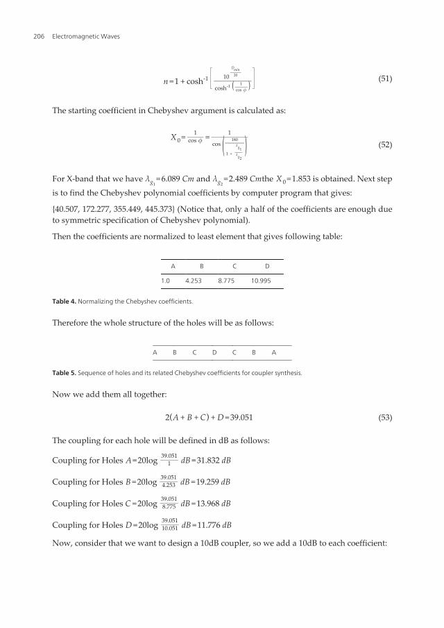
{40.507, 172.277, 355.449, 445.373} (Notice that, only a half of the coefficients are enough dueto symmetric specification of Chebyshev polynomial).
Then the coefficients are normalized to least element that gives following table:
A B C D
1.0 4.253 8.775 10.995
Table 4. Normalizing the Chebyshev coefficients.
Therefore the whole structure of the holes will be as follows:
A B C D C B A
Table 5. Sequence of holes and its related Chebyshev coefficients for coupler synthesis.
Now we add them all together:
2(A + B + C) + D =39.051 (53)
The coupling for each hole will be defined in dB as follows:
Coupling for Holes A=20log 39.0511 dB =31.832 dB
Coupling for Holes B =20log 39.0514.253 dB =19.259 dB
Coupling for Holes C =20log 39.0518.775 dB =13.968 dB
Coupling for Holes D =20log 39.05110.051 dB =11.776 dB
Now, consider that we want to design a 10dB coupler, so we add a 10dB to each coefficient:
Electromagnetic Waves206
CA=41.832 dB, Holes CB=29.259 dB, Holes CC=23.968 dB, Holes CD=21.776 dB
Finally the achieved numbers should be inserted into Bethe’s formula for small size holes: [12]
C =20log { 12a 2bπd 3 1 - ( 1.71d
λ0)2 } + 20log {32( t
d ) 1 - ( 1.71dλ0
) 1/2} (54)
Now we solve the above equation (for each hole) by iteration method and the diameter ofeach hole would be determined. By considering the distance of circle centers to side wall asx =0.203a (7) following values for diameters would be obtained:
A=0.234 inch, B=0.343 inch, C=0.397 inch, D=0.421 inch
Note that the solved example is for single array. If we wanted to have the double rows weshould put the (C+6) dB instead of C dB (that we considered 10 dB in above example).
Notice: an approximation way to define the number of holes “n” is using the Dmin in equalto maximum coupling between holes plus 3 ~ 5 dB. For instance in the solved example, themaximum coupling is belonged to “A” that was C A=41.832 dB. So:
Dmin =CA + 5=47 dB (55)
And the number of holes would be:
n =1 + cosh-1 104720
cosh-1 X 0≈6.9 →n =7 (56)
Therefore if we wanted to have a good directivity, a directivity higher than 47dB then weshould have 7 holes in the coupler.
In practice, for eliminating the effect of wall thickness “t”, it is possible to remove one broadwall of a waveguide and mill- the next wall to have half thickness between to waveguides. [23]
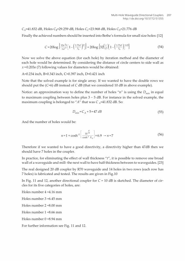
The real designed 20 dB coupler by R70 waveguide and 14 holes in two rows (each row has7 holes) is fabricated and tested. The results are given in Fig.10
In Fig. 11 and 12, another directional coupler for C = 10 dB is sketched. The diameter of cir‐cles for its five categories of holes, are:
Holes number 4 =4.16 mm
Holes number 3 =6.45 mm
Holes number 2 =8.00 mm
Holes number 1 =8.66 mm
Holes number 0 =8.94 mm
For further information see Fig. 11 and 12.
Multi-Hole Waveguide Directional Couplershttp://dx.doi.org/10.5772/51355
207
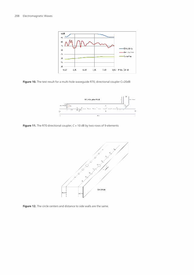
Figure 10. The test result for a multi-hole waveguide R70, directional coupler C=20dB
Figure 11. The R70 directional coupler, C = 10 dB by two rows of 9-elements
Figure 12. The circle centers and distance to side walls are the same.
Electromagnetic Waves208
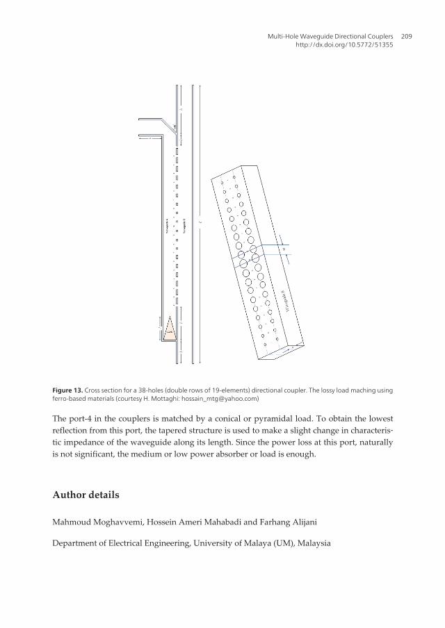
Figure 13. Cross section for a 38-holes (double rows of 19-elements) directional coupler. The lossy load maching usingferro-based materials (courtesy H. Mottaghi: [email protected])
The port-4 in the couplers is matched by a conical or pyramidal load. To obtain the lowestreflection from this port, the tapered structure is used to make a slight change in characteris‐tic impedance of the waveguide along its length. Since the power loss at this port, naturallyis not significant, the medium or low power absorber or load is enough.
Author details
Mahmoud Moghavvemi, Hossein Ameri Mahabadi and Farhang Alijani
Department of Electrical Engineering, University of Malaya (UM), Malaysia
Multi-Hole Waveguide Directional Couplershttp://dx.doi.org/10.5772/51355
209
References
[1] Gandhi, O. P. (1981). Microwave Engineering and Applications, Pergamon Press.
[2] Collin, R. E. (1966). Foundations for Microwave Engineering, Mc. Graw Hill.
[3] Young, Leo. (1966). Advances in Microwave, volume I, Academic Press.
[4] Miller, S. E. (1954). Coupled Wave Theory and Waveguide Applications. Bell systemTech. J., 33, 661.
[5] Riblet, H. J. (1954). The short- slot hybrid Junction. Proc, IRE, 40, 180.
[6] Tomiyasu, K., & Cohn, S. B. (1953). The Transvar Directional Coupler. Proc. IRE, 41,922.
[7] Cook, J. S. (1955). Tapered velocity couplers. Bell system Tech. J., 34, 807-822.
[8] Fox, A. G. (1955). Wave coupling by warped normal modes. Bell System Tech. J., 34,823.
[9] Louisell, W. H. (1955). Analysis of a single tapered mode. Bell System Tech. J., 34, 853.
[10] Miller, S. E., & Mumford, W. W. (1952). Multi-element directional couplers. Proc. IRE,40, 1070.
[11] Bethe, H. A. (1943). Theory of side windows wave guides. Mass. Inst. Technology Radi‐ation Lab Report [43].
[12] Bethe, H. A. (1944). Theory of diffraction by small holes. Phy. Rev. , 66, 163.
[13] Surdin, M. (1946). Directive couplers in wave guides. J. Inst. Elec. Engrs (London) ,93(IIIA), 725.
[14] Cohn, S. B., Knootz, R. H. S., & Wehn, S. L. (1962). Microwave hybrid coupler studyprogram. Rantec- Corporation Report [61], 361-363.
[15] Cohn, S. B. (1952). Microwave coupling by large aperture. Proc IRE, 40, 697.
[16] Levy, R. H. (1959). Guide to the practical application of Chebyshev functions to thedesign of microwave components. Proc. Inst. Elec. Engrs. (London) C, 106, 193.
[17] Harrison, J. R. (1945). Design considerations for directional couplers. MIT RadiationLab. Rept. [724].
[18] Saad, T. (1964). The Microwave Engineers handbook. 109 Boston, Massachusetts.
[19] Hensperger, E. S. (1959). The design of multi-hole coupling arrays. Microwave J., 2, 38.
[20] Shelton, W. (1961). Compact multi-hole waveguide directional couplers. Microwave J.,4, 89.
[21] Geranpaye. (1985). Waveguide standards. ITRC, Tehran, Iran.
Electromagnetic Waves210
[22] Alison, W. B. W. A. (1987). A handbook for the mechanical tolerance of waveguidecomponents. Artech house.
[23] Hancock, K. E. (1967). The design and manufacture of waveguide Tchebyshev direc‐tional-coupler. Electron. Eng , 39, 292.
[24] Liang, C. H., & Cheng, D. K. (1982). On performance limitations of aperture couplingbetween rectangular waveguide. MTT-30 [5].
[25] Levy, R. (1968). Analysis and synthesis of waveguide multi-aperture directional cou‐plers. MTT-16 [12].
[26] Mc Donald, N. A. (1972). Electric and Magnetic coupling through small apertures inshield wall of any thickness. MTT-20 [10].
[27] Levy, R. (1980). Improved single and multi- aperture waveguide coupling theory in‐cluding explanation of mutual interactions. MTT-28 [4].
[28] Riblet, H. J. (1947). A Mathematical theory of differential coupler. Proc. IRE, 35, 1307.
[29] Crompton, J. W. (1957). A contribution to the design of multi-element directionalcouplers. Proc. IEE, 104C(6TD), 398-402.
[30] Matthaei, G. L. (1964). Microwave Filters impedance matching networks and couplingstructures, Mc Graw Hill.
[31] Wheeler, H. A. (1964). Coupling holes between resonant cavities or waveguides eval‐uation terms of volume ratios. MTT, 231.
[32] Sangster, A. J. (1973). Slot Coupling between uniform rectangular waveguides.MTT-27 [7], 705.
[33] Pandhuri, Pande. V. H., & Das, B. W. (1979). comments on coupling of waveguidesthrough large aperture. MTT-27 [7], 702.
[34] Pandhuri, Pande. V. H., & Das, B. W. (1978). coupling of waveguide through largeaperture. MTT-26 [3], 209.
[35] Schmiedel, H., & Arndt, F. (1986). Field Theory Design of Rectangular WaveguideMultiple-Slot Narrow-Wall couplers. MTT-34 [7], 791.
[36] Oliner, A. H. (1960). Equivalent circuits for small symmetrical longitudinal apertureand obstacles, . IRE MTT, 72.
[37] Hakkak, M., & Barakat, F. (1984). Waveguide bend characteristics. ITRC publication‐sTehran, Iran.
[38] Mottaghi, H. (2010). Measuring the Load absorption parameters in waveguide.IT&mmwaves SDN BHD, Kuala Lumpur.
Multi-Hole Waveguide Directional Couplershttp://dx.doi.org/10.5772/51355
211

Electromagnetic Waves212
![WIDEBAND MULTILAYER DIRECTIONAL COUPLER WITH …...One group of such circuits consists of microstrip directional couplers with distributed coupling [1], which have gained signif-icant](https://img.pdfslide.net/doc/110x75/604134904496467b0c5379a9/wideband-multilayer-directional-coupler-with-one-group-of-such-circuits-consists.jpg)


![A Novel Design of A Microstrip 3dB Coupler - IJMOT · 2014. 10. 27. · CST Microwave Studio [8]. II. THEORICAL STUDY OF COUPLERS Couplers called “Branch-Line” as shown in fig.1,directional](https://img.pdfslide.net/doc/110x75/60d36a9adab8a71c382a93d2/a-novel-design-of-a-microstrip-3db-coupler-ijmot-2014-10-27-cst-microwave.jpg)