Embed Size (px)
Citation preview
DEPARTMENT OF TECHNOLOGY AND BUILT ENVIRONMENT
Multidimensional Measurements
on RF Power Amplifiers
Hibah Al Tahir
September 2008
Master’s Thesis
Master Program in Electronics / Telecommunications
Examiner: Magnus Isaksson
Supervisor: Niclas Björsell

Acknowledgement I would Like to thank Dr. Niclas Björsell – the project supervisor- for his continuous
guidance and support. Thanks are extended to my project partner Edith Condo and our
co-supervisor Charles Nader for their help.
I am deeply appreciative of my family for their endless love, care and support.
I am also grateful to my colleagues Efrain Zenteno , Per Landin and Ahsan Azhar for
the fruitful discussions and the friendly environment in the Lab.
i
Abstract
In this thesis, a measurement system was set to perform comprehensive measurements
on RF power amplifiers. Data obtained from the measurements is then processed
mathematically to obtain three dimensional graphs of the basic parameters affected or
generated by nonlinearities of the amplifier i.e. gain, efficiency and distortion .Using a
class AB amplifier as the DUT, two sets of signals – both swept in power level and
frequency - were generated to validate the method, a two-tone signal and a WCDMA
signal. The three dimensional plot gives a thorough representation of the behavior of the
amplifier in any arbitrary range of spectrum and input level. Sweet spots are
consequently easy to detect and analyze. The measurement setup can also yield other
three dimensional plots of variations of gain, efficiency or distortion versus frequencies
and input levels. Moreover, the measurement tool can be used to plot traditional two
dimensional plots such as, input versus gain, frequency versus efficiency etc, making the
setup a practical tool for RF amplifiers designers.
The test signals were generated by computer then sent to a vector signal generator that
generates the actual signals fed to the amplifier. The output of the amplifier is fed to a
vector signal analyzer then collected by computer to be handled. MATLAB® was used
throughout the entire process.
The distortion considered in the case of the two-tone signals is the third order
intermodulation distortion (IM3) whereas Adjacent Channel Power Ratio (ACPR) was
considered in the case of WCDMA.
ii
Table of Contents:
Chapter 1: Introduction 1.1 Introduction
1.2 Measurements of RF amplifiers
1.3 Classes of Amplifiers
1.4 Class AB amplifiers
1.5 LDMOS Technology
1.6 Thesis Outline
Chapter 2: Theory 2.1 Introduction
2.2 Test Signals
2.2.1 Two-tones Signals
2.2.2 WCDMA
2.3 Distortion 2.3.1 Third Order Intermodulation Products
2.3.2 Adjacent channel power ratio
2.3.3 Memory Effects
2.4 Gain
2.5 Efficiency
2.6 Sampling Theorem
2.6.1 Coherent Sampling
2.7 Fast Fourier Transform (FFT)
2.8 Correlation
2.9 Geometric Representation of Modulated Signals
Chapter 3: Method 3.1 Introduction
3.2 Test Setup
9 9
9
10
11
12
13
14 14
14
14
15
16
16
17
17
17
18
18
19
19
20
20
22 22
22
iii
3.3 System Operation
3.4 Signal Generation
3.4.1 Two-tone signals 3.4.2 WCDMA
3.5 DUT
3.6 Data collection and synchronization
3.6.1 Two-tone Signals
3.6.2 WCDMA
3.7 Current Measurements
3.8 Asymmetry Chapter 4: Results 4.1 Introduction
4.2 Graphical User Interface (GUI)
4.3 Two-tone Measurements
4.4 WCDMA Measurements
4.5 Measurement Time
Chapter 5: Discussion and conclusions 5.1 System Capabilities and Limitations
5.2 Future Work
References
23
23
23
24
26
26
26
26
27
28
29 29
30
31
34
39
40 40
41
42
iv
List of Abbreviations
2-D
3-D
ACLR
ACPR
BW
DC
DFT
DLL
DUT
ETSI
FFT
GSM
GUI
GPIB
IM3
LDMOS
PA
PAE
PAR
PEP
PRBS
R&S
RF
SDSSS
VSA
VSG
WCDMA
Two Dimensional
Three Dimensional
Adjacent Channel Leakage Ratio
Adjacent Channel Power Ratio
Bandwidth
Direct Current
Discrete Fourier Transform
Dynamic Link Library
Device Under Test
European Telecommunication Standards Institute
Fast Fourier Transform
Global System for Mobile communications
Graphical User Interface
General Purpose Interface Bus
Third Order Inter-modulation Distortion
Lateral Double-Diffused MOSFET
Power Amplifier
Power Added Efficiency
Peak to Average Ratio
Peak Envelope Power
Pseudo Random Binary Sequence
Rohde and Schwarz ®
Radio Frequency
Selectable Direct Sequence Spread Spectrum
Vector Spectrum Analyzer
Vector Signal Generator
Wideband Code Division Multiple Access
v
List of Figures Fig 1.1: 1 dB Compression point
Fig 1.2: 1.2 (a) Waveforms of ideal PAs
1.2 (b) Conduction areas of different PA classes
Fig 1.3: A classic schematic of class AB amplifier
Fig 1.4: Schematic cross section for LDMOS technology
Fig 2.1: WCDMA signal
Fig 2.2: IQ modulator
Fig 3.1: Test setup
Fig 3.2: A 14 power-step two-tone signal at 2.14GHz with Δf= 250 KHz
Fig 3.3: Magnitude transfer function of a raised cosine filter.
Fig 3.4: Current waveform in two-tone measurements
Fig 4.1: GUI of the project
Fig 4.2: GUI with modified markers
Fig 4.3: Efficiency versus gain versus IM3_high
Fig 4.4 : Frequency versus input power versus efficiency
Fig 4.5: Frequency versus input power versus gain
Fig 4.6: Input power versus output power(legend ≡ tones GHz)
Fig 4.7: Efficiency versus gain versus ACPR_High (dBC)
Fig 4.8: WCDMA carriers versus input power versus gain
Fig 4.9 : WCDMA carrier versus input power versus efficiency
Fig 4.10: WCDMA carrier versus efficiency (legend ≡ input power in dB)
Fig 4.11: Efficiency versus gain versus ACPR_High (dBC)
Fig 4.12: WCDMA carriers versus input power versus gain
Fig 4.13 : WCDMA carrier versus input power versus efficiency
vi
List of Tables Table 4.1: List of figures that can be plotted by the system
Table 4.2: Test conditions ( two-tone )
Table 4.3: Test conditions (WCDMA)
Table 4.4: Test conditions (WCDMA)
vii
Chapter 1
Introduction 1.1 Introduction This project was conducted in partnership with Edith Graciela Condo as a part of a
master thesis [1]. The main objectives of the project are to implement a user friendly
measurement system that is capable of performing measurements on RF power amplifiers
and plotting gain, efficiency, and distortion in three dimensions. Then analyze the
amplifier under test based on the results of the measurements. Finally, implement a
graphical user interface for commonly used applications of the measurement system.
The motive to the project is to give a better visualization to the amplifier behavior.
Designers usually have measurement results in the form of tables. Even though tables are
informative, they do not give the visualization provided by figures. Other merits of the
method are ease of measurements and time efficiency. The user specifies the
measurement boundaries in terms of frequency and power levels then obtain a full set of
measurement results about the amplifier in a relatively short time . Sweet spots can also
be detected easily in three dimensional graphs.
This chapter will give a general background on RF amplifiers, amplifiers classes, the
technology used for the transistor under test (LDMOS) and the thesis outline. 1.2 Measurements of RF amplifiers Characterization of RF power amplifiers has always been a challenge for RF
engineers. Several parameters are significant when characterizing an amplifier; however,
some parameters are commonly of interest. Efficiency, for example, is an important
parameter of an amplifier, however, to obtain the maximum efficiency the amplifier is
usually pushed into its non-linear region. This, in turn, induces intermodulation products.
The non linear region is the region where the gain of the amplifier does not increase
linearly with the increment of the input. One common measure of nonlinearity is the 1dB
compression point. The 1dB compression point, as the name implies, is the point where
the signal gain has dropped 1 dB [2]. Figure 1.1 illustrates 1 dB compression point.
1
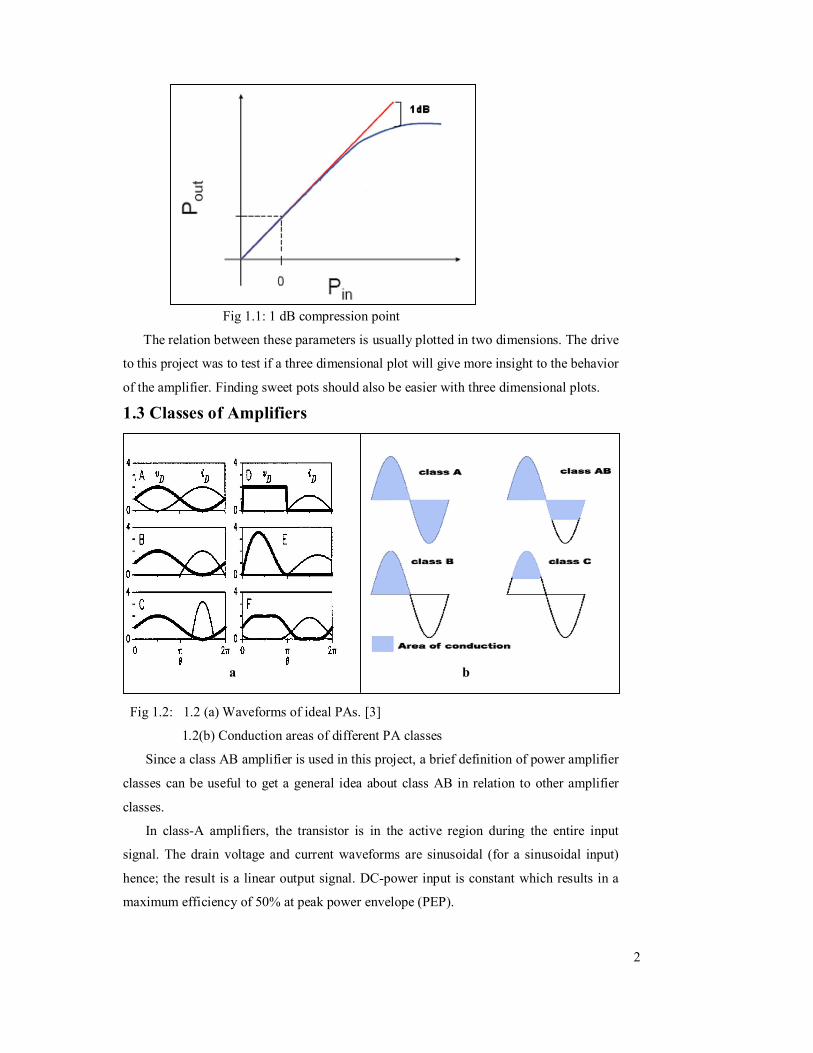
Fig 1.1: 1 dB compression point
The relation between these parameters is usually plotted in two dimensions. The drive
to this project was to test if a three dimensional plot will give more insight to the behavior
of the amplifier. Finding sweet pots should also be easier with three dimensional plots.
1.3 Classes of Amplifiers
Fig 1.2: 1.2 (a) Waveforms of ideal PAs. [3]
1.2(b) Conduction areas of different PA classes Since a class AB amplifier is used in this project, a brief definition of power amplifier
classes can be useful to get a general idea about class AB in relation to other amplifier
classes.
In class-A amplifiers, the transistor is in the active region during the entire input
signal. The drain voltage and current waveforms are sinusoidal (for a sinusoidal input)
hence; the result is a linear output signal. DC-power input is constant which results in a
maximum efficiency of 50% at peak power envelope (PEP).
a b
2
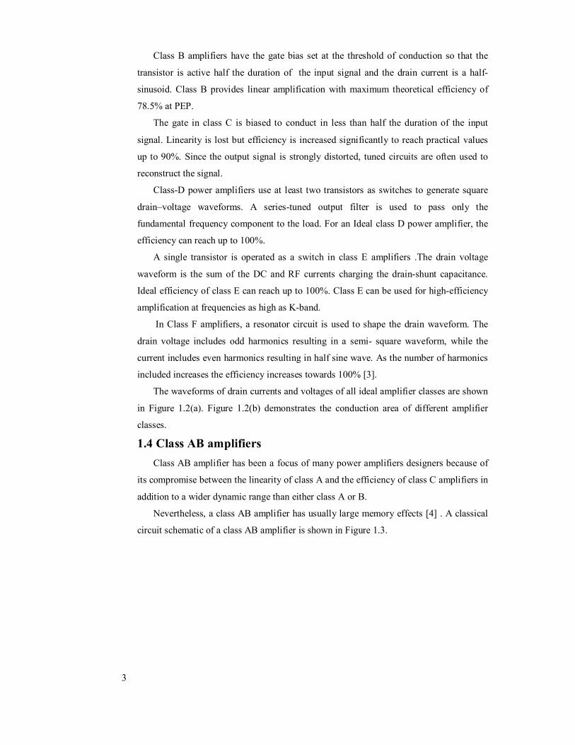
Class B amplifiers have the gate bias set at the threshold of conduction so that the
transistor is active half the duration of the input signal and the drain current is a half-
sinusoid. Class B provides linear amplification with maximum theoretical efficiency of
78.5% at PEP.
The gate in class C is biased to conduct in less than half the duration of the input
signal. Linearity is lost but efficiency is increased significantly to reach practical values
up to 90%. Since the output signal is strongly distorted, tuned circuits are often used to
reconstruct the signal.
Class-D power amplifiers use at least two transistors as switches to generate square
drain–voltage waveforms. A series-tuned output filter is used to pass only the
fundamental frequency component to the load. For an Ideal class D power amplifier, the
efficiency can reach up to 100%.
A single transistor is operated as a switch in class E amplifiers .The drain voltage
waveform is the sum of the DC and RF currents charging the drain-shunt capacitance.
Ideal efficiency of class E can reach up to 100%. Class E can be used for high-efficiency
amplification at frequencies as high as K-band.
In Class F amplifiers, a resonator circuit is used to shape the drain waveform. The
drain voltage includes odd harmonics resulting in a semi- square waveform, while the
current includes even harmonics resulting in half sine wave. As the number of harmonics
included increases the efficiency increases towards 100% [3].
The waveforms of drain currents and voltages of all ideal amplifier classes are shown
in Figure 1.2(a). Figure 1.2(b) demonstrates the conduction area of different amplifier
classes.
1.4 Class AB amplifiers Class AB amplifier has been a focus of many power amplifiers designers because of
its compromise between the linearity of class A and the efficiency of class C amplifiers in
addition to a wider dynamic range than either class A or B.
Nevertheless, a class AB amplifier has usually large memory effects [4] . A classical
circuit schematic of a class AB amplifier is shown in Figure 1.3.
3
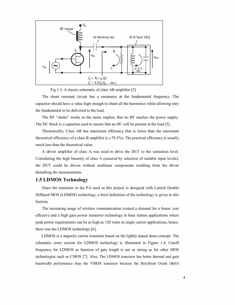
Fig 1.3: A classic schematic of class AB amplifier [5]
The shunt resonant circuit has a resonance at the fundamental frequency .The
capacitor should have a value high enough to shunt all the harmonics while allowing only
the fundamental to be delivered to the load.
The RF “choke” works as the name implies, that no RF reaches the power supply.
The DC block is a capacitor used to ensure that no DC will be present at the load [5].
Theoretically, Class AB has maximum efficiency that is lower than the maximum
theoretical efficiency of a class B amplifier (i.e.78.5%). The practical efficiency is usually
much less than the theoretical value.
A driver amplifier of class A was used to drive the DUT to the saturation level.
Considering the high linearity of class A (ensured by selection of suitable input levels),
the DUT could be driven without nonlinear components resulting from the driver
disturbing the measurements.
1.5 LDMOS Technology Since the transistor in the PA used in this project is designed with Lateral Double
Diffused MOS (LDMOS) technology, a brief definition of the technology is given in this
Section.
The increasing usage of wireless communication created a demand for a linear, cost
effective and a high gain power transistor technology in base station applications where
peak power requirements can be as high as 120 watts in single carrier applications; hence,
there was the LDMOS technology [6].
LDMOS is a majority carrier transistor based on the lightly doped drain concept. The
schematic cross section for LDMOS technology is illustrated in Figure 1.4. Cutoff
frequency for LDMOS as function of gate length is not as strong as for other MOS
technologies such as CMOS [7]. Also, The LDMOS transistor has better thermal and gain
bandwidth performance than the VMOS transistor because the Beryllium Oxide (BeO)
4
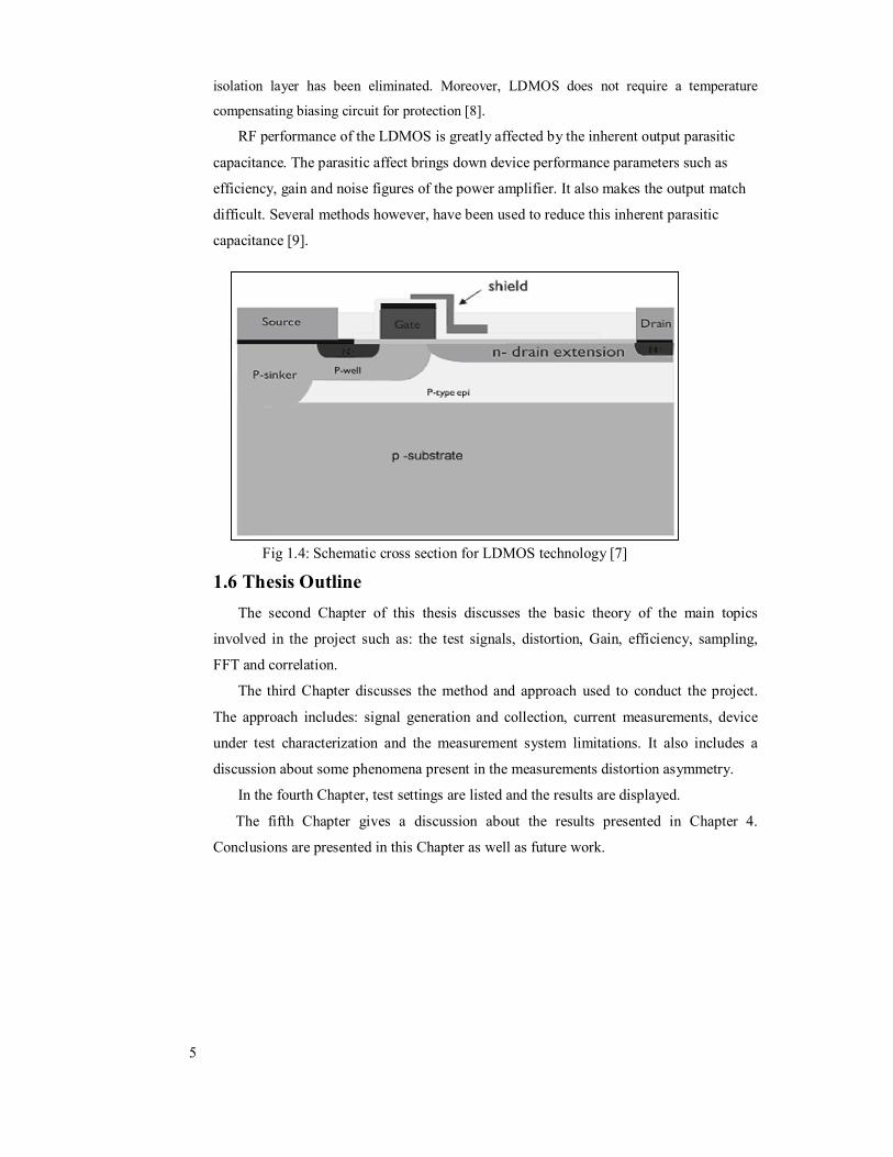
isolation layer has been eliminated. Moreover, LDMOS does not require a temperature
compensating biasing circuit for protection [8].
RF performance of the LDMOS is greatly affected by the inherent output parasitic
capacitance. The parasitic affect brings down device performance parameters such as
efficiency, gain and noise figures of the power amplifier. It also makes the output match
difficult. Several methods however, have been used to reduce this inherent parasitic
capacitance [9].
Fig 1.4: Schematic cross section for LDMOS technology [7]
1.6 Thesis Outline The second Chapter of this thesis discusses the basic theory of the main topics
involved in the project such as: the test signals, distortion, Gain, efficiency, sampling,
FFT and correlation.
The third Chapter discusses the method and approach used to conduct the project.
The approach includes: signal generation and collection, current measurements, device
under test characterization and the measurement system limitations. It also includes a
discussion about some phenomena present in the measurements distortion asymmetry.
In the fourth Chapter, test settings are listed and the results are displayed.
The fifth Chapter gives a discussion about the results presented in Chapter 4.
Conclusions are presented in this Chapter as well as future work.
5
Chapter 2
Theory 2.1 Introduction Several parameters can be considered when characterizing an RF power amplifier. In
a class AB amplifier, nonlinear operation is usually of interest. Consequently,
characteristics of non-linear operation such as distortion, gain reduction and efficiency
improvement are to be studied. In this Chapter these parameters will be discussed
theoretically along with some other parameters and functions addressed in the project;
e.g. memory effects, coherent sampling and Fourier transform.
2.2 Test Signals The simplest yet very informative stimulus to characterize nonlinearities in non-
linear devices is the two-tone signal. Such kind of characterization is becoming
increasingly important for evaluating different aspects of nonlinearity such as in-band
distortion or spectral re-growth [10].
2.2.1 Two-tones Signals A multi-tone signal is represented as:
1
( ) sin( )N
k k kk
u t a t
(2.1)
Where ka are the amplitudes, k are the angular velocity with 0< N < and k are
the phases.
To obtain a signal with only the positive frequencies, u (t) is multiplied with the unit
step.
( ) 2 ( ) ( )stepU f U f U f (2.2)
The time domain representation of equation (2.2) is:
2( ) ( ) j ftu t U f e df
6
1 12 ( ) * 2 ( )stepF U f F U f (2.3)
Where 1F is the inverse Fourier transform. Hence,
( ) ( ) * ( )ju t t u tt
1( ) * ( )u t j u tt
(2.4)
The second term of equation (2.4) is equivalent to the Hilbert transform of u (t).
Then the low pass equivalent of signal u (t) is: 2( ) ( ) cj f tu t u t e
( ) ( )I t jQ t (2.5)
Where I(t) is the in phase component and Q(t) is the quadrature phase Components.
To summarize the two tone signal generation: it is the low pass equivalent of the
summation of the signal u (t) and its Hilbert transform [11].
2.2.2 WCDMA Wide Code Division Multiple Access (WCDMA) is a 3G standard that employs
selectable direct sequence spread spectrum (SDSSS) technique and has been designed for
an (always –on) packet based wireless condition. WCDMA supports a packet data rate of
2.048 Mbps per user. Therefore, allowing effective sound and multimedia traffic.
WCDMA requires 5 MHz of spectrum which is much higher than GSM; making
changes in base stations RF equipment inevitable. Using such a wide channel enables
WCDMA to have bit rates up to 2Mbps and carry simultaneously 100-350 voice calls
depending on antenna sectoring, antenna polarization, propagation conditions and user
velocity. The SDSSS chip rate of WCDMA can exceed 16 Mchips per second per user. A
rule of thumb that WCDMA provides at least a six times increase in spectral efficiency
over GSM compared on a system wide basis [12].
True WCDMA includes a number of embedded messages corresponding to the
number of users served by the channel which is not easy to generate in the lab. Therefore,
it is common to generate WCDMA either by generating a multiple tones signal or a noise
like signals that have the same properties of a true WCDMA signal.
In case of the multiple tones, the signal is generated with equal tone spacing and can
be represented as: 1
( )
0
( ) k k
Nj t
kk
s t A e
(2.6)
Where N is the number of samples , kA is the amplitude, k is the frequency and k is
the phase.
7
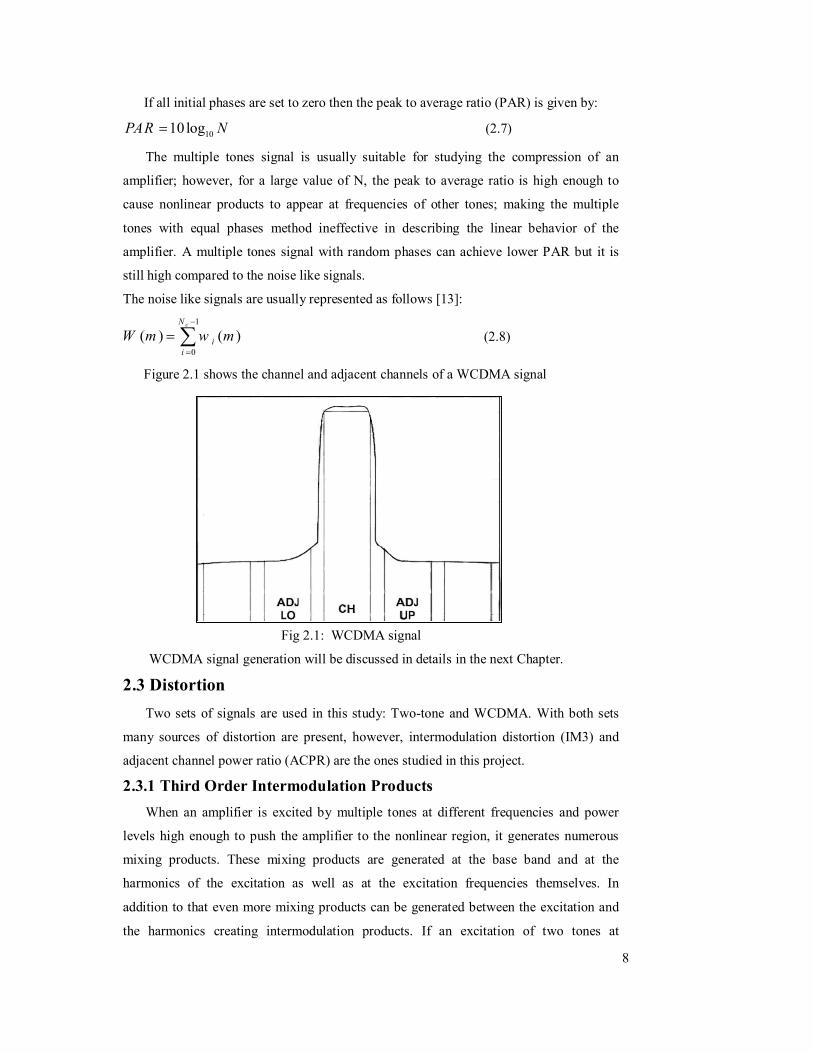
If all initial phases are set to zero then the peak to average ratio (PAR) is given by:
1010logPAR N (2.7)
The multiple tones signal is usually suitable for studying the compression of an
amplifier; however, for a large value of N, the peak to average ratio is high enough to
cause nonlinear products to appear at frequencies of other tones; making the multiple
tones with equal phases method ineffective in describing the linear behavior of the
amplifier. A multiple tones signal with random phases can achieve lower PAR but it is
still high compared to the noise like signals.
The noise like signals are usually represented as follows [13]: 1
0
( ) ( )cN
ii
W m w m
(2.8)
Figure 2.1 shows the channel and adjacent channels of a WCDMA signal
Fig 2.1: WCDMA signal
WCDMA signal generation will be discussed in details in the next Chapter.
2.3 Distortion Two sets of signals are used in this study: Two-tone and WCDMA. With both sets
many sources of distortion are present, however, intermodulation distortion (IM3) and
adjacent channel power ratio (ACPR) are the ones studied in this project.
2.3.1 Third Order Intermodulation Products When an amplifier is excited by multiple tones at different frequencies and power
levels high enough to push the amplifier to the nonlinear region, it generates numerous
mixing products. These mixing products are generated at the base band and at the
harmonics of the excitation as well as at the excitation frequencies themselves. In
addition to that even more mixing products can be generated between the excitation and
the harmonics creating intermodulation products. If an excitation of two tones at
8
frequencies f1 and f2 is applied to an amplifier then the third order intermodulation
products will occur at 2f1-f2 and 2f2-f1. The designation of “ third order” comes form a
common representation of the transfer function of the amplifier as a simple power series;
where the third term arises from gain compression and includes the frequencies 2f1-f2
and 2f2-f1 [14].
A detailed mathematical description of the IM3 distortion can be found in [14], [15].
2.3.2 Adjacent channel power ratio Adjacent channel power ratio (also referred to as Adjacent Channel Leakage Ratio
(ACLR)) is a distortion usually associated with WCDMA signals. ACPR is defined as the
ratio between total linear power in one channel and the total linear power leaking from
the adjacent channel. The ACPR is referred to as upper ACPR if the leakage is from the
upper adjacent channel and lower ACPR if the leakage s from the lower adjacent channel.
The ETSI specifies that the ACLR should not be below 45dB within 5 MHz below
the first or above the last carrier frequency [15].
2.3.3 Memory Effects Memory effects are usually introduced by changes made in bandwidth of the input
signal. If two-tones are introduced to an amplifier, the difference between the frequencies
represents the bandwidth of the signal and therefore, memory effects are present when a
two-tone signal is applied [16].
2.4 Gain When designing an amplifier, the gain can be represented in several ways, such as
transducer power gain, power gain and available power gain. The equations for these
gains are given below [17]:
LTransducer
AV S
PGP
(2.9)
_L
Power GainIN
PGP
(2.10)
_AVN
Available GainAVS
PGP
(2.11)
Where is the power delivered to the loadLP is the power available from the sourceA VSP is input to the network INP the power from the networkA VNP is
As the equations show, the transducer gain is the ratio between the power delivered to
the load and the power available from the source. Whereas the power gain is the ratio
between the power delivered to the load and the input power the network. The available 9
gain is the ratio between the power provided by the supply and the power at the input of
the amplifier.
In this project only the power gain is of interest. A driver amplifier is used to obtain
power high enough to push the DUT to compression. The gain of the system will be a
combination of the gains of the two amplifiers. If the driver has an impulse response of
H1(ω) and the DUT has an impulse response of H2(ω) then the total gain of the system
H(ω) is equal to H1(ω)*H2(ω) in the linear scale . This is equivalent to H1(ω)dB+H2dB(ω)
in logarithmic scale.
2.5 Efficiency Obtaining the maximum efficiency of power amplifiers is a major goal for RF
amplifiers engineers. In order to meet the linearity requirements, the amplifier is usually
backed off. This causes the efficiency to drop drastically i.e. there is always a trade-off
between efficiency and linearity [16].
Three definitions of efficiency are commonly used. Drain efficiency, power added
efficiency and instantaneous efficiency. Drain efficiency is defined as: ratio of RF-output
power to DC-input power. Mathematically, drain efficiency is defined as:
_/out in DCEFF P P . (2.12)
Whereas Power Added Efficiency (PAE) is defined the difference between the output
power and the input power divided over the DC input power, PAE is given by:
_( ) /out in in DCPAE P P P (2.13)
PAE can be negative for very low gains. The instantaneous efficiency represents the
efficiency at every instant of time. The highest instantaneous efficiency will occur at the
peak of the input [3].
2.6 Sampling Theorem The Sampling theorem basically states that the analog signal to be sampled should be
sampled at a rate at least twice its highest frequency component. If this condition is
satisfied, then the analog signal can be reconstructed from the sampled signal. In practice,
the original signal can not be exactly recovered from the sampled signal due to the fact
that the sinc function (sin ωt / ωt) is infinite. Nevertheless, the analog signal can still be
recovered with acceptable accuracy.
For a signal with restricted bandwidth a special exception of the sampling theorem
can be applied so that the signal can be sampled at a rate equal to the difference between
the highest frequency component and the lowest frequency component. E.g. if a signal
has a band of f1<f<f2, the minimum sampling frequency can be reduced from 2f2 to the
10
rate f2-f1, which is the bandwidth of the signal. The exception is only applicable if the
samples are generated as in-phase and quadrature-phase components
In practical applications a low pass filter (commonly called an anti-aliasing filter) is
used ahead of the digitizer to eliminate under sampling. Since the ideal rectangular cutoff
characteristics are unrealizable, the sampling rate is usually chosen to be even higher than
twice the highest frequency component of the analog signal. Over sampling also
eliminated the need for sophisticated interpolation techniques in most of the cases,
making the reconstruction of the signal much easier [18].
In addition to satisfying the sampling theorem, coherent sampling should be applied.
2.6.1 Coherent Sampling Coherent sampling is a method of sampling periodic signals where the sampling
window fits an integer number of full periods of the periodic signal. Mathematically,
coherent sampling is expressed as:
in
s
f Nf M
(2.14)
Where, inf : Frequency of the periodic input signal.
sf : Sampling frequency. M : Number of cycles within the sampling window ( should be an odd integer). N : Number of points in the sampling window and is a power of two.
Coherent sampling provides higher spectral resolution when used with FFT.
According to IEEE standard 1057 : “For an ideal transfer characteristic in the absence
of random noise, the minimum record sue that will ensure a representative sample of
every code bin is 2π M2, with the following restriction: The input frequency is chosen
such that the number of cycles per record is an integer that is prime relative to M so that
there are no common factors ” [19].
2.7 Fast Fourier Transform (FFT) The basic idea behind all fast algorithm computation of discrete Fourier transform is
to divide the sequence into smaller segments and perform the discrete time Fourier
transform (DFT) on them. FFT provides reduction in the computation complexity. FFT is
used in this project to extract the frequencies of the input tones from the signal received
from the spectrum analyzer. Detailed explanation of FFT and DFT can be found in [20].
11
2.8 Correlation Correlation is used in this project to compare and synchronize the input signal to the
collected signal. Assume a pair of signals x[n] and y[n]. The cross correlation is given by:
[ ] [ ] [ ], 0, 1, 2,...xyr l x n y n l l
(2.15)
Where l is the lag, and represents the time shift between the pair. If l is positive then y[n]
is said to be shifted by l samples to the right of x[n] and to the left of x[n] if l is negative.
The ordering of x[n] and y[n] indicates that x[n] is the reference signal. If y[n] was
taken as the reference, then the correlation is given by:
[ ] [ ] [ ], 0, 1, 2,... [ ]yx xyr l y n x n l l r l
(2.16)
Therefore, [ ]yxr l is obtained by reversing the sequence [ ]xyr l in time [20].
2.9 Geometric Representation of Modulated Signals If a modulation signal set S includes M possible waveforms then S can be
represented as:
1 2( ), ( ),.............., ( )MS s t s t s t (2.17)
If the elements of S are viewed as points of vector space, then from a geometric point
of view, any finite set of physically realizable waveforms in a vector space can be
expressed as a linear combination of N orthonormal forms which forms the basis of that
vector space. If a signal is to be represented in the vector space, then the signals that form
the basis of the vector space must be found. Once that is done, any point in that vector
space can be represented as a combination of the basis signals ( ), 1,2,.......,j t j N
such that [12]:
1
( ) ( )N
i ij jj
s t s t
(2.18)
The basis signals are orthogonal to one another in time such that:
( ) ( ) 0,i jt t dt i j
(2.19)
Each of the basis signals is normalized to have unit energy i.e.
2 ( ) 1iE t dt
(2.20)
Since a binary modulation scheme is used in this project, the binary information bit is
mapped directly to the signal.
12
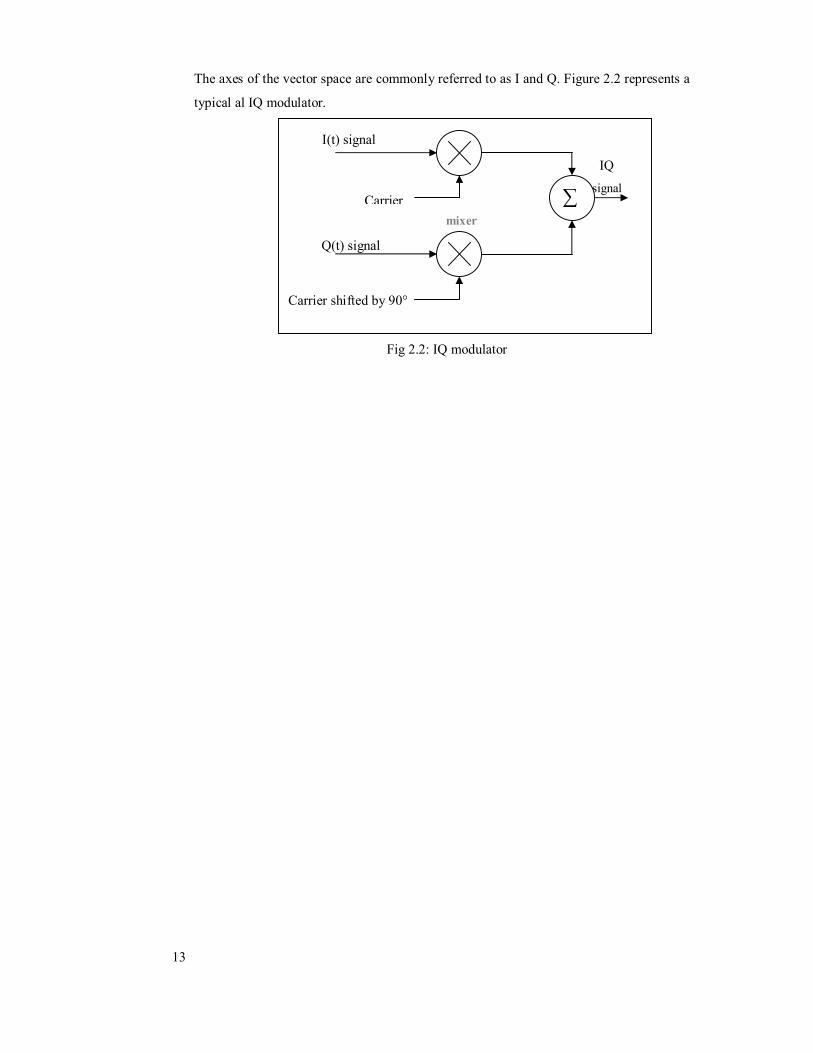
The axes of the vector space are commonly referred to as I and Q. Figure 2.2 represents a
typical al IQ modulator.
Fig 2.2: IQ modulator
mixer
IQ signal
Q(t) signal
Carrier shifted by 90°
∑
Carrier
I(t) signal
13
Chapter 3
Method 3.1 Introduction The project involved different stages with several methods. The device under test was
a class AB amplifier and the whole test setup was in a 50 ohm environment. To drive the
DUT, a driver of class A was used. MATLAB® was utilized to handle all the
communication with the vector signal generator (VSG) and the vector spectrum analyzer
(VSA) through GPIB port. An oscilloscope was used to measure the drain current. The
test signals and all the mathematical computations were handled in MATLAB®.
In this Chapter, the setup of the project is explained in details as well as the data
collection and processing.
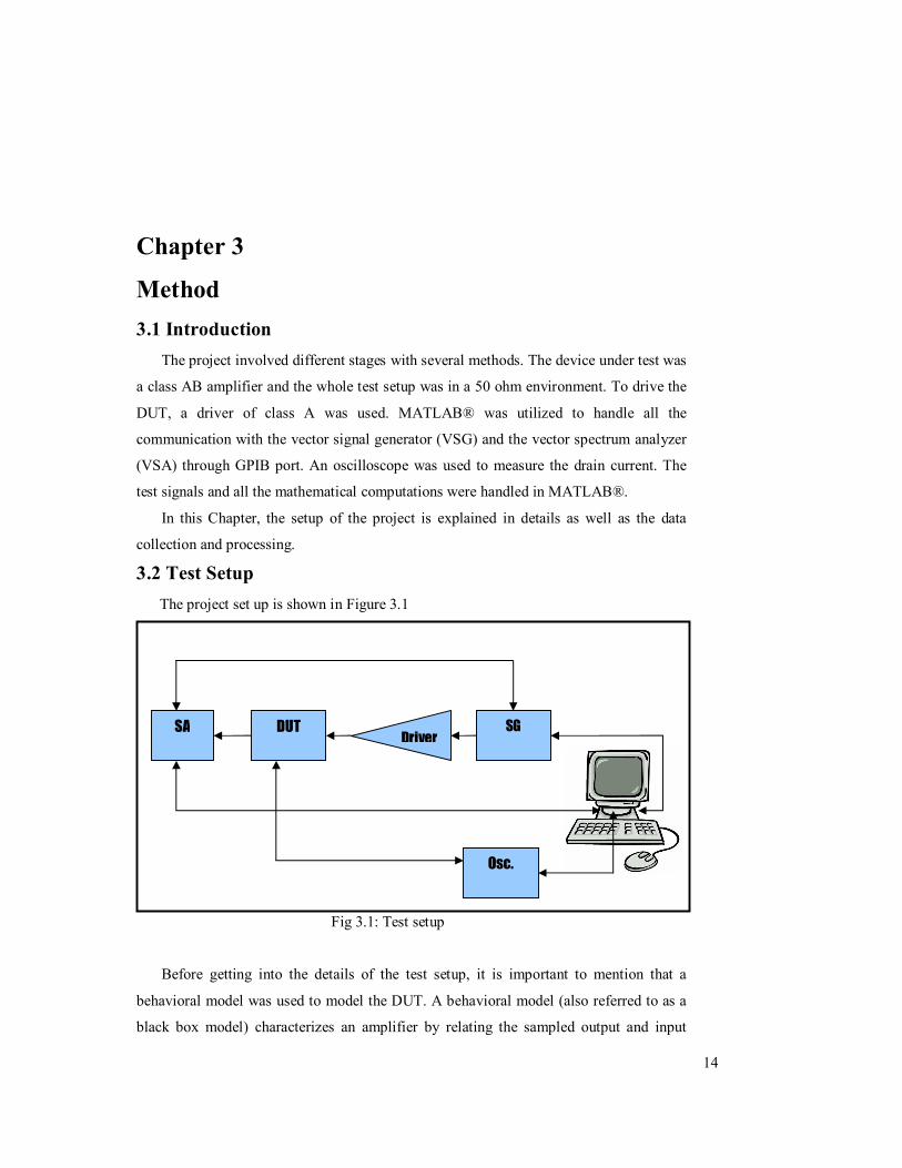
3.2 Test Setup The project set up is shown in Figure 3.1
Fig 3.1: Test setup
Before getting into the details of the test setup, it is important to mention that a
behavioral model was used to model the DUT. A behavioral model (also referred to as a
black box model) characterizes an amplifier by relating the sampled output and input
DUT SA SG
Osc.
Driver
14
signals and can effectively characterize the nonlinearities and memory effects in an
amplifier [21].
3.3 System Operation The system is expected to work with basically any RF PA. The user should specify
the frequency range, number of frequency steps, the input power levels range and the
power steps size. The step size defines the rate at which the power or frequency are to be
swept.
3.4 Signal Generation This Section describes the generation of the test tones used in the project and the
practical limitations of generation. Two types of signals were used in this project to
validate the method: two-tone and WCDMA signals. The method should be applicable to
any kind of signal since it is universal, however, changes in the code might be required to
handle other types of signals. In both cases of two-tone and WCDMA, the data was sent
as I-Q data (for more details about I-Q modulation see Section 2.9).
As mentioned before, a class A driver was used to provide the DUT with adequate
input power level. The gain of the driver (47.3 dB), was later compensated for in the
characterization of the DUT.
3.4.1 Two-tone signals Both test signals were generated initially in MATLAB® then R&S® SMU200A
vector signal generator was used to generate the actual RF power. The center frequency
was 2.14 GHz with sampling frequency of 40 MHz. The maximum measurable range of
frequency around the carrier is 9MHz due to the limitation of IQ bandwidth of the vector
spectrum analyzer. An IQ bandwidth of 28MHz was used giving the possibility to
measure in a range of 14 MHz at each side of the carrier. Since the IM3 products are to be
measured, calculations showed that the maximum allowable frequency should not exceed
9 MHz (i.e. 4.5 MHz at each side of the carrier) e.g. if a range of 9 MHz is set, the
highest IM3 frequency is calculated as follows (2*4.5MHz-(-4.5MHz))= 13.5MHz which
is still covered with the IQ bandwidth. However, changing the carrier frequency enables
measurements on any arbitrary range of the spectrum.
The two-tone baseband signals where generated in such a way that only the positive
frequencies are present. The user then specifies the ranges of frequency and power as
well as the steps. The result from this specification is a set of two-tone pairs in blocks.
Each block contains all the power levels (in steps) of a specific two-tone frequency pair.
Coherent sampling was used to ensure higher spectral resolution (i.e. avoiding
spectral leakage), therefore, the tones spacing can be slightly different (within tens of
Hertz).
15
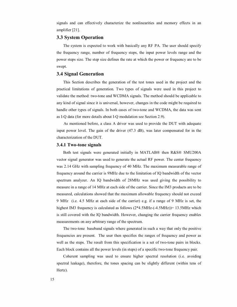
Special attention should be paid when setting the power levels of the two-tone
signals. First, a reference level is set at the signal generator. All the power levels are
calculated in relation to that reference level e.g. if the reference level is set to -4 dB and
the power level is set to -5, then the power at the signal generator is -4-5=-9dB.
Since the power set in MATLAB® refers to the average power, the peak power will
always be 3dB (since the two tones generated are of equal amplitude and zero phase
difference)
Referring the previous example, the -9 will be the average power and the peak will be
-6dB.
Figure 3.2 shows a 14 power-step two-tone signal at 2.14GHz with Δf= 250 KHz.
Fig 3.2: A 14 power-step two-tone signal at 2.14GHz with Δf= 250 KHz
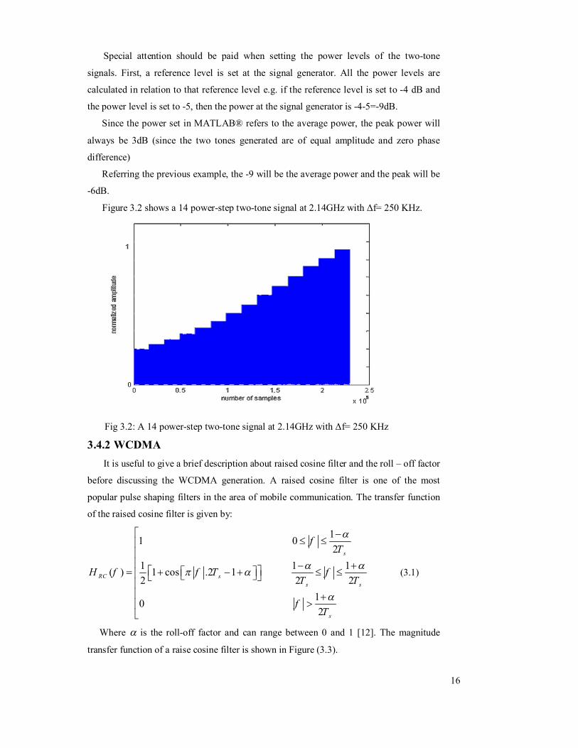
3.4.2 WCDMA It is useful to give a brief description about raised cosine filter and the roll – off factor
before discussing the WCDMA generation. A raised cosine filter is one of the most
popular pulse shaping filters in the area of mobile communication. The transfer function
of the raised cosine filter is given by:
11 02
1 1 1( ) 1 cos .2 1 2 2 2
10 2
s
RC ss s
s
fT
H f f T fT T
fT
(3.1)
Where is the roll-off factor and can range between 0 and 1 [12]. The magnitude
transfer function of a raise cosine filter is shown in Figure (3.3).
16
Fig 3.3: Magnitude transfer function of a raised cosine filter.
A true WCDMA signal consists of a number of embedded message signals
corresponding to the number of users which is not practical to generate in the lab. It is
easier to generate a noise like signal that bears the same shape and characteristics of a
true WCDMA signal and behaves in the same way. This noise-like signal is first
generated by summing up a number of pseudo random Binary sequence (PRBS) of
length M . The number of PRBS is selected to represent different users of the system.
Mathematically: 1
0
( ) ( )cN
ii
W m w m
(3.2)
Where cN is the number of PSBS and m is the chip number, 1, 2,........ 1m M .
The sequence is then clipped to achieve a certain peak to average ratio (PAR). The
clipped sequence is then applied to root raised cosine filter with an over sampling ratio of
R and a roll-off factor of 0.22 as specified for WCDMA. The final signal has a length of
*M R and a sampling frequency of *R C , where C is the chip rate and is equal to 63.84*10 as specified for WCDMA [13] .
WCDMA specifications require that the ACPR should be measured 5MHz below the
first and above the last carrier used . Therefore, only one WCDMA signal could be sent
to the amplifier at a time due to the limitation of the IQ bandwidth of the VSA. I.e. since
the IQ bandwidth of the VSA is 28 MHz, then with a WCDMA signal having a band of
3.84 MHz and another 5MHz at each side for the ACPR measurements, there is not
enough range to measure another WCDMA signal.
The user specifies the range of frequency to be measured and the frequency step size
as well as the input power range and the power step size. The frequencies generated will
represent the carrier frequencies of the WCDMA signals. For each carrier frequency, the
entire specified power range will be swept in steps and each power step will be sent
17
separately to the amplifier. The reference level of the VSG will be set individually for
every power level. This yields more time consumption compared to two-tone
measurements. The power levels set by the user are the actual power levels to be sent to
the amplifier. Again, these power levels represent the average power levels. PAR in the
generated WCDMA signals is 10 dB therefore; the peak value is always 10 dB higher
than the average values.
3.5 DUT DUT is a class AB amplifier provided by freescale semiconductor®. The amplifier is
a single stage amplifier and the transistor is implemented using LDMOS technology. The
transistor (freescale® MRF7S21150H) operates at 28V drain voltage and 5.33V gate
voltage. The quiescent drain current is 1.35A. The amplifier has a gain of 17.5 dB at
2.14GHz and its return loss at the same frequency is -40dB.
3.6 Data collection and synchronization
3.6.1 Two-tone Signals Data collected from the VSA is in I-Q form. If a sequence of N samples is sent to the
VSA, then at least 2N must be collected to ensure that at least one full sequence will
start at the beginning of the first step. To be able to extract that full sequence, the
collected data is correlated to the sent signal. Correlation is used to detect the point at
which the received signal is most similar to the sent signal. That point has the highest
value in the correlation result. The desired signal is then extracted from the received
sequence using the highest value of the correlation as the starting point. Once that is
done, FFT is then applied to the correlated data to get its spectral representation. The FFT
will give the spectral representation of the entire band covered with the IQ bandwidth,
However, only four points are of interest: the two-tones and their third order
intermodulation products. Hence, these four points are located and their corresponding
power levels are recorded.
3.6.2 WCDMA Data is also collected in the form of I-Q modulated signals. The procedure is quite
similar to collecting two-tone signals with few exceptions. First, there is no need for
synchronization since the spectrum represents a single signal. Also, the definition of
distortion has changed; now it should be the average of distortion in the channels above
and below the carrier. To cover that channel, a Hanning window is used. The loss of
energy due to the Hanning window is compensated for by adding the energy of the same
Hanning window (i.e. same length) to the data.
18
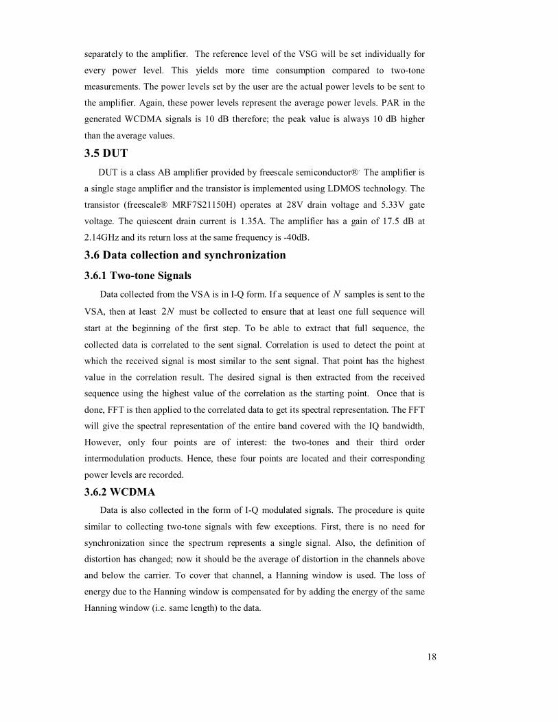
3.7 Current Measurements The Drain current of the amplifier is needed to calculate the power added efficiency.
Current measurements were performed using Agilent® 54610B digitizing
oscilloscope. The oscilloscope has a bandwidth of 500 MHz and sampling rate of
20MHz/second. Agilent® current probe N2783A was used with the oscilloscope. The
probe measurements appear in the oscilloscope screen as voltage where each volt
represents 10 Amperes.
0 100 200 300 400 500 600 700 8000
0.1
0.2
0.3
0.4
0.5
0.6
0.7
0.8
0.9
1
Samples
Nor
mal
ized
Am
plitu
de
Current Waveform
Fig 3.4: Current waveform in two-tone measurements
The current measurement method differs slightly depending on the test signal. In the
case of two-tone, the accuracy of current measurement depends strongly on the choice of
the number of samples per power step ( N ).
In order to view the current corresponding to each power step, N should be large to
provide enough time for the current to settle before rising to the next level. If N is too
small, the current will appear as a straight line instead of the correct current waveform
( shown in Figure 3.4).
19
Nevertheless, N can not be chosen to be unlimitedly large, since higher number of
samples yields more computation time and usage of memory.
The choice of N is also affected by the tone spacing. The narrower the tone spacing,
the higher the N needed to measure the current correctly.
The number of samples that achieved the best compromise between the above
mentioned criteria was found to be 142N , which is relatively high. With 142N the
total number of samples sent per a power sweep is given by the multiplication of the
number of power steps by the number of samples per power step i.e. the number of
steps*N .
Due to a limitation in the software used to collect the data, the number of samples to
be collected from the VSA was limited to 500000 samples. Combining this limitation
with the choice of suitable N, the maximum number of steps allowed per two-tones was
15.
The oscilloscope was set to get the average of 8 measurements before sending the
readings. The next task was to precisely extract one full sweep starting from the lowest
step to the highest. A code was implemented to extract the required sequence. Each value
of the current was recorded with its corresponding power step.
In the case of WCDMA, current measurements were simpler since the data collected
each time corresponds to a single WCDMA signal. The oscilloscope data was read and
the average of the readings was taken and recorded.
3.8 Asymmetry Asymmetry in amplitude of lower and upper IM3 is often observed in microwave
power amplifiers subject to two-tone or multitone stimulus. In case A WCDMA signal is
applied, the asymmetry appears as a difference between the power level of the lower
adjacent channel and the higher adjacent channel.
Asymmetry in general is a result of memory effects in the power amplifier. Several
methods attribute the asymmetry to different kinds of memory effects e.g. biasing
network , variations of low-frequency output impedance, out of band terminations,
limitation of the modulation bandwidth, unbalance in two input signal drive level and
thermal time constants of the power amplifier [22],[23].
20
Chapter 4
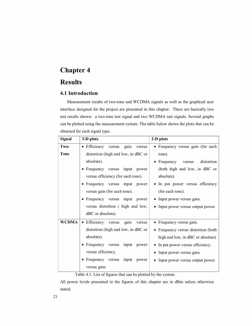
Results 4.1 Introduction Measurement results of two-tone and WCDMA signals as well as the graphical user
interface designed for the project are presented in this chapter. There are basically two
test results shown: a two-tone test signal and two WCDMA test signals. Several graphs
can be plotted using the measurement system. The table below shows the plots that can be
obtained for each signal type.
Signal 3-D plots 2-D plots
Two-
Tone
Efficiency versus gain versus
distortion (high and low, in dBC or
absolute).
Frequency versus input power
versus efficiency (for each tone).
Frequency versus input power
versus gain (for each tone).
Frequency versus input power
versus distortion ( high and low,
dBC or absolute).
Frequency versus gain (for each
tone).
Frequency versus distortion
(both high and low, in dBC or
absolute).
In put power versus efficiency
(for each tone).
Input power versus gain.
Input power versus output power.
WCDMA Efficiency versus gain versus
distortion (high and low, in dBC or
absolute).
Frequency versus input power
versus efficiency.
Frequency versus input power
versus gain.
Frequency versus gain.
Frequency versus distortion (both
high and low, in dBC or absolute)
In put power versus efficiency.
Input power versus gain.
Input power versus output power.
Table 4.1: List of figures that can be plotted by the system
All power levels presented in the figures of this chapter are in dBm unless otherwise
stated.
21
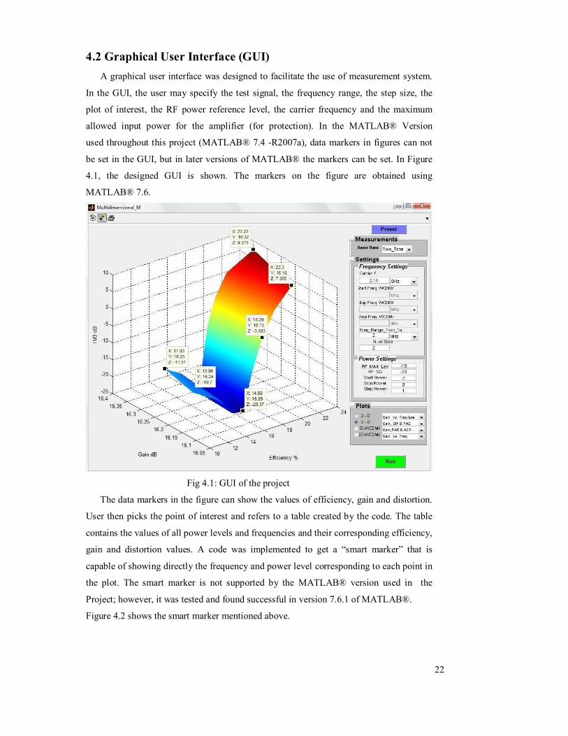
4.2 Graphical User Interface (GUI) A graphical user interface was designed to facilitate the use of measurement system.
In the GUI, the user may specify the test signal, the frequency range, the step size, the
plot of interest, the RF power reference level, the carrier frequency and the maximum
allowed input power for the amplifier (for protection). In the MATLAB® Version
used throughout this project (MATLAB® 7.4 -R2007a), data markers in figures can not
be set in the GUI, but in later versions of MATLAB® the markers can be set. In Figure
4.1, the designed GUI is shown. The markers on the figure are obtained using
MATLAB® 7.6.
Fig 4.1: GUI of the project
The data markers in the figure can show the values of efficiency, gain and distortion.
User then picks the point of interest and refers to a table created by the code. The table
contains the values of all power levels and frequencies and their corresponding efficiency,
gain and distortion values. A code was implemented to get a “smart marker” that is
capable of showing directly the frequency and power level corresponding to each point in
the plot. The smart marker is not supported by the MATLAB® version used in the
Project; however, it was tested and found successful in version 7.6.1 of MATLAB®.
Figure 4.2 shows the smart marker mentioned above.
22
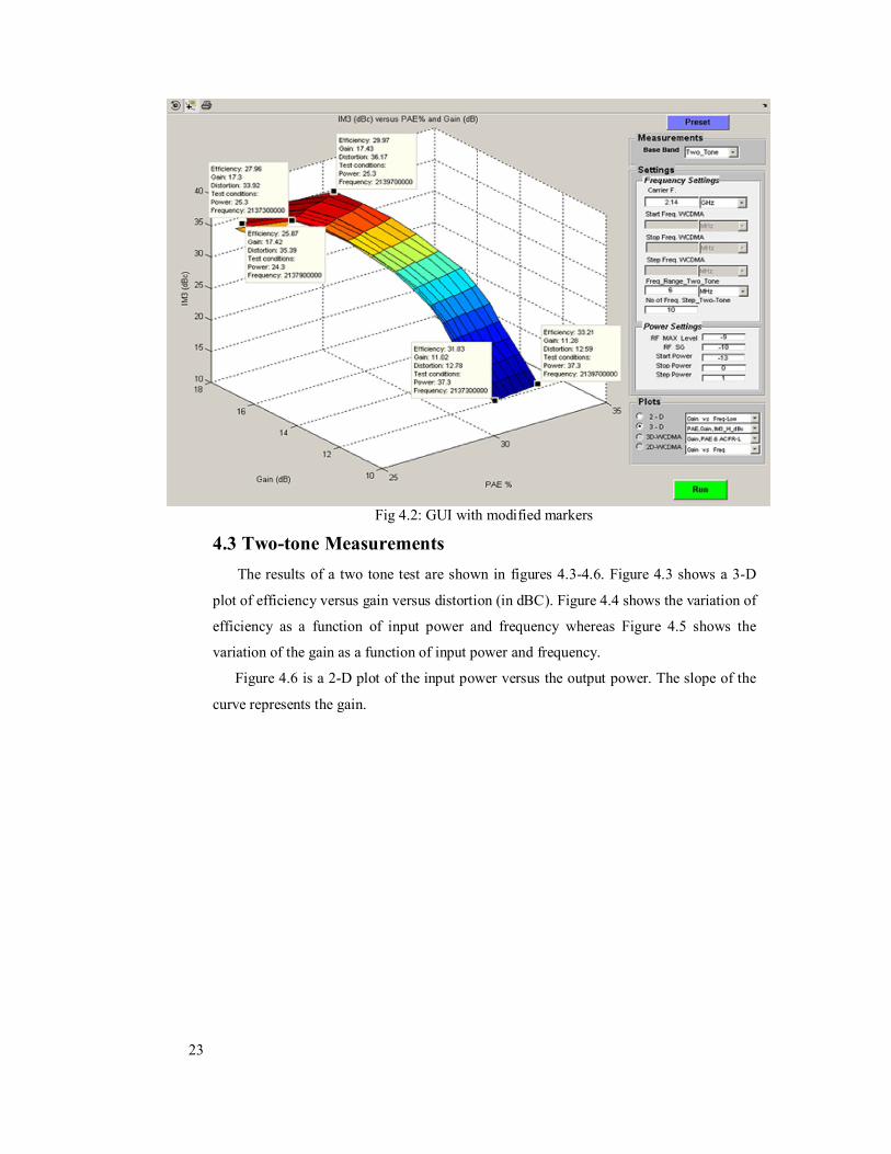
Fig 4.2: GUI with modified markers
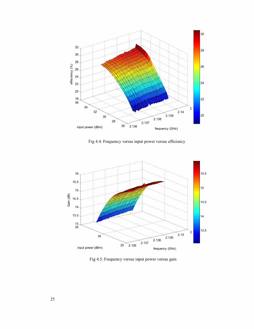
4.3 Two-tone Measurements The results of a two tone test are shown in figures 4.3-4.6. Figure 4.3 shows a 3-D
plot of efficiency versus gain versus distortion (in dBC). Figure 4.4 shows the variation of
efficiency as a function of input power and frequency whereas Figure 4.5 shows the
variation of the gain as a function of input power and frequency.
Figure 4.6 is a 2-D plot of the input power versus the output power. The slope of the
curve represents the gain.
23
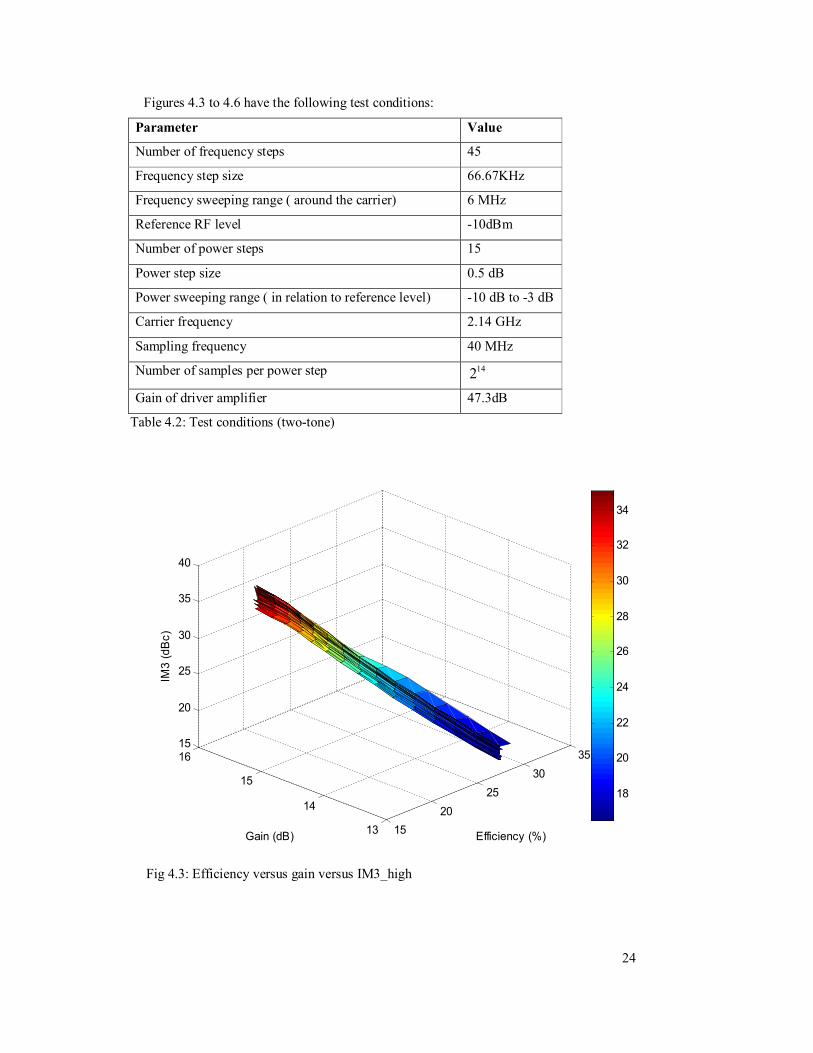
Figures 4.3 to 4.6 have the following test conditions:
Parameter Value
Number of frequency steps 45
Frequency step size 66.67KHz
Frequency sweeping range ( around the carrier) 6 MHz
Reference RF level -10dBm
Number of power steps 15
Power step size 0.5 dB
Power sweeping range ( in relation to reference level) -10 dB to -3 dB
Carrier frequency 2.14 GHz
Sampling frequency 40 MHz
Number of samples per power step 142
Gain of driver amplifier 47.3dB
Table 4.2: Test conditions (two-tone)
1520
2530
35
13
14
15
1615
20
25
30
35
40
Efficiency (%)Gain (dB)
IM3
(dB
c)
18
20
22
24
26
28
30
32
34
Fig 4.3: Efficiency versus gain versus IM3_high
24
2.1362.137
2.1382.139
2.142.141
2628
3032
343618
20
22
24
26
28
30
32
frequency (GHz)input power (dBm)
effe
cien
cy (%
)
20
22
24
26
28
30
Fig 4.4: Frequency versus input power versus efficiency
2.1362.137
2.1382.139
2.142.141
25
30
3513
13.5
14
14.5
15
15.5
16
frequency (GHz)input power (dBm)
Gai
n (d
B)
13.5
14
14.5
15
15.5
Fig 4.5: Frequency versus input power versus gain
25
27 28 29 30 31 32 33 34 3542
43
44
45
46
47
48
Input power levels to DUT (dBm)
outp
ut p
ower
(dB
m)
2.13992.13992.13982.13972.13972.13962.13952.13952.13942.13932.13932.13922.13912.1391 2.1392.13892.13892.13882.13872.13872.13862.1385
Fig 4.6: Input power versus output power (legend ≡ tones GHz)
4.4 WCDMA Measurements For WCDMA, there is no limitation on the number of power steps or frequency
steps since a single WCDMA signal is sent to the amplifier at each step. Two test results
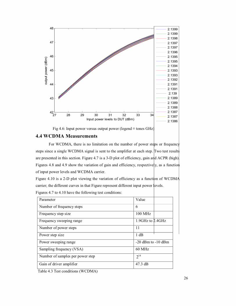
are presented in this section. Figure 4.7 is a 3-D plot of efficiency, gain and ACPR (high).
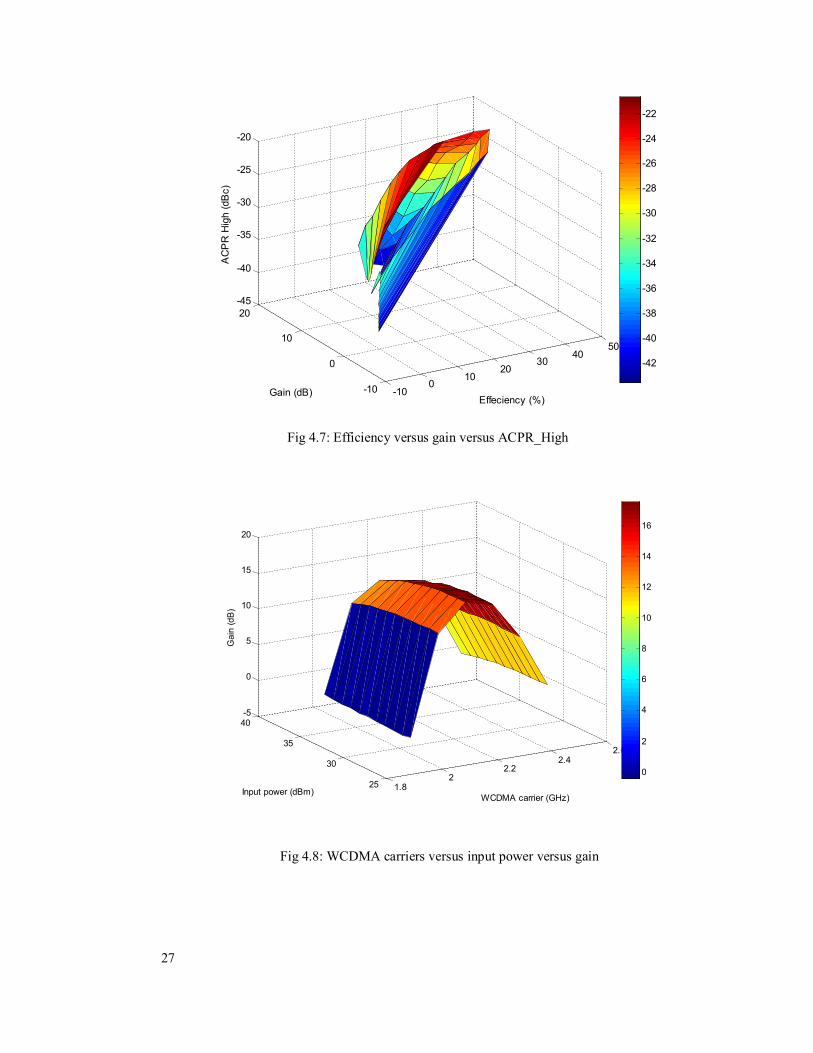
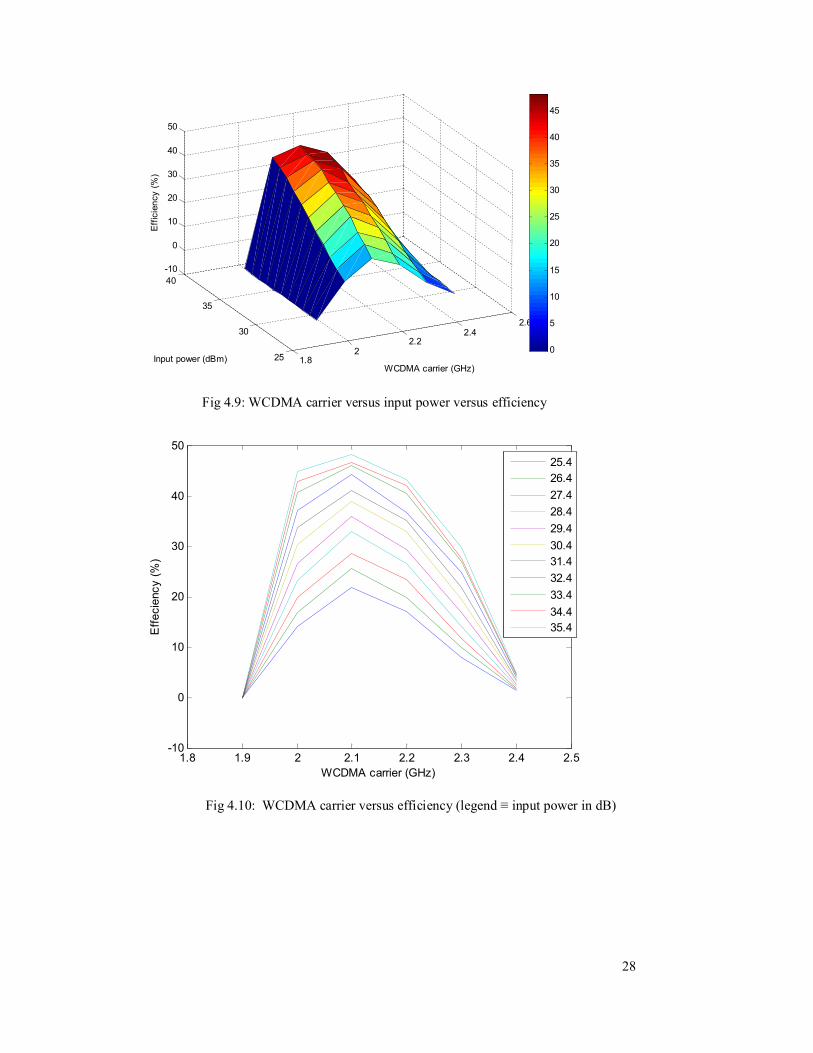
Figures 4.8 and 4.9 show the variation of gain and efficiency, respectively, as a function
of input power levels and WCDMA carrier.
Figure 4.10 is a 2-D plot viewing the variation of efficiency as a function of WCDMA
carrier; the different curves in that Figure represent different input power levels.
Figures 4.7 to 4.10 have the following test conditions:
Parameter Value
Number of frequency steps 6
Frequency step size 100 MHz
Frequency sweeping range 1.9GHz to 2.4GHz
Number of power steps 11
Power step size 1 dB
Power sweeping range -20 dBm to -10 dBm
Sampling frequency (VSA) 60 MHz
Number of samples per power step 142
Gain of driver amplifier 47.3 dB
Table 4.3 Test conditions (WCDMA)
26
-100
1020
3040
50
-10
0
10
20-45
-40
-35
-30
-25
-20
Effeciency (%)Gain (dB)
AC
PR
Hig
h (d
Bc)
-42
-40
-38
-36
-34
-32
-30
-28
-26
-24
-22
Fig 4.7: Efficiency versus gain versus ACPR_High
1.82
2.22.4
2.6
25
30
35
40-5
0
5
10
15
20
WCDMA carrier (GHz)Input power (dBm)
Gai
n (d
B)
0
2
4
6
8
10
12
14
16
Fig 4.8: WCDMA carriers versus input power versus gain
27
1.82
2.22.4
2.6
25
30
35
40-10
0
10
20
30
40
50
WCDMA carrier (GHz)Input power (dBm)
Effi
cien
cy (%
)
0
5
10
15
20
25
30
35
40
45
Fig 4.9: WCDMA carrier versus input power versus efficiency
1.8 1.9 2 2.1 2.2 2.3 2.4 2.5-10
0
10
20
30
40
50
WCDMA carrier (GHz)
Effe
cien
cy (%
)
25.426.427.428.429.430.431.432.433.434.435.4
Fig 4.10: WCDMA carrier versus efficiency (legend ≡ input power in dB)
28
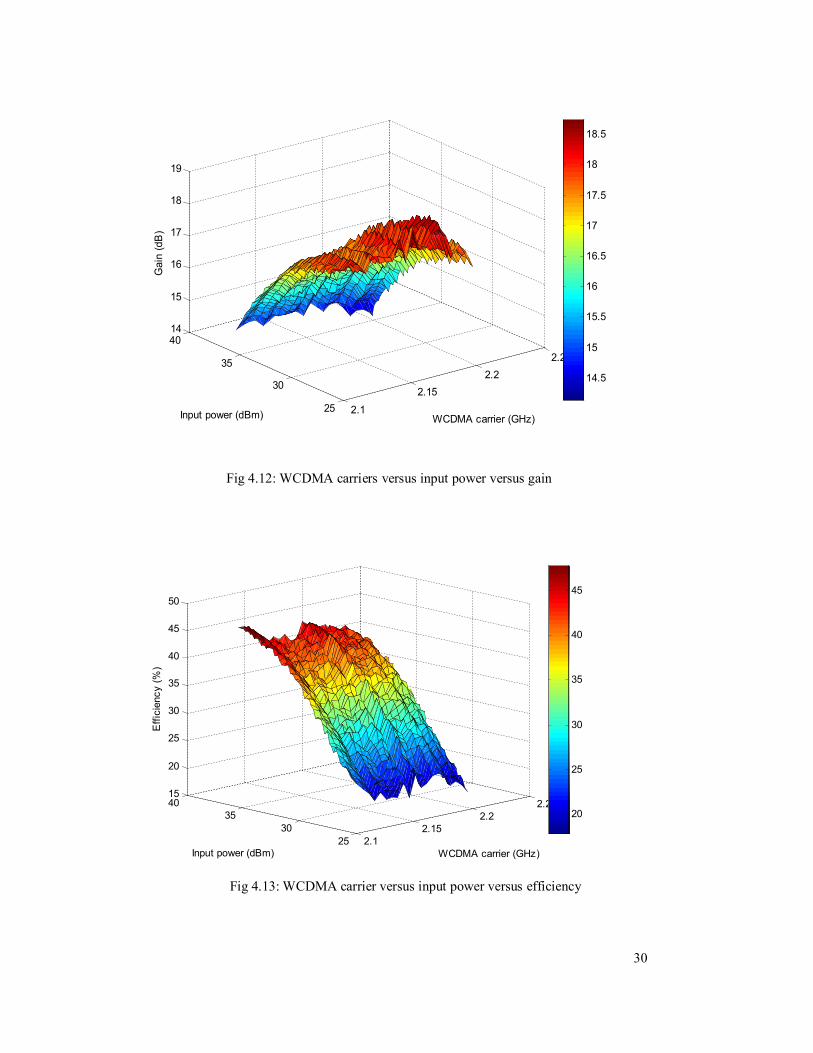
Figures 4.11 to 4.13 are the results of another WCDMA measurement with more
power and frequency steps under the following test conditions:
Parameter Value
Number of frequency steps 21
Frequency step size 5 MHz
Frequency sweeping range 2.1GHz to 2.2GHz
Number of power steps 51
Power step size 0.2 dB
Power sweeping range -20 dBm to -10 dBm
Sampling frequency (VSA) 60 MHz
Number of samples per power step 142
Gain of driver amplifier 47.3 dB
Table 4.4: Test conditions (WCDMA)
Figure 4.11 shows a 3-D plot of efficiency versus gain versus distortion of the
WCDMA signal. The gain of the signal under various input power levels and with
different carriers is shown in Figure 4.12. Figure 4.13 represents the efficiency of the
signal as a function of input power level and carrier variations.
1020
3040
50
1415
1617
1819-45
-40
-35
-30
-25
-20
Effeciency (%)Gain (dB)
AC
PR
Hig
h (d
Bc)
-42
-40
-38
-36
-34
-32
-30
-28
-26
-24
-22
Fig 4.11: Efficiency versus gain versus ACPR_High
29
2.1
2.152.2
2.25
25
30
35
4014
15
16
17
18
19
WCDMA carrier (GHz)Input power (dBm)
Gai
n (d
B)
14.5
15
15.5
16
16.5
17
17.5
18
18.5
Fig 4.12: WCDMA carriers versus input power versus gain
2.12.15
2.22.25
2530
354015
20
25
30
35
40
45
50
WCDMA carrier (GHz)Input power (dBm)
Effi
cien
cy (%
)
20
25
30
35
40
45
Fig 4.13: WCDMA carrier versus input power versus efficiency
30
All results obtained from the system complied with the specifications provided by the
amplifier manufacturer.
4.5 Measurement Time Measurement time is an important factor in any measurement system. Since the
method applied in this project is computer aided, the measurement time is considerably
faster than any manual method. The time consumed for the measurement depends on the
number of power and frequency steps. The measurement time for the two tone test
displayed in this chapter was 30 minutes. In WCDMA tests, the measurement time for the
first test ( 6 frequency steps and 11 power steps) was 8 minutes whereas for the second
test (21 frequency steps and 51 power steps) the time was 80 minutes.
The time efficiency in WCDMA measurements is less than the one in two-tone
measurement due to the fact that in two-tone measurement, all power steps for a single
frequency step are sent collectively to the VSG and then collected collectively as well.
In the case of WCDMA however, each power step is sent and received separately
resulting in more time consumption. The advantage of sending each signal separately is
that there is no limitation on the number of power steps or frequency steps whereas in the
two-tone case, the maximum number of samples collected was 491520 samples due to a
software limitation; taking into account that the number of samples per power step is 142 ,
the maximum number of power sweeps per frequency was found to be 15. The
measurements can be repeated if more steps are needed.
31
Chapter 5
Discussion and conclusions 5.1 System Capabilities and Limitations A measurement system was designed to perform measurements on power amplifiers.
Several 3-D plots were obtained as well as traditional 2-D plots. 3-D plots can be useful
in a achieving a better understanding of amplifiers’ performance. It can also be used in
other fields of amplifier measurements such as PA modeling and digital pre-distortion. It
can also help PA designers detect sweet spots.
In the two-tone measurements presented in Chapter 4 (Figures 4.3-4.6), the plots
showed clearly that when the amplifier was pushed to compression, the efficiency
increased while the gain dropped; which is a well-known trade-off to amplifier designers.
The amplifier’s response to WCDMA signals did not significantly differ from its
response to two-tone signals. The first WCDMA test signal (Table 4.3) covered a wide
range of spectrum (500MHz). The figures show that the best point of operation is around
2.14GHz.
The second WCDMA test signal (Table 4.4) covered a narrower spectrum (100MHz)
but in more power steps than the first WCDMA test signal. Again, the results complied
with the specifications provider by the amplifier manufacturer. As the input level
increased, pushing the amplifier towards compression, the gain dropped and efficiency
improved. Results prove that the measurement method is successful.
Measurement time depends on the number of power and frequency steps. Time
efficiency in two-tone measurements is more than one of the WCDMA since in a two-
tone test, all power steps are sent to the amplifier collectively and obtained collectively
whereas in WCDMA, each power step is sent separately.
Sending the signals separately in WCDMA enables sending any required number of
power and frequency steps unlike the two-tone case where the maximum number of
power steps is 15; due to the limitation of the maximum number of samples that can be
collected.
32
Another limitation is the IQ bandwidth of the VSA. The IQ bandwidth of the used
VSA is 28MHz , which limits frequency range that can be covered around the carrier to
9MHz ( 4.5MHz each side of the carrier) .
Changing the carrier frequency, the user can sweep any arbitrary range of frequency
supported by the VSA and VSG.
Results obtained from the system compiled with the specifications provided by the
amplifier manufacturer.
Several parameters can be measured by the system, giving the possibility to plot even
more plots than the ones presented in this report. The system is flexible and can be easily
modified to measure even more parameters without essential adjustments.
5.2 Future Work A limitation of the measurement system is the limited number of samples collected
from the VSA. The VSA manufacturer specifies that the buffers can store up to 16 M
samples. However, only 500K samples could be accurately collected using the software
in the project. The limitation is either evolving form the codes provided by the VSA
manufacturer or from MATLAB®. Troubleshooting of this limitation can result in
extended system capabilities.
Another limitation is the IQ bandwidth of the VSA. That can be improved by either
frequency stitching or by using a VSA with a higher IQ bandwidth.
Time efficiency wise, current measurements consumed most of the measurement
time. Using another oscilloscope with a higher speed or even another current
measurement method can improve the speed of the system considerably.
One interesting point will be to investigate the amplifier behavior as a function of the
drain quiescent current while sweeping the input level and frequency.
33
References 1. E. Condo, “Multidimensional Measurements on RF Power Amplifiers”, Master’s
Thesis, Gävle, University of Gävle, 2008.
2. J. Vuolevi and T. Rahkonen, “Distortion in RF Power Amplifiers”. Boston, MA:
Artech House, 2003.
3. F. H. Raab , P. Asbeck , S. Cripps , P. B. Kenington , Z.B. Popovic, N. Pothecary,
J. F. Sevic and N. O. Sokal , “Power amplifiers and transmitters for RF and
microwave”, IEEE Trans. Microwave Theory Tech. ,vol . 50, no. 3, pp. 814-826,
March 2002.
4. Y. Yang, J Yi, B. Kim, B. Kim and M. Park , “Measurements and modeling of two
tone Transfer characteristics of high power amplifiers”, IEEE Trans. Microwave
Theory Tech., vol. 49, no.3, pp. 568 - 571, March. 2001.
5. S. C. Cripps, “Advanced Techniques in RF Power Amplifier Design”. Boston,
MA: Artech House, 2002.
6. J. Jang, O. Tornblad ,T. Arnborg , Q. Chen ,K. Banerjee, Z.Yu and R.W. Dutton
“RF LDMOS characterization and its compact modeling”, IEEE MTT-S Int.
Microwave Symp. Dig, vol 2, pp. 967 – 970, May 2001.
7. F. van Rijs , “Status and trends of silicon LDMOS base station PA technologies to
go beyond 2.5 GHz applications”, IEEE Radio Wireless Symp. pp. 69 – 72, Jan
2008.
8. C. Davis, J. Hawkins, C. Einolf, “Solid state DTV transmitters”, IEEE Trans.
Broadcasting , vol. 43, no. 3, pp. 252 - 260, Sep. 1997.
9. C. Ren, Y. C. Liang, S. Xu, “New RF LDMOS structure with improved power
added efficiency for 2 GHz power amplifiers”, IEEE TENCON 2000
Proceedings, vol. 3, pp. 29-34 Sep. 2000.
10. J. P. Teyssier , D. Barataud , C. Charbonniaud , F. De Groote , M. Mayer , J.M .
Nébus , R. Quéré . “Large-signal characterization of microwave power devices” ,
Wiley Periodicals : International Journal of RF and Microwave Computer-Aided
Engineering ”, vol. 15, issue 5, pp. 479 – 490, 2005.
34
11. M. Isaksson, “ Behavioral Modeling of Radio Frequency Power Amplifiers – An
Evaluation of Some Block Structure and Neural Network Models”, Uppsala,
Uppsala University, 2005.
12. T. S. Rappaport, “Wireless Communications Principles and Practice”. Upper
Saddle River, NJ, Prentice-Hall PTR, 2002.
13. D. Wisell, “ A Baseband Time Domain Measurement System for Dynamic
Characterization of Power Amplifiers with High Dynamic Range over Large
Bandwidth”, Uppsala, Uppsala University, 2004.
14. K. A. Remley, D. F. Williams, D. M. M. –P. Schreurs and J. Wood, “ Simplifying
and interpreting two-tone measurements” , IEEE Trans. Microwave Theory Tech.,
vol. 52, no.12, pp. 2576-2584, Nov. 2004.
15. J. Pedro and N. Borges, “ On the use of multitone techniques for assessing RF
component’s intermodulation distortion”, IEEE Trans. Microwave Theory Tech.,
vol. 47, no.12, pp. 2393-2402, Dec. 1999.
16. J. Vuolevi, “Analysis, Measurement and Cancellation of the Bandwidth and
Amplitude Dependence of Intermodulation Distortion I n RF Power Amplifiers”.
Academic Dissertation, University of Oulu, Oulu, 2001.
17. G. Gonzalez , “Microwave Transistors Amplifiers Analysis and Design”. Upper
Saddle River, New Jersey, Prentice-Hall , 1997.
18. S. D. Stearns and R. A. David. “Signal Processing Algorithms”. Englewood Cliffs,
New Jersey, Prentice –Hall, 1988.
19. IEEE Std 1057, IEEE Trial-Use Standard for Digitizing Waveform Recorders,
section 4.1.3.3 - General Methods
20. S. K. Mitra, “Digital Signal Processing -A Computer Based Approach” .New
York , McGraw –Hill, 2002.
21. D. Wisell, “ Measurement Techniques for Characterization of Power Amplifiers”.
Doctoral Thesis in Telecommunications, KTH School of Electrical Engineering,
Stockholm, 2007.
22. N. Borges and J. Pedro , “ A comprehensive explanation of distortion sidebands
asymmetries”, IEEE Trans. Microwave Theory Tech., vol. 50, no.9, pp 2090-
2101, Sep. 2002.
23. Y. Yang, J. Yi, J. Nam, and B. Kim, "Behavioral modeling of high power
amplifiers based on the measured two-tone transfer characteristics", Microwave
Journal, vol. 43, no. 12, pp. 90-104, Dec. 2000.
35