Embed Size (px)
Citation preview
DOKUZ EYLÜL UNIVERSITY
GRADUATE SCHOOL OF NATURAL AND APPLIED
SCIENCES
DESIGN OF MULTIPHASE SYNCHRONOUS
BUCK CONVERTER
by
Mehmet Orçun YABACI
September, 2012
ĐZMĐR
DESIGN OF MULTIPHASE SYNCHRONOUS
BUCK CONVERTER
A Thesis Submitted to the
Graduate School of Natural and Applied Sciences of Dokuz Eylül University
In Partial Fulfillment of the Requirements for the Degree of Master of Science
in Electrical and Electronics Engineering
by
Mehmet Orçun YABACI
September, 2012
ĐZMĐR


iii
ACKNOWLEDGEMENTS
First of all, I would like to express my deepest gratitude to my supervisor Asst.
Prof. Dr. Özge ŞAHĐN for her guidance, advice, support, encouragements and
insight throughout the preparation of this thesis.
I would like to thank my colleagues Deniz TÜRE, Serhat DURAN and Süleyman
KESKĐN for their friendship and support.
I would like to thank Đsa UZUN who contributed greatly with his ideas and
advices and who died during my studies.
I would like to thank my family, Rıdvan, Muhterem, Ayşegül YABACI, for their
encouragements on me from the beginning of my life and their trust on me that I
could accomplish this task.
I would like to thank my company ASELSAN Inc. for their support on the every
phase of this work.
Mehmet Orçun YABACI

iv
DESIGN OF MULTIPHASE SYNCHRONOUS BUCK CONVERTER
ABSTRACT
The development of today’s micro-electronics technology has brought about the
necessity of renewal of the improvements in existing power electronic converter
systems. It has become crucial and prior to design and produce power circuits in
smaller dimension, with low output voltage and high current capacity which enable
the electronic devices used in daily life and being developed high technology
appliances in the scope of military to operate by limited power capacity and supply.
The main aim of this thesis is to design and realize the power circuit with a low
output voltage and high output current capacity by using the multi-phase
synchronous buck converter architecture. For this purpose, a two-phase and a four-
phase multiphase synchronous buck converters having 12V input voltage and 3.3V,
30A output capacity are designed, produced and tested.
Designed two-phase and four-phase synchronous buck converter power circuits
are simulated by using Matlab/Simulink program. Printed circuit boards (PCB) are
drawn by using Proteus ARES 7 program and are examined elaborately by using the
CAM350 Pro 6 program.
At the tests performed on two-phase and four-phase synchronous buck converter
power circuits; change of total inductance current ripple (output current ripple),
efficiency and cost are examined with respect to number of phases. Additionally, by
realizing CE101 and CE102 electromagnetic compatibility tests according to MIL-
STD-461E military standards, the effects of high switching frequency are observed.
Test and simulation results are compared.
Keywords: Buck Converter, multi-phase converter, synchronous converter.

v
ÇOK FAZLI SENKRONĐZE ALÇALTICI ÇEVĐRĐCĐ TASARIMI
ÖZ
Günümüzde mikro-elektronik teknolojisindeki ilerlemeler, mevcut sistemlere ait
güç elektroniği çeviricilerinin tasarımlarının yenilenmesini gerekli kılmıştır. Günlük
hayatta kullandığımız elektronik cihazların ve askeri alanda geliştirilen yüksek
teknolojili cihazların dar besleme limiti ve sınırlı güç kapasitesi ile çalışmalarını
sağlayacak, düşük çıkış gerilimli, yüksek akım kapasiteli ve küçük boyutlu güç
kartlarının tasarımları öncelik ve önem kazanmıştır.
Bu tezin başlıca amacı düşük çıkış gerilimli ve yüksek akım kapasiteli bir güç
kartı tasarımının çok fazlı senkronize alçaltıcı çevirici mimarisi kullanılarak
gerçekleştirilmesi ve uygulanmasıdır. Bu amaçla, 12 V giriş gerilimi, 3.3 V ve 30 A
çıkış kapasitesine sahip iki-fazlı ve dört-fazlı iki adet senkronize alçaltıcı çevirici güç
kartı tasarlanmış, üretilmiş ve test edilmiştir.
Tasarlanan iki-fazlı ve dört-fazlı senkronize alçaltıcı çevirici güç kartları
Matlab/Simulink programı kullanılarak simüle edilmiştir. Baskı devre kartları da
Proteus ARES 7 programı kullanılarak çizilmiş ve CAM350 Pro 6 programı
kullanılarak ayrıntılı olarak denetlenmiştir.
Đki-fazlı ve dört-fazlı senkronize alçaltıcı çevirici güç kartları ile gerçekleştirilen
testlerde; toplam endüktans akımı salınımının (çıkış akımı salınımının), verimliliğin
ve maliyetin faz sayısına göre değişimi incelenmiştir. Ayrıca MIL-STD-461E askeri
standardına göre CE101 ve CE102 Elektromanyetik uyumluluk testleri
gerçekleştirilerek yüksek anahtarlama frekansının etkileri gözlemlenmiştir. Test ve
benzetim sonuçları karşılaştırılmıştır.
Anahtar Kelimeler: Alçaltıcı çevirici, çok fazlı çevirici, senkronize çevirici.

vi
CONTENTS Page M. Sc THESIS EXAMINATION RESULT FORM ................................................ii
ACKNOWLEDGEMENTS .................................................................................. iii
ABSTRACT ..........................................................................................................iv
ÖZ ..........................................................................................................................v
CHAPTER ONE – INTRODUCTION.................................................................1
1.1 Introduction.............................................................................................1
1.2 Literature Overview.................................................................................2
1.3 Aim of This Study...................................................................................6
1.4 Thesis Outline .........................................................................................7
CHAPTER TWO – ANALYSIS OF BUCK CIRCUIT TOPOLOGY................8
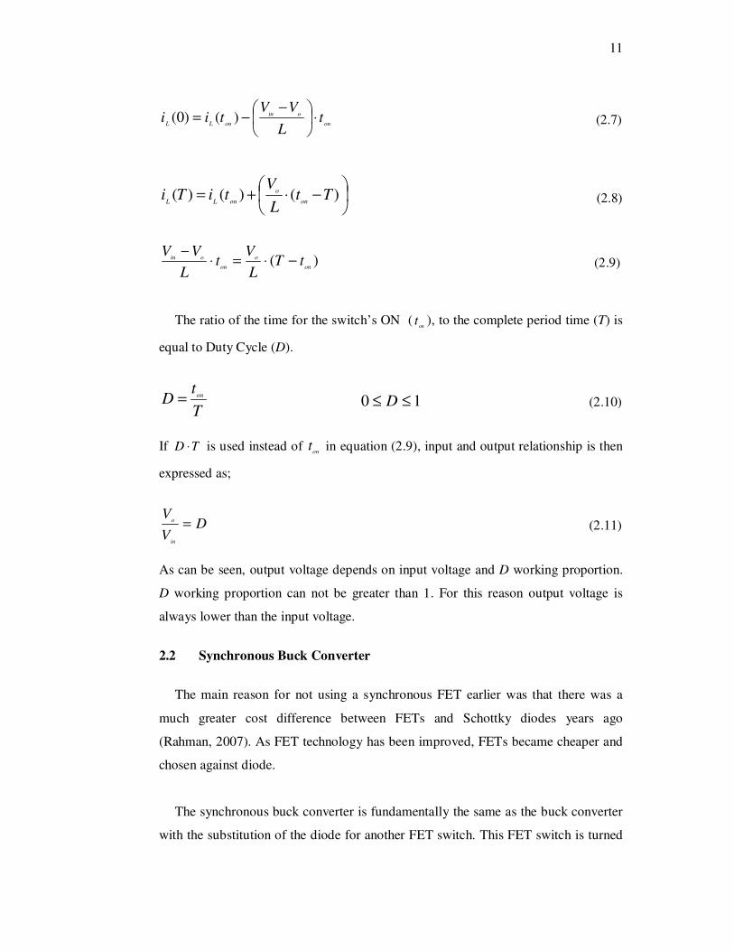
2.1 Non-synchronous Buck Converter ...........................................................8
2.2 Synchronous Buck Converter ................................................................11
2.3 Continuous Current Mode / Discontinuous Current Mode......................14
2.4 Multiphase Buck Converter ...................................................................16
CHAPTER THREE – MULTIPHASE SYNCHRONOUS BUCK
CONVERTER DESIGN CALCULATIONS .....................................................20
3.1 Design Specifications ............................................................................20
3.2 Design Equations...................................................................................22
3.2.1 Number of Phases ..........................................................................22
3.2.2 Duty Cycle.....................................................................................22
3.2.3 Multiphase Controller Selection.....................................................22
3.2.4 Frequency of Operation .................................................................23
vii
3.2.5 Output Inductor Selection ..............................................................23
3.2.6 Output Capacitor Selection ............................................................29
3.2.7 Input Capacitor Selection...............................................................35
3.2.8 MOSFET Selection........................................................................39
3.2.9 Compensation Network Selection ..................................................41
3.2.9.1 Modulator..................................................................................42
3.2.9.2 Output Filter ..............................................................................42
3.2.9.3 The Compensation Network.......................................................44
3.2.9.3.1 Type II (Proportional-Integral) Compensation .....................45
3.2.9.3.2 Type III (Proportional-Integral-Derivative) Compensation. .46
3.3 Summary...............................................................................................54
CHAPTER FOUR – SIMULATION OF MULTIPHASE SYNCHRONOUS
BUCK CONVERTER.........................................................................................56
4.1 Simulation of Two-Phase Synchronous Buck Converter Circuit ............56
4.2 Simulation of Four-Phase Synchronous Buck Converter Circuit ............69
4.3 Summary...............................................................................................79
CHAPTER FIVE – EXPERIMENTAL VERIFICATION ...............................81
5.1 Design of Printed Circuit Board (PCB)..................................................81
5.2 Test Setup..............................................................................................86
5.3 Test Results ...........................................................................................89
5.3.1 Test Results of Designed Two-Phase Synchronous Buck Converter
Circuit............................................................................................89
5.3.1.1 PWM Signals...............................................................................89
5.3.1.2 Output Voltage ............................................................................91
5.3.1.3 Inductor Current Ripple and Sharing............................................92
5.3.1.4 Transient Response....................................................................100
5.3.1.5 Load Regulation - Line Regulation ............................................102
viii
5.3.2 Test Results of Designed Four-Phase Synchronous Buck Converter
Circuit..........................................................................................104
5.3.2.1 PWM Signals.............................................................................104
5.3.2.2 Output Voltage ..........................................................................107
5.3.2.3 Inductor Current Ripple and Sharing..........................................108
5.3.2.4 Transient Response....................................................................116
5.3.2.5 Load Regulation - Line Regulation ............................................118
5.3.3 Efficiency ....................................................................................120
5.3.4 Electromagnetic Compatibility (EMC) Tests................................122
5.3.4.1 CE101 Test (30 Hz – 10 kHz) ....................................................122
5.3.4.2 CE102 Test (10 kHz – 10 MHz) ................................................124
5.3.5 Cost Account ...............................................................................125
5.4 Summary.............................................................................................129
CHAPTER SIX – CONCLUSION ...................................................................131
REFERENCES .................................................................................................134
APPENDIX – A.................................................................................................138
APPENDIX – B.................................................................................................141
APPENDIX – C.................................................................................................143
APPENDIX – D.................................................................................................145

1
CHAPTER ONE
INTRODUCTION
1.1 Introduction
Parallel to the developments in many different fields of technology, energy
converting and as a result, especially DC-DC converters become more and more
important.
With the developments in micro-electronics technology in recent years, it is
necessary to improve the existing DC-DC converters that are used in a variety of
fields as military, aeronautics and astronautics (Terlizzi, 2003). It gets more
important nowadays that especially DC-DC converters with high efficiency, small
dimensions and fast dynamic response are to be used in such systems.
For processes composing a number of systems with a limited power capacity, it is
an essential requirement to design and produce power circuits which supplies high
current values with low voltage.
In addition to the needs in military field, the developments in microprocessors
technology provide low voltage power supplies for microprocessors in computer
systems. As a result of reduction at voltage, the current consumption at
microprocessors increases. Thus, it becomes obligatory to design the power supply of
microprocessors, namely Voltage Regulator Modules (VRMs), with the architecture
of high current, low voltage and capacity of responding to fast load transitions. For
this purpose, to be able to work with high current, operating converters in parallel
became a current issue. On the other hand, to decrease voltage drops, use of
synchronous buck type circuits became widespread (Erdoğan & Aydemir, 2003).
On the other hand, since the dimension and weight are very important for today’s
technological improvements, the new designs must be capable of working at high
frequency values. The dynamic response time of the system to fast load transition
2
gets better by means of extended band interval, obtained by high frequency (Deng,
2005). Multiphase synchronous converter architecture would be used for a more
efficient system, in addition to the improvement in response time by means of high
frequency.
For this purpose, multiphase synchronous buck converter topology, which meets
low voltage and high current requirements of buck type DC/DC converter with high
efficiency by reducing the ripples at output voltage and current, is investigated in this
study.
Based on microprocessor voltage regulator (VR) applications and the voltage
values used in military field most frequently, a two-phase and a four-phase
synchronous buck converters both with 12 V input voltage and an output current 30
A at 3.3V voltage are designed and tested. By the test results, advantages of
multiphase synchronous converters at supplying the power requirements of high-tech
systems are proven.
1.2 Literature Overview
In today’s World, the electricity is a necessity in many fields. The amount of
required electricity varies between milliwatts and megawatts according to the
application field.
Technical properties and the type of electricity in distribution lines differ in
domestic and industrial applications. For these different applications, the flow of the
electricity must be under control and also the type must be converted as required.
These transmission, distribution and control of the electricity are all performed with
power electronics.
“Power electronics refers to control and conversion of electrical power by power
semiconductor devices wherein these devices operate as switches” (Ramaswamy,
n.d.).

3
While realizing the above requirements, Power Electronics aims to decrease the
power loss, increase the efficiency, regulate the output voltage and decrease the
dimensions, weight and total cost of the entire system (Jain & Ayyanar, 2006).
For today’s electronics applications, microprocessors are very important circuit
components and the required power for this essential component is supplied by a
circuitry that is usually called as Voltage Regulator Module (VRM). The preferred
topology for this power converter is the buck converter with synchronous
rectification. The aim of this architecture is providing a lower output voltage to
reduce the ripple both of the output voltage and the input current.
Only six years later than Jack Kilby’s invention of Integrated Circuits (IC) in
1959, Gorden Moore forecasts that the number of transistors doubles for every two
years time (Moore, 1965). This forecast is known as Moore’s law.
By means of the rapid increase at the number of transistors, technical properties
and performance of microprocessors improve much and as a result, required power
for microprocessors also increases.
Processors Intel 386 and Intel 486 use standard 5V supply voltage. Required
voltage of processors is supplied directly from the main power supply. The power of
this main power supply is also used by memory chip, video card and other hardware
parts of a computer.
At the end of the year 1990, voltage lower than 5V supply voltage is started to be
used at Intel Pentium processors. As a result of decrease at the required voltages for
processors, main power supplies become useless. Thus, the first Voltage Regulator
Module is constituted in order to supply power for Pentium I and Pentium II by a
single channel Buck Converter with 5V input voltage (Yao, 2004), (Zhang, 2005).
Ed Stanford (2001), at Intel Power Supply Technology Symposium, declared that
the working voltage for Pentium III has decreased, whereas the current has

4
increased according to power requirements of Pentium II.
It is not an effective solution to use single channel buck converter architecture in
order to generate required power with low voltage and high current, since this
procedure needs equipments with both high costs and larger dimensions in limited
available volumes (Zhou, Wong, Xu, Lee & Huang, 2000).
The multiphase buck topology offers a solution to this conundrum. The
fundamental frequency is effectively multiplied by the number of phases used,
providing high current with small circuit components. Other advantages of this
solution include reduced input and output capacitor RMS currents and reduced EMI
filtering requirements; decreased PCB size; better thermal performance (Saleemi,
2008).
Huy Nguyen (Nguyen, 2004) examined Analysis and Implementation of
Multiphase Synchronous Buck Converter for Transportable Processor to system
designed to improve the efficiency of the voltage regulator converter (VRC) for the
transportable processor in one of his studies in 2004. The four-phase synchronous
buck topology is proposed to provide high efficiency and lower cost solution, which
are the keys in the laptop system.
Current Self Balance Mechanism is proposed for Multiphase Buck Converter by
O. García, P.Zumel, A. de Castro, P. Alou, J.A. Cobos (García, Zumel, Castro, Alou,
& Cobos 2008). For eliminating or at least reducing the unbalance between the
phases, Current Loops are used at “Multiphase Buck Converters” whereas, at
“Digital Controlled and Synchronous Buck Converters” this same purpose is
performed by designing the converters with a phase current ripple higher than twice
the average current value, which is an interesting option. Digital control that reduces
the inequalities of the driving signals of the power MOSFETs and provides high
accuracy in the timing of the driving signals. However, if the current ripple is so high
that there is negative current in the turn-off of the Synchronous MOSFET, the
balance is improved. As a result, to reduce high costs on account of Current Loops, it

5
is convenient to design and produce Multiphase converters in which a high number
of phases are used.
Ekrem Erdoğan (Erdoğan, 2010) investigated Digitally Controlled Multiphase
Synchronous DC-DC Buck Converter Design in a study performed in 2010. The
determination of control parameters providing desired output with analog control
approach and after compose of digital control architecture by use of these
parameters. It is stated that controller architecture is easily convertible by means of
integration of Multiphase Buck Converter and PWM controllers.
In another study by Mohamed A. Shrud, Ahmad H. Kharaz, Ahmed. S. Ashur,
Ahmed Faris and Mustafa Benamar (2010), Analysis and Simulation of Automotive
Interleaved Buck Converter is presented to the importance of multi phase
synchronous buck converter architecture at supplying required power in automotive
industry. By means of this study, the performance of the six phase buck converter
system provides a number of features that do not exist in today's electrical systems.
Furthermore, robustness, good stability, fast dynamic response and equal current
distribution were achieved at the same time the specifications of the automotive
standards were respected.
In this study, first of all, general information about buck circuit topology; non-
synchronous (conventional) buck converter, synchronous buck converter is given.
Then, by investigating Multiphase Synchronous Buck Converter architecture, its
advantages over single phase converters are explained and analyzed.
Lastly, the critical design parameter values are selected using the theoretical
design equations and calculations. Designed circuits are simulated in
Matlab/Simulink to evaluate the performance criteria of the Multiphase Converter.
The prototypes of 100W two-phase and 100W four-phase Multiphase Synchronous
Buck Converter are constructed. The critical performance parameters of the
prototypes are tested and measured.

6
1.3 Aim of This Study
This work is the first effort to introduce multiphase buck converter architecture
for industrial and military applications in which high current, low output voltage and
fast dynamic response are required.
The aim of this study is to determine the superior properties of multiphase buck
converter architecture to existing single-phase buck converter system architecture
and to provide the integration of multiphase buck converter to new systems. Another
important aim of the study is to reduce foreign dependency in Military and
Aerospace Industry by using our own domestic designs for frequently used
Commercial Off – The Shelf (COTS) DC-DC converters.
For this purpose, design of power card is realized with multiphase synchronous
buck converter architecture by mostly taking the required voltage and current values
in military and industrial applications into account.
Different from previous studies:
The test results obtained by increasing the number of phases are realistically
compared. For that purpose, two power cards are designed and produced. Thus,
values of circuit components, efficiency, dynamic response, load – line regulations
and total cost change are realistically examined and compared.
The EMI/EMC effects formed because of high frequency switching are specified
only inscriptively at previous studies. In the scope of this study, CE101 and CE102
tests are performed on the designed power cards according to MIL-STD-461E
military standards. The effects of high frequency switching are observed at the test
results.

7
1.4 Thesis Outline
This thesis is organized in six chapters. Content of the thesis can be summarized
briefly as follows:
Chapter one covers the literature review basics of the single-phase and multiphase
buck converter.
The second chapter introduces non-synchronous and synchronous buck converter
architecture. Continuous and discontinuous current modes related to inductor current
of converter are mentioned. Formulations of inductor current and duty cycle are
given. Furthermore, multiphase buck converter topology is described.
Chapter three is dedicated to multiphase synchronous buck converter design
calculations. Circuit components of designed multiphase buck converters with
different phase number are calculated and selected in order to analyze the advantages
of increasing number of phases in multiphase buck converter topology
In the fourth chapter, simulation results of multiphase synchronous buck
converters are given. Convenience of calculated circuit component values is verified.
Inductor current ripples, output current and voltage ripples are all analyzed and
output current ripple cancellation effect is observed.
In the fifth chapter, inductor current ripples, current sharing between phases,
dynamic response time, load transient response voltage change, line - load
regulations, efficiency and electromagnetic compatibility tests of multiphase
synchronous buck converters with different number of phases are performed and cost
account analysis is obtained.
Finally, chapter six is concerned with conclusions and future works.
8
CHAPTER TWO
ANALYSIS OF BUCK CIRCUIT TOPOLOGY
As in linear power supply, a lower output voltage is provided by buck, or step
down converter. The reason for the choice of the buck power stage by power supply
designers is because the output voltage is always less than the input voltage in the
same polarity and is not isolated from the input (Rogers, 1999).
The main difference between them is that, Buck converters are remarkably
efficient than linear power supplies.
Buck converters are mainly used in regulated dc power supplies, dc motors and
battery powered applications (Mohan, 1995).
Buck circuit can be classified into two groups with respect to low side conducting
device; non-synchronous (conventional) and synchronous buck converter.
2.1 Non-synchronous Buck Converter
A typical non-synchronous buck converter circuit is shown in Figure 2.1. Here,
inV is input voltage,
1Q is switching component,
1D is diode,
1L is inductor, 1
C is
output capacitor and L
R is load resistor.
Figure 2.1 Non-synchronous buck converter topology.
9
Periodic pulses control the 1
Q switch. There are two states, ON state and the OFF
state, in which the circuit given in Figure 2.1 operates.
The two stages of buck converter are shown below.
Figure 2.2 Non-synchronous buck converter, when the switch is ON.
When the switch is ON state, the input provides energy both to the output and to
the inductor (1
L ). During the ON State, the inductor current flows through the switch
and the difference of voltages between inV and o
V is applied to the inductor in the
forward direction (Kamil, 2007).
dt
tdiLVVV L
oinL
)(⋅=−= (2.1)
When the switch 1
Q is conducting, inductor current increases till the end of the
conduction period. This increase is defined as;
dtL
VVtdi
ont ont
oin
L⋅
−=∫ ∫
0 0
)( (2.2)
on
oin
LonLt
L
VViti ⋅
−=− )0()( (2.3)
10
Figure 2.3 Non-synchronous buck converter, when the switch is OFF.
When the switch is at OFF state, the inductor current continues to flow in the
same direction, while the stored energy within the inductor continues to supply the
load current. The inductor current path is completed by the diode 1D during the
1Q
OFF period; thus, it is called a freewheeling diode. During the switch is OFF, the
output voltage oV is applied across the inductor in the reverse direction.
Therefore, Inductor current decreases and maintains current flow till the end of
the OFF period. This decrease is defined as;
∫∫ ⋅−
=T
ont
oin
T
ont
Ldt
L
VVtdi )( (2.4)
)()()(on
o
onLLtT
L
VtiTi −⋅−=− (2.5)
The energy stored in each component is the same at the beginning of one period
and at the end of that period, because of the steady state condition. Inductor current
specifies the stored energy. This causes inductor current to be the same at the
beginning and end of the period;
)()0( TiiLL
= (2.6)
11
on
oin
onLLt
L
VVtii ⋅
−−= )()0( (2.7)
−⋅+= )()()( Tt
L
VtiTi
on
o
onLL (2.8)
)(on
o
on
oin tTL
Vt
L
VV−⋅=⋅
− (2.9)
The ratio of the time for the switch’s ON (on
t ), to the complete period time (T) is
equal to Duty Cycle (D).
T
tD on= 10 ≤≤ D (2.10)
If TD ⋅ is used instead of on
t in equation (2.9), input and output relationship is then
expressed as;
DV
V
in
o = (2.11)
As can be seen, output voltage depends on input voltage and D working proportion.
D working proportion can not be greater than 1. For this reason output voltage is
always lower than the input voltage.
2.2 Synchronous Buck Converter
The main reason for not using a synchronous FET earlier was that there was a
much greater cost difference between FETs and Schottky diodes years ago
(Rahman, 2007). As FET technology has been improved, FETs became cheaper and
chosen against diode.
The synchronous buck converter is fundamentally the same as the buck converter
with the substitution of the diode for another FET switch. This FET switch is turned
12
on and off synchronously with the buck MOSFET. Therefore, this topology is known
as the synchronous buck converter.
In designs that require high current and low output voltage, the excessive power
loss inside the freewheeling diode, limits the minimum output voltage that can be
achieved. To reduce the loss at high current and to achieve lower output voltage, the
freewheeling diode is replaced by a MOSFET with a very low ON state resistance
)(ONDSR (Kamil, 2007).
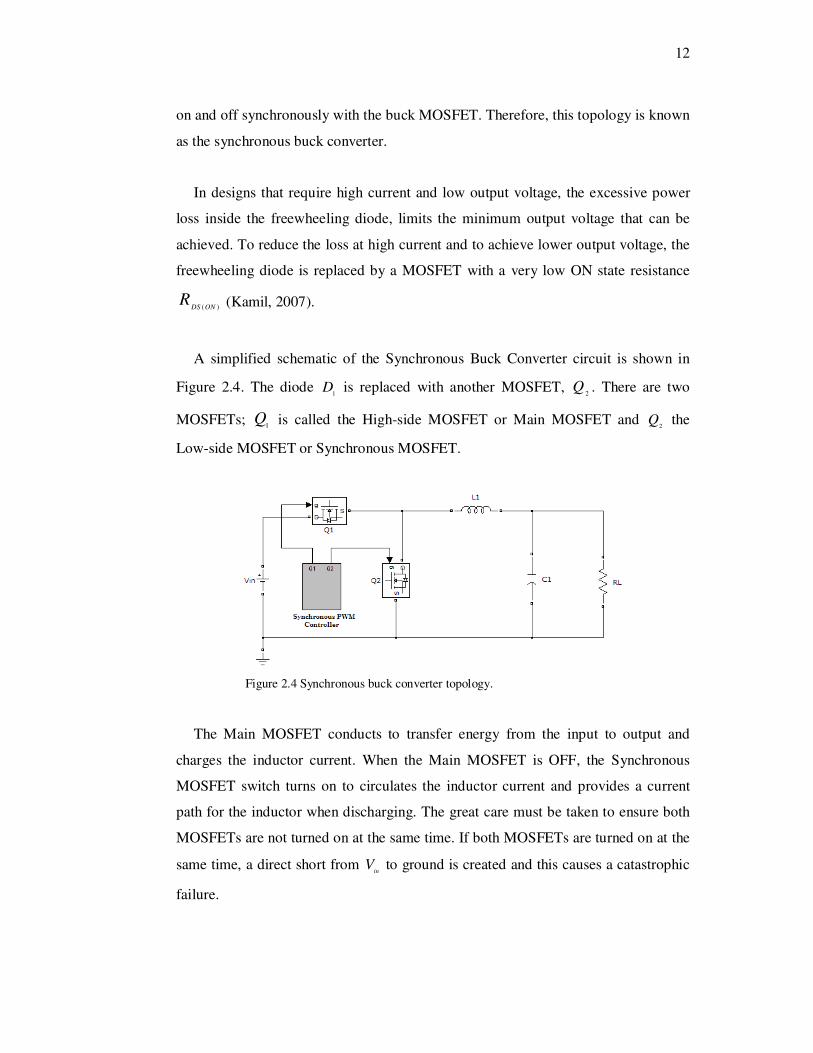
A simplified schematic of the Synchronous Buck Converter circuit is shown in
Figure 2.4. The diode 1
D is replaced with another MOSFET, 2
Q . There are two
MOSFETs; 1Q is called the High-side MOSFET or Main MOSFET and
2Q the
Low-side MOSFET or Synchronous MOSFET.
Figure 2.4 Synchronous buck converter topology.
The Main MOSFET conducts to transfer energy from the input to output and
charges the inductor current. When the Main MOSFET is OFF, the Synchronous
MOSFET switch turns on to circulates the inductor current and provides a current
path for the inductor when discharging. The great care must be taken to ensure both
MOSFETs are not turned on at the same time. If both MOSFETs are turned on at the
same time, a direct short from in
V to ground is created and this causes a catastrophic
failure.
13
The resultant voltage drop across the MOSFET can be smaller than the forward
voltage drop of the freewheeling diode. Also, lower resistance from Drain to Source
()(ONDS
R ) helps to reduce losses substantially and therefore optimizes the overall
conversion efficiency of the synchronous MOSFET.
To show that Synchronous Buck Converter reduces losses substantially and
accordingly increases the efficiency greatly, equations are given below. First,
consider the case when there is a diode. The equation for power loss across a diode
can be calculated by equation (2.12).
( )DIVPODD
−⋅⋅= 1max (2.12)
Assume that the input is 12V, the output is 3.3 V and the load current is 30A. In
this case the duty cycle will be 27.5% and the diode will be ON for 72.5% of the
time. A typical Schottky diode (B340LB) with a 0.4V would suffer from a power
loss of 8.7 W. The power loss for the synchronous regulator at 30A;
( )DRIPONDSOS
−⋅⋅= 1)(
2
max (2.13)
A typical MOSFET (FDS6699S) with a 3.6 mΩ (
)(ONDSR ) would suffer a power
loss of 2.349 W.
It can be seen that the power loss mainly depends upon the duty cycle. A
synchronous buck converter generally has lower losses than a Schottky diode, and as
a result its use is quite popular in low voltage DC/DC converters.
Synchronous buck converters are attracted attention for low-voltage power
conversion because of its high efficiency and reduced area consumption (Mulligan,
Broach, and Lee, 2005).
14
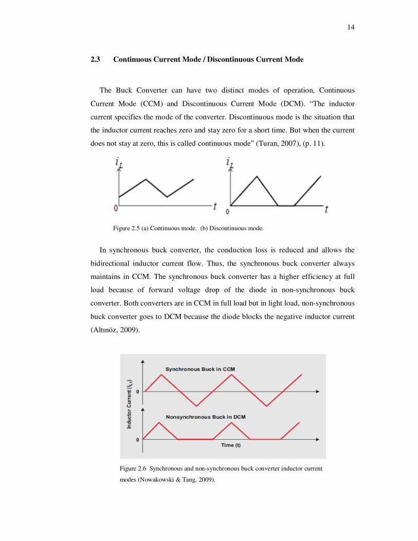
2.3 Continuous Current Mode / Discontinuous Current Mode
The Buck Converter can have two distinct modes of operation, Continuous
Current Mode (CCM) and Discontinuous Current Mode (DCM). “The inductor
current specifies the mode of the converter. Discontinuous mode is the situation that
the inductor current reaches zero and stay zero for a short time. But when the current
does not stay at zero, this is called continuous mode” (Turan, 2007), (p. 11).
Figure 2.5 (a) Continuous mode. (b) Discontinuous mode.
In synchronous buck converter, the conduction loss is reduced and allows the
bidirectional inductor current flow. Thus, the synchronous buck converter always
maintains in CCM. The synchronous buck converter has a higher efficiency at full
load because of forward voltage drop of the diode in non-synchronous buck
converter. Both converters are in CCM in full load but in light load, non-synchronous
buck converter goes to DCM because the diode blocks the negative inductor current
(Altınöz, 2009).
Figure 2.6 Synchronous and non-synchronous buck converter inductor current
modes (Nowakowski & Tang, 2009).
15
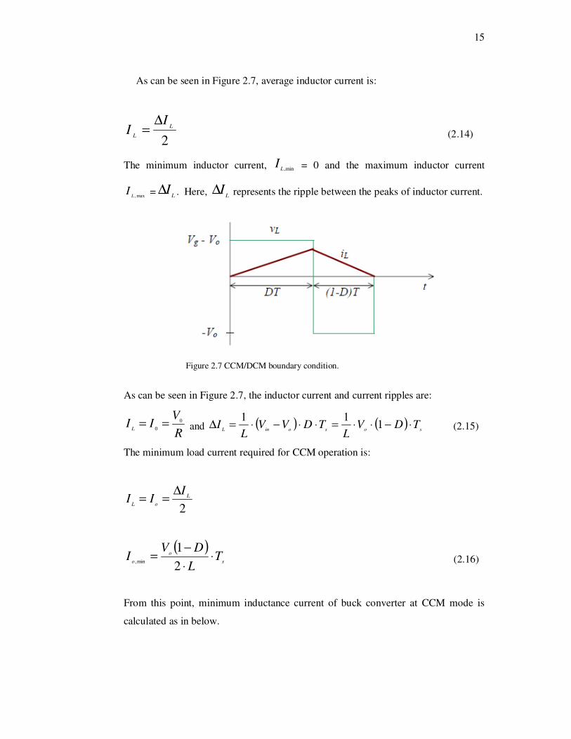
As can be seen in Figure 2.7, average inductor current is:
2L
L
II
∆= (2.14)
The minimum inductor current, min,LI
= 0 and the maximum inductor current
max,LI = L
I∆ . Here, LI∆ represents the ripple between the peaks of inductor current.
Figure 2.7 CCM/DCM boundary condition.
As can be seen in Figure 2.7, the inductor current and current ripples are:
R
VII
L
0
0== and ( ) ( )
sosoinLTDV
LTDVV
LI ⋅−⋅⋅=⋅⋅−⋅=∆ 1
11 (2.15)
The minimum load current required for CCM operation is:
2L
oL
III
∆==
( )s
o
oT
L
DVI ⋅
⋅
−=
2
1min, (2.16)
From this point, minimum inductance current of buck converter at CCM mode is
calculated as in below.
16
( )
so
o
fI
DVL
⋅⋅
−⋅⟩
min,2
1 (2.17)
According to the equation (2.17), in order to provide the CCM mode and to reduce
the inductance value, switching frequency must be increased.
2.4 Multiphase Buck Converter
The buck converter should be capable of transferring energy from the input to the
output quickly during the transient response periods. This is performed by small
inductances. But, small inductances, by resulting in large current ripples in the
converter, increase the steady-state voltage ripples at the output capacitors. For
improving the transient responses, the inductances need to be so small that the
steady-state voltage ripples could be comparable to transient voltage spikes.
Converter’s working in such conditions is impractical (Wong, 2001).
To reduce the total current ripples flowing into the output capacitors and optimize
the input and output capacitor all the parallel converters operate on the same time
base and each converter starts switching after a fixed time/phase from the previous
one. This type of converter is called a multiphase synchronous buck converter
(Kamil, 2007). The fixed time/phase is given by Time period/n or 360/n, where “n”
is the number of the converter connected in parallel. The steady-state voltage ripples
at the output capacitors are mostly reduced with the current ripple reduction. The
transient voltage spikes can also be reduced due to the smaller output inductances.
The requirements of both the transient voltage spikes and the steady-state output
voltage ripples can be met by a much smaller output capacitance (Wong, 2001).
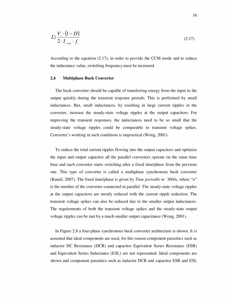
In Figure 2.8 a four-phase synchronous buck converter architecture is shown. It is
assumed that ideal components are used, for this reason component parasitics such as
inductor DC Resistance (DCR) and capacitor Equivalent Series Resistance (ESR)
and Equivalent Series Inductance (ESL) are not represented. Ideal components are
shown and component parasitics such as inductor DCR and capacitor ESR and ESL
17
are not represented. In case of four phases synchronous buck converter, control
signal for each phase is shifted from each other by (360/n) 90° degrees.
Figure 2.8 Four-phase synchronous buck converter.
18
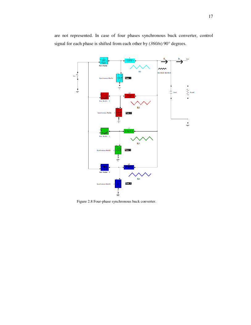
Figure 2.9 Main waveforms of four-phase synchronous buck converter in steady state conditions.
The multiphase buck converter has endogenous advantages over its single-phase
counterpart and is a proper candidate in many applications, given the trend towards
lower supply voltages and greater load-current requirements. Multiphase buck
converter is generally found in VRMs for computing and server applications where
high output current and fast transient response is crucial (Hegarty, 2007).
The essential limitation of the conventional single-phase buck converter is the
trade-off of efficiency and switching frequency. Output ripple and dynamic response
are improved by increased switching frequency. The physical size and value of the
filter inductor and capacitors get smaller at higher switching frequencies. However,
there is a practical limitation to the switching frequency, switching losses increase
with frequency, and as a result efficiency tends to be lower. The multiphase buck
converter architecture proposes a solution to this conundrum. When the fundamental
frequency is multiplied by the number of phases used, it improves transient response
(Hegarty, 2007).

19
The main benefit of multiphase synchronous buck converter is the current ripple
cancellation effect which enables the use of the small inductance to both improve
transient response, minimize the output capacitance, lower cost of output capacitors,
few components and reduced the power dissipation (Saleemi, 2008).
Figure 2.9 shows an example of four-phase ripple cancellation of inductor current.
The total ripple of inductor current ( )4321 LLLL
IIII +++ has smaller magnitude and
four times ripple frequency than individual channel or phase.
Multiphase synchronous buck converter combines all phase shifted inductor
currents from individual channel or phase, and therefore greatly reduces the total
current ripple flowing into the output capacitor (Saleemi, 2008).
Another benefit of multiphase synchronous buck converter is with the current
ripple reduction, the output voltage ripples are also greatly reduced which enables the
use of very small inductances in each phase to improve the transient response
requirement (Saleemi, 2008).
The multiphase buck converter increases the total inductor current (output current)
ripple frequency. The output current ripple frequency of multiphase buck converter is
obtained by the multiply of switching frequency of each buck converter and the
number of parallel converters (Kamil, 2007).
PHPHRPLfNF ⋅= (2.18)
This provides another advantage of multiphase because the higher the output
current ripple frequency the less filtering effort needed. Moreover, it reduces the
amount of output capacitance (Saleemi, 2008).
Consequently, multiphase buck converter architecture helps to improve the load
transient performance, to minimize the input and output capacitance, to reduce EMI
filtering requirements, to decrease of circuit components dimensions and accordingly
of PCB dimensions.
20
CHAPTER THREE
MULTIPHASE SYNCHRONOUS BUCK CONVERTER DESIGN CALCULATIONS
Before implementing multiphase synchronous buck converter design, it is
important to know which parameters are of the utmost concern. The various concerns
could be the optimization for circuit performance, component cost, and efficiency.
Multiphase synchronous buck converter design is introduced in two sections. First
part includes specifications in design of two-phase and four-phase synchronous buck
converter circuits. Second part is dedicated to calculating circuit components of two-
phase and four-phase synchronous buck converters.
3.1 Design Specifications
The design of the power circuits are made according to the specifications in Table
3.1 and Table 3.2.
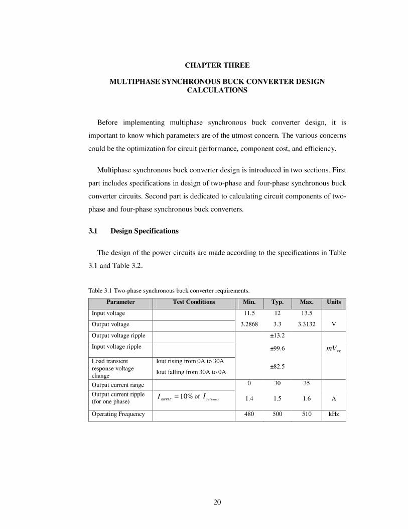
Table 3.1 Two-phase synchronous buck converter requirements.
Parameter Test Conditions Min. Typ. Max. Units
Input voltage 11.5 12 13.5
Output voltage 3.2868 3.3 3.3132 V
Output voltage ripple ±13.2
Input voltage ripple ±99.6 PK
mV
Load transient response voltage change
Iout rising from 0A to 30A
Iout falling from 30A to 0A ±82.5
Output current range 0 30 35
Output current ripple (for one phase)
%10=RIPPLE
I of (max)PH
I
1.4 1.5 1.6 A
Operating Frequency 480 500 510 kHz
21
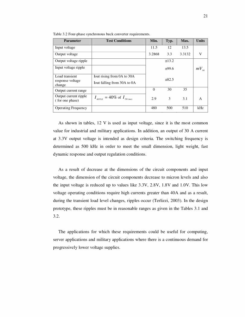
Table 3.2 Four-phase synchronous buck converter requirements.
Parameter Test Conditions Min. Typ. Max. Units
Input voltage 11.5 12 13.5
Output voltage 3.2868 3.3 3.3132 V
Output voltage ripple ±13.2
Input voltage ripple ±99.6 PK
mV
Load transient response voltage change
Iout rising from 0A to 30A
Iout falling from 30A to 0A ±82.5
Output current range 0 30 35
Output current ripple ( for one phase)
%40=RIPPLE
I of (max)PH
I
2.9 3 3.1 A
Operating Frequency 480 500 510 kHz
As shown in tables, 12 V is used as input voltage, since it is the most common
value for industrial and military applications. In addition, an output of 30 A current
at 3.3V output voltage is intended as design criteria. The switching frequency is
determined as 500 kHz in order to meet the small dimension, light weight, fast
dynamic response and output regulation conditions.
As a result of decrease at the dimensions of the circuit components and input
voltage, the dimension of the circuit components decrease to micron levels and also
the input voltage is reduced up to values like 3.3V, 2.8V, 1.8V and 1.0V. This low
voltage operating conditions require high currents greater than 40A and as a result,
during the transient load level changes, ripples occur (Terlizzi, 2003). In the design
prototype, these ripples must be in reasonable ranges as given in the Tables 3.1 and
3.2.
The applications for which these requirements could be useful for computing,
server applications and military applications where there is a continuous demand for
progressively lower voltage supplies.

22
3.2 Design Equations
After electrical specifications, in this part, according to needs including capacitor,
inductor, MOSFETs, drivers and controllers, different components of converter will
be calculated.
3.2.1 Number of Phases
In this study, both of these two converters were designed by using the multiphase
synchronous buck converter architecture. One of these converters is two-phase, the
other one is four-phase.
Since the switching frequency is 500 kHz, the two-phase will provide the output
frequency of 1 MHz and four-phase will provide the output frequency of 2 MHz due
to the frequency multiplication effect (equation 2.18).
3.2.2 Duty Cycle
Duty cycle for the overall converter can be calculated as below:
275.012
3.3===
V
V
V
VD
in
o
3.2.3 Multiphase Controller Selection
In the two-phase and four-phase synchronous buck converter designs, the Texas
Instruments TPS40090 PW high frequency, multiphase controller was used.
The TPS40090 PW provides fixed frequency, peak current mode control with
forced phase current balancing. Phase currents are sensed by using direct current
resistance (DCR) of inductors. Other features include a single voltage operation, a
true differential output voltage sense amplifier, a user programmable current limit,
soft start and a power good indicator (Texas Instruments TPS40090 Datasheet,
2006).

23
3.2.4 Frequency of Operation
The clock frequency for the TPS40090 PW controller is programmed with a
single resistor from the RT pin to ground. Equation (3.1) from the data sheet allows
selection of the RT resistor in Ωk for a given switching frequency in kHz as shown
below (Texas Instruments TPS40090 Datasheet, 2006):
)7102.39( 041.13 −×××= −
PHPHRTfKR (3.1)
where,
PHK is a coefficient that depends on the number of active phases for two-phase and
three-phase configurations PH
K = 1.333 and for four-phase PH
K =1 is a single phase
frequency, kHz.
PHf is the single phase frequency (in kHz).
For 500 kHz switching frequency, RT resistor is calculated to be 71.66 Ωk for
two-phase converter and 53.76 Ωk is calculated for four-phase converter. The
resistors with 53.6 Ωk and 71.5 Ωk standard values are used instead of 53.76 Ωk
and 71.66 Ωk .
3.2.5 Output Inductor Selection
The most important circuit parameter providing desired and required circuit
function is Inductance. Additionally, it is generally the first and main parameter to be
calculated. by calculating this value, both certain amount of energy storage is
provided and output current ripple is reduced.
The ripple at the inductor current is not a desired situation. It must be limited. The
ripple performs an important role at the value of inductance. The relation between
the value and current ripple of inductance is given equations (3.2), (3.3) and (3.4)
(Mohan, 1995).
)()(1
)( tdtvL
tiLL ∫ ⋅= (3.2)

24
As can be understood from the equation (3.2), the ripple at inductance current is
determined by the proportion of the area under the inductance voltage in Figure 3.1
to inductance value.
Output inductor design equation can be developed from Figure 3.1 the inductor
ripple current at on and off time.
Inductor current rises: S
oin
PHLTD
L
VVI ⋅⋅
−=∆
, (3.3)
Inductor current decreases: S
o
PHLTD
L
VI ⋅−⋅=∆ )1(
, (3.4)
Here, inV is input voltage, o
V is output voltage, D is duty cycle, S
T is switching
period and L is output inductor.
According to volt-second balance at inductance, the average voltage on the
inductance must be zero. Accordingly, the area stated as A and B in Figure 3.1 must
be equal. From this:
s
o
s
oin
PHLTD
L
VTD
L
VVI ⋅−⋅=⋅⋅
−=∆ )1(
, (3.5)
is obtained. From the equation (3.5), the equation (3.6) is obtained for the value of output
inductance.
PHL
SO
I
TDVL
,
)1(
∆
⋅−⋅= or
SPHL
O
fI
DVL
⋅∆
−⋅=
,
)1( (3.6)
25
Figure 3.1 The main waveforms of the voltages and currents
for a synchronous buck converter (Erdoğan, 2010).
The relation between the value of multiphase buck converter’s inductance and
efficiency is given in Figure 3.2. As can be seen in this figure, efficiency of the
multiphase buck converter increases with increasing inductance value. This situation
is obtained by decrease at current ripples which is a result of increase at inductance
value. By means of that, both conduction and switching losses decrease (Dong,
2009).
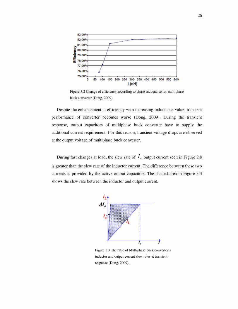
26
Figure 3.2 Change of efficiency according to phase inductance for multiphase
buck converter (Dong, 2009).
Despite the enhancement at efficiency with increasing inductance value, transient
performance of converter becomes worse (Dong, 2009). During the transient
response, output capacitors of multiphase buck converter have to supply the
additional current requirement. For this reason, transient voltage drops are observed
at the output voltage of multiphase buck converter.
During fast changes at load, the slew rate of 0I output current seen in Figure 2.8
is greater than the slew rate of the inductor current. The difference between these two
currents is provided by the active output capacitors. The shaded area in Figure 3.3
shows the slew rate between the inductor and output current.
Figure 3.3 The ratio of Multiphase buck converter’s
inductor and output current slew rates at transient
response (Dong, 2009).
27
The shaded part in Figure 3.3 is determined by the inductor current slew rate and
the magnitude of the current step. Determination of the current step magnitude is
made by the unalterable applications. The only way to reduce the shaded part is to
increase the current slew rate flowing into the multiphase buck converter output
capacitors so that the transient voltage spike on the capacitors can be reduced (Wong,
2001).
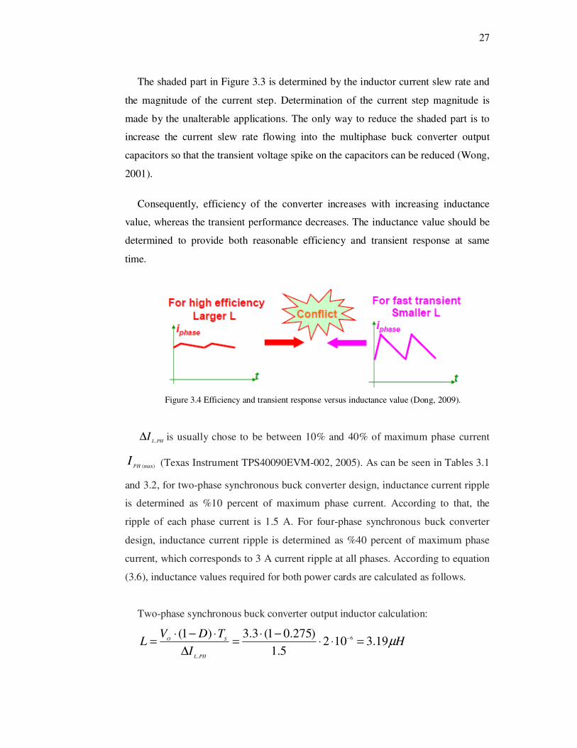
Consequently, efficiency of the converter increases with increasing inductance
value, whereas the transient performance decreases. The inductance value should be
determined to provide both reasonable efficiency and transient response at same
time.
Figure 3.4 Efficiency and transient response versus inductance value (Dong, 2009).
PHLI
,∆ is usually chose to be between 10% and 40% of maximum phase current
(max)PHI (Texas Instrument TPS40090EVM-002, 2005). As can be seen in Tables 3.1
and 3.2, for two-phase synchronous buck converter design, inductance current ripple
is determined as %10 percent of maximum phase current. According to that, the
ripple of each phase current is 1.5 A. For four-phase synchronous buck converter
design, inductance current ripple is determined as %40 percent of maximum phase
current, which corresponds to 3 A current ripple at all phases. According to equation
(3.6), inductance values required for both power cards are calculated as follows.
Two-phase synchronous buck converter output inductor calculation:
HI
TDVL
PHL
SO µ19.31025.1
)275.01(3.3)1( 6
,
=⋅⋅−⋅
=∆
⋅−⋅= −
28
Four-phase synchronous buck converter output inductor calculation:
HI
TDVL
PHL
SO µ59.11023
)275.01(3.3)1( 6
,
=⋅⋅−⋅
=∆
⋅−⋅= −
Since the power circuits work in continuous current mode, according to equation
(2.17), the minimum inductance value for two-phase synchronous buck converter is;
( )H
fI
DVL
so
o µ478.01050052
)275.01(3.3
2
13
min,
=×××
−×=
⋅⋅
−⋅⟩
To insure working at continuous current mode, the minimum inductance value for
four-phase synchronous buck converter is;
( )H
fI
DVL
so
o µ957.010500)4/5(2
)275.01(3.3
2
13
min,
=×××
−×=
⋅⋅
−⋅⟩
Minimum inductance values calculated for two-phase and four-phase synchronous
buck converters are greater than the value that is required to work in Continuous
Current Mode. Thus, both power cards work in Continuous Current Mode.
Another important issue while determining the calculated inductance value is the
maximum exposed current and working frequency. These criteria’s prevent
inductances from over-heating in operation.
For two-phase synchronous buck converter circuitry, inductance SER2915L-
332KL produced by Coilcraft is used because of its physical dimension and low DC
resistance. Inductance value is 3.3 Hµ and DCR value is 1.50 Ωm .
For four-phase synchronous buck converter circuitry, inductance MVR1271C-
162ML produced by Coilcraft is used because of its physical dimension and low DC
resistance. Inductance value is 1.65 Hµ and DCR value is 2.53 Ωm .
29
3.2.6 Output Capacitor Selection
In Switch Mode Power Supply, output capacitance stores energy in its electric
field resulted by the voltage applied. Thus, qualitatively, the function of the capacitor
is to hold the output voltage constant.
The value of output capacitance of buck converter power stage is generally
selected to limit output voltage ripple to the level required by the specification.
Determination of the output voltage ripple is primarily done by the series impedance
of the capacitor, because the determination of the ripple current in the output
inductor is generally already done (Rogers, 1999).
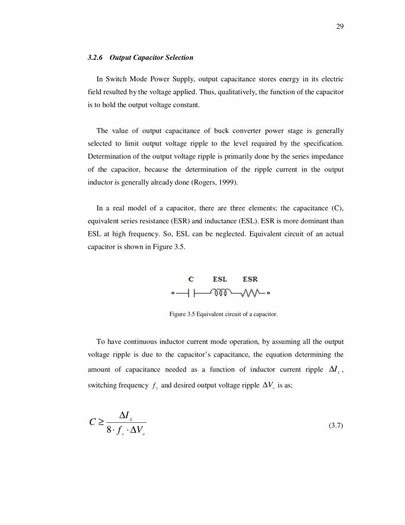
In a real model of a capacitor, there are three elements; the capacitance (C),
equivalent series resistance (ESR) and inductance (ESL). ESR is more dominant than
ESL at high frequency. So, ESL can be neglected. Equivalent circuit of an actual
capacitor is shown in Figure 3.5.
Figure 3.5 Equivalent circuit of a capacitor.
To have continuous inductor current mode operation, by assuming all the output
voltage ripple is due to the capacitor’s capacitance, the equation determining the
amount of capacitance needed as a function of inductor current ripple L
I∆ ,
switching frequency S
f and desired output voltage ripple o
V∆ is as;
os
L
Vf
IC
∆⋅⋅
∆≥
8 (3.7)
30
The peak to peak value of total output ripple current to be filtered by the output
capacitor can be as expressed by equation (3.8) (Hegarty, 2007; Saleemi, 2008).
( )DNmDN
m
fL
VIi
s
o
Lpkpkcout⋅−+⋅
⋅
−⋅
=∆=−
11, (3.8)
RCMNORMLRIPPLEKKII ⋅=∆= (3.9)
where s
o
NORM
fL
VK
⋅= , ( )DNm
DN
mK
RCM⋅−+⋅
⋅
−= 11 is output ripple
current cancellation multiplier, N is the number of the converter connected in
parallel, D is duty cycle, L is inductor of each phase defined in equation (3.6),
)( DNfloorm ⋅= and the floor function returns the greatest integer value less than
the argument (Saleemi, 2008).
Output Ripple Current Cancellation Multiplier, RCM
K value, given in equation
(3.9) can be found by using duty cycle value with the graphic given in Figure 3.6
(TPS40090EVM-002, User’s Guide, Texas Instruments).
31
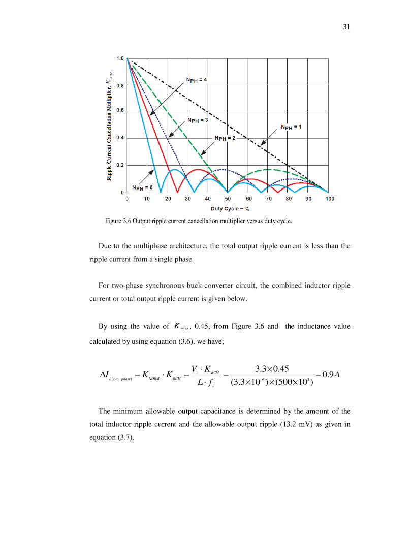
Figure 3.6 Output ripple current cancellation multiplier versus duty cycle.
Due to the multiphase architecture, the total output ripple current is less than the
ripple current from a single phase.
For two-phase synchronous buck converter circuit, the combined inductor ripple
current or total output ripple current is given below.
By using the value of RCM
K , 0.45, from Figure 3.6 and the inductance value
calculated by using equation (3.6), we have;
AfL
KVKKI
s
RCMo
RCMNORMphasetwoL9.0
)10500()103.3(
45.03.336)(
=×××
×=
⋅
⋅=⋅=∆
−−
The minimum allowable output capacitance is determined by the amount of the
total inductor ripple current and the allowable output ripple (13.2 mV) as given in
equation (3.7).

32
FFVf
IC
os
L µ04.1710704.1)102.13()10500(8
9.0
85
33=×=
××××=
∆⋅⋅
∆≥ −
−
For four-phase synchronous buck converter circuit, the combined inductor ripple
current or total output ripple current is given below.
By using the value of RCM
K , 0.082, from Figure 3.6 and the inductance value
calculated by using equation (3.6), we have;
AfL
KVKKI
s
RCMo
RCMNORMphasefourL328.0
)10500()1065.1(
082.03.336)(
=×××
×=
⋅
⋅=⋅=∆
−−
and the minimum allowable output capacitance is:
FFVf
IC
os
L µ21.61021.6)102.13()10500(8
328.0
86
33=×=
××××=
∆⋅⋅
∆≥ −
−
The most important issue while determining the output capacitance value is the
limitation of transient voltage ripples resulted by fast current changes to design
target. The calculations of transient voltage ripple due to fast increasing and
decreasing of output current are calculated as in the equations (3.10) and (3.11)
(Lynch & Hesse, 2006).
( )oinMAX
STEPEQ
under
VVDC
ILV
−⋅⋅⋅
⋅=
2
2
(3.10)
out
STEPEQ
over
VC
ILV
⋅⋅
⋅=
2
2
(3.11)

33
Where, EQ
L is equivalent inductance value (for two-phase L/2 and four-phase L/4),
STEPI is output current step value, C is the output capacitance value,
MAXD is the
maximum duty cycle, in
V is input voltage and out
V is output voltage.
MAXD , found according to the datasheet TPS40090 of Texas Instruments, is 83.3%
for two - three phase and 87.5% for four phase applications.
As can be seen from the design requirements given in Tables 3.1 and 3.2,
maximum transient voltage ripple at output voltage of power cards due to 30 A
change of current is 2.5%, corresponding to 82.5 mV.
Below are the calculations of two and four phase capacitance values respectively,
limiting the ripple to 82.5mV for an increase of 30A at output current.
For two-phase synchronous buck converter circuit:
( ) ( )FF
VVDV
ILC
oinMAXunder
STEPEQ
µ124110241.13.312833.0105.822
30)2103.3(
2"3
3
262
=×=−××××
××=
−⋅⋅⋅
⋅≥
−
−
−
For four-phase synchronous buck converter circuit:
( ) ( )FF
VVDV
ILC
oinMAXunder
STEPEQ
µ2951095.23.312875.0105.822
30)41065.1(
2"4
3
262
=×=−××××
××=
−⋅⋅⋅
⋅≥ −
−
−
Similarly, calculations for a decrease of 30A at output current are;
For two-phase synchronous buck converter circuit:
FFVV
ILC
outover
STEPEQ
µ272710727.23.3105.822
30)2103.3(
23
3
262
=×=×××
××=
⋅⋅
⋅≥ −
−
−
For four-phase synchronous buck converter circuit:
FFVV
ILC
outover
STEPEQ µ6811081.63.3105.822
30)41065.1(
24
3
262
=×=×××
××=
⋅⋅
⋅≥ −
−
−
34
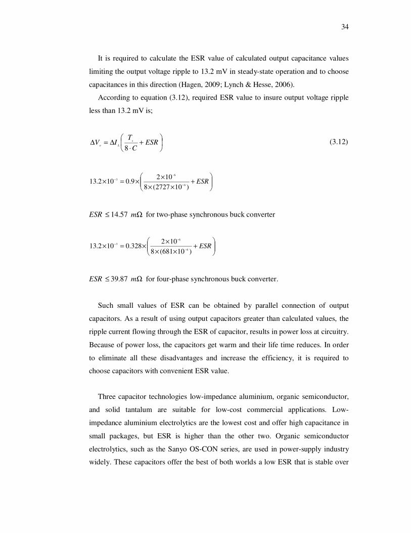
It is required to calculate the ESR value of calculated output capacitance values
limiting the output voltage ripple to 13.2 mV in steady-state operation and to choose
capacitances in this direction (Hagen, 2009; Lynch & Hesse, 2006).
According to equation (3.12), required ESR value to insure output voltage ripple
less than 13.2 mV is;
+
⋅∆=∆ ESR
C
TIV s
Lo
8 (3.12)
+
××
××=×
−
−
− ESR)102727(8
1029.0102.13
6
6
3
ESR ≤ 14.57 Ωm for two-phase synchronous buck converter
+
××
××=×
−
−
−ESR
)10681(8
102328.0102.13
6
6
3
ESR ≤ 39.87 Ωm for four-phase synchronous buck converter.
Such small values of ESR can be obtained by parallel connection of output
capacitors. As a result of using output capacitors greater than calculated values, the
ripple current flowing through the ESR of capacitor, results in power loss at circuitry.
Because of power loss, the capacitors get warm and their life time reduces. In order
to eliminate all these disadvantages and increase the efficiency, it is required to
choose capacitors with convenient ESR value.
Three capacitor technologies low-impedance aluminium, organic semiconductor,
and solid tantalum are suitable for low-cost commercial applications. Low-
impedance aluminium electrolytics are the lowest cost and offer high capacitance in
small packages, but ESR is higher than the other two. Organic semiconductor
electrolytics, such as the Sanyo OS-CON series, are used in power-supply industry
widely. These capacitors offer the best of both worlds a low ESR that is stable over
35
the temperature range and high capacitance in a small package. Most of the OS-CON
units are supplied in lead-mounted radial packages; surface-mount devices are
available but much of the size and performance advantage is sacrificed. Solid-
tantalum chip capacitors are probably the best choice if a surface-mounted device is
an absolute must. Products such as the AVX TPS family and the Sprague 593D
family were developed for power-supply applications. These products offer a low
ESR that is relatively stable over the temperature range, high ripple-current
capability, low ESL, surge-current testing, and a high ratio of capacitance to volume
(Rogers, 1999).
Eventually, eight TPS type, surface mount solid electrolyte, 330 Fµ with 45 Ωm
ESR capacitors produced by AVX company and against the high frequency
parasitics, four surface mount ceramic, 22 Fµ with 2 Ωm ESR capacitors produced
by TDK are used. The ESR value is reduced by parallel connection of the capacitors.
ESR value is calculated approximately 0.46 Ωm , which is convenient and less than
previously calculated ESR value.
For four phase converter, six TPS type, surface mount solid electrolyte, 150 Fµ
with 50 Ωm ESR capacitors produced by AVX company and against the high
frequency parasitics, five surface mount ceramic, 22 Fµ with 2 Ωm ESR capacitors
produced by TDK are used. The ESR value is reduced by parallel connection of the
capacitors. ESR value is calculated approximately 0.4 Ωm which is convenient and
less than previously calculated ESR value.
3.2.7 Input Capacitor Selection
In the multiphase buck converter, the input capacitor provides a low-impedance
voltage source for the converter and helps to filter the ripple current.
The multiphase buck converter input ripple RMS current is expressed by equation
(3.13) (Hegarty, 2007; TPS40090EVM-002, User’s Guide, Texas Instruments).
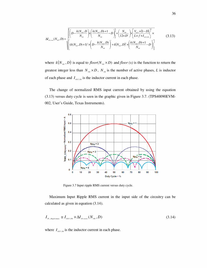
36
(3.13)
where ( )DNkPH
, is equal to )( DNfloorPH
× and floor (x) is the function to return the
greatest integer less than DNPH
× , PH
N is the number of active phases, L is inductor
of each phase and PHOUT
I,
is the inductor current in each phase.
The change of normalized RMS input current obtained by using the equation
(3.13) versus duty cycle is seen in the graphic given in Figure 3.7. (TPS40090EVM-
002, User’s Guide, Texas Instruments).
Figure 3.7 Input ripple RMS current versus duty cycle.
Maximum Input Ripple RMS current in the input side of the circuitry can be
calculated as given in equation (3.14).
),()(,(max)_
DNIIIPHnomINPHOUTRippleIN
∆×≅ (3.14)
where
PHOUTI
,is the inductor current in each phase.
( )
( )
−
+×+
−×+
×
××
−××
×
+
−
+×
−
=∆3
2
3
2
2
,
2
)(
1),(,
),()1),((
1
12
1),(,(
),(
DN
DNkDNk
N
DNkDDNk
IfL
DV
D
ND
N
DNk
N
DNkD
DNI
PH
PH
PH
PH
PH
PH
PHOUT
OUTPH
PH
PH
PH
PH
PHnomIN

37
The value of input capacitance of converter power stage is generally selected to
limit input voltage ripple to the level required by the specification. The minimum
input capacitance can be calculated from equation (3.17).
dt
dVCi in
C= (3.15)
Equation (3.15) can be written as
in
C
dV
dtiC = (3.16)
where
Ci is equal to
(max)_ RippleINI (equation 3.14), therefore
in
SPHnomINPHOUT
in
SRippleIN
IN
V
TDDNII
V
TDIC
∆
××∆×=
∆
××=
),()(,(max)_ (3.17)
According to equation (3.13), the input ripple current of two-phase synchronous
buck converter is;
ADIphasetwoIN
25.0),2(__
=∆
Input ripple current, 0.25 A, obtained by the calculation is same as the value that
correspond to 27.5% duty cycle given in Figure 3.7. Consequently, instead of making
long calculations, it is possible to determine a close value for input ripple current by
means of this graphic.
Maximum possible input ripple RMS current value at input side of the circuitry is
calculated by using the equation (3.14).
( )
( )
−
+×+
−×+
×
××××
−××
×
+
−
+×
−
=∆
−
3
2
3
2
2
362
__
275.02
100
2
0275.0)10(
1510500103.3
275.013.3
275.012
2275.0
2
10
2
0275.0
),2( DIPhaseTwoIN
38
AIRippleIN
75.325.015(max)_
=×≅
According to the calculations above, for full load case, maximum current ripple at
input side of two-phase synchronous buck converter circuit is found as 3.75 A. This
input current ripple and minimum input capacitor value that limits the input voltage
ripple to required 0.83% value, corresponding 99.6 mV are calculated by using the
equation (3.17).
FV
TDIC
in
SRippleIN
INµ7.20
106.99
102275.075.33
6
(max)_=
×
×××=
∆
××=
−
−
For a typical ripple voltage of 99.6 mV the maximum ESR is calculated:
Ω==×
=∆
∆=
−
mI
VESR
IN
in 5.260265.075.3
106.99 3
For two-phase synchronous buck converter, two SVP type, surface mount
aluminium electrolyte, 100 µF with 24 mΩ ESR capacitors produced by Sanyo
company are used. Additionally, to eliminate the input current spikes, a Nichicon
type, 220 µF capacitor is connected in parallel with other two capacitors. Final ESR
value of these parallel connected three capacitors is calculated as about 10 mΩ,
which is a convenient and less value than the previously calculated ESR value. The
input capacitors values are also convenient and greater than the calculated minimum
capacitor value.
Calculations for four-phase synchronous buck converter are performed similar to
the calculations for two-phase synchronous buck converter circuitry.
Maximum input ripple RMS current value at input side is calculated as:
ADI
phasefourIN11.0),4(
__=∆
Maximum input ripple RMS current value at input side is calculated as:
39
AIRippleIN
825.011.05.7(max)_
=×≅
For four-phase synchronous buck converter circuitry, minimum input capacitance
value limiting the input current ripple and 0.83% corresponding 99.6 mV input
voltage ripple determined as design criteria is:
FV
TDIC
in
SRippleIN
INµ55.4
106.99
102275.0825.03
6
(max)_=
×
×××=
∆
××=
−
−
For a typical ripple voltage of 99.6 mV the maximum ESR is calculated:
Ω==×
=∆
∆=
−
mI
VESR
IN
in 7.1200265.0825.0
106.99 3
The capacitors that are used at input side of two-phase synchronous buck
converter are identical to the capacitors used in four-phase synchronous buck
converter circuitry. In the design of four-phase synchronous buck converter, different
from two-phase synchronous buck converter, an additional input supply is used in
order to regulate the amplitude of the PWM signals formed from MOSFET driver
with an external voltage. For this external supply input, one SVP type, surface mount
aluminium electrolyte, 120 µF with 35 mΩ ESR capacitor produced by Sanyo
company is used.
3.2.8 MOSFET Selection
The most important tradeoff while choosing a MOSFET is to balance package
type, cost, and power loss. These three subjects are generally dependent to each
other, and for this reason the designer needs to make a conclusion about the
priorities. D-PAK and SO-8 are the most common packages for small size
requirements on board DC/DC converters (Lynch & Hesse, 2006).
Before selecting the MOSFETs, one should conclude the type of device for the
upper switch, N-channel or P-channel. N-channel MOSFETs, for a given die size,
have lower on resistance and lower gate charge, which can be defined as an
advantage. In addition, they are relatively inexpensive. A disadvantage of N-channel

40
is that they need a bootstrapped drive circuit or a special bias supply for the driver to
work, because of “Several Volts Above the Input Voltage” obligation of the gate, to
enhance the MOSFET fully. Adversely, P-channel MOSFETs gates need simpler
requirements. Pulling the gates of a P-channel MOSFET a few volts below the input
voltage is enough to be turned on. But, their cost is higher when compared to N-
channel counterpart for an equivalent )(onDSR , and switching times of them are
slower (Lynch & Hesse, 2006).
Another important criteria of MOSFET selection is to minimize the power loss in
order to have better efficiency. In the design, duty cycle is 0.275 to obtain 3.3V
output voltage. Consequently, transmitting time of low side MOSFETs is greater
than transmitting time of high side MOSFETs. In this case the )( onDSR of the
synchronous MOSFET is the dominant loss parameter. In order to minimize the
MOSFET conduction loss, MOSFETs with small )( onDSR resistance value should be
chosen.
For both two and four phase synchronous buck converters, FDS6699S is chosen
as synchronous MOSFET. It is an N channel power trench MOSFET with rating of
DSV = 30 V and drain current
DI = 21 A. Its
)( onDSR on is 4.5 Ωm with gate charge
gQ = 49 nC.
For the main MOSFET (the high-side MOSFET), the switching losses are the
predominant factors, and conduction losses play a secondary role because the duty
cycle is very small. The conduction time is very small as compared to the number of
switching from one state to another in one second. The MOSFET should meet the
voltage and current specification with as low a gate charge as possible to keep the
switching losses small (Saleemi, 2008).
41
For two-phase synchronous buck converter, SI4174DY is chosen as main
MOSFET. It is an N channel power trench MOSFET with rating of DS
V = 30 V and
drain current D
I = 17 A. Its )( onDS
R on is 9.5 Ωm with gate charge g
Q = 8 nC.
For four-phase synchronous buck converter, FDS6298 is chosen as main
MOSFET. It is an N channel power trench MOSFET with rating of DS
V = 30 V and
drain current D
I = 13 A. Its )( onDS
R on is 9 Ωm with gate charge g
Q = 14 nC.
According to the working principles of MOSFETs, input capacitance of MOSFET
should be charged and discharged quickly. Especially for high switching frequency
working conditions, this must be performed faster. TPS2832 Fast Synchronous-Buck
MOSFET Driver Integrated circuit is preferred to obtain efficiency and speed. These
devices are ideal for designing a high-performance power supply using switching
controllers that do not have MOSFET drivers (Texas Instrument TPS2832 Datasheet,
2001).
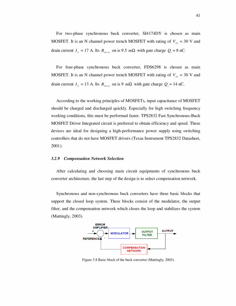
3.2.9 Compensation Network Selection
After calculating and choosing main circuit equipments of synchronous buck
converter architecture, the last step of the design is to select compensation network.
Synchronous and non-synchronous buck converters have three basic blocks that
support the closed loop system. These blocks consist of the modulator, the output
filter, and the compensation network which closes the loop and stabilizes the system
(Mattingly, 2003).
Figure 3.8 Basic block of the buck converter (Mattingly, 2003).
42
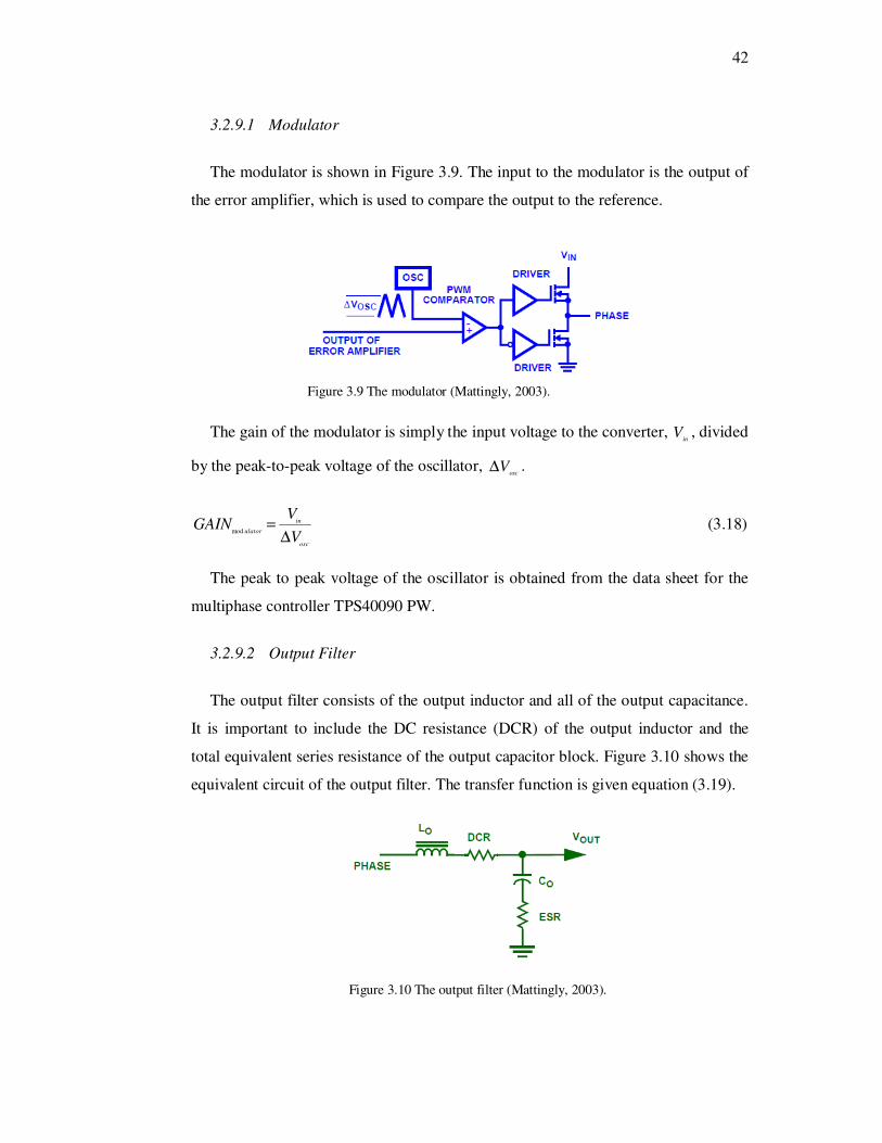
3.2.9.1 Modulator
The modulator is shown in Figure 3.9. The input to the modulator is the output of
the error amplifier, which is used to compare the output to the reference.
Figure 3.9 The modulator (Mattingly, 2003).
The gain of the modulator is simply the input voltage to the converter, in
V , divided
by the peak-to-peak voltage of the oscillator, osc
V∆ .
osc
in
ulator
V
VGAIN
∆=
mod (3.18)
The peak to peak voltage of the oscillator is obtained from the data sheet for the
multiphase controller TPS40090 PW.
3.2.9.2 Output Filter
The output filter consists of the output inductor and all of the output capacitance.
It is important to include the DC resistance (DCR) of the output inductor and the
total equivalent series resistance of the output capacitor block. Figure 3.10 shows the
equivalent circuit of the output filter. The transfer function is given equation (3.19).
Figure 3.10 The output filter (Mattingly, 2003).
43
outoutout
out
filter
CLsCDCRESRs
CESRsGAIN
⋅⋅+⋅+⋅+
⋅⋅+=
2)(1
1 (3.19)
The open loop system is shown in Figure 3.11. The transfer function is given
equation (3.20).
Figure 3.11 The open loop system (Mattingly, 2003).
outoutout
out
osc
in
openloop
CLsCDCRESRs
CESRs
V
VGAIN
⋅⋅+⋅+⋅+
⋅⋅+⋅
∆=
2)(1
1 (3.20)
Figure 3.12 The open loop system gain (Mattingly, 2003).
The resonance of the output LC filter introduces a double pole and -40dB gain
slope at Figure 3.12. The resonance frequency of the LC filter is given as:
out
PLC
CLF
×××=
π2
1)( (3.21)
The equivalent series resistance of the output capacitor and capacitance introduces
one zero for the system. The zero is expressed as follows:
44
out
ZESR
CESRF
×××=
π2
1)( (3.22)
3.2.9.3 The Compensation Network
The compensation network prevents negative effects on output voltage which are
resulted from the load changes connected to output or the change of input voltage. In
Power supply designs, compensation networks are used externally or internally.
Nowadays, the network compensations are integrated into many controller ICs.
Three different types of compensation networks used in power supply designs are
given in Figure 3.13. Generally, Type II and III are adequate to compensate the
systems.
Figure 3.13 Power supply compensation schemes
(Day, 2004).
45
TPS40090 PW multiphase controller used in two-phase and four-phase
synchronous buck converter designs has Type II and III compensation infrastructure.
3.2.9.3.1 Type II (Proportional-Integral) Compensation. The Type II
compensation network helps to shape the profile of the gain with regard to frequency
and also gives a 90° boost to the phase. Figure 3.14 shows a Type II compensation
configuration, and its asymptotic bode plot.
Figure 3.14 Type II compensation network.
46
The parameters placed in Type II compensation diagram are calculated by means
of the equations given below.
12)(
2
)(
)(R
V
V
F
DBW
F
FR
in
OSC
ZESRPLC
ZESR
⋅∆
⋅⋅
= (3.23)
R1 can be any value,
122
12
ZFR
C×⋅
=π
, )(1
75.0PLCZ
FF ⋅= (3.24)
P2FR22
11
⋅⋅=
πC ,
22
sw
P
FF = (3.25)
With Type II compensation parameters, network gain and system gain are calculated
by using equations (3.26) and (3.27).
⋅⋅
++⋅
⋅+
⋅⋅
=
212
2122
1
11
1
CCR
CCss
CRs
CRGAIN
TypeII (3.26)
TypeIIopenloopSYSTEMGAINGAINGAIN ×= (3.27)
3.2.9.3.2 Type III (Proportional-Integral-Derivative) Compensation. The Type
III compensation network shapes the profile of the gain with respect to frequency in
a similar fashion to the Type II network. The Type III compensation network,
however, utilizes two zeroes to give a phase boost of 180°. This boost is necessary to
neutralize the effects of an under damped resonance of the output filter at the double
pole. Figure 3.15 shows a Type III compensation configuration, and its asymptotic
bode plot.
47
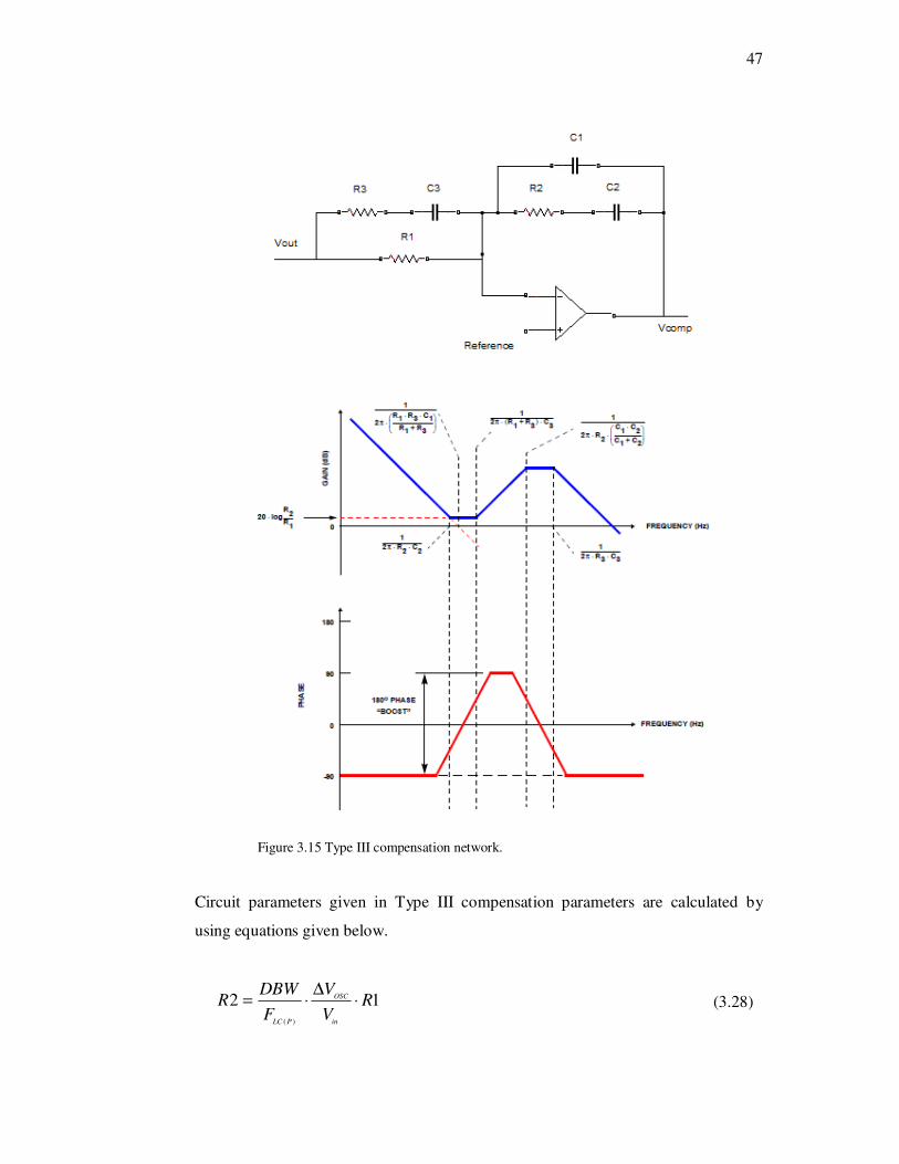
Figure 3.15 Type III compensation network.
Circuit parameters given in Type III compensation parameters are calculated by
using equations given below.
12)(
RV
V
F
DBWR
in
OSC
PLC
⋅∆
⋅= (3.28)
48
)(2
12
PLCFR
C⋅⋅
=π
(3.29)
)(22
11
ZESRFR
C⋅⋅
=π
(3.30)
12
13
)(
−⋅
=
PLC
sw
F
F
RR (3.31)
swFR
C⋅⋅
=3
13
π (3.32)
With Type III compensation parameters, network gain and system gain are calculated
by using equations (3.33) and (3.34).
( )
⋅
+⋅
⋅⋅
++⋅
⋅++⋅
⋅
+
⋅⋅⋅
+=
33
1
212
21
331
1
22
1
131
31
CRs
CCR
CCss
CRRs
CRs
CRR
RRGAIN
TypeIII (3.33)
TypeIIIopenloopSYSTEMGAINGAINGAIN ×= (3.34)
Qiao, Parto & Amirani (2002), defines typical procedure of compensator design
as;
Collect system parameters such as input voltage, output voltage, output
capacitor, etc. and determine switching frequency.
Determine the power stage poles and zeros.
Determine the bandwidth and compensation type. The compensation type is
determined by the location of bandwidth frequency as shown in Table 3.3.

49
Table 3.3 The compensation type and location of bandwidth frequency.
Compensator Type Location of Bandwidth Frequency
Type II (PI) )2()()( swBWZESRPLC
FFFF ⟨⟨⟨
Type III (PID) )2()()( swZESRBWPLC
FFFF ⟨⟨⟨
According to the first step of compensator design procedure, system parameters of
two-phase and four-phase synchronous buck converter circuits have already been
determined and calculated.
For second step of compensator design;
For two-phase synchronous buck converter circuit, according to equations (3.21)
and (3.22), power stage pole and zero values are calculated as 2.37 kHz and 126.82
kHz respectively.
For four-phase synchronous buck converter circuit, power stage pole and zero
values are calculated as 7.8 kHz and 157.5 kHz respectively.
For third step of compensator design;
In designs, stability criteria of phase and gain margin are desired to be higher than
45 degrees and 6 dB respectively (Day, 2004). For fast dynamic response, bandwidth
should be between 1/5 and 1/10 portion of switching frequency (Deng, 2005).
Consequently, for a 500 kHz switching frequency, bandwidth can be chosen a
value between 50 and 100 kHz. For both power circuits, this value is chosen as 90
kHz. It is concluded to use Type III compensation network for both two-phase and
four-phase synchronous buck converter circuits according to Table 3.3.
For both power circuits, type III compensation network parameters are calculated
by using equations (3.28), (3.29), (3.30), (3.31) and (3.32). The results are given in
Table 3.4.
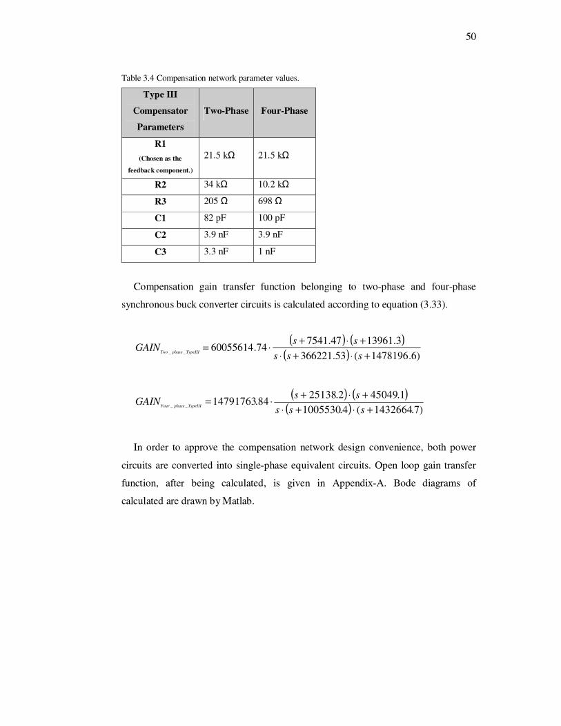
50
Table 3.4 Compensation network parameter values.
Type III
Compensator
Parameters
Two-Phase Four-Phase
R1
(Chosen as the
feedback component.)
21.5 kΩ 21.5 kΩ
R2 34 kΩ 10.2 kΩ
R3 205 Ω 698 Ω
C1 82 pF 100 pF
C2 3.9 nF 3.9 nF
C3 3.3 nF 1 nF
Compensation gain transfer function belonging to two-phase and four-phase
synchronous buck converter circuits is calculated according to equation (3.33).
( ) ( )( ) )6.1478196(53.366221
3.1396147.754174.60055614
__+⋅+⋅
+⋅+⋅=
sss
ssGAIN
TypeIIIphaseTwo
( ) ( )( ) )7.1432664(4.1005530
1.450492.2513884.14791763
__+⋅+⋅
+⋅+⋅=
sss
ssGAIN
TypeIIIphaseFour
In order to approve the compensation network design convenience, both power
circuits are converted into single-phase equivalent circuits. Open loop gain transfer
function, after being calculated, is given in Appendix-A. Bode diagrams of
calculated are drawn by Matlab.
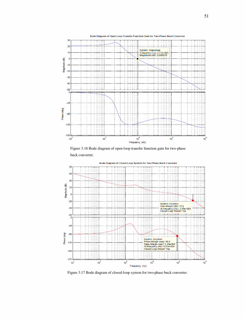
51
Figure 3.16 Bode diagram of open-loop transfer function gain for two-phase
buck converter.
Figure 3.17 Bode diagram of closed-loop system for two-phase buck converter.
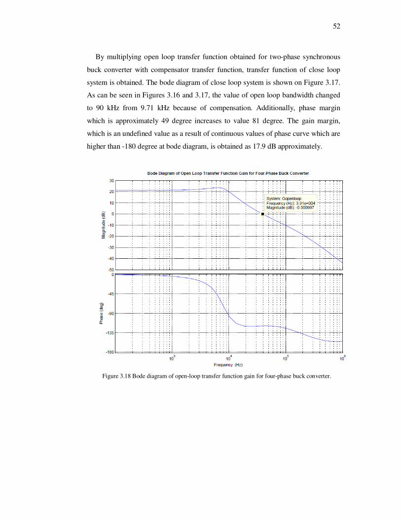
52
By multiplying open loop transfer function obtained for two-phase synchronous
buck converter with compensator transfer function, transfer function of close loop
system is obtained. The bode diagram of close loop system is shown on Figure 3.17.
As can be seen in Figures 3.16 and 3.17, the value of open loop bandwidth changed
to 90 kHz from 9.71 kHz because of compensation. Additionally, phase margin
which is approximately 49 degree increases to value 81 degree. The gain margin,
which is an undefined value as a result of continuous values of phase curve which are
higher than -180 degree at bode diagram, is obtained as 17.9 dB approximately.
Figure 3.18 Bode diagram of open-loop transfer function gain for four-phase buck converter.
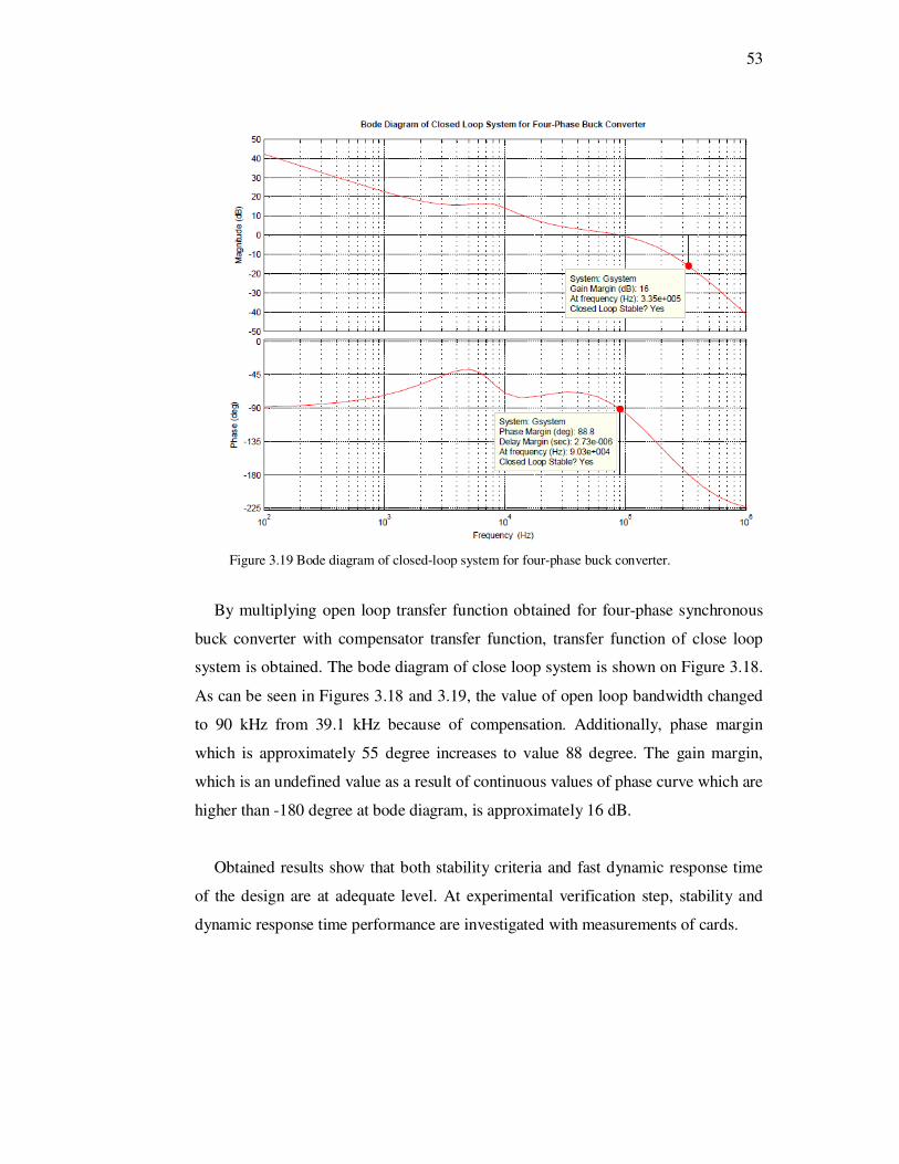
53
Figure 3.19 Bode diagram of closed-loop system for four-phase buck converter.
By multiplying open loop transfer function obtained for four-phase synchronous
buck converter with compensator transfer function, transfer function of close loop
system is obtained. The bode diagram of close loop system is shown on Figure 3.18.
As can be seen in Figures 3.18 and 3.19, the value of open loop bandwidth changed
to 90 kHz from 39.1 kHz because of compensation. Additionally, phase margin
which is approximately 55 degree increases to value 88 degree. The gain margin,
which is an undefined value as a result of continuous values of phase curve which are
higher than -180 degree at bode diagram, is approximately 16 dB.
Obtained results show that both stability criteria and fast dynamic response time
of the design are at adequate level. At experimental verification step, stability and
dynamic response time performance are investigated with measurements of cards.
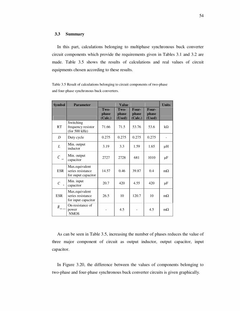
54
3.3 Summary
In this part, calculations belonging to multiphase synchronous buck converter
circuit components which provide the requirements given in Tables 3.1 and 3.2 are
made. Table 3.5 shows the results of calculations and real values of circuit
equipments chosen according to these results.
Table 3.5 Result of calculations belonging to circuit components of two-phase
and four-phase synchronous buck converters.
As can be seen in Table 3.5, increasing the number of phases reduces the value of
three major component of circuit as output inductor, output capacitor, input
capacitor.
In Figure 3.20, the difference between the values of components belonging to
two-phase and four-phase synchronous buck converter circuits is given graphically.
Symbol Parameter Value Units
Two-phase (Calc.)
Two-phase (Used)
Four-phase (Calc.)
Four-phase (Used)
RT
Switching frequency resistor (for 500 kHz)
71.66 71.5 53.76 53.6 kΩ
D Duty cycle 0.275 0.275 0.275 0.275 -
L Min. output inductor
3.19 3.3 1.59 1.65 µH
Min. output capacitor
2727 2728 681 1010 µF
ESR Max.equivalent series resistance for ouput capacitor
14.57 0.46 39.87 0.4 mΩ
Min. input capacitor
20.7 420 4.55 420 µF
ESR Max.equivalent series resistance for input capacitor
26.5 10 120.7 10 mΩ
On-resistance of power NMOS
- 4.5 - 4.5 mΩ
outC
inC
)( onDSR
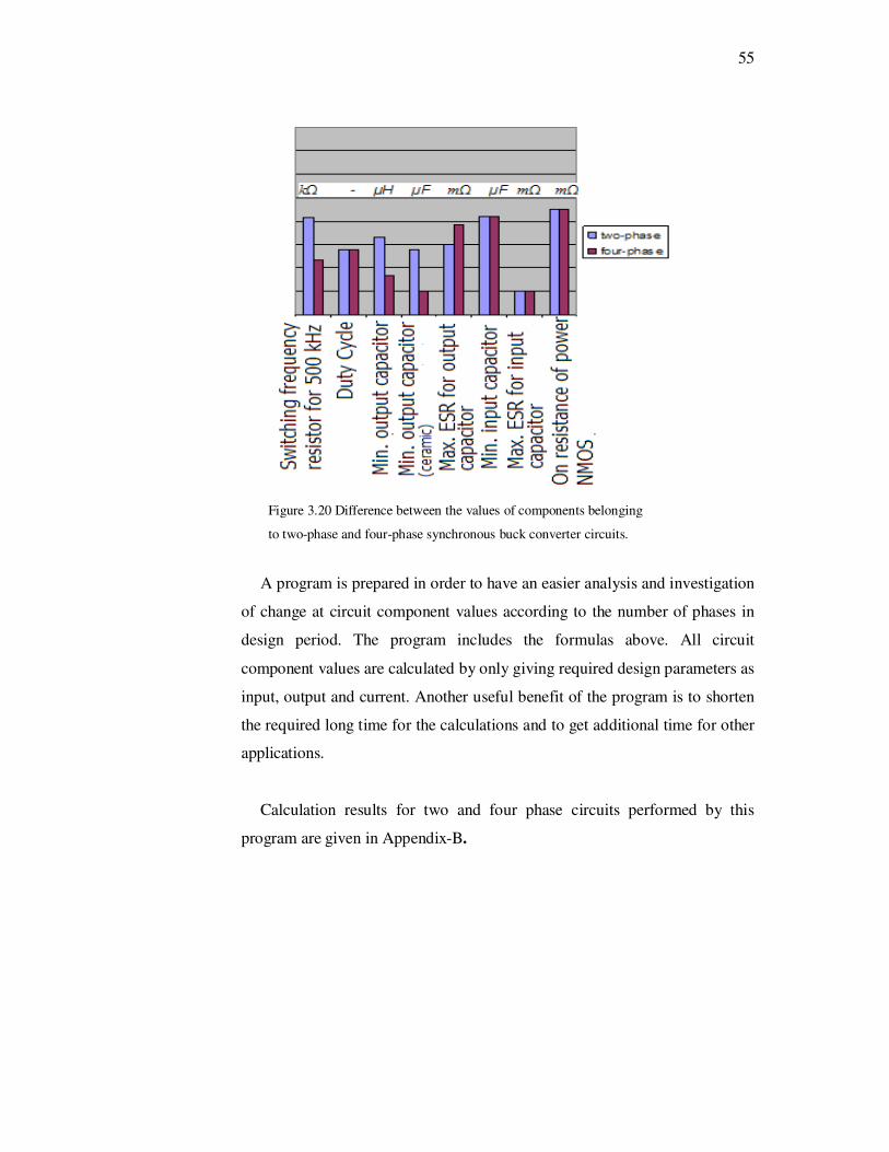
55
Figure 3.20 Difference between the values of components belonging
to two-phase and four-phase synchronous buck converter circuits.
A program is prepared in order to have an easier analysis and investigation
of change at circuit component values according to the number of phases in
design period. The program includes the formulas above. All circuit
component values are calculated by only giving required design parameters as
input, output and current. Another useful benefit of the program is to shorten
the required long time for the calculations and to get additional time for other
applications.
Calculation results for two and four phase circuits performed by this
program are given in Appendix-B.
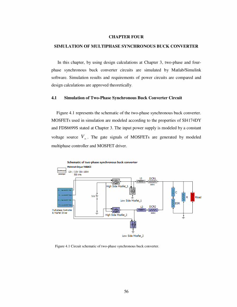
56
CHAPTER FOUR
SIMULATION OF MULTIPHASE SYNCHRONOUS BUCK CONVERTER
In this chapter, by using design calculations at Chapter 3, two-phase and four-
phase synchronous buck converter circuits are simulated by Matlab/Simulink
software. Simulation results and requirements of power circuits are compared and
design calculations are approved theoretically.
4.1 Simulation of Two-Phase Synchronous Buck Converter Circuit
Figure 4.1 represents the schematic of the two-phase synchronous buck converter.
MOSFETs used in simulation are modeled according to the properties of SI4174DY
and FDS6699S stated at Chapter 3. The input power supply is modeled by a constant
voltage source inV . The gate signals of MOSFETs are generated by modeled
multiphase controller and MOSFET driver.
Figure 4.1 Circuit schematic of two-phase synchronous buck converter.
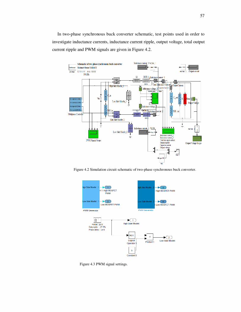
57
In two-phase synchronous buck converter schematic, test points used in order to
investigate inductance currents, inductance current ripple, output voltage, total output
current ripple and PWM signals are given in Figure 4.2.
Figure 4.2 Simulation circuit schematic of two-phase synchronous buck converter.
Figure 4.3 PWM signal settings.
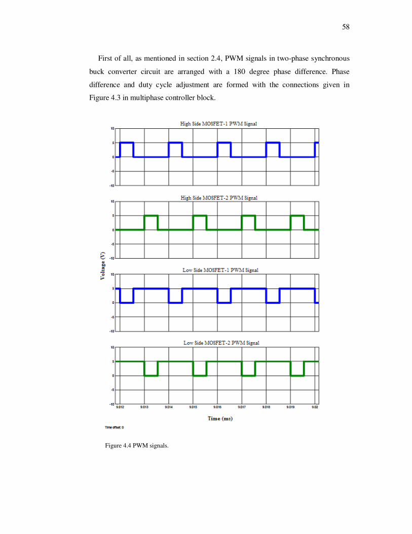
58
First of all, as mentioned in section 2.4, PWM signals in two-phase synchronous
buck converter circuit are arranged with a 180 degree phase difference. Phase
difference and duty cycle adjustment are formed with the connections given in
Figure 4.3 in multiphase controller block.
Figure 4.4 PWM signals.
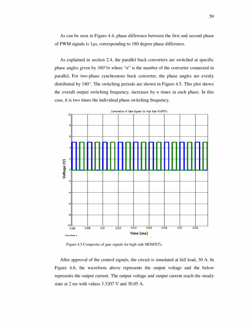
59
As can be seen in Figure 4.4, phase difference between the first and second phase
of PWM signals is 1µs, corresponding to 180 degree phase difference.
As explained in section 2.4, the parallel buck converters are switched at specific
phase angles given by 360°/n where “n” is the number of the converter connected in
parallel. For two-phase synchronous buck converter, the phase angles are evenly
distributed by 180°. The switching periods are shown in Figure 4.5. This plot shows
the overall output switching frequency, increases by n times in each phase. In this
case, it is two times the individual phase switching frequency.
Figure 4.5 Composite of gate signals for high side MOSFETs.
After approval of the control signals, the circuit is simulated at full load, 30 A. In
Figure 4.6, the waveform above represents the output voltage and the below
represents the output current. The output voltage and output current reach the steady
state at 2 ms with values 3.3207 V and 30.05 A.
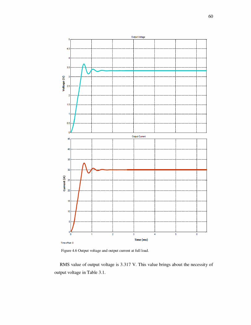
60
Figure 4.6 Output voltage and output current at full load.
RMS value of output voltage is 3.317 V. This value brings about the necessity of
output voltage in Table 3.1.
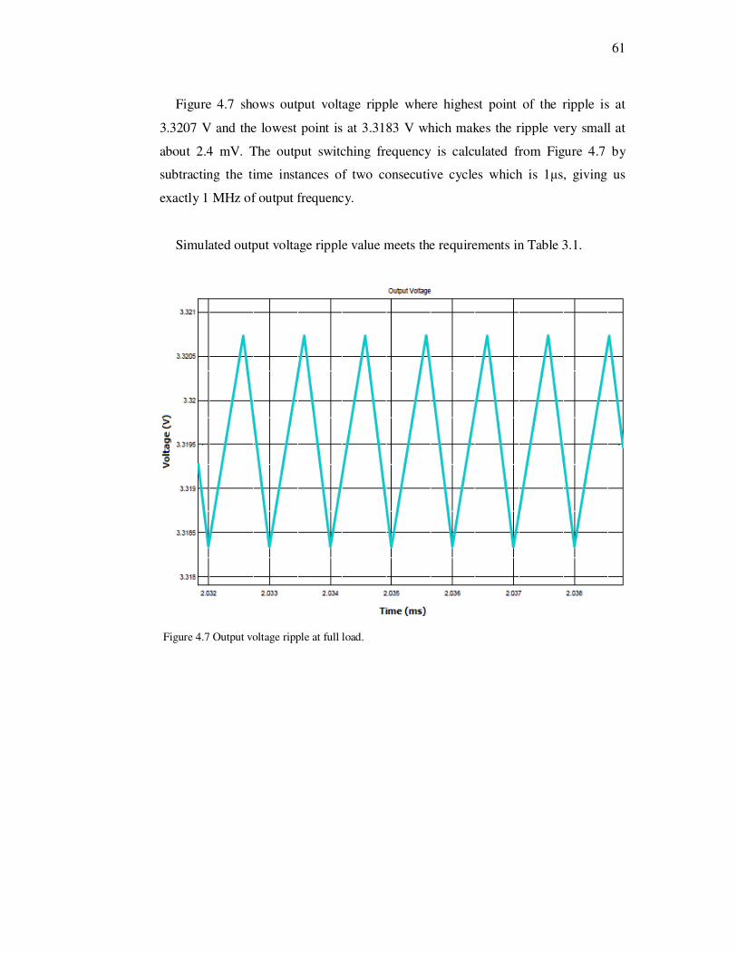
61
Figure 4.7 shows output voltage ripple where highest point of the ripple is at
3.3207 V and the lowest point is at 3.3183 V which makes the ripple very small at
about 2.4 mV. The output switching frequency is calculated from Figure 4.7 by
subtracting the time instances of two consecutive cycles which is 1µs, giving us
exactly 1 MHz of output frequency.
Simulated output voltage ripple value meets the requirements in Table 3.1.
Figure 4.7 Output voltage ripple at full load.
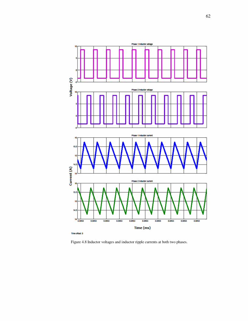
62
Figure 4.8 Inductor voltages and inductor ripple currents at both two phases.
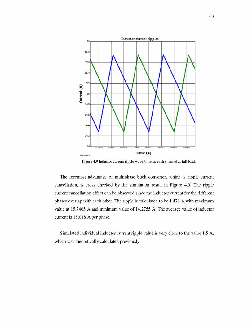
63
Figure 4.9 Inductor current ripple waveforms at each channel at full load.
The foremost advantage of multiphase buck converter, which is ripple current
cancellation, is cross checked by the simulation result in Figure 4.9. The ripple
current cancellation effect can be observed since the inductor current for the different
phases overlap with each other. The ripple is calculated to be 1.471 A with maximum
value at 15.7465 A and minimum value of 14.2755 A. The average value of inductor
current is 15.018 A per phase.
Simulated individual inductor current ripple value is very close to the value 1.5 A,
which was theoretically calculated previously.
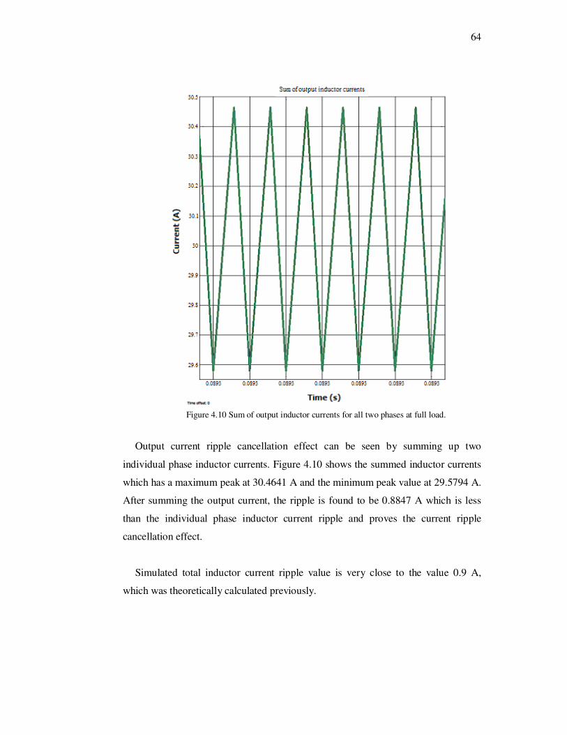
64
Figure 4.10 Sum of output inductor currents for all two phases at full load.
Output current ripple cancellation effect can be seen by summing up two
individual phase inductor currents. Figure 4.10 shows the summed inductor currents
which has a maximum peak at 30.4641 A and the minimum peak value at 29.5794 A.
After summing the output current, the ripple is found to be 0.8847 A which is less
than the individual phase inductor current ripple and proves the current ripple
cancellation effect.
Simulated total inductor current ripple value is very close to the value 0.9 A,
which was theoretically calculated previously.
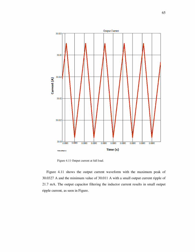
65
Figure 4.11 Output current at full load.
Figure 4.11 shows the output current waveform with the maximum peak of
30.0327 A and the minimum value of 30.011 A with a small output current ripple of
21.7 mA. The output capacitor filtering the inductor current results in small output
ripple current, as seen in Figure.
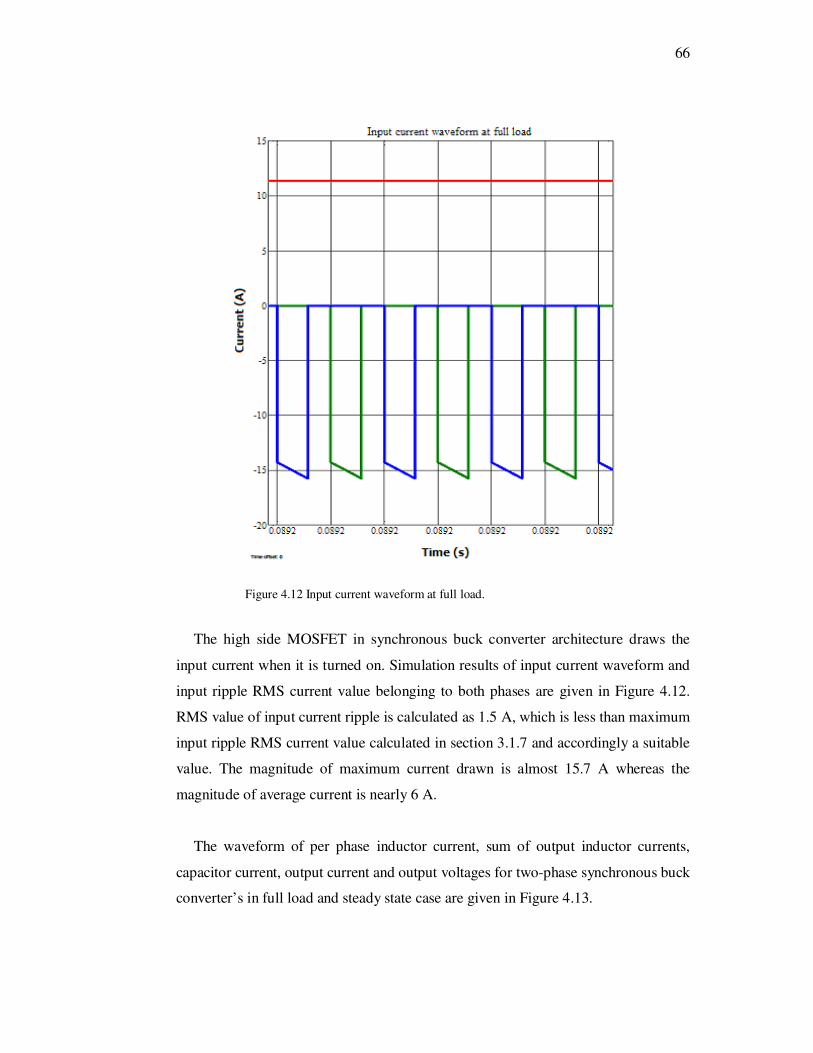
66
Figure 4.12 Input current waveform at full load.
The high side MOSFET in synchronous buck converter architecture draws the
input current when it is turned on. Simulation results of input current waveform and
input ripple RMS current value belonging to both phases are given in Figure 4.12.
RMS value of input current ripple is calculated as 1.5 A, which is less than maximum
input ripple RMS current value calculated in section 3.1.7 and accordingly a suitable
value. The magnitude of maximum current drawn is almost 15.7 A whereas the
magnitude of average current is nearly 6 A.
The waveform of per phase inductor current, sum of output inductor currents,
capacitor current, output current and output voltages for two-phase synchronous buck
converter’s in full load and steady state case are given in Figure 4.13.
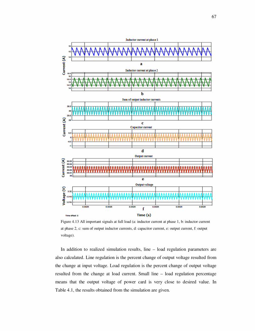
67
Figure 4.13 All important signals at full load (a: inductor current at phase 1, b: inductor current
at phase 2, c: sum of output inductor currents, d: capacitor current, e: output current, f: output
voltage).
In addition to realized simulation results, line – load regulation parameters are
also calculated. Line regulation is the percent change of output voltage resulted from
the change at input voltage. Load regulation is the percent change of output voltage
resulted from the change at load current. Small line – load regulation percentage
means that the output voltage of power card is very close to desired value. In
Table 4.1, the results obtained from the simulation are given.
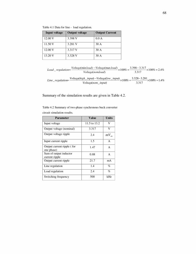
68
Table 4.1 Data for line - load regulation.
Input voltage Output voltage Output Current
12.00 V 3.398 V 0.0 A
11.50 V 3.281 V 30 A
12.00 V 3.317 V 30 A
13.20 V 3.328 V 30 A
%4.2%100317.3
317.3398.3%100
).(
)(max)(min_ =×
−=×
−=
loadnomVoltage
loadVoltageloadVoltageregulationLoad
%4.1%100317.3
281.3328.3%100
)_(
)_()_(_ =×
−=×
−=
inputnomVoltage
inputlowVoltageinputhighVoltageregulationLine
Summary of the simulation results are given in Table 4.2.
Table 4.2 Summary of two-phase synchronous buck converter
circuit simulation results.
Parameter Value Units
Input voltage 11.5 to 13.2 V
Output voltage (nominal) 3.317 V
Output voltage ripple 2.4 PK
mV
Input current ripple 1.5 A
Output current ripple ( for one phase)
1.47 A
Sum of output inductor current ripple
0.88 A
Output current ripple 21.7 mA
Line regulation 1.4 %
Load regulation 2.4 %
Switching frequency 500 kHz
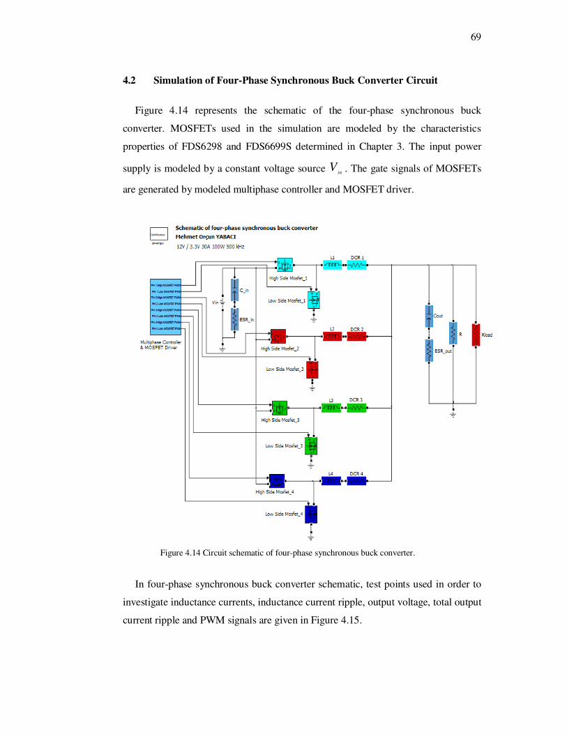
69
4.2 Simulation of Four-Phase Synchronous Buck Converter Circuit
Figure 4.14 represents the schematic of the four-phase synchronous buck
converter. MOSFETs used in the simulation are modeled by the characteristics
properties of FDS6298 and FDS6699S determined in Chapter 3. The input power
supply is modeled by a constant voltage source inV . The gate signals of MOSFETs
are generated by modeled multiphase controller and MOSFET driver.
Figure 4.14 Circuit schematic of four-phase synchronous buck converter.
In four-phase synchronous buck converter schematic, test points used in order to
investigate inductance currents, inductance current ripple, output voltage, total output
current ripple and PWM signals are given in Figure 4.15.
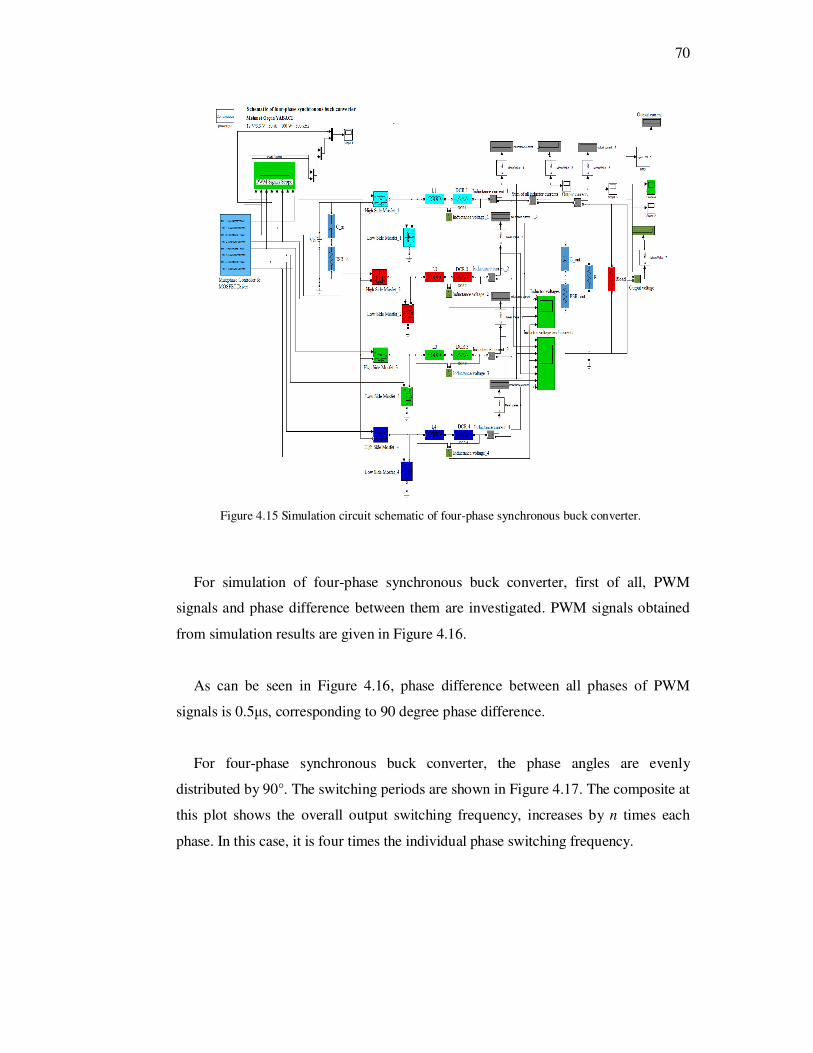
70
Figure 4.15 Simulation circuit schematic of four-phase synchronous buck converter.
For simulation of four-phase synchronous buck converter, first of all, PWM
signals and phase difference between them are investigated. PWM signals obtained
from simulation results are given in Figure 4.16.
As can be seen in Figure 4.16, phase difference between all phases of PWM
signals is 0.5µs, corresponding to 90 degree phase difference.
For four-phase synchronous buck converter, the phase angles are evenly
distributed by 90°. The switching periods are shown in Figure 4.17. The composite at
this plot shows the overall output switching frequency, increases by n times each
phase. In this case, it is four times the individual phase switching frequency.
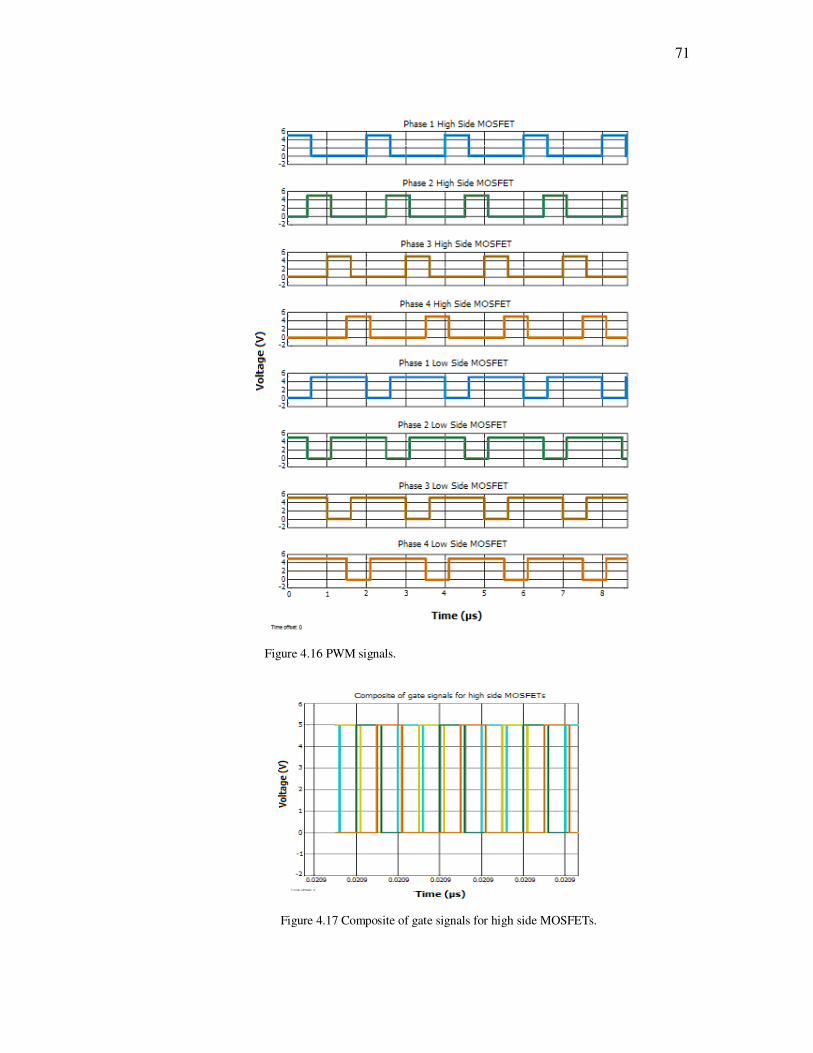
71
Figure 4.16 PWM signals.
Figure 4.17 Composite of gate signals for high side MOSFETs.
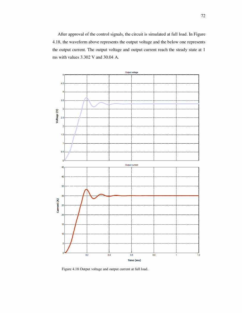
72
After approval of the control signals, the circuit is simulated at full load. In Figure
4.18, the waveform above represents the output voltage and the below one represents
the output current. The output voltage and output current reach the steady state at 1
ms with values 3.302 V and 30.04 A.
Figure 4.18 Output voltage and output current at full load.
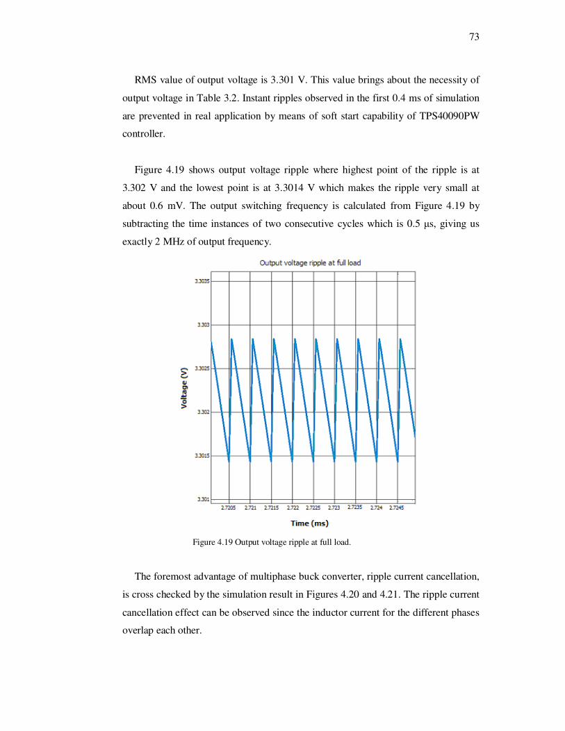
73
RMS value of output voltage is 3.301 V. This value brings about the necessity of
output voltage in Table 3.2. Instant ripples observed in the first 0.4 ms of simulation
are prevented in real application by means of soft start capability of TPS40090PW
controller.
Figure 4.19 shows output voltage ripple where highest point of the ripple is at
3.302 V and the lowest point is at 3.3014 V which makes the ripple very small at
about 0.6 mV. The output switching frequency is calculated from Figure 4.19 by
subtracting the time instances of two consecutive cycles which is 0.5 µs, giving us
exactly 2 MHz of output frequency.
Figure 4.19 Output voltage ripple at full load.
The foremost advantage of multiphase buck converter, ripple current cancellation,
is cross checked by the simulation result in Figures 4.20 and 4.21. The ripple current
cancellation effect can be observed since the inductor current for the different phases
overlap each other.
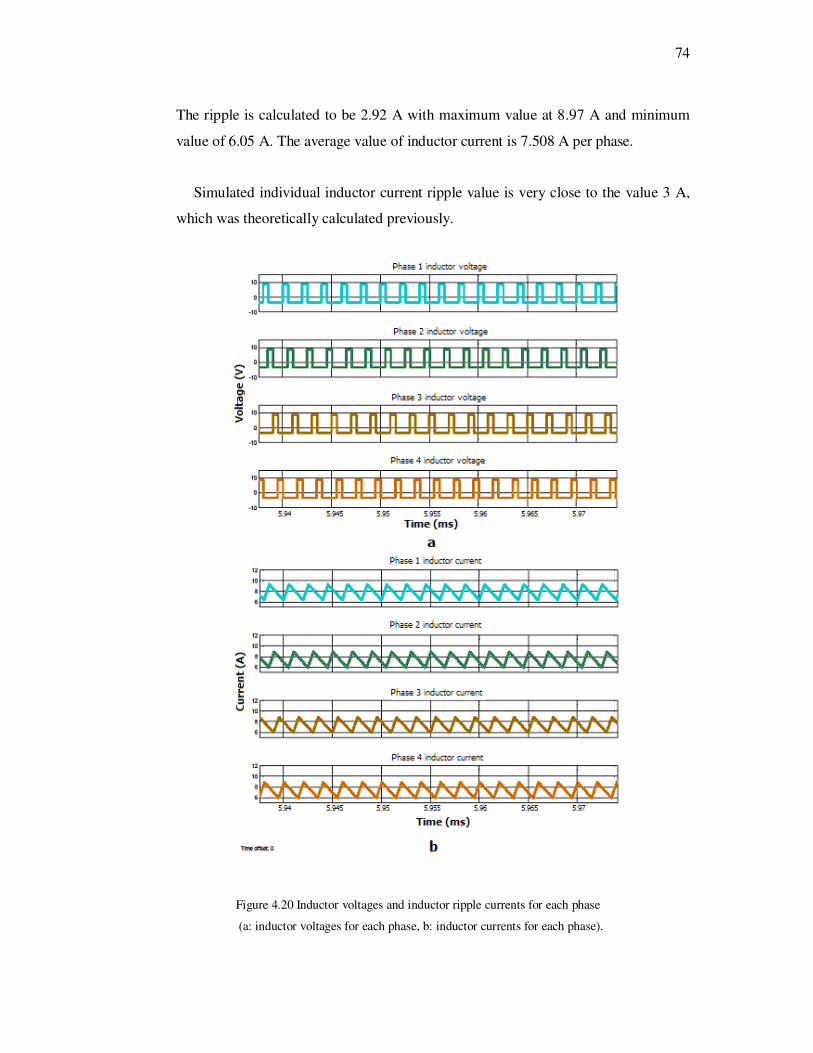
74
The ripple is calculated to be 2.92 A with maximum value at 8.97 A and minimum
value of 6.05 A. The average value of inductor current is 7.508 A per phase.
Simulated individual inductor current ripple value is very close to the value 3 A,
which was theoretically calculated previously.
Figure 4.20 Inductor voltages and inductor ripple currents for each phase
(a: inductor voltages for each phase, b: inductor currents for each phase).
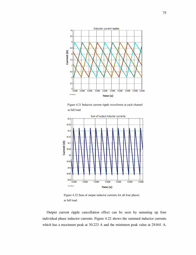
75
Figure 4.21 Inductor current ripple waveforms at each channel
at full load.
Figure 4.22 Sum of output inductor currents for all four phases
at full load.
Output current ripple cancellation effect can be seen by summing up four
individual phase inductor currents. Figure 4.22 shows the summed inductor currents
which has a maximum peak at 30.223 A and the minimum peak value at 29.841 A.
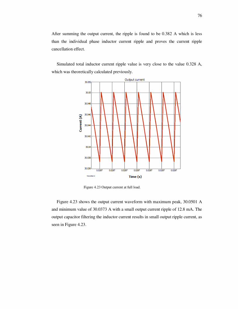
76
After summing the output current, the ripple is found to be 0.382 A which is less
than the individual phase inductor current ripple and proves the current ripple
cancellation effect.
Simulated total inductor current ripple value is very close to the value 0.328 A,
which was theoretically calculated previously.
Figure 4.23 Output current at full load.
Figure 4.23 shows the output current waveform with maximum peak, 30.0501 A
and minimum value of 30.0373 A with a small output current ripple of 12.8 mA. The
output capacitor filtering the inductor current results in small output ripple current, as
seen in Figure 4.23.
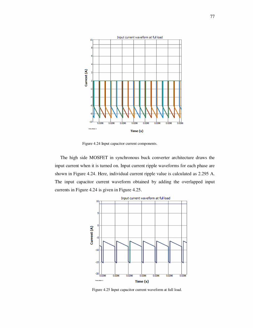
77
Figure 4.24 Input capacitor current components.
The high side MOSFET in synchronous buck converter architecture draws the
input current when it is turned on. Input current ripple waveforms for each phase are
shown in Figure 4.24. Here, individual current ripple value is calculated as 2.295 A.
The input capacitor current waveform obtained by adding the overlapped input
currents in Figure 4.24 is given in Figure 4.25.
Figure 4.25 Input capacitor current waveform at full load.
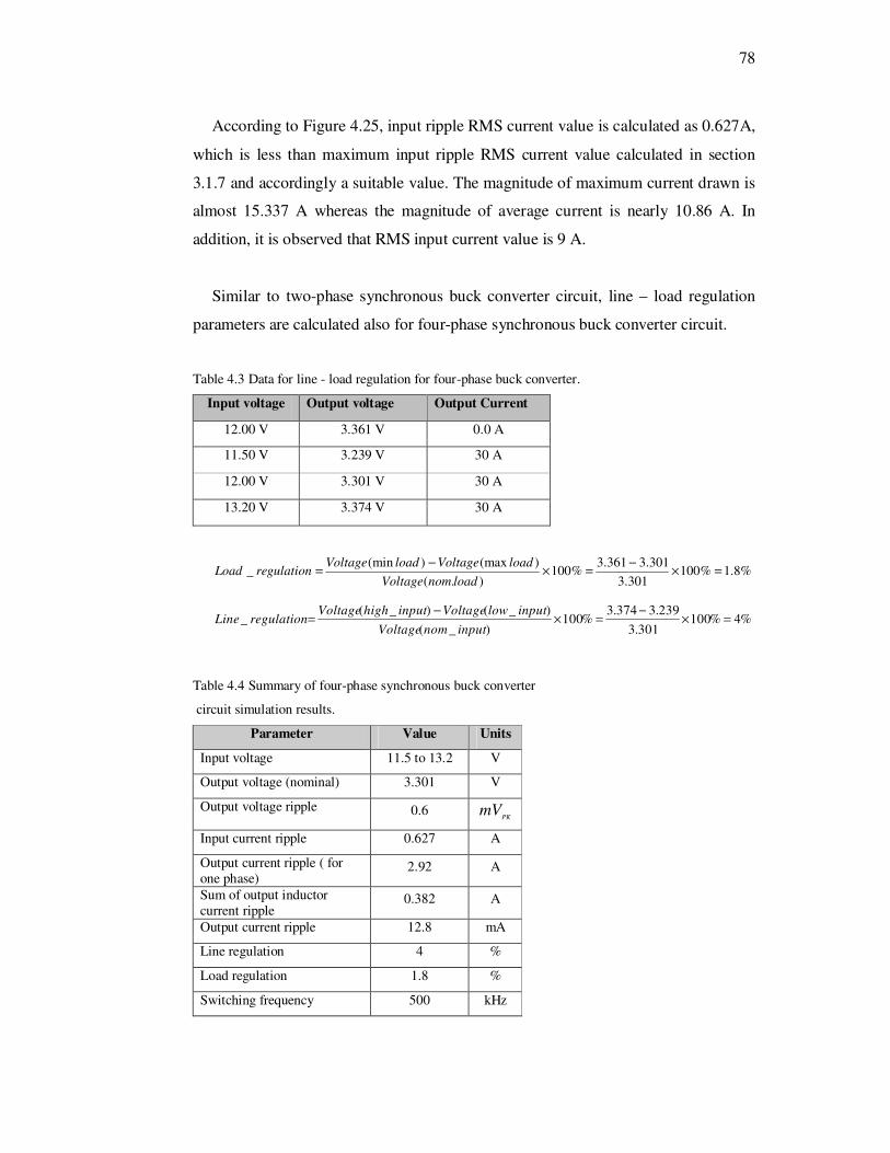
78
According to Figure 4.25, input ripple RMS current value is calculated as 0.627A,
which is less than maximum input ripple RMS current value calculated in section
3.1.7 and accordingly a suitable value. The magnitude of maximum current drawn is
almost 15.337 A whereas the magnitude of average current is nearly 10.86 A. In
addition, it is observed that RMS input current value is 9 A.
Similar to two-phase synchronous buck converter circuit, line – load regulation
parameters are calculated also for four-phase synchronous buck converter circuit.
Table 4.3 Data for line - load regulation for four-phase buck converter.
Input voltage Output voltage Output Current
12.00 V 3.361 V 0.0 A
11.50 V 3.239 V 30 A
12.00 V 3.301 V 30 A
13.20 V 3.374 V 30 A
%8.1%100301.3
301.3361.3%100
).(
)(max)(min_ =×
−=×
−=
loadnomVoltage
loadVoltageloadVoltageregulationLoad
%4%100301.3
239.3374.3%100
)_(
)_()_(_ =×
−=×
−=
inputnomVoltage
inputlowVoltageinputhighVoltageregulationLine
Table 4.4 Summary of four-phase synchronous buck converter
circuit simulation results.
Parameter Value Units
Input voltage 11.5 to 13.2 V
Output voltage (nominal) 3.301 V
Output voltage ripple 0.6 PK
mV
Input current ripple 0.627 A
Output current ripple ( for one phase)
2.92 A
Sum of output inductor current ripple
0.382 A
Output current ripple 12.8 mA
Line regulation 4 %
Load regulation 1.8 %
Switching frequency 500 kHz
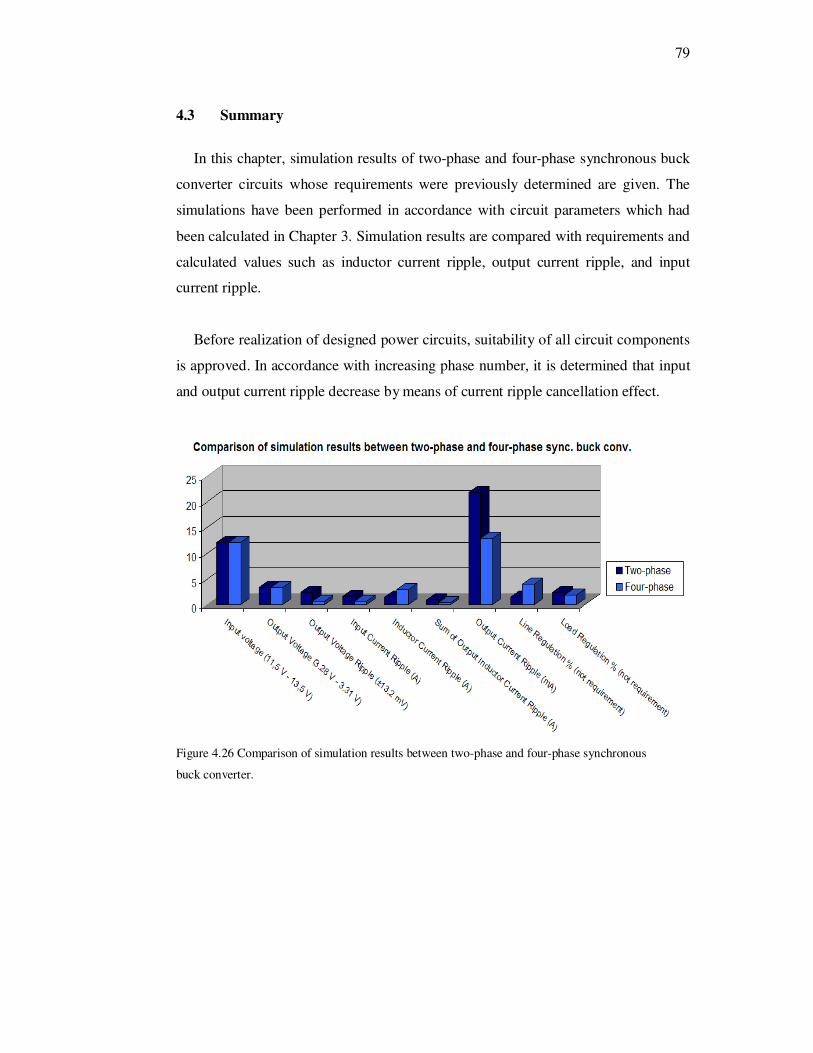
79
4.3 Summary
In this chapter, simulation results of two-phase and four-phase synchronous buck
converter circuits whose requirements were previously determined are given. The
simulations have been performed in accordance with circuit parameters which had
been calculated in Chapter 3. Simulation results are compared with requirements and
calculated values such as inductor current ripple, output current ripple, and input
current ripple.
Before realization of designed power circuits, suitability of all circuit components
is approved. In accordance with increasing phase number, it is determined that input
and output current ripple decrease by means of current ripple cancellation effect.
Figure 4.26 Comparison of simulation results between two-phase and four-phase synchronous
buck converter.
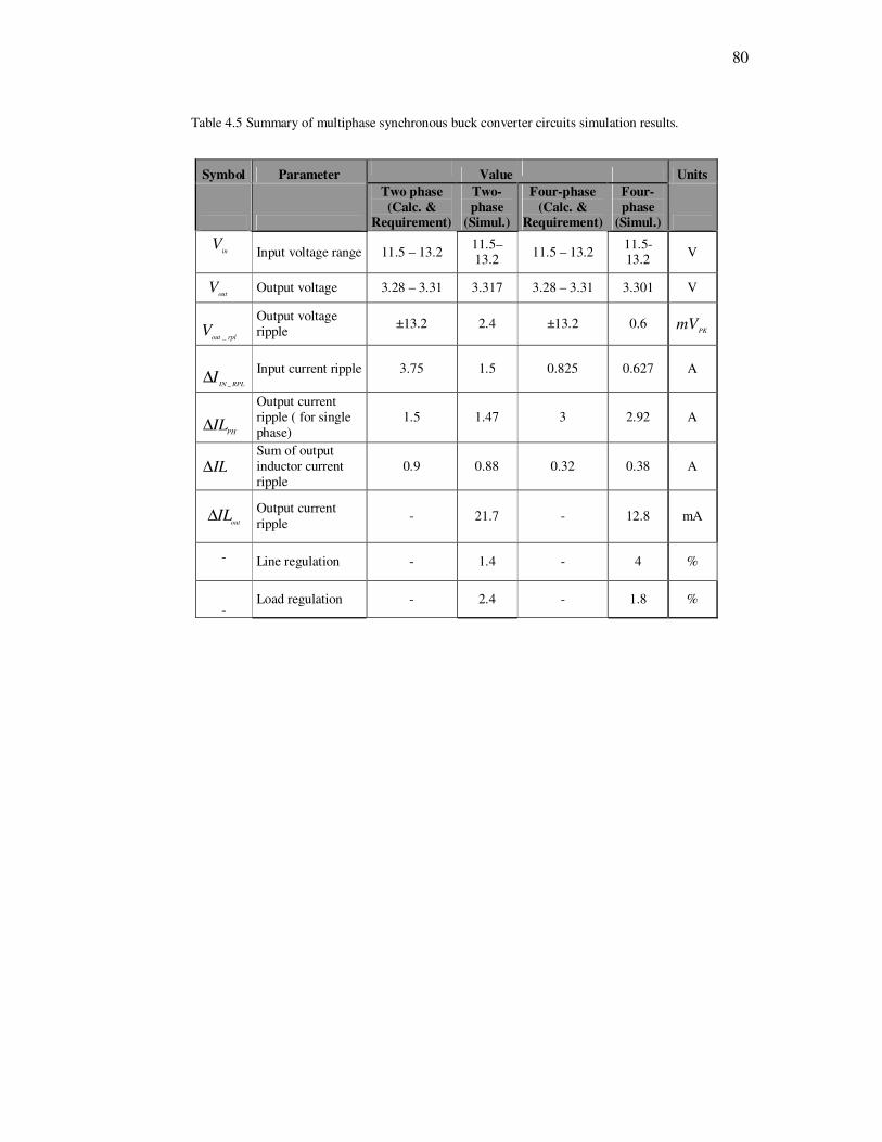
80
Table 4.5 Summary of multiphase synchronous buck converter circuits simulation results.
Symbol Parameter Value Units
Two phase (Calc. &
Requirement)
Two-phase
(Simul.)
Four-phase (Calc. &
Requirement)
Four-phase
(Simul.)
in
V
Input voltage range 11.5 – 13.2
11.5–13.2
11.5 – 13.2 11.5-13.2
V
out
V Output voltage 3.28 – 3.31 3.317 3.28 – 3.31 3.301 V
rploutV
_
Output voltage ripple
±13.2 2.4 ±13.2 0.6 PK
mV
RPLINI
_∆
Input current ripple 3.75 1.5 0.825 0.627 A
PHIL∆
Output current ripple ( for single phase)
1.5 1.47 3 2.92 A
IL∆
Sum of output inductor current ripple
0.9 0.88 0.32 0.38 A
outIL∆
Output current ripple
- 21.7 - 12.8 mA
-
Line regulation - 1.4 - 4 %
- Load regulation - 2.4 - 1.8 %

81
CHAPTER FIVE
EXPERIMENTAL VERIFICATION
In this chapter, experimental verification of designed two-phase and four-phase
synchronous buck converter circuits is explained. Schematic and printed circuit
boards drawings are given. The total costs of designed circuits are calculated and
analyzed.
5.1 Design of Printed Circuit Board (PCB)
The schematics of designed two-phase and four-phase synchronous buck
converter circuits are drawn by using Proteus ISIS 7 and ExpressSCH programs. The
schematics are given in Appendix-C. The schematic contains the circuits listed
below:
Multiphase Controller Circuit
Gate Driver Circuit
Power Circuit
Multiphase Controller Circuit only includes TPS40090 PW controller. Schematic
of multiphase controller circuit is given in Figure 5.1.
Figure 5.1 Schematic of the multiphase controller TPS40090.
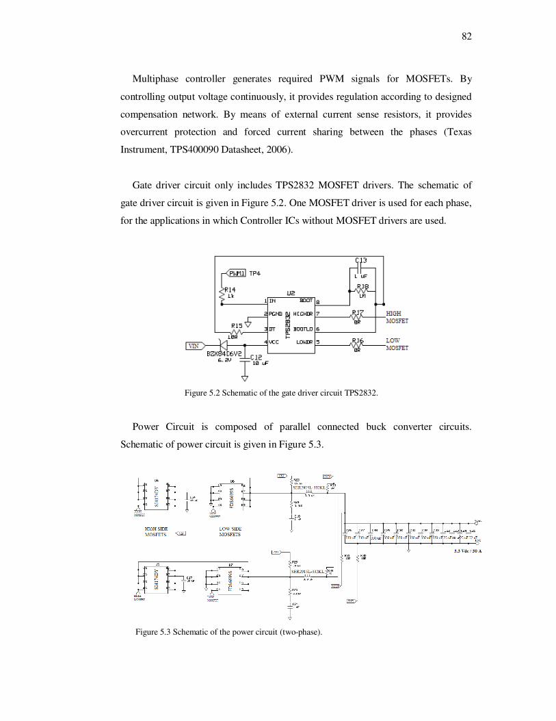
82
Multiphase controller generates required PWM signals for MOSFETs. By
controlling output voltage continuously, it provides regulation according to designed
compensation network. By means of external current sense resistors, it provides
overcurrent protection and forced current sharing between the phases (Texas
Instrument, TPS400090 Datasheet, 2006).
Gate driver circuit only includes TPS2832 MOSFET drivers. The schematic of
gate driver circuit is given in Figure 5.2. One MOSFET driver is used for each phase,
for the applications in which Controller ICs without MOSFET drivers are used.
Figure 5.2 Schematic of the gate driver circuit TPS2832.
Power Circuit is composed of parallel connected buck converter circuits.
Schematic of power circuit is given in Figure 5.3.
Figure 5.3 Schematic of the power circuit (two-phase).
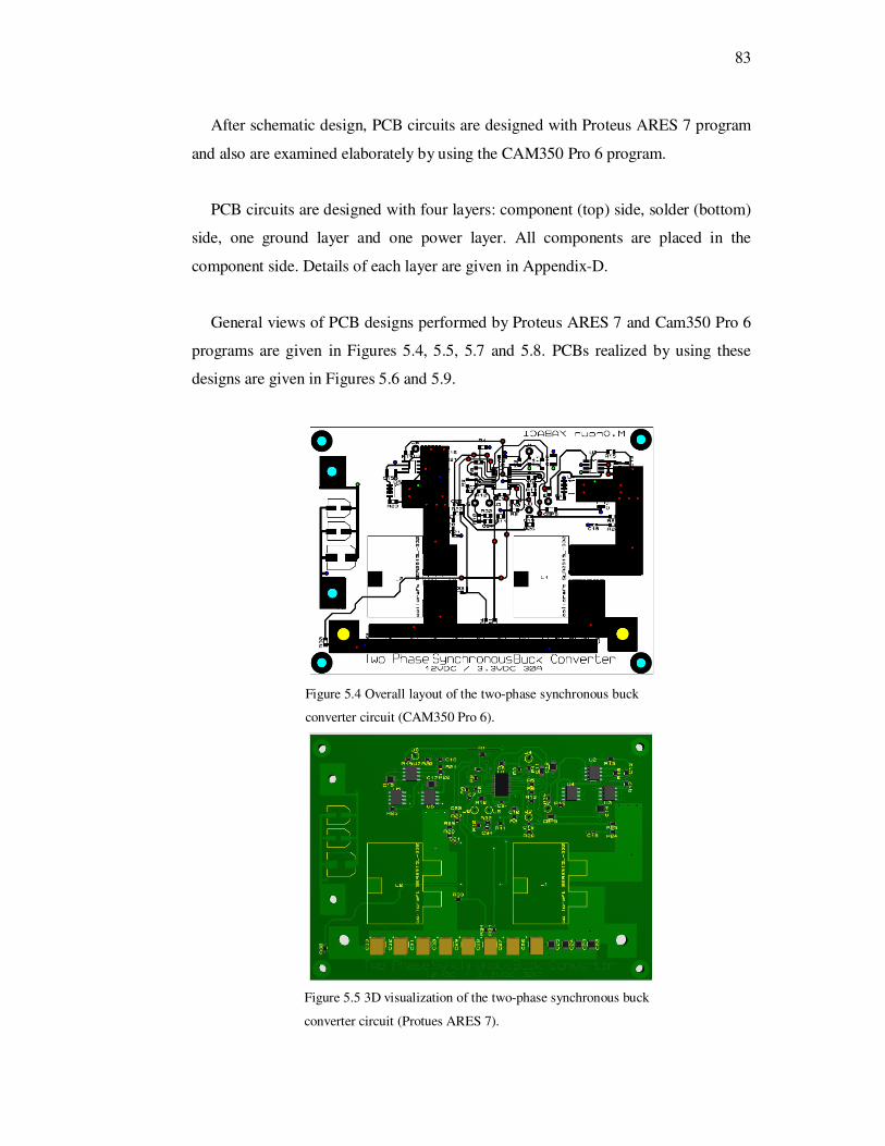
83
After schematic design, PCB circuits are designed with Proteus ARES 7 program
and also are examined elaborately by using the CAM350 Pro 6 program.
PCB circuits are designed with four layers: component (top) side, solder (bottom)
side, one ground layer and one power layer. All components are placed in the
component side. Details of each layer are given in Appendix-D.
General views of PCB designs performed by Proteus ARES 7 and Cam350 Pro 6
programs are given in Figures 5.4, 5.5, 5.7 and 5.8. PCBs realized by using these
designs are given in Figures 5.6 and 5.9.
Figure 5.4 Overall layout of the two-phase synchronous buck
converter circuit (CAM350 Pro 6).
Figure 5.5 3D visualization of the two-phase synchronous buck
converter circuit (Protues ARES 7).
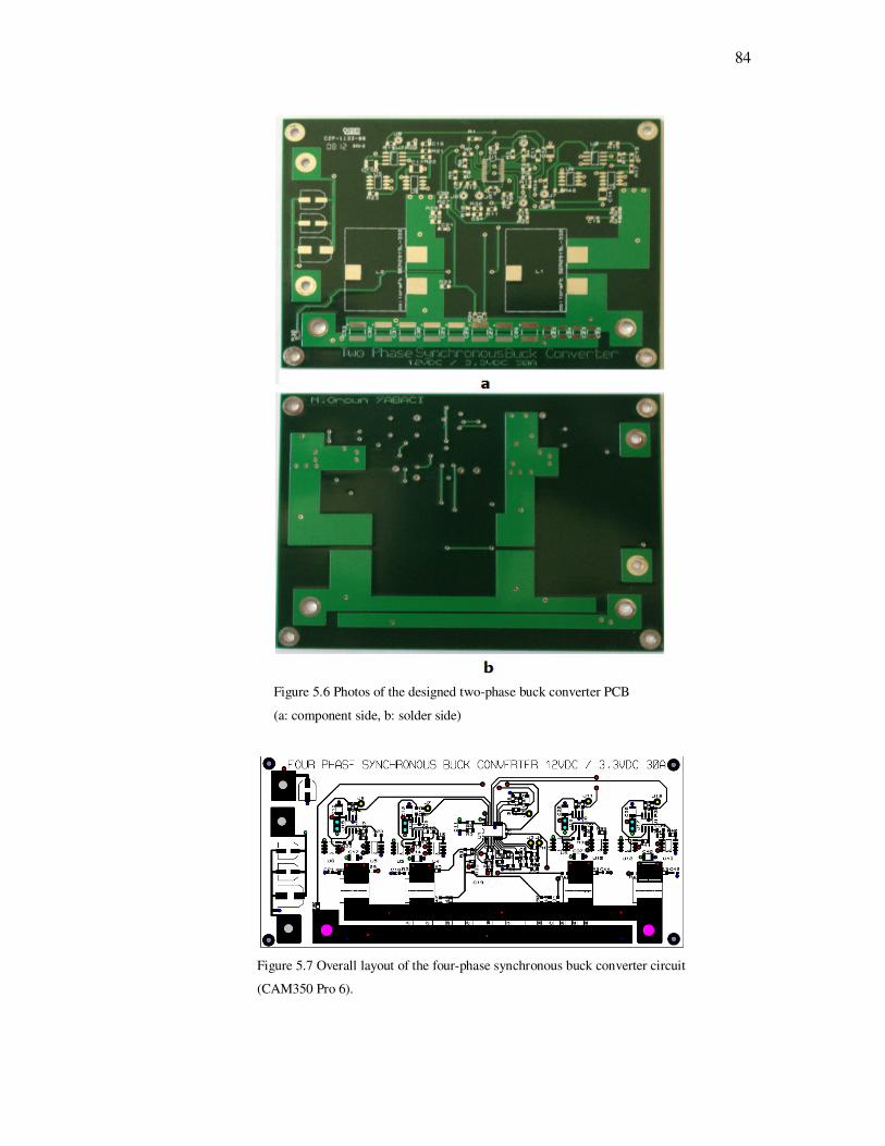
84
Figure 5.6 Photos of the designed two-phase buck converter PCB
(a: component side, b: solder side)
Figure 5.7 Overall layout of the four-phase synchronous buck converter circuit
(CAM350 Pro 6).
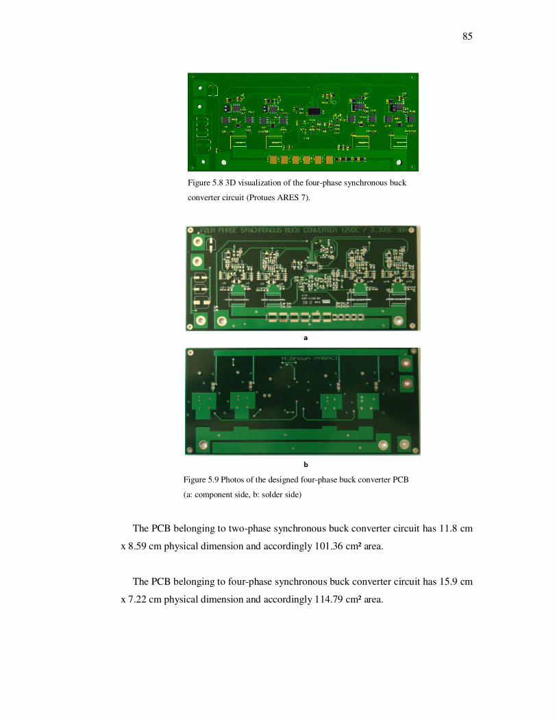
85
Figure 5.8 3D visualization of the four-phase synchronous buck
converter circuit (Protues ARES 7).
Figure 5.9 Photos of the designed four-phase buck converter PCB
(a: component side, b: solder side)
The PCB belonging to two-phase synchronous buck converter circuit has 11.8 cm
x 8.59 cm physical dimension and accordingly 101.36 cm² area.
The PCB belonging to four-phase synchronous buck converter circuit has 15.9 cm
x 7.22 cm physical dimension and accordingly 114.79 cm² area.
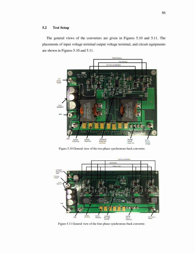
86
5.2 Test Setup
The general views of the converters are given in Figures 5.10 and 5.11. The
placements of input voltage terminal output voltage terminal, and circuit equipments
are shown in Figures 5.10 and 5.11.
Figure 5.10 General view of the two-phase synchronous buck converter.
Figure 5.11 General view of the four-phase synchronous buck converter.
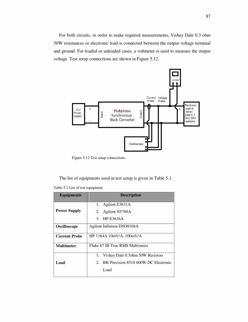
87
For both circuits, in order to make required measurements, Vishay Dale 0.3 ohm
50W resistances or electronic load is connected between the output voltage terminal
and ground. For loaded or unloaded cases, a voltmeter is used to measure the output
voltage. Test setup connections are shown in Figure 5.12.
Figure 5.12 Test setup connections.
The list of equipments used in test setup is given in Table 5.1.
Table 5.1 List of test equipment.
Equipments Description
Power Supply
1. Agilent E3631A
2. Agilent N5769A
3. HP E3616A
Oscilloscope Agilent Infinium DSO8104A
Current Probe HP 1164A 10mV/A, 100mV/A
Multimeter Fluke 87 III True RMS Multimeter
Load
1. Vishay Dale 0.3ohm 50W Resistors
2. BK Precision 8510 600W DC Electronic
Load
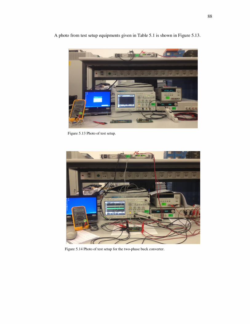
88
A photo from test setup equipments given in Table 5.1 is shown in Figure 5.13.
Figure 5.13 Photo of test setup.
Figure 5.14 Photo of test setup for the two-phase buck converter.
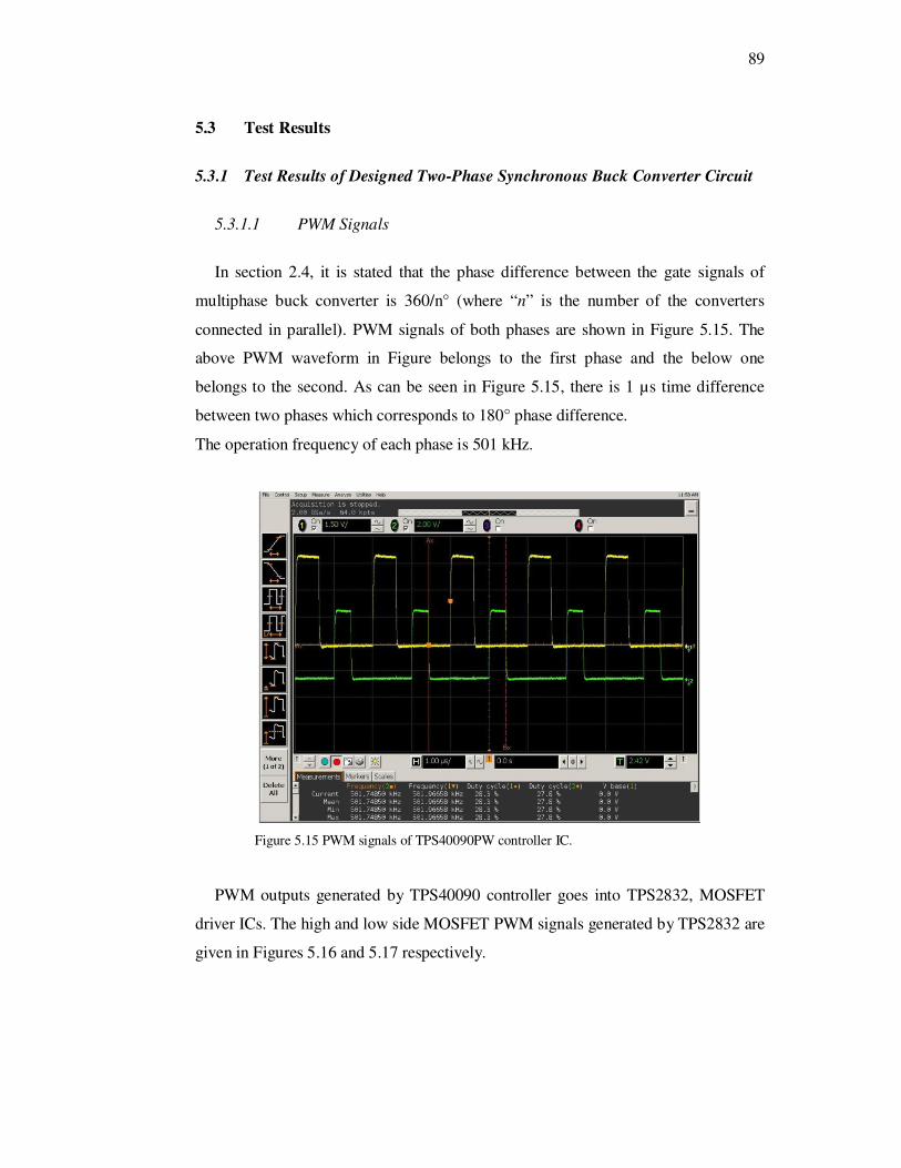
89
5.3 Test Results
5.3.1 Test Results of Designed Two-Phase Synchronous Buck Converter Circuit
5.3.1.1 PWM Signals
In section 2.4, it is stated that the phase difference between the gate signals of
multiphase buck converter is 360/n° (where “n” is the number of the converters
connected in parallel). PWM signals of both phases are shown in Figure 5.15. The
above PWM waveform in Figure belongs to the first phase and the below one
belongs to the second. As can be seen in Figure 5.15, there is 1 µs time difference
between two phases which corresponds to 180° phase difference.
The operation frequency of each phase is 501 kHz.
Figure 5.15 PWM signals of TPS40090PW controller IC.
PWM outputs generated by TPS40090 controller goes into TPS2832, MOSFET
driver ICs. The high and low side MOSFET PWM signals generated by TPS2832 are
given in Figures 5.16 and 5.17 respectively.
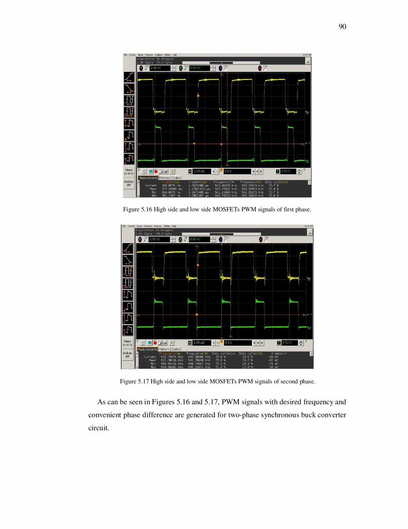
90
Figure 5.16 High side and low side MOSFETs PWM signals of first phase.
Figure 5.17 High side and low side MOSFETs PWM signals of second phase.
As can be seen in Figures 5.16 and 5.17, PWM signals with desired frequency and
convenient phase difference are generated for two-phase synchronous buck converter
circuit.
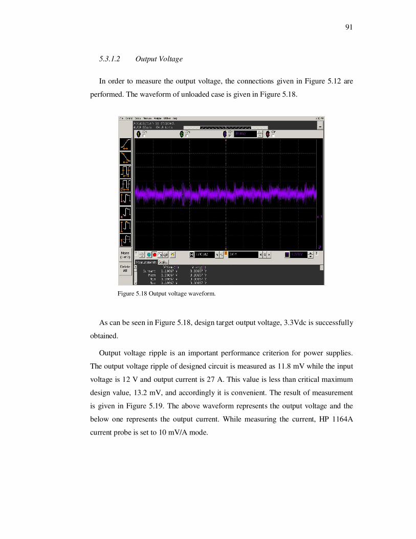
91
5.3.1.2 Output Voltage
In order to measure the output voltage, the connections given in Figure 5.12 are
performed. The waveform of unloaded case is given in Figure 5.18.
Figure 5.18 Output voltage waveform.
As can be seen in Figure 5.18, design target output voltage, 3.3Vdc is successfully
obtained.
Output voltage ripple is an important performance criterion for power supplies.
The output voltage ripple of designed circuit is measured as 11.8 mV while the input
voltage is 12 V and output current is 27 A. This value is less than critical maximum
design value, 13.2 mV, and accordingly it is convenient. The result of measurement
is given in Figure 5.19. The above waveform represents the output voltage and the
below one represents the output current. While measuring the current, HP 1164A
current probe is set to 10 mV/A mode.
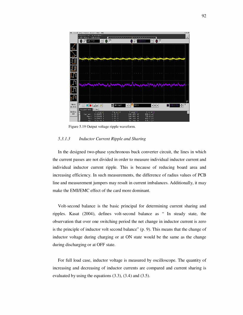
92
Figure 5.19 Output voltage ripple waveform.
5.3.1.3 Inductor Current Ripple and Sharing
In the designed two-phase synchronous buck converter circuit, the lines in which
the current passes are not divided in order to measure individual inductor current and
individual inductor current ripple. This is because of reducing board area and
increasing efficiency. In such measurements, the difference of radius values of PCB
line and measurement jumpers may result in current imbalances. Additionally, it may
make the EMI/EMC effect of the card more dominant.
Volt-second balance is the basic principal for determining current sharing and
ripples. Kasat (2004), defines volt-second balance as “ In steady state, the
observation that over one switching period the net change in inductor current is zero
is the principle of inductor volt second balance” (p. 9). This means that the change of
inductor voltage during charging or at ON state would be the same as the change
during discharging or at OFF state.
For full load case, inductor voltage is measured by oscilloscope. The quantity of
increasing and decreasing of inductor currents are compared and current sharing is
evaluated by using the equations (3.3), (3.4) and (3.5).
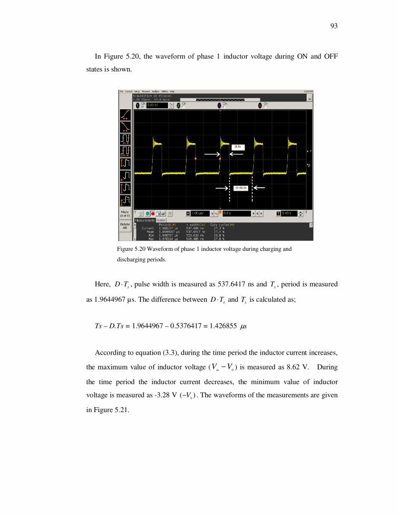
93
In Figure 5.20, the waveform of phase 1 inductor voltage during ON and OFF
states is shown.
Figure 5.20 Waveform of phase 1 inductor voltage during charging and
discharging periods.
Here, S
TD ⋅ , pulse width is measured as 537.6417 ns and S
T , period is measured
as 1.9644967 µs. The difference between S
TD ⋅ and S
T is calculated as;
Ts – D.Ts = 1.9644967 – 0.5376417 = 1.426855 sµ
According to equation (3.3), during the time period the inductor current increases,
the maximum value of inductor voltage ( 0VV
in− ) is measured as 8.62 V. During
the time period the inductor current decreases, the minimum value of inductor
voltage is measured as -3.28 V )(0
V− . The waveforms of the measurements are given
in Figure 5.21.
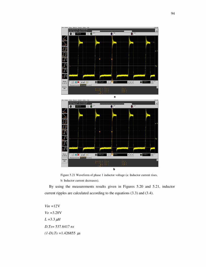
94
Figure 5.21 Waveform of phase 1 inductor voltage (a: Inductor current rises,
b: Inductor current decreases).
By using the measurements results given in Figures 5.20 and 5.21, inductor
current ripples are calculated according to the equations (3.3) and (3.4).
Vin =12V
Vo =3.28V
L =3.3 Hµ
D.Ts= 537.6417 ns
(1-D).Ts =1.426855 sµ
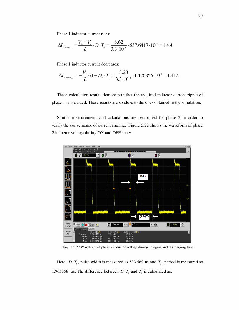
95
Phase 1 inductor current rises:
ATDL
VVI
S
oin
PhaseL4.1106417.537
103.3
62.8 9
61_,=⋅⋅
⋅=⋅⋅
−=∆ −
−
Phase 1 inductor current decreases:
ATDL
VI
S
o
PhaseL41.110426855.1
103.3
28.3)1( 6
61_,=⋅⋅
⋅=⋅−⋅−=∆ −
−
These calculation results demonstrate that the required inductor current ripple of
phase 1 is provided. These results are so close to the ones obtained in the simulation.
Similar measurements and calculations are performed for phase 2 in order to
verify the convenience of current sharing. Figure 5.22 shows the waveform of phase
2 inductor voltage during ON and OFF states.
Figure 5.22 Waveform of phase 2 inductor voltage during charging and discharging time.
Here, S
TD ⋅ , pulse width is measured as 533.569 ns and S
T , period is measured as
1.965858 µs. The difference between S
TD ⋅ and S
T is calculated as;

96
Ts – D.Ts = 1.965858 – 0.533569 = 1.432279 sµ
According to equations (3.3) and (3.4), by using the measurement results given in
Figure 5.22, inductor current ripples are calculated.
Vin =12V
Vo =3.28V
L =3.3 Hµ
D.Ts= 533.569 ns
(1-D).Ts =1.432279 sµ
Phase 2 inductor current rises:
ATDL
VVI
S
oin
PhaseL39.110569.533
103.3
62.8 9
62_,=⋅⋅
⋅=⋅⋅
−=∆ −
−
Phase 2 inductor current decreases:
ATDL
VI S
oPhaseL 42.110432279.1
103.3
28.3)1( 6
62_, =⋅⋅⋅
=⋅−⋅−=∆ −
−
In order to be sure about the accuracy of all calculations, the inductors on the
circuit are disconnected as seen in Figure 5.23 and then the inductor current ripples
are measured.
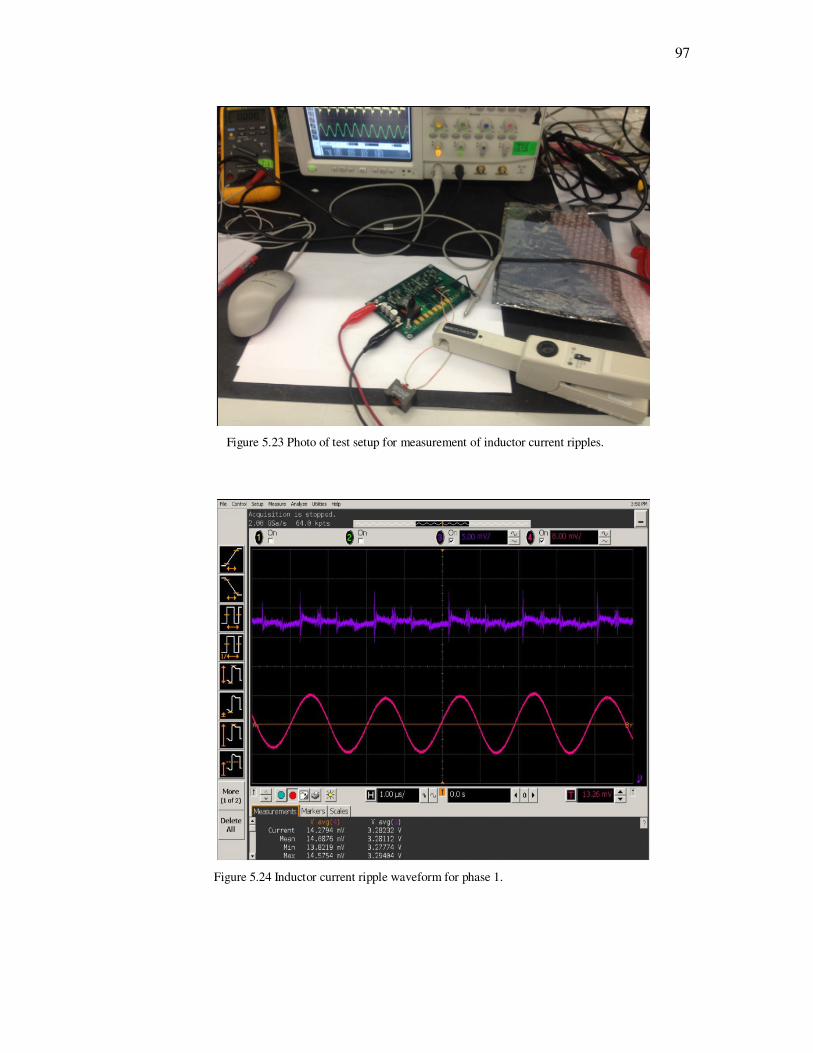
97
Figure 5.23 Photo of test setup for measurement of inductor current ripples.
Figure 5.24 Inductor current ripple waveform for phase 1.
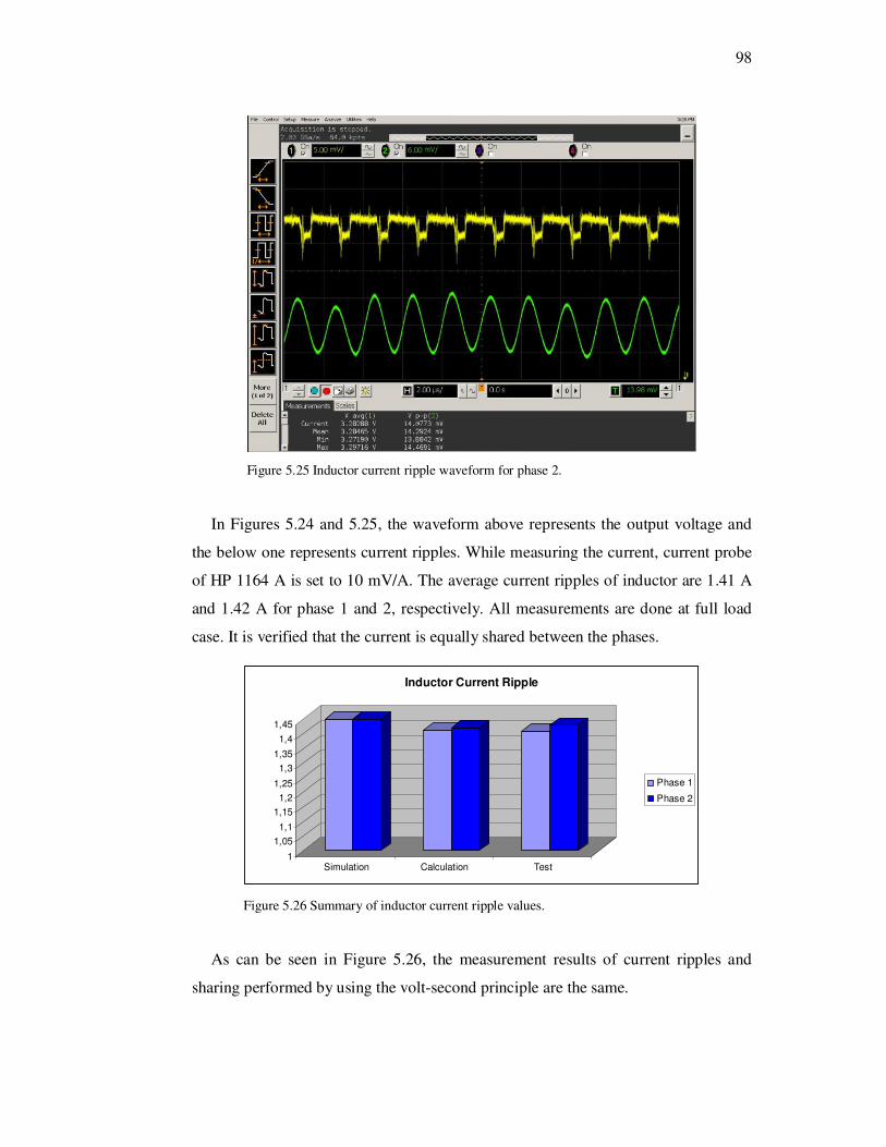
98
Figure 5.25 Inductor current ripple waveform for phase 2.
In Figures 5.24 and 5.25, the waveform above represents the output voltage and
the below one represents current ripples. While measuring the current, current probe
of HP 1164 A is set to 10 mV/A. The average current ripples of inductor are 1.41 A
and 1.42 A for phase 1 and 2, respectively. All measurements are done at full load
case. It is verified that the current is equally shared between the phases.
1
1,05
1,1
1,15
1,2
1,25
1,3
1,35
1,4
1,45
Simulation Calculation Test
Inductor Current Ripple
Phase 1
Phase 2
Figure 5.26 Summary of inductor current ripple values.
As can be seen in Figure 5.26, the measurement results of current ripples and
sharing performed by using the volt-second principle are the same.
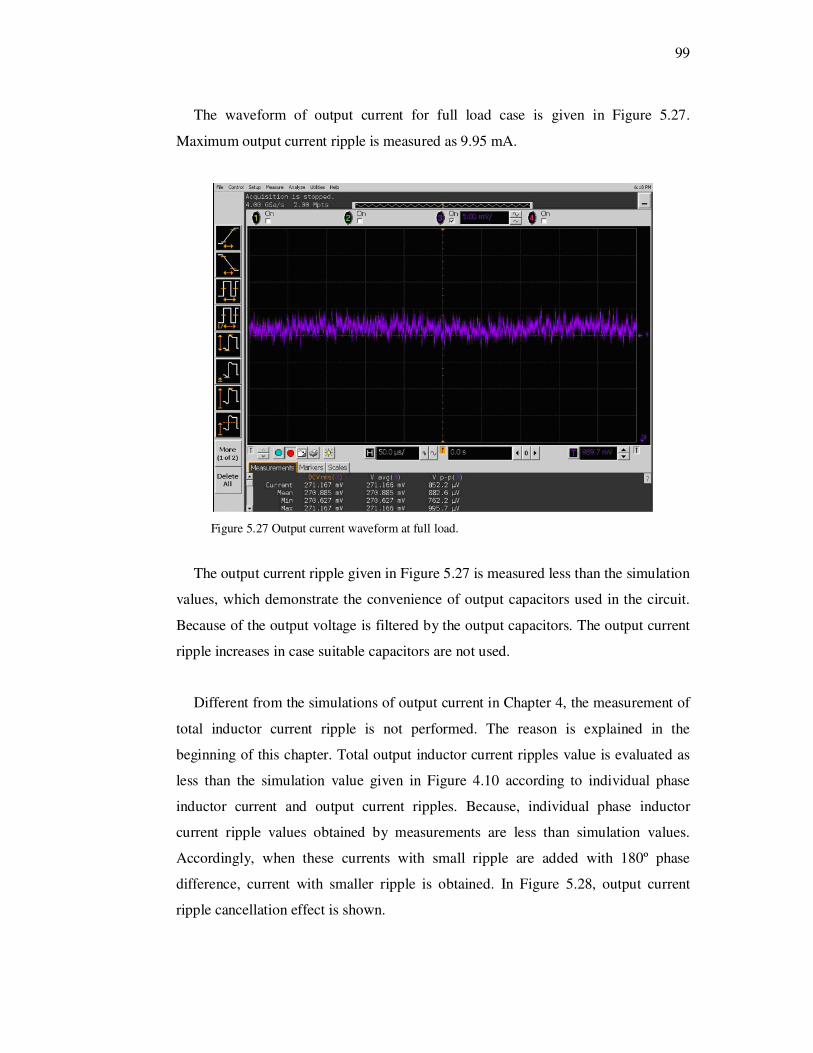
99
The waveform of output current for full load case is given in Figure 5.27.
Maximum output current ripple is measured as 9.95 mA.
Figure 5.27 Output current waveform at full load.
The output current ripple given in Figure 5.27 is measured less than the simulation
values, which demonstrate the convenience of output capacitors used in the circuit.
Because of the output voltage is filtered by the output capacitors. The output current
ripple increases in case suitable capacitors are not used.
Different from the simulations of output current in Chapter 4, the measurement of
total inductor current ripple is not performed. The reason is explained in the
beginning of this chapter. Total output inductor current ripples value is evaluated as
less than the simulation value given in Figure 4.10 according to individual phase
inductor current and output current ripples. Because, individual phase inductor
current ripple values obtained by measurements are less than simulation values.
Accordingly, when these currents with small ripple are added with 180º phase
difference, current with smaller ripple is obtained. In Figure 5.28, output current
ripple cancellation effect is shown.
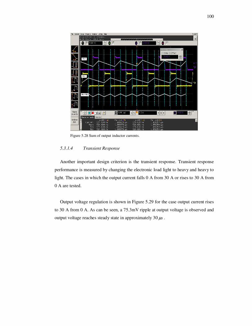
100
Figure 5.28 Sum of output inductor currents.
5.3.1.4 Transient Response
Another important design criterion is the transient response. Transient response
performance is measured by changing the electronic load light to heavy and heavy to
light. The cases in which the output current falls 0 A from 30 A or rises to 30 A from
0 A are tested.
Output voltage regulation is shown in Figure 5.29 for the case output current rises
to 30 A from 0 A. As can be seen, a 75.3mV ripple at output voltage is observed and
output voltage reaches steady state in approximately 30 sµ .
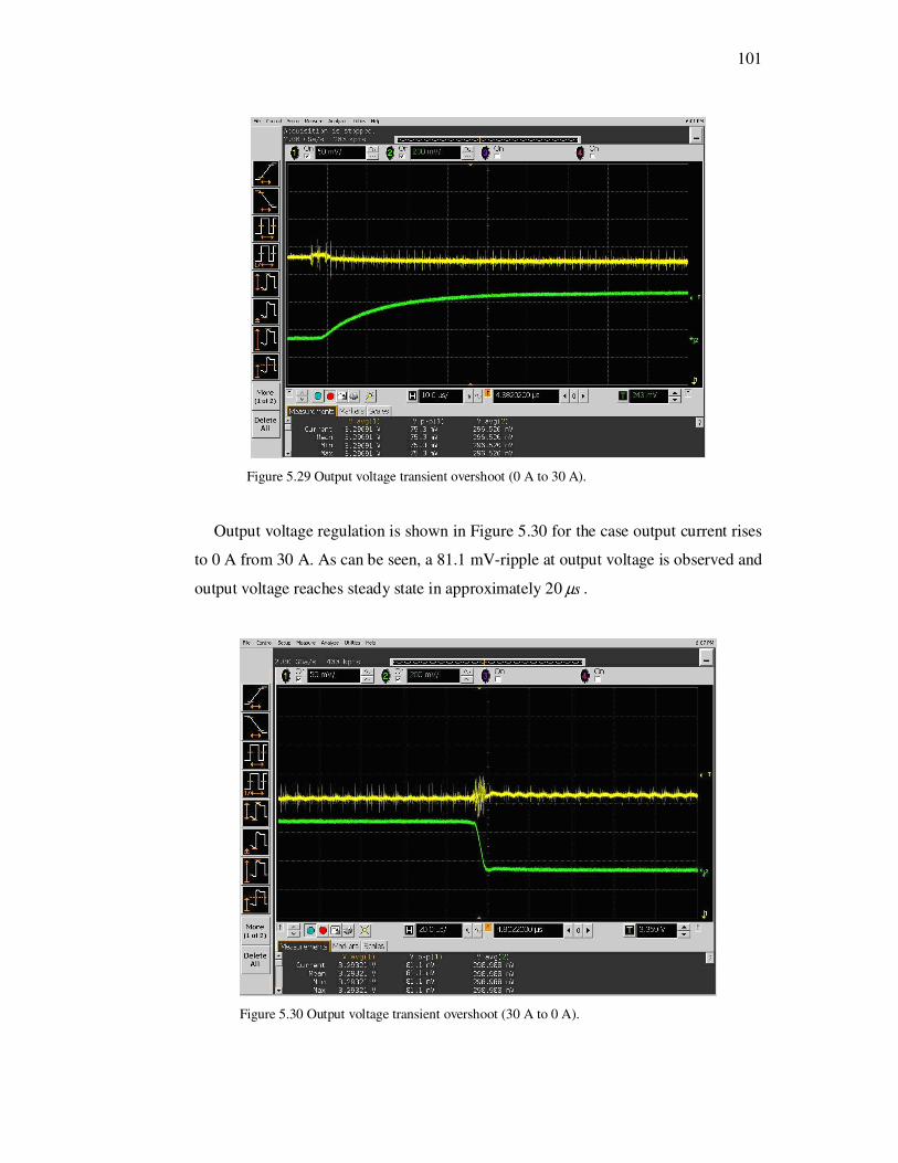
101
Figure 5.29 Output voltage transient overshoot (0 A to 30 A).
Output voltage regulation is shown in Figure 5.30 for the case output current rises
to 0 A from 30 A. As can be seen, a 81.1 mV-ripple at output voltage is observed and
output voltage reaches steady state in approximately 20 sµ .
Figure 5.30 Output voltage transient overshoot (30 A to 0 A).
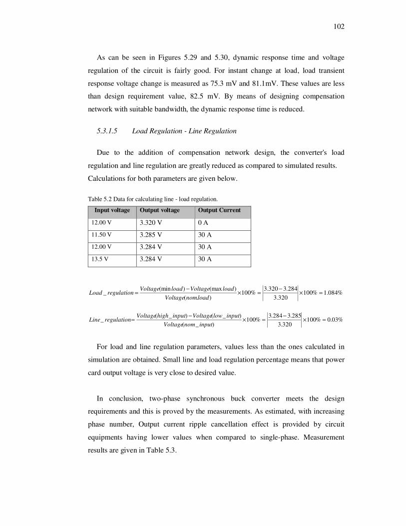
102
As can be seen in Figures 5.29 and 5.30, dynamic response time and voltage
regulation of the circuit is fairly good. For instant change at load, load transient
response voltage change is measured as 75.3 mV and 81.1mV. These values are less
than design requirement value, 82.5 mV. By means of designing compensation
network with suitable bandwidth, the dynamic response time is reduced.
5.3.1.5 Load Regulation - Line Regulation
Due to the addition of compensation network design, the converter's load
regulation and line regulation are greatly reduced as compared to simulated results.
Calculations for both parameters are given below.
Table 5.2 Data for calculating line - load regulation.
Input voltage Output voltage Output Current
12.00 V 3.320 V 0 A
11.50 V 3.285 V 30 A
12.00 V 3.284 V 30 A
13.5 V 3.284 V 30 A
%084.1%100320.3
284.3320.3%100
).(
)(max)(min_ =×
−=×
−=
loadnomVoltage
loadVoltageloadVoltageregulationLoad
%03.0%100320.3
285.3284.3%100
)_(
)_()_(_ =×
−=×
−=
inputnomVoltage
inputlowVoltageinputhighVoltageregulationLine
For load and line regulation parameters, values less than the ones calculated in
simulation are obtained. Small line and load regulation percentage means that power
card output voltage is very close to desired value.
In conclusion, two-phase synchronous buck converter meets the design
requirements and this is proved by the measurements. As estimated, with increasing
phase number, Output current ripple cancellation effect is provided by circuit
equipments having lower values when compared to single-phase. Measurement
results are given in Table 5.3.
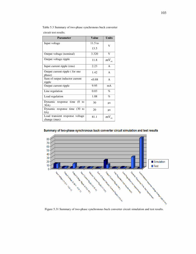
103
Table 5.3 Summary of two-phase synchronous buck converter
circuit test results.
Parameter Value Units
Input voltage 11.5 to
13.5 V
Output voltage (nominal) 3.320 V
Output voltage ripple 11.8 PK
mV
Input current ripple (rms) 2.23 A
Output current ripple ( for one phase)
1.42 A
Sum of output inductor current ripple
<0.88 A
Output current ripple 9.95 mA
Line regulation 0.03 %
Load regulation 1.08 %
Dynamic response time (0 to 30A)
30 µs
Dynamic response time (30 to 0A)
20 µs
Load transient response voltage change (max)
81.1 PK
mV
Figure 5.31 Summary of two-phase synchronous buck converter circuit simulation and test results.
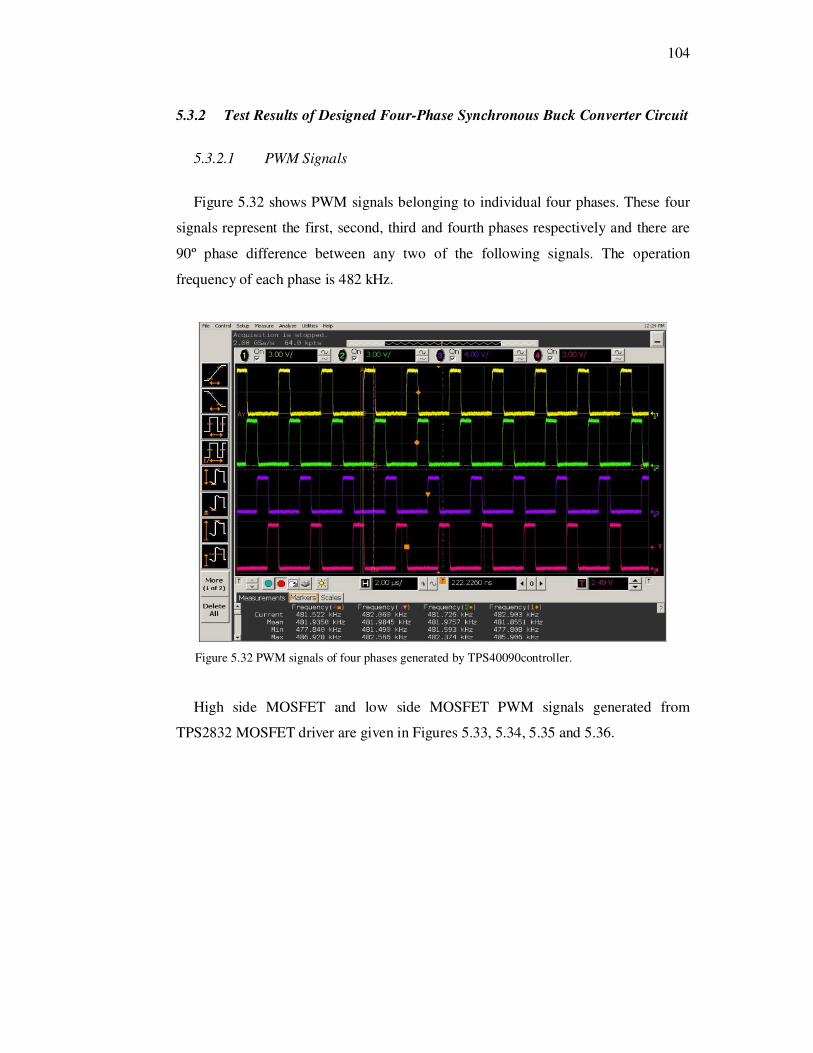
104
5.3.2 Test Results of Designed Four-Phase Synchronous Buck Converter Circuit
5.3.2.1 PWM Signals
Figure 5.32 shows PWM signals belonging to individual four phases. These four
signals represent the first, second, third and fourth phases respectively and there are
90º phase difference between any two of the following signals. The operation
frequency of each phase is 482 kHz.
Figure 5.32 PWM signals of four phases generated by TPS40090controller.
High side MOSFET and low side MOSFET PWM signals generated from
TPS2832 MOSFET driver are given in Figures 5.33, 5.34, 5.35 and 5.36.
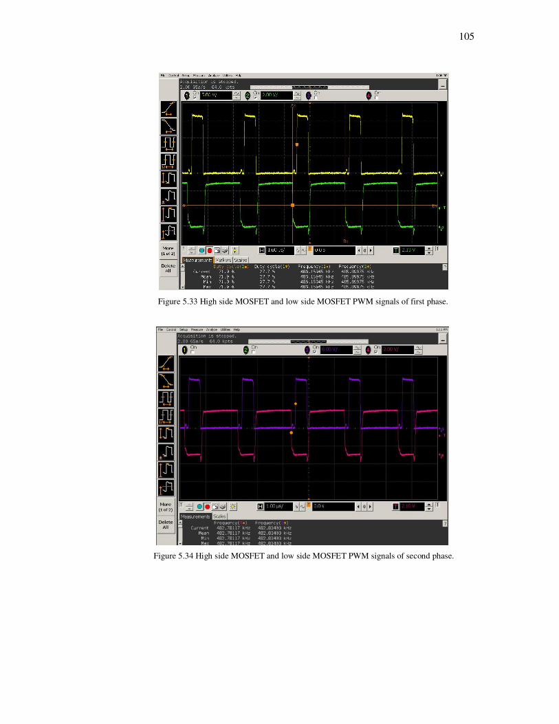
105
Figure 5.33 High side MOSFET and low side MOSFET PWM signals of first phase.
Figure 5.34 High side MOSFET and low side MOSFET PWM signals of second phase.
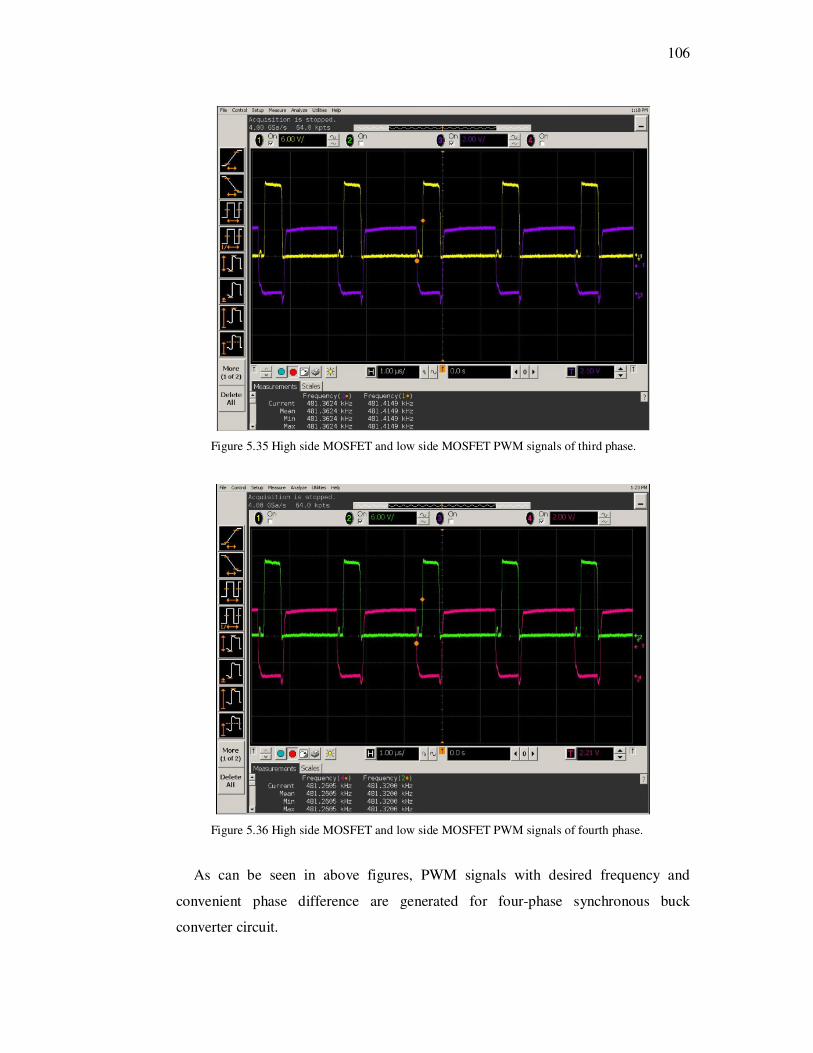
106
Figure 5.35 High side MOSFET and low side MOSFET PWM signals of third phase.
Figure 5.36 High side MOSFET and low side MOSFET PWM signals of fourth phase.
As can be seen in above figures, PWM signals with desired frequency and
convenient phase difference are generated for four-phase synchronous buck
converter circuit.
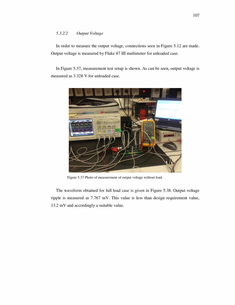
107
5.3.2.2 Output Voltage
In order to measure the output voltage, connections seen in Figure 5.12 are made.
Output voltage is measured by Fluke 87 III multimeter for unloaded case.
In Figure 5.37, measurement test setup is shown. As can be seen, output voltage is
measured as 3.328 V for unloaded case.
Figure 5.37 Photo of measurement of output voltage without load.
The waveform obtained for full load case is given in Figure 5.38. Output voltage
ripple is measured as 7.767 mV. This value is less than design requirement value,
13.2 mV and accordingly a suitable value.
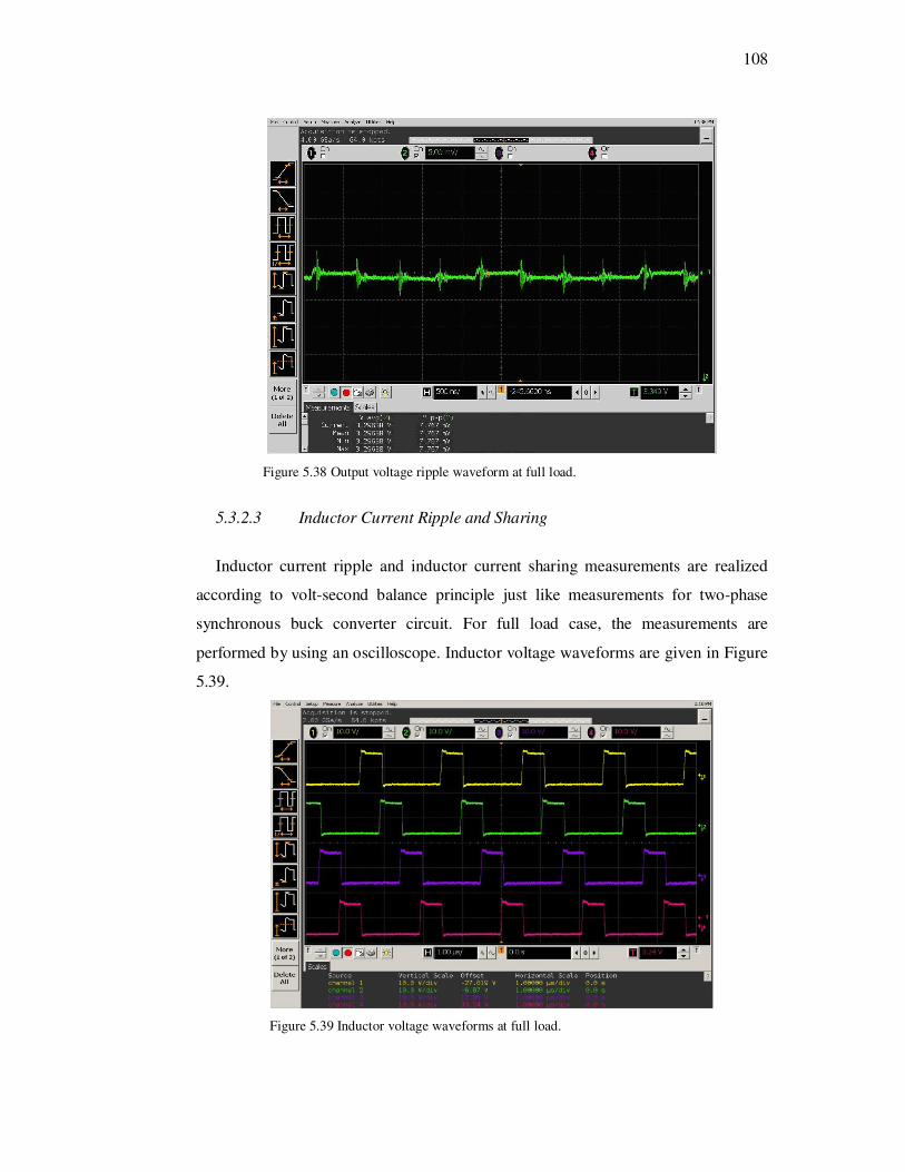
108
Figure 5.38 Output voltage ripple waveform at full load.
5.3.2.3 Inductor Current Ripple and Sharing
Inductor current ripple and inductor current sharing measurements are realized
according to volt-second balance principle just like measurements for two-phase
synchronous buck converter circuit. For full load case, the measurements are
performed by using an oscilloscope. Inductor voltage waveforms are given in Figure
5.39.
Figure 5.39 Inductor voltage waveforms at full load.
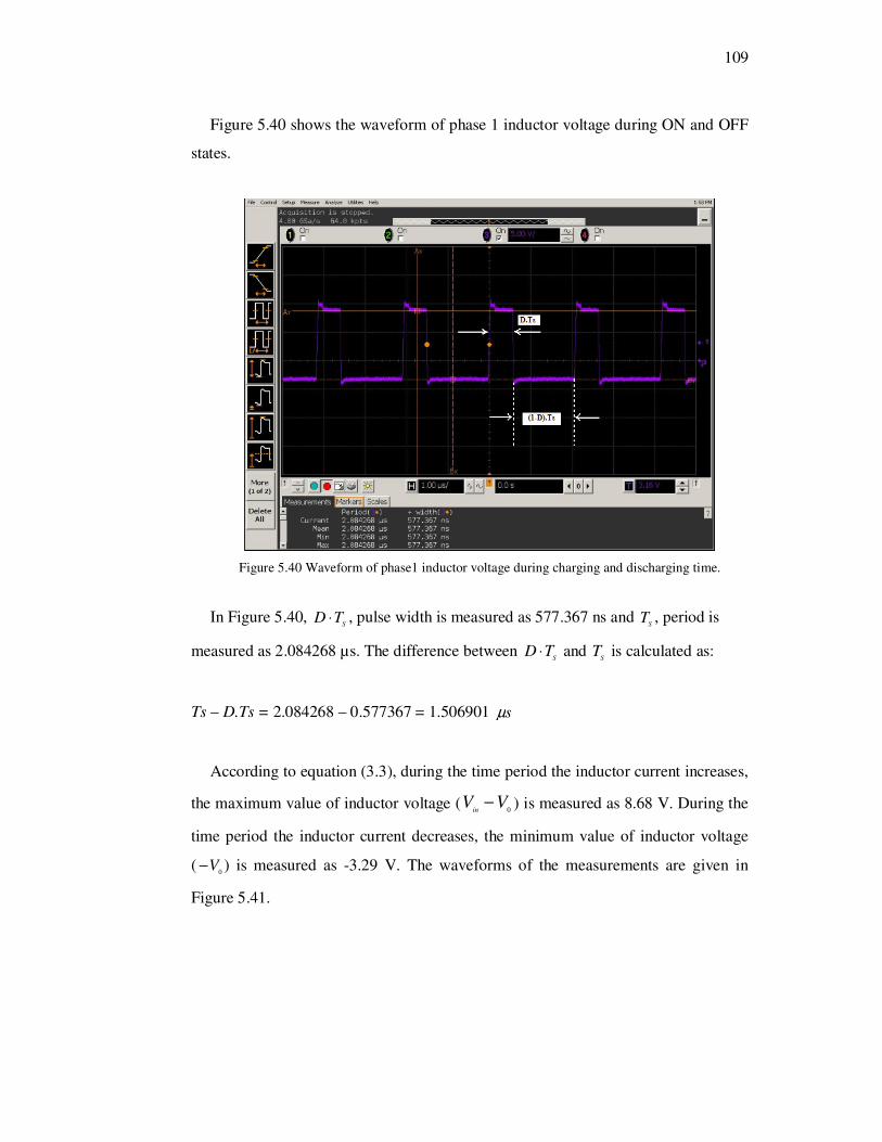
109
Figure 5.40 shows the waveform of phase 1 inductor voltage during ON and OFF
states.
Figure 5.40 Waveform of phase1 inductor voltage during charging and discharging time.
In Figure 5.40, S
TD ⋅ , pulse width is measured as 577.367 ns and S
T , period is
measured as 2.084268 µs. The difference between S
TD ⋅ and S
T is calculated as:
Ts – D.Ts = 2.084268 – 0.577367 = 1.506901 sµ
According to equation (3.3), during the time period the inductor current increases,
the maximum value of inductor voltage ( 0VV
in− ) is measured as 8.68 V. During the
time period the inductor current decreases, the minimum value of inductor voltage
(0
V− ) is measured as -3.29 V. The waveforms of the measurements are given in
Figure 5.41.
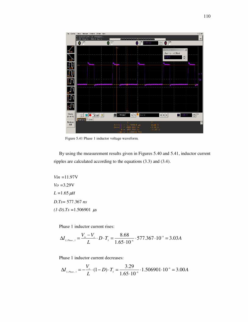
110
Figure 5.41 Phase 1 inductor voltage waveform.
By using the measurement results given in Figures 5.40 and 5.41, inductor current
ripples are calculated according to the equations (3.3) and (3.4).
Vin =11.97V
Vo =3.29V
L =1.65 Hµ
D.Ts= 577.367 ns
(1-D).Ts =1.506901 sµ
Phase 1 inductor current rises:
ATDL
VVI
S
oin
PhaseL03.310367.577
1065.1
68.8 9
61_,=⋅⋅
⋅=⋅⋅
−=∆ −
−
Phase 1 inductor current decreases:
ATDL
VI
S
o
PhaseL00.310506901.1
1065.1
29.3)1( 6
61_,=⋅⋅
⋅=⋅−⋅−=∆ −
−
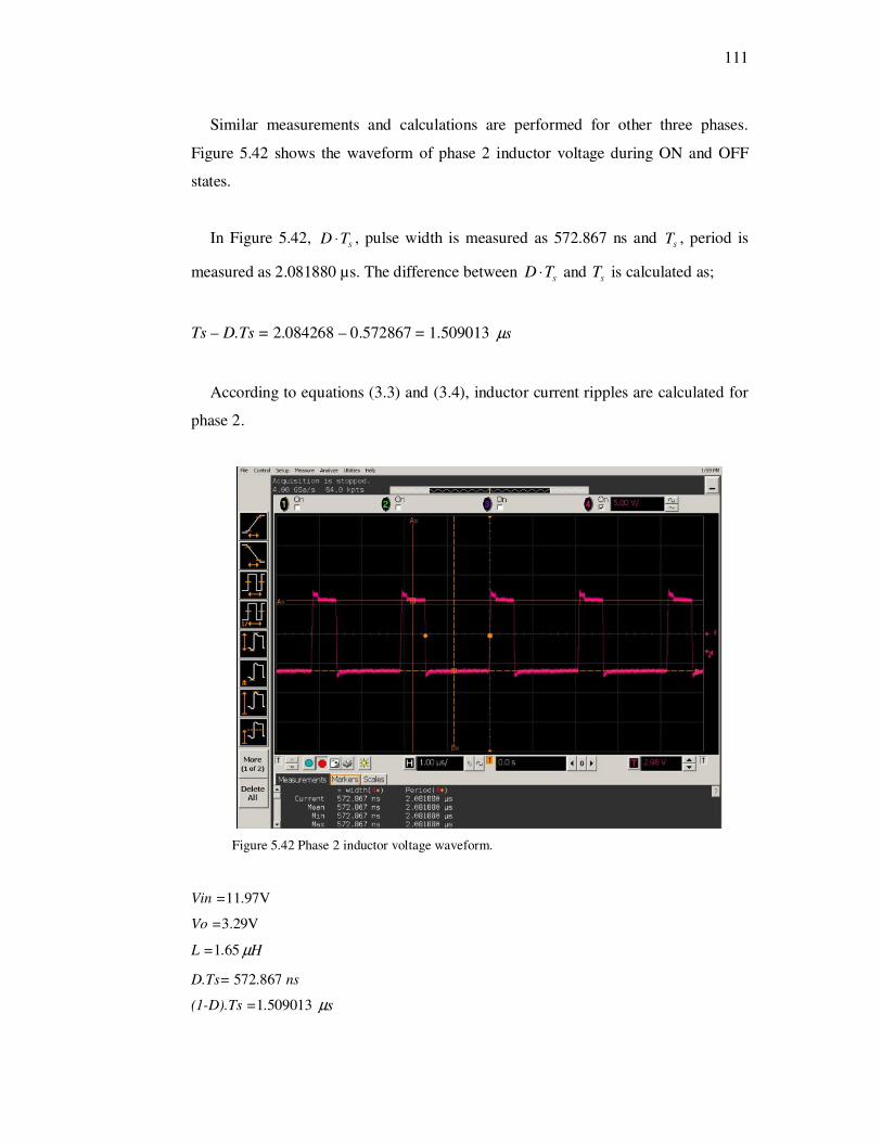
111
Similar measurements and calculations are performed for other three phases.
Figure 5.42 shows the waveform of phase 2 inductor voltage during ON and OFF
states.
In Figure 5.42, S
TD ⋅ , pulse width is measured as 572.867 ns and S
T , period is
measured as 2.081880 µs. The difference between S
TD ⋅ and S
T is calculated as;
Ts – D.Ts = 2.084268 – 0.572867 = 1.509013 sµ
According to equations (3.3) and (3.4), inductor current ripples are calculated for
phase 2.
Figure 5.42 Phase 2 inductor voltage waveform.
Vin =11.97V
Vo =3.29V
L =1.65 Hµ
D.Ts= 572.867 ns
(1-D).Ts =1.509013 sµ
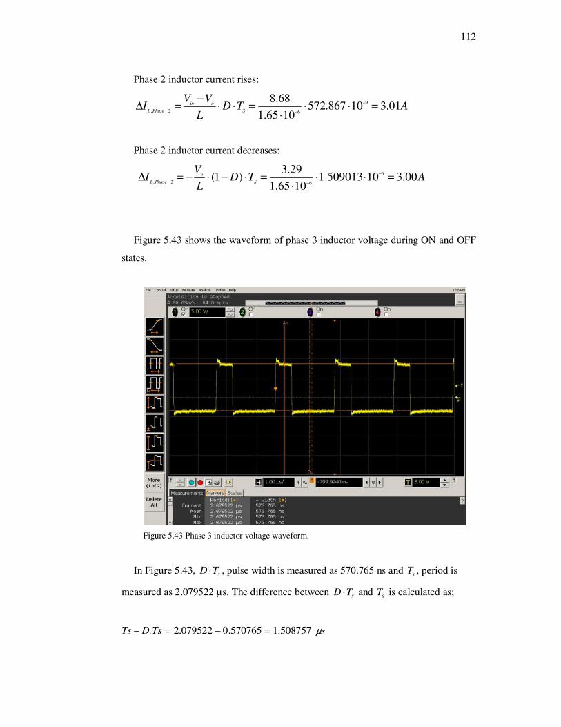
112
Phase 2 inductor current rises:
ATDL
VVI
S
oin
PhaseL01.310867.572
1065.1
68.8 9
62_,=⋅⋅
⋅=⋅⋅
−=∆ −
−
Phase 2 inductor current decreases:
ATDL
VI
S
o
PhaseL00.310509013.1
1065.1
29.3)1( 6
62_,=⋅⋅
⋅=⋅−⋅−=∆ −
−
Figure 5.43 shows the waveform of phase 3 inductor voltage during ON and OFF
states.
Figure 5.43 Phase 3 inductor voltage waveform.
In Figure 5.43, S
TD ⋅ , pulse width is measured as 570.765 ns and S
T , period is
measured as 2.079522 µs. The difference between S
TD ⋅ and S
T is calculated as;
Ts – D.Ts = 2.079522 – 0.570765 = 1.508757 sµ
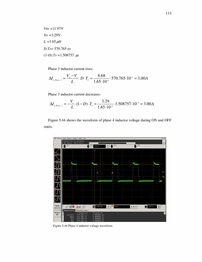
113
Vin =11.97V
Vo =3.29V
L =1.65 Hµ
D.Ts= 570.765 ns
(1-D).Ts =1.508757 sµ
Phase 3 inductor current rises:
ATDL
VVI
S
oin
PhaseL00.310765.570
1065.1
68.8 9
63_,=⋅⋅
⋅=⋅⋅
−=∆ −
−
Phase 3 inductor current decreases:
ATDL
VI
S
o
PhaseL00.310508757.1
1065.1
29.3)1( 6
63_,=⋅⋅
⋅=⋅−⋅−=∆ −
−
Figure 5.44 shows the waveform of phase 4 inductor voltage during ON and OFF
states.
Figure 5.44 Phase 4 inductor voltage waveform.
114
In Figure 5.44, S
TD ⋅ , pulse width is measured as 575.042 ns and S
T , period is
measured as 2.083940 µs. The difference between S
TD ⋅ and S
T is calculated as;
Ts – D.Ts = 2.083940 – 0.575042 = 1.508898 sµ
Vin =11.97V
Vo =3.29V
L =1.65 Hµ
D.Ts= 575.042 ns
(1-D).Ts =1.508898 sµ
Phase 4 inductor current rises:
ATDL
VVI
S
oin
PhaseL02.310042.575
1065.1
68.8 9
64_,=⋅⋅
⋅=⋅⋅
−=∆ −
−
Phase 4 inductor current decreases:
ATDL
VI
S
o
PhaseL00.310508898.1
1065.1
29.3)1( 6
64_,=⋅⋅
⋅=⋅−⋅−=∆ −
−
Calculation results show that inductor current ripples for all phases meet the
design requirement. Calculated values are so close to the values obtained in
simulation.
1
1,5
2
2,5
3
3,5
Phase 1 Phase 2 Phase 3 Phase 4
Inductor Current Ripple
Simulation
Test
Figure 5.45 Summary of inductor current ripple values.
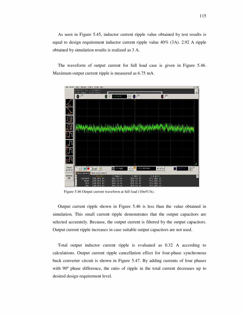
115
As seen in Figure 5.45, inductor current ripple value obtained by test results is
equal to design requirement inductor current ripple value 40% (3A). 2.92 A ripple
obtained by simulation results is realized as 3 A.
The waveform of output current for full load case is given in Figure 5.46.
Maximum output current ripple is measured as 6.75 mA.
Figure 5.46 Output current waveform at full load (10mV/A).
Output current ripple shown in Figure 5.46 is less than the value obtained in
simulation. This small current ripple demonstrates that the output capacitors are
selected accurately. Because, the output current is filtered by the output capacitors.
Output current ripple increases in case suitable output capacitors are not used.
Total output inductor current ripple is evaluated as 0.32 A according to
calculations. Output current ripple cancellation effect for four-phase synchronous
buck converter circuit is shown in Figure 5.47. By adding currents of four phases
with 90º phase difference, the ratio of ripple in the total current decreases up to
desired design requirement level.
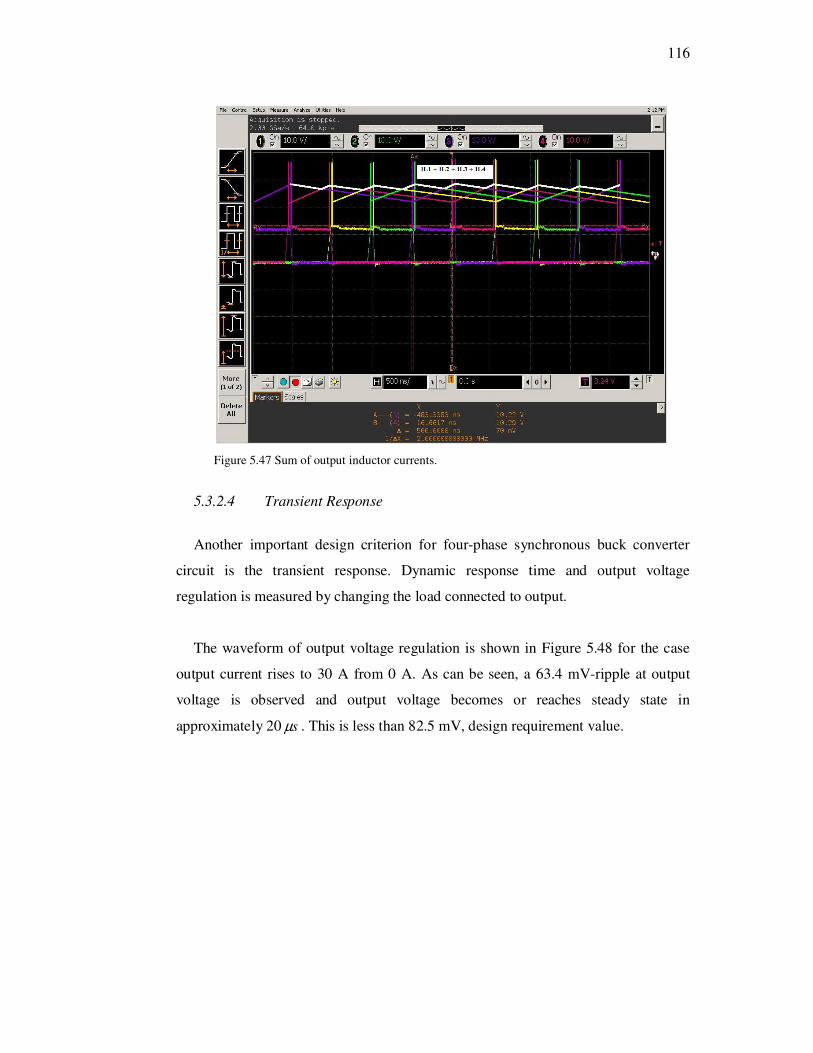
116
Figure 5.47 Sum of output inductor currents.
5.3.2.4 Transient Response
Another important design criterion for four-phase synchronous buck converter
circuit is the transient response. Dynamic response time and output voltage
regulation is measured by changing the load connected to output.
The waveform of output voltage regulation is shown in Figure 5.48 for the case
output current rises to 30 A from 0 A. As can be seen, a 63.4 mV-ripple at output
voltage is observed and output voltage becomes or reaches steady state in
approximately 20 sµ . This is less than 82.5 mV, design requirement value.
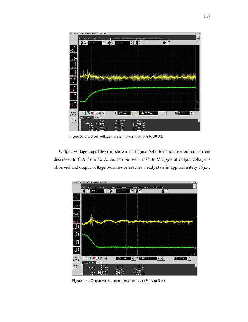
117
Figure 5.48 Output voltage transient overshoot (0 A to 30 A).
Output voltage regulation is shown in Figure 5.49 for the case output current
decreases to 0 A from 30 A. As can be seen, a 75.3mV ripple at output voltage is
observed and output voltage becomes or reaches steady state in approximately 15 sµ .
Figure 5.49 Output voltage transient overshoot (30 A to 0 A).
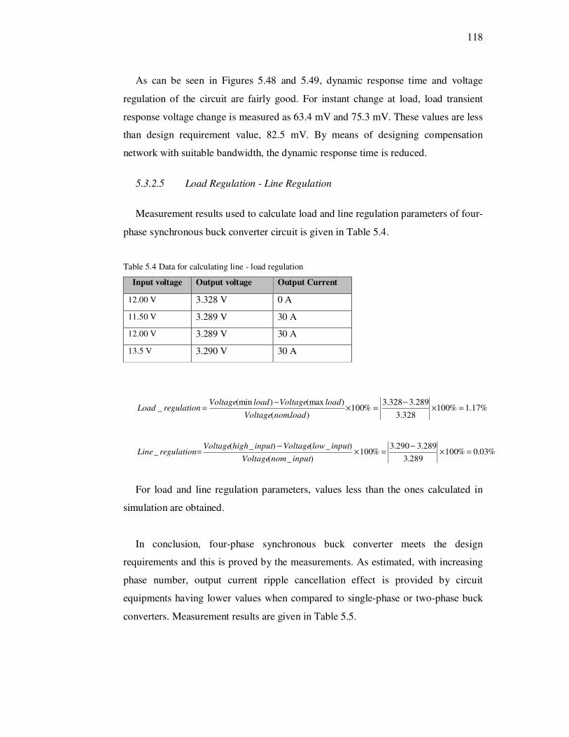
118
As can be seen in Figures 5.48 and 5.49, dynamic response time and voltage
regulation of the circuit are fairly good. For instant change at load, load transient
response voltage change is measured as 63.4 mV and 75.3 mV. These values are less
than design requirement value, 82.5 mV. By means of designing compensation
network with suitable bandwidth, the dynamic response time is reduced.
5.3.2.5 Load Regulation - Line Regulation
Measurement results used to calculate load and line regulation parameters of four-
phase synchronous buck converter circuit is given in Table 5.4.
Table 5.4 Data for calculating line - load regulation
Input voltage Output voltage Output Current
12.00 V 3.328 V 0 A
11.50 V 3.289 V 30 A
12.00 V 3.289 V 30 A
13.5 V 3.290 V 30 A
%17.1%100328.3
289.3328.3%100
).(
)(max)(min_ =×
−=×
−=
loadnomVoltage
loadVoltageloadVoltageregulationLoad
%03.0%100289.3
289.3290.3%100
)_(
)_()_(_ =×
−=×
−=
inputnomVoltage
inputlowVoltageinputhighVoltageregulationLine
For load and line regulation parameters, values less than the ones calculated in
simulation are obtained.
In conclusion, four-phase synchronous buck converter meets the design
requirements and this is proved by the measurements. As estimated, with increasing
phase number, output current ripple cancellation effect is provided by circuit
equipments having lower values when compared to single-phase or two-phase buck
converters. Measurement results are given in Table 5.5.
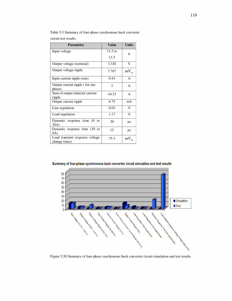
119
Table 5.5 Summary of four-phase synchronous buck converter
circuit test results.
Parameter Value Units
Input voltage 11.5 to
13.5 V
Output voltage (nominal) 3.328 V
Output voltage ripple 7.767 PK
mV
Input current ripple (rms) 0.43 A
Output current ripple ( for one phase)
3 A
Sum of output inductor current ripple
<0.33 A
Output current ripple 6.75 mA
Line regulation 0.03 %
Load regulation 1.17 %
Dynamic response time (0 to 30A)
20 µs
Dynamic response time (30 to 0A)
15 µs
Load transient response voltage change (max)
75.3 PK
mV
Figure 5.50 Summary of four-phase synchronous buck converter circuit simulation and test results.
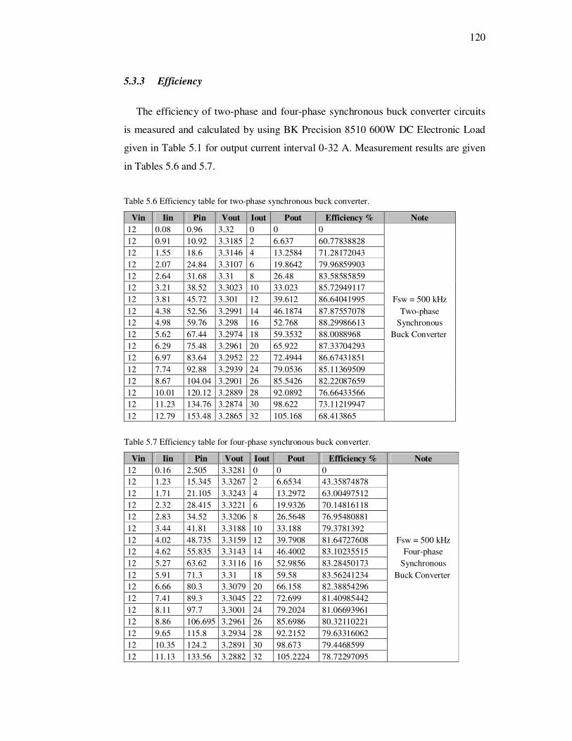
120
5.3.3 Efficiency
The efficiency of two-phase and four-phase synchronous buck converter circuits
is measured and calculated by using BK Precision 8510 600W DC Electronic Load
given in Table 5.1 for output current interval 0-32 A. Measurement results are given
in Tables 5.6 and 5.7.
Table 5.6 Efficiency table for two-phase synchronous buck converter.
Vin Iin Pin Vout Iout Pout Efficiency % Note 12 0.08 0.96 3.32 0 0 0
12 0.91 10.92 3.3185 2 6.637 60.77838828
12 1.55 18.6 3.3146 4 13.2584 71.28172043
12 2.07 24.84 3.3107 6 19.8642 79.96859903
12 2.64 31.68 3.31 8 26.48 83.58585859 12 3.21 38.52 3.3023 10 33.023 85.72949117
12 3.81 45.72 3.301 12 39.612 86.64041995 Fsw = 500 kHz
12 4.38 52.56 3.2991 14 46.1874 87.87557078 Two-phase 12 4.98 59.76 3.298 16 52.768 88.29986613 Synchronous
12 5.62 67.44 3.2974 18 59.3532 88.0088968 Buck Converter
12 6.29 75.48 3.2961 20 65.922 87.33704293
12 6.97 83.64 3.2952 22 72.4944 86.67431851
12 7.74 92.88 3.2939 24 79.0536 85.11369509
12 8.67 104.04 3.2901 26 85.5426 82.22087659
12 10.01 120.12 3.2889 28 92.0892 76.66433566 12 11.23 134.76 3.2874 30 98.622 73.11219947
12 12.79 153.48 3.2865 32 105.168 68.413865
Table 5.7 Efficiency table for four-phase synchronous buck converter.
Vin Iin Pin Vout Iout Pout Efficiency % Note 12 0.16 2.505 3.3281 0 0 0 12 1.23 15.345 3.3267 2 6.6534 43.35874878
12 1.71 21.105 3.3243 4 13.2972 63.00497512
12 2.32 28.415 3.3221 6 19.9326 70.14816118
12 2.83 34.52 3.3206 8 26.5648 76.95480881
12 3.44 41.81 3.3188 10 33.188 79.3781392
12 4.02 48.735 3.3159 12 39.7908 81.64727608 Fsw = 500 kHz 12 4.62 55.835 3.3143 14 46.4002 83.10235515 Four-phase
12 5.27 63.62 3.3116 16 52.9856 83.28450173 Synchronous
12 5.91 71.3 3.31 18 59.58 83.56241234 Buck Converter 12 6.66 80.3 3.3079 20 66.158 82.38854296
12 7.41 89.3 3.3045 22 72.699 81.40985442
12 8.11 97.7 3.3001 24 79.2024 81.06693961
12 8.86 106.695 3.2961 26 85.6986 80.32110221
12 9.65 115.8 3.2934 28 92.2152 79.63316062
12 10.35 124.2 3.2891 30 98.673 79.4468599
12 11.13 133.56 3.2882 32 105.2224 78.72297095
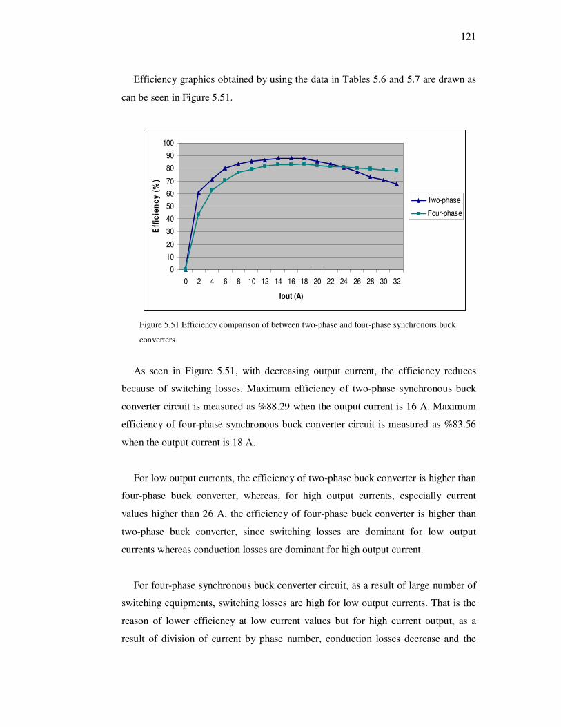
121
Efficiency graphics obtained by using the data in Tables 5.6 and 5.7 are drawn as
can be seen in Figure 5.51.
0
10
20
30
40
50
60
70
80
90
100
0 2 4 6 8 10 12 14 16 18 20 22 24 26 28 30 32
Iout (A)
Eff
icie
nc
y (
%)
Two-phase
Four-phase
Figure 5.51 Efficiency comparison of between two-phase and four-phase synchronous buck
converters.
As seen in Figure 5.51, with decreasing output current, the efficiency reduces
because of switching losses. Maximum efficiency of two-phase synchronous buck
converter circuit is measured as %88.29 when the output current is 16 A. Maximum
efficiency of four-phase synchronous buck converter circuit is measured as %83.56
when the output current is 18 A.
For low output currents, the efficiency of two-phase buck converter is higher than
four-phase buck converter, whereas, for high output currents, especially current
values higher than 26 A, the efficiency of four-phase buck converter is higher than
two-phase buck converter, since switching losses are dominant for low output
currents whereas conduction losses are dominant for high output current.
For four-phase synchronous buck converter circuit, as a result of large number of
switching equipments, switching losses are high for low output currents. That is the
reason of lower efficiency at low current values but for high current output, as a
result of division of current by phase number, conduction losses decrease and the

122
efficiency becomes higher than the efficiency of two-phase synchronous buck
converter.
In conclusion, with increasing phase number, the efficiency becomes higher for
high output currents.
5.3.4 Electromagnetic Compatibility (EMC) Tests
Delaballe (2001) defines Electromagnetic Compatibility as “The ability of an
equipment or system to function satisfactorily in its electromagnetic environment
without introducing intolerable electromagnetic disturbances to anything in that
environment” (Delaballe, 2001, p.2).
Electromagnetic compatibility tests are frequently realized in commercial
applications nowadays. Televisions, mobile phones, devices used in military field are
tested according to certain standards.
There are 4 main kinds of compatibility tests as;
CE - Conducted Emission
CS - Conducted Susceptibility
RE - Radiated Emission
RS - Radiated Susceptibility
CE101 and CE102 tests of designed two-phase and four-phase synchronous buck
converter circuits are realized according to MIL-STD-461E military standard
(Department of Defense USA, 1999).
5.3.4.1 CE101 Test (30 Hz – 10 kHz)
The aim of the test is to measure conducted emission level of designed two-phase
and four-phase buck converter circuits to external environment for frequency interval
30 Hz – 10 kHz.
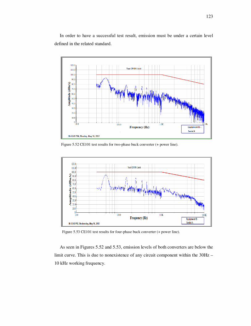
123
In order to have a successful test result, emission must be under a certain level
defined in the related standard.
Figure 5.52 CE101 test results for two-phase buck converter (+ power line).
Figure 5.53 CE101 test results for four-phase buck converter (+ power line).
As seen in Figures 5.52 and 5.53, emission levels of both converters are below the
limit curve. This is due to nonexistence of any circuit component within the 30Hz –
10 kHz working frequency.
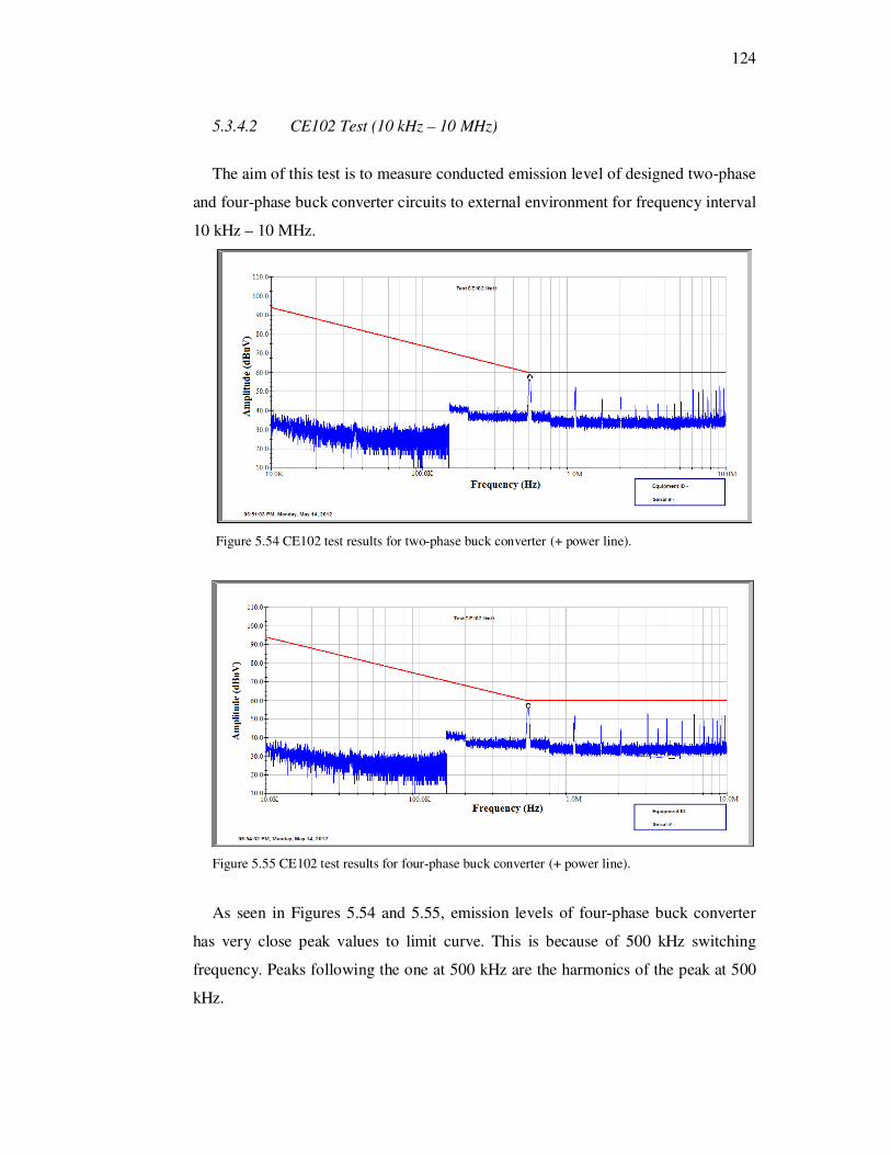
124
5.3.4.2 CE102 Test (10 kHz – 10 MHz)
The aim of this test is to measure conducted emission level of designed two-phase
and four-phase buck converter circuits to external environment for frequency interval
10 kHz – 10 MHz.
Figure 5.54 CE102 test results for two-phase buck converter (+ power line).
Figure 5.55 CE102 test results for four-phase buck converter (+ power line).
As seen in Figures 5.54 and 5.55, emission levels of four-phase buck converter
has very close peak values to limit curve. This is because of 500 kHz switching
frequency. Peaks following the one at 500 kHz are the harmonics of the peak at 500
kHz.
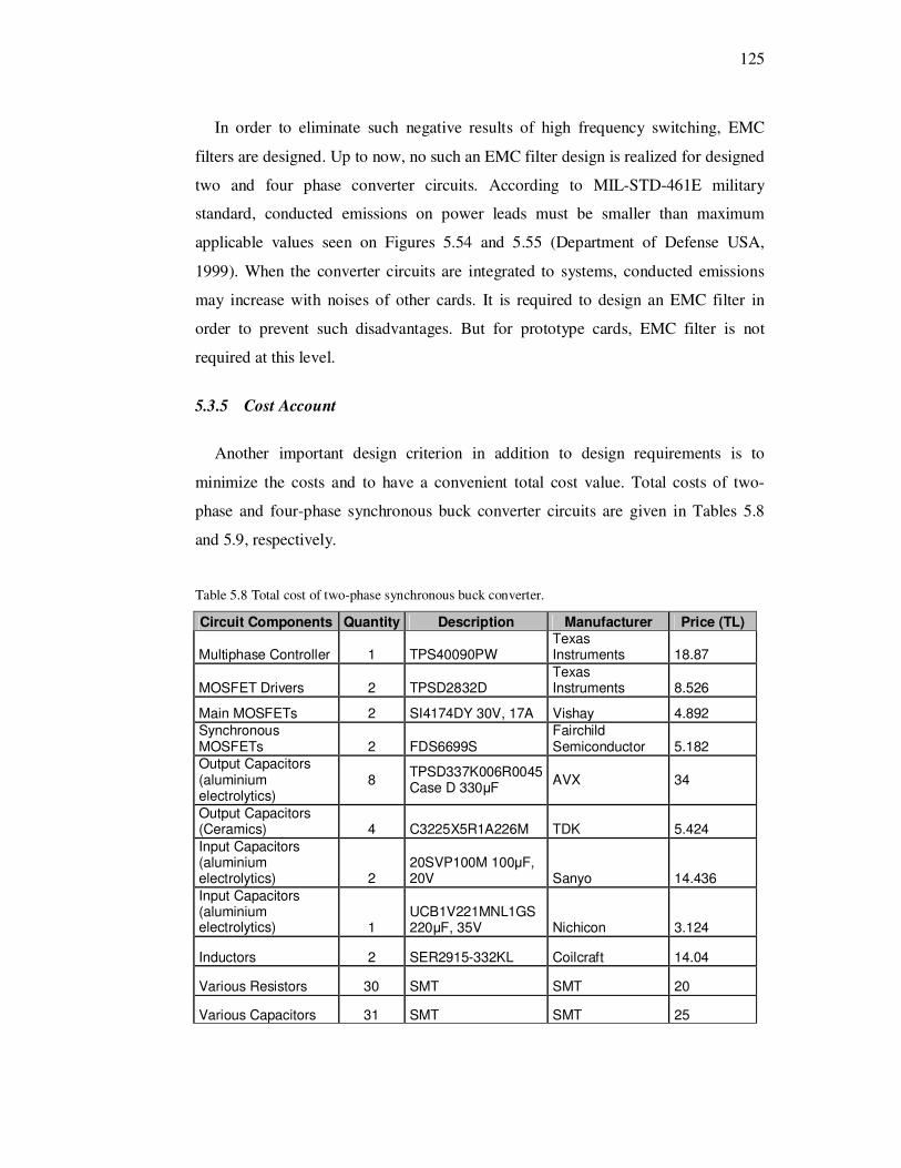
125
In order to eliminate such negative results of high frequency switching, EMC
filters are designed. Up to now, no such an EMC filter design is realized for designed
two and four phase converter circuits. According to MIL-STD-461E military
standard, conducted emissions on power leads must be smaller than maximum
applicable values seen on Figures 5.54 and 5.55 (Department of Defense USA,
1999). When the converter circuits are integrated to systems, conducted emissions
may increase with noises of other cards. It is required to design an EMC filter in
order to prevent such disadvantages. But for prototype cards, EMC filter is not
required at this level.
5.3.5 Cost Account
Another important design criterion in addition to design requirements is to
minimize the costs and to have a convenient total cost value. Total costs of two-
phase and four-phase synchronous buck converter circuits are given in Tables 5.8
and 5.9, respectively.
Table 5.8 Total cost of two-phase synchronous buck converter.
Circuit Components Quantity Description Manufacturer Price (TL)
Multiphase Controller 1 TPS40090PW Texas Instruments 18.87
MOSFET Drivers 2 TPSD2832D Texas Instruments 8.526
Main MOSFETs 2 SI4174DY 30V, 17A Vishay 4.892
Synchronous MOSFETs 2 FDS6699S
Fairchild Semiconductor 5.182
Output Capacitors (aluminium electrolytics)
8 TPSD337K006R0045 Case D 330µF
AVX 34
Output Capacitors (Ceramics) 4 C3225X5R1A226M TDK 5.424
Input Capacitors (aluminium electrolytics) 2
20SVP100M 100µF, 20V Sanyo 14.436
Input Capacitors (aluminium electrolytics) 1
UCB1V221MNL1GS 220µF, 35V Nichicon 3.124
Inductors 2 SER2915-332KL Coilcraft 14.04
Various Resistors 30 SMT SMT 20
Various Capacitors 31 SMT SMT 25
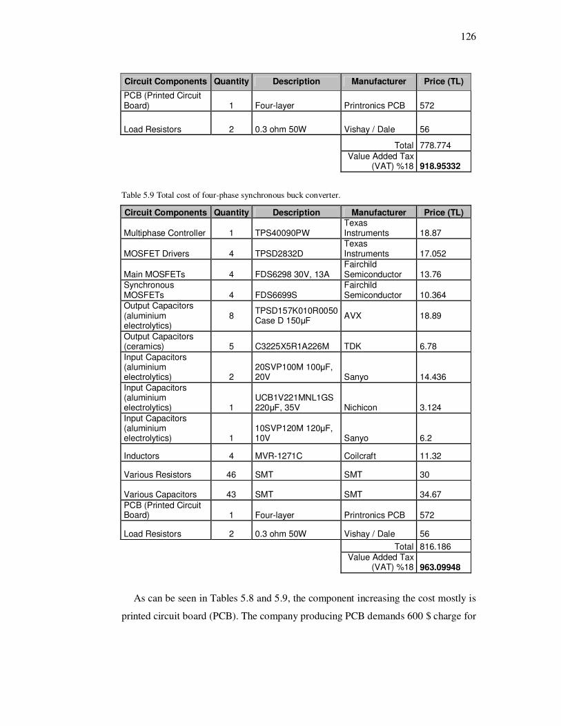
126
Circuit Components Quantity Description Manufacturer Price (TL)
PCB (Printed Circuit Board) 1 Four-layer Printronics PCB 572
Load Resistors 2 0.3 ohm 50W Vishay / Dale 56
Total 778.774
Value Added Tax
(VAT) %18 918.95332
Table 5.9 Total cost of four-phase synchronous buck converter.
Circuit Components Quantity Description Manufacturer Price (TL)
Multiphase Controller 1 TPS40090PW Texas Instruments 18.87
MOSFET Drivers 4 TPSD2832D Texas Instruments 17.052
Main MOSFETs 4 FDS6298 30V, 13A Fairchild Semiconductor 13.76
Synchronous MOSFETs 4 FDS6699S
Fairchild Semiconductor 10.364
Output Capacitors (aluminium electrolytics)
8 TPSD157K010R0050 Case D 150µF
AVX 18.89
Output Capacitors (ceramics) 5 C3225X5R1A226M TDK 6.78
Input Capacitors (aluminium electrolytics) 2
20SVP100M 100µF, 20V Sanyo 14.436
Input Capacitors (aluminium electrolytics) 1
UCB1V221MNL1GS 220µF, 35V Nichicon 3.124
Input Capacitors (aluminium electrolytics) 1
10SVP120M 120µF, 10V Sanyo 6.2
Inductors 4 MVR-1271C Coilcraft 11.32
Various Resistors 46 SMT SMT 30
Various Capacitors 43 SMT SMT 34.67
PCB (Printed Circuit Board) 1 Four-layer Printronics PCB 572
Load Resistors 2 0.3 ohm 50W Vishay / Dale 56
Total 816.186
Value Added Tax
(VAT) %18 963.09948
As can be seen in Tables 5.8 and 5.9, the component increasing the cost mostly is
printed circuit board (PCB). The company producing PCB demands 600 $ charge for

127
setup tooling of two cards. But after this first production, only 5 $ is charged for each
PCB production, meaning a quite decrease at costs for duplicate production process.
The number of used high side (main) MOSFET, low side (synchronous) MOSFET
and MOSFET driver integrated circuit proportionally increases with the increase of
phase number of multiphase architecture. But, with increasing phase number, the
inductance value and accordingly output capacitor value decreases. Thus, circuit
components with smaller values are used. This is even the number of MOSFET and
MOSFET driver increases, the cost is balanced by using output capacitors with lower
values and inductors with lower current. Even the number of phase increase, the total
amount of cost does not increase suddenly.
Total costs of two-phase synchronous buck converter
73%
0%
2%
3%
3%
2%1%
4%1%
1%1%
2%
7%Multiphase Controller
MOSFET Driver
Main MOSFET
Synchronous MOSFET
Output Capacitors (aluminium electrolytics)
Output Capacitors (Ceramics)
Input Capacitors (aluminium electrolytics)
Input Capacitors (aluminium electrolytics)
Inductor
Various Resistors
Various Capacitors
PCB (Printed Circuit Board)
Load Resistor
Figure 5.56 Total costs of two-phase synchronous buck converter.

128
Total costs of four-phase synchronous buck converter
7%
4%
0%
1%
1%
4%
2%1%
2%1%2%2%
2%
71%
Multiphase Controller
MOSFET Drivers
Main MOSFETs
Synchronous MOSFETs
Output Capacitors (aluminium electrolytics )
Output Capacitors (ceramics)
Input Capacitors (aluminium electrolytics )
Input Capacitors (aluminium electrolytics )
Input Capacitors (aluminium electrolytics )
Inductors
Various Res istors
Various Capacitors
PCB (Printed Circuit Board)
Load Resistors
Figure 5.57 Total costs of four-phase synchronous buck converter.
When Figures 5.56 and 5.57 are analyzed, it is observed that the ratio of output
capacitor cost to total cost is 5% for two-phase synchronous buck converter and 3%
for four-phase synchronous buck converter. Similarly, the inductance cost ratio is 2%
and 1%, respectively. So, for both cards, the cost does not increase much with
increasing number of phase.
Figure 5.58 Cost comparisons among two-phase, four-phase, six-phase and eight-phase
synchronous buck converter circuit components.
129
870
890
910
930
950
970
990
Two-phase Four-phase Six-phase Eight-phase
Number of Phase
Pri
ce (
TL
)Total Costs
Figure 5.59 Total costs versus number of phase.
The total costs of the converters become 275 TL when the PCB setup tooling
charges given in Tables 5.8 and 5.9 are ignored. This price is lower than the price of
COTS DC-DC converters having similar properties.
5.4 Summary
In this chapter, hardware designs for two-phase and four-phase synchronous buck
converter circuits with requirements given in Tables 3.1 and 3.2 are made. Produced
cards are tested by making some measurements. Measurement and simulation results
are compared.
It is observed that the output current ripple and output capacitor values decrease
with increasing number of phases by means of output current ripple cancellation
effect. Convenience of load transient response voltage change and dynamic response
time are verified by designed compensation network.
130
Figure 5.60 Comparison of test results among two-phase and four-phase synchronous buck
converter.
By efficiency calculations, it is observed that the efficiency becomes higher with
increasing number of phases for high output currents. By cost calculations, total cost
does not increase much with increasing number of phases. In addition, total costs of
designed converters are less than COTS DC-DC converters having similar properties.

131
CHAPTER SIX
CONCLUSION
In this thesis, in order to present the advantages of multiphase synchronous buck
converter topology, by taking into account the required voltage and current values
frequently used in industrial and military applications, one two-phase and the other
four-phase two multi-phase synchronous buck converter designs having 12V input
voltage and 3.3V with 30A output capacity are realized.
In this thesis, design equations are formed to meet desired performance
requirements. Circuit components such as inductors, output capacitors, input
capacitors, switches are calculated and compensation network is designed.
Simulations on Matlab/Simulink program are realized by using the circuit
component values obtained by calculations. Inductor current ripples, output current
and voltage ripples, output current ripple cancellation values obtained by simulations
are compared with the ones obtained theoretically and their accuracy are verified one
by one.
PCBs are designed and realized by using Proteus ARES 7 and Cam350 Pro 6
programs. Tests are performed on both cards and resultant performance
manifestations with increasing number of phases are presented.
Total inductor current ripple is reduced as a result of addition of inductor currents
with different phases in multiphase buck converter topology. Accordingly, with
increasing number of phases, the ripple decreases and ripple frequency increases. As
a result of decrease at output current ripple, the value of inductor used in the design
decreases. After making required calculations, output inductor values are determined
as 3.3 µH and 1.65 µH for two-phase and four-phase synchronous buck converter
circuits, respectively. In realized tests, the values of output current ripple are
132
measured as 9.95 mA and 6.75 mA for two-phase and four-phase synchronous buck
converter circuits, respectively.
The steady-state voltage ripples at the output capacitors are mostly reduced with
the current ripple reduction. The transient voltage spikes can also be reduced due to
the smaller output inductors. The requirements of both the transient voltage spikes
and the steady-state output voltage ripples can be met by a much smaller output
capacitance. After making required calculations, output capacitor values are
determined as 2727 µF and 681 µF for two-phase and four-phase synchronous buck
converter circuits, respectively. In realized tests, the values of output voltage ripple
are measured as 11.8 mV and 7.767 mV for two-phase and four-phase synchronous
buck converter circuits, respectively.
Bandwidth becomes wider by means of high switching frequency. As a result,
convenient dynamic response times to sudden changes at load and output voltage
regulation are provided. In realized tests, maximum dynamic response times are
30 µs and 20 µs, and load transient response voltage changes are 81.1 mV and
75.3 mV for two-phase and four-phase synchronous buck converter circuits,
respectively. It is observed that dynamic response and transient response voltage
change become better with multiplied output voltage ripple frequency resulted by
increasing number of phases. In addition, the accuracy of using type III (PID)
compensation network and its convenience are verified by very low values of load &
line regulation.
The efficiencies at 30 A output current are obtained as 73% and 80% by the test
results for two-phase and four-phase synchronous buck converter circuits,
respectively.
CE101 and CE102 tests for two-phase and four-phase synchronous buck converter
circuits are realized according to MIL-STD-461E “Requirements for the Control of
Electromagnetic Interference Characteristics of Subsystem and Equipment Military
Standard” and the negative effects of high switching frequency are analyzed.
133
An analysis is made for multiphase buck converter architecture by using the costs
of designed prototype cards. Analysis result demonstrates that the cost does not
increase much with increasing number of phases. When the total cost is compared
with COTS products, it is observed that realized designs are cheaper.
As can be seen from the results, output current ripple cancellation effect obtained
by phase difference, output voltage regulation and shorter dynamic response time
obtained by high frequency, decrease at the value of output capacitor resulted by the
inductor used by means of current sharing between phases and high efficiency for
high output currents are all provided by multiphase buck converters. Increase at the
efficiency of the converter is provided by synchronous architecture.
In this study, different from previous studies, multiphase buck converter
architecture is analyzed by making comprehensive tests on two designed multiphase
synchronous buck converters. For negative EMC effects mentioned in previous
studies, EMC tests are realized in this study according to military standard.
Considering the applications in military and industry, dimension and weight of the
designs are restricted. For this reason, analog control architecture is preferred to
minimize dimension and weight.
Obtained results prove that it is possible to produce and use multiphase
synchronous buck converters with lower cost and having similar properties instead of
high cost COTS DC-DC converters frequently used in Military and Aerospace
Industry. It is determined that an important role in the related market can be acquired
by reducing cost by means of producing and using native PCBs and by increasing the
efficiency by means of preferring multiphase controllers including MOSFET drivers.

134
REFERENCES
Altınöz Ö. T. (2009). M.Sc. Thesis: Analysis and control synchronous buck
converter.
Day M. (2004). Optimizing low-power DC/DC designs external versus internal
compensation. Retrieved January, 2012, from
ftp://kavcrl.dyndns.org/%2BMEDIA/+ELECTRONICS/Books/Silovaya/TI/Optim
izing%20Low-Power%20DC-DC%20Designs%20
%20External%20vs.%20Internal%20Compensation.pdf.
Delaballe J. (2001). Cahier technique no. 149 EMC: electromagnetic compatibility.
Retrieved May, 2012, from
http://www2.schneider-electric.com/documents/technical-publications/en/shared/
electrical-engineering/electrical-know-how/general-knowledge/ect149.pdf.
Deng, H. (2005). Doctor of Philosophy Thesis: Modeling and design of a monolithic
high frequency synchronous buck with fast transient response.
Dong Y. (2009). Doctor of Philosophy Thesis: Investigation of multiphase coupled –
inductor buck converters in point of load applications.
Erdoğan, A.D., & Aydemir, M.T. (2003). Connected in paralel buck type converters
ripple analysis. Electrical – Electronic – Computer Engineering 10th National
Congress (EMO), 172-176, Sept., 2003.
Erdoğan E. (2010). M.Sc. Thesis: Design of digitally controlled multi-phase
synchronous DC-DC buck converter.
Garcia O., Zurnel P., Castro A., Alou P., & Cobos J.A. (2008). Current self-balance
mechanism in multiphase buck converter. IEEE Transactions on Power
Electronics, 24 (6), 1600 – 1606.

135
Hagen M. (2009). UCD9240 Compensation Cookbook. Retrieved January, 2012,
from http://www.ti.com/general/docs/lit/getliterature.tsp?literatureNumber=slua49
7&fileType=pdf.
Hegarty T. (2007). Benefits of multi-phasing buck converters. Retrieved March,
2011, from EE Times India database.
Jain, A. K., & Ayyanar, R. (2006). Power Electronics. Retrieved February, 2012,
from http://www.digitalengineeringlibrary.com.
Kamil M. (2007). Switch mode power supply topologies. Retrieved April, 2012,
from http://ww1.microchip.com/downloads/en/AppNotes/01114A.pdf.
Kasat S. (2004). M.Sc. Thesis: Analysis, design and modeling of DC-DC converter
using simulink.
Lynch B., & Hesse K. (2006). Under the hood of low-voltage DC/DC converters.
Retrieved January, 2012, from http://datasheet.seekic.com/PdfFile/TPS/Texas_
Instruments_TPS40007DGQR22727.pdf.
Mattingly D. (2003). Designing stable compensation networks for single phase
voltage mode buck regulators. Retrieved January, 2012, from
www.intersil.com/data/tb/tb417.pdf.
MIL-STD-461E Department of Defense Interface Standard, Requirements for the
Control of Electromagnetic Interference Characteristics of Subsystem and
Equipment (1999). CE101, conducted emissions, power leads, 30 Hz to 10 kHz,
CE102, conducted emissions, power leads, 10 kHz to 10 MHz. Department of
Defense, USA, August 1999.
Mohan N., Undeland T. M., & Robbins W. P. (1995). Power electronics: converters,
applications and design (2nd ed.). NY: John Wiley & Sons, Inc.

136
Moore, G. E. (1965). Cramming more components onto integrated circuits.
Electronics, 38 (8), 1 – 4.
Mulligan M. D., Broach B., & Lee T. H. (2005). A constant-frequency method for
improving light-load efficiency in synchronous buck converters. IEEE Power
Electronics Letters, 3 (1), 24 – 29.
Nguyen H. (2004). M.Sc. Thesis: Design, Analysis and implementation of multiphase
synchronous buck DC – DC converter for transportable processor.
Nowakowski R., & Tang N. (2007). Efficiency of synchronous versus
nonsysnchronous buck converter. Retrieved March 19, 2011, from
www.ti.com/lit/an/slyt358/slyt358.pdf.
Qiao M., Parto P., & Amirani R. (2002). Stabilize the buck converter with
transconductance amplifier. Retrieved January, 2012, from
http://www.irf.com/technical-info/appnotes/an-1043.pdf.
Rahman M. S. (2007). M.Sc. Thesis: Buck converter design issues.
Ramaswamy, V. (n.d). Retrieved February, 2012, from
http://services.eng.uts.edu.au/~venkat/pe_html/ch01/ch01_p1.htm
Rogers E. (1999). Understanding buck power stages in switch mode power supplies.
Retrieved April, 2012, from www.ti.com/lit/an/slva057/slva057.pdf.
Saleemi F. M., (2008). M.Sc. Thesis: Analysis and design of multiphase multi-
interleave DC – DC converter with input – output bypass capacitor.
Shrud M. A., Kharaz A. H., Ashur S., Faris A., & Benamar M. (2010). Analysis and
simulation of automotive interleaved buck converter. World Academy of Science,
Engineering and Technology, (39), 10-17.

137
Stanford, E. (2001). Intel Technology VR Road Map. Intel Power Supply Technology
Symposium, September 2001.
Terlizzi, T. (2003). DC-DC converters for military and aerospace. Retrieved March
19, 2011, from http://www.aeroflex.com/ams/news/articles/pv-dcdc.pdf.
Turan B. (2007). M.Sc. Thesis: On the design of switch mode power supply design.
TPS2832 Fast Synchronous-Buck Mosfet Drivers with Dead-Time Control (2001).
Retrieved August, 2011, from http://www.ti.com/lit/ds/symlink/tps2832.pdf.
TPS40090 High Frequency, Multiphase Controller (2006). Retrieved August, 2011,
from http://www.ti.com/lit/ds/slus578b/slus578b.pdf.
Using the TPS40090EVM-002 User’s Guide (2005). Retrieved August, 2011, from
http://www.ti.com/litv/pdf/sluu195a.
Wong P. L. (2001). Doctor of Philosophy Thesis: Performance improvements of
multi-channel interleaving voltage regulator modules with integrated coupling
inductors.
Yao, K. (2004). Doctor of Philosophy Thesis: High-Frequency and High-
Performance VRM design for the next generation of processors.
Zhang, X. (2005). Doctor of Philosophy Thesis: Fully distributed control and its
analog IC design for scalable multiphase voltage regulators.
Zhou, X., Wong, P.L., Xu, P., Lee, F.C., & Huang, A.Q. (2000). Investigation of
candidate VRM topologies for future microprocessors. IEEE Transactions on
Power Electronics, 15 (6), 1172 – 1182.
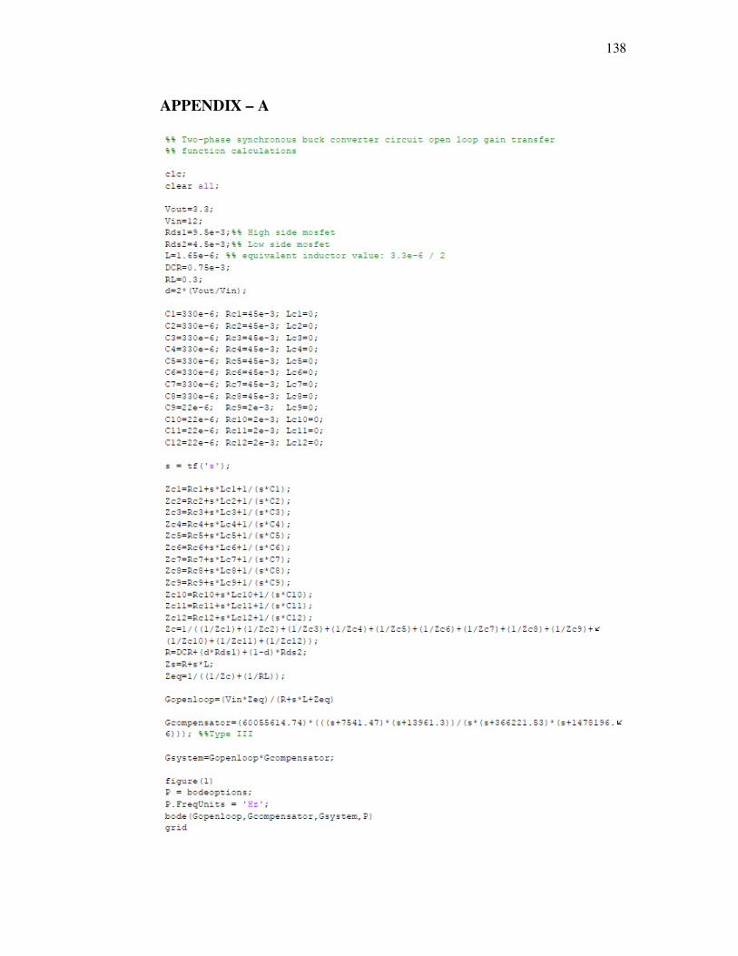
138
APPENDIX – A
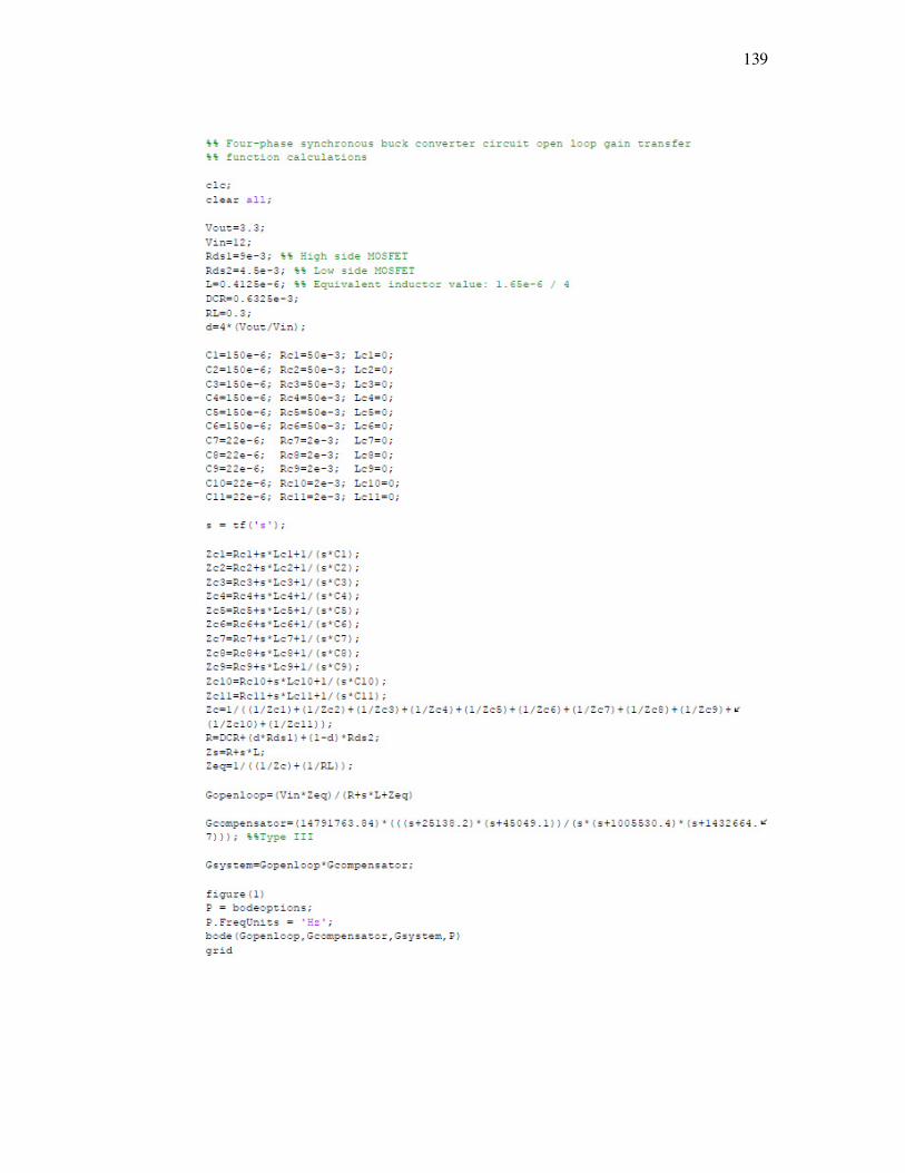
139
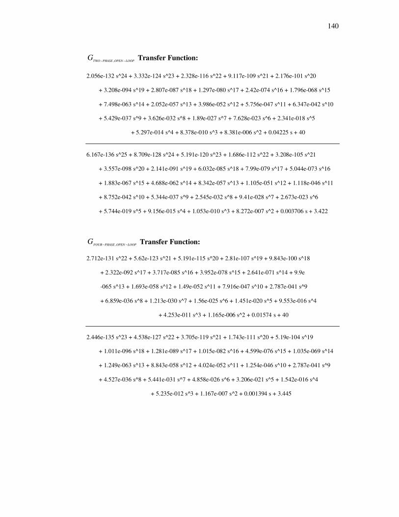
140
LOOPOPENPHASETWOG
−− , Transfer Function:
2.056e-132 s^24 + 3.332e-124 s^23 + 2.328e-116 s^22 + 9.117e-109 s^21 + 2.176e-101 s^20 + 3.208e-094 s^19 + 2.807e-087 s^18 + 1.297e-080 s^17 + 2.42e-074 s^16 + 1.796e-068 s^15 + 7.498e-063 s^14 + 2.052e-057 s^13 + 3.986e-052 s^12 + 5.756e-047 s^11 + 6.347e-042 s^10 + 5.429e-037 s^9 + 3.626e-032 s^8 + 1.89e-027 s^7 + 7.628e-023 s^6 + 2.341e-018 s^5 + 5.297e-014 s^4 + 8.378e-010 s^3 + 8.381e-006 s^2 + 0.04225 s + 40 6.167e-136 s^25 + 8.709e-128 s^24 + 5.191e-120 s^23 + 1.686e-112 s^22 + 3.208e-105 s^21 + 3.557e-098 s^20 + 2.141e-091 s^19 + 6.032e-085 s^18 + 7.99e-079 s^17 + 5.044e-073 s^16 + 1.883e-067 s^15 + 4.688e-062 s^14 + 8.342e-057 s^13 + 1.105e-051 s^12 + 1.118e-046 s^11 + 8.752e-042 s^10 + 5.344e-037 s^9 + 2.545e-032 s^8 + 9.41e-028 s^7 + 2.673e-023 s^6 + 5.744e-019 s^5 + 9.156e-015 s^4 + 1.053e-010 s^3 + 8.272e-007 s^2 + 0.003706 s + 3.422
LOOPOPENPHASEFOURG
−− , Transfer Function: 2.712e-131 s^22 + 5.62e-123 s^21 + 5.191e-115 s^20 + 2.81e-107 s^19 + 9.843e-100 s^18 + 2.322e-092 s^17 + 3.717e-085 s^16 + 3.952e-078 s^15 + 2.641e-071 s^14 + 9.9e -065 s^13 + 1.693e-058 s^12 + 1.49e-052 s^11 + 7.916e-047 s^10 + 2.787e-041 s^9 + 6.859e-036 s^8 + 1.213e-030 s^7 + 1.56e-025 s^6 + 1.451e-020 s^5 + 9.553e-016 s^4 + 4.253e-011 s^3 + 1.165e-006 s^2 + 0.01574 s + 40
2.446e-135 s^23 + 4.538e-127 s^22 + 3.705e-119 s^21 + 1.743e-111 s^20 + 5.19e-104 s^19 + 1.011e-096 s^18 + 1.281e-089 s^17 + 1.015e-082 s^16 + 4.599e-076 s^15 + 1.035e-069 s^14 + 1.249e-063 s^13 + 8.843e-058 s^12 + 4.024e-052 s^11 + 1.254e-046 s^10 + 2.787e-041 s^9 + 4.527e-036 s^8 + 5.441e-031 s^7 + 4.858e-026 s^6 + 3.206e-021 s^5 + 1.542e-016 s^4 + 5.235e-012 s^3 + 1.167e-007 s^2 + 0.001394 s + 3.445
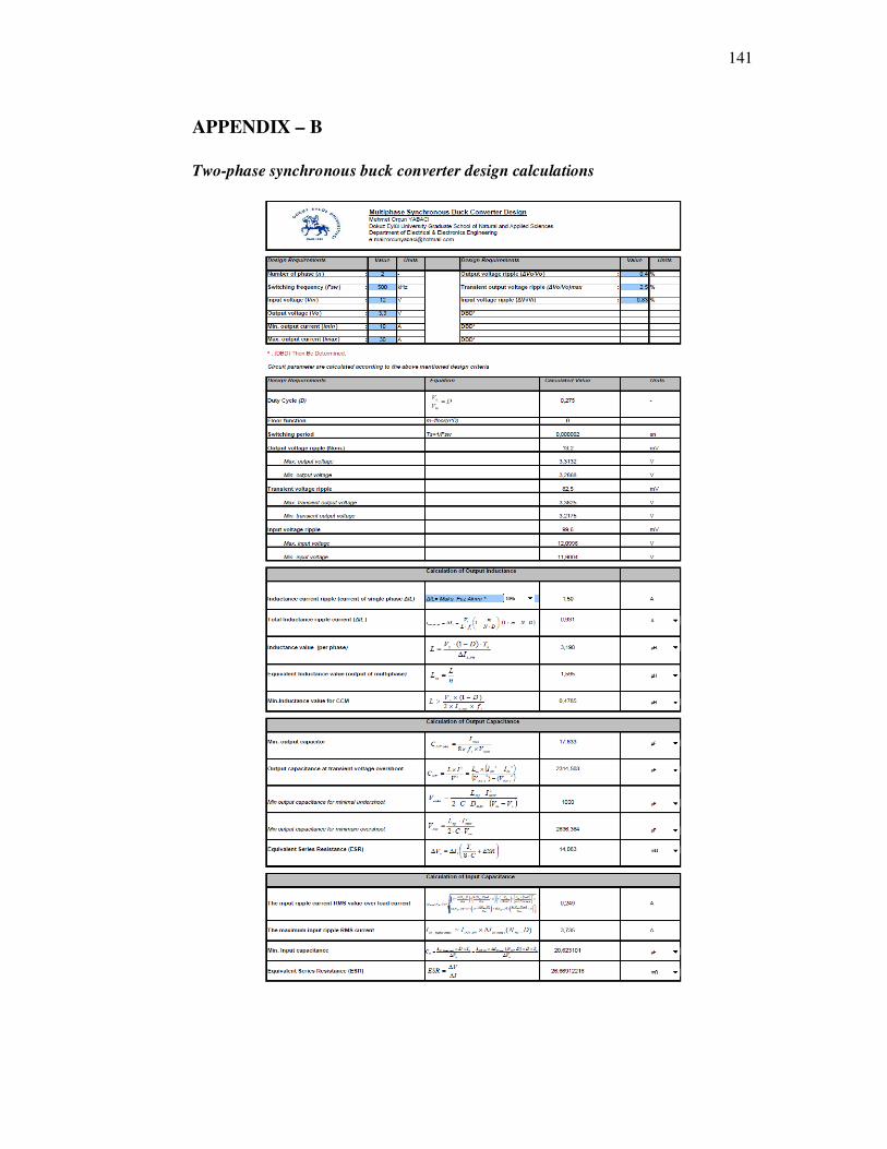
141
APPENDIX – B
Two-phase synchronous buck converter design calculations
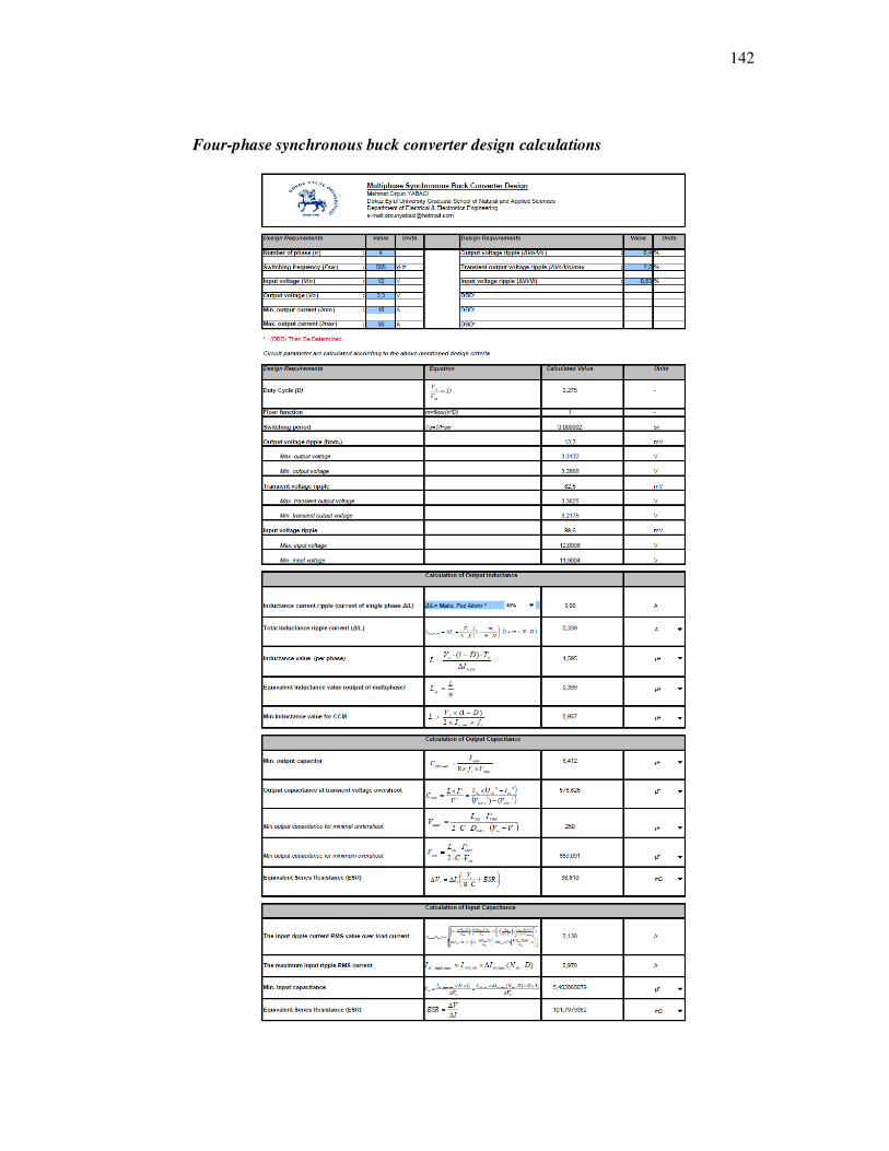
142
Four-phase synchronous buck converter design calculations
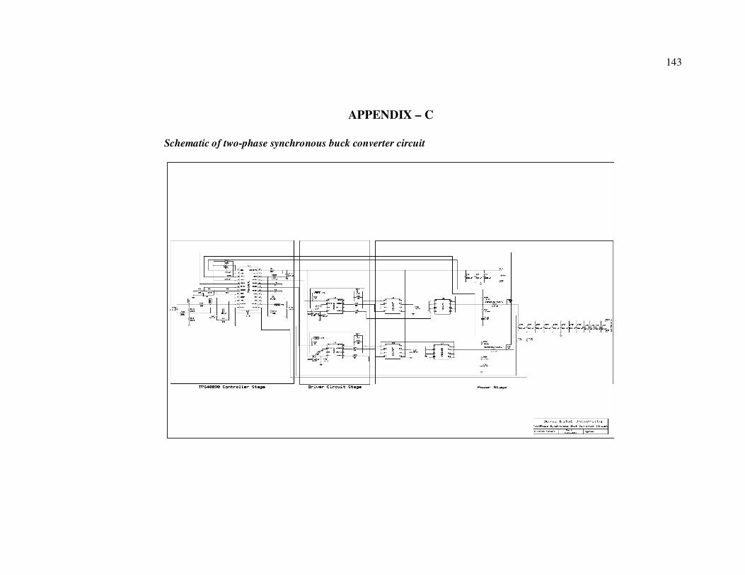
143
APPENDIX – C
Schematic of two-phase synchronous buck converter circuit
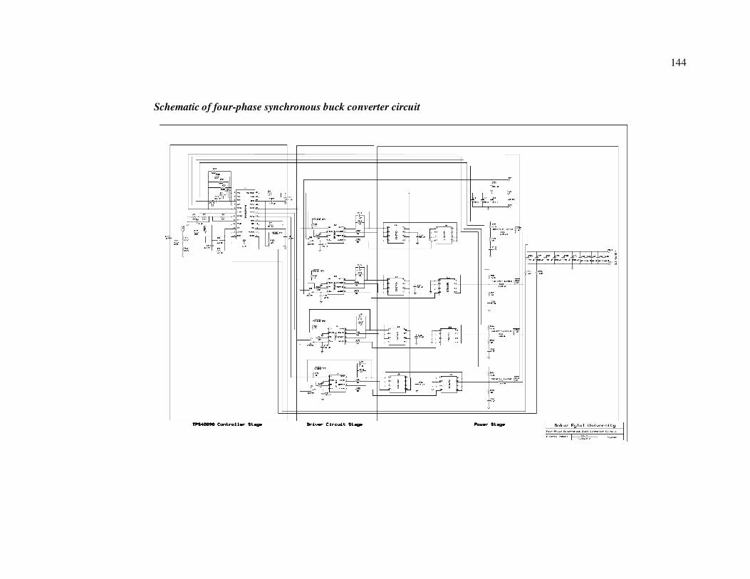
144
Schematic of four-phase synchronous buck converter circuit
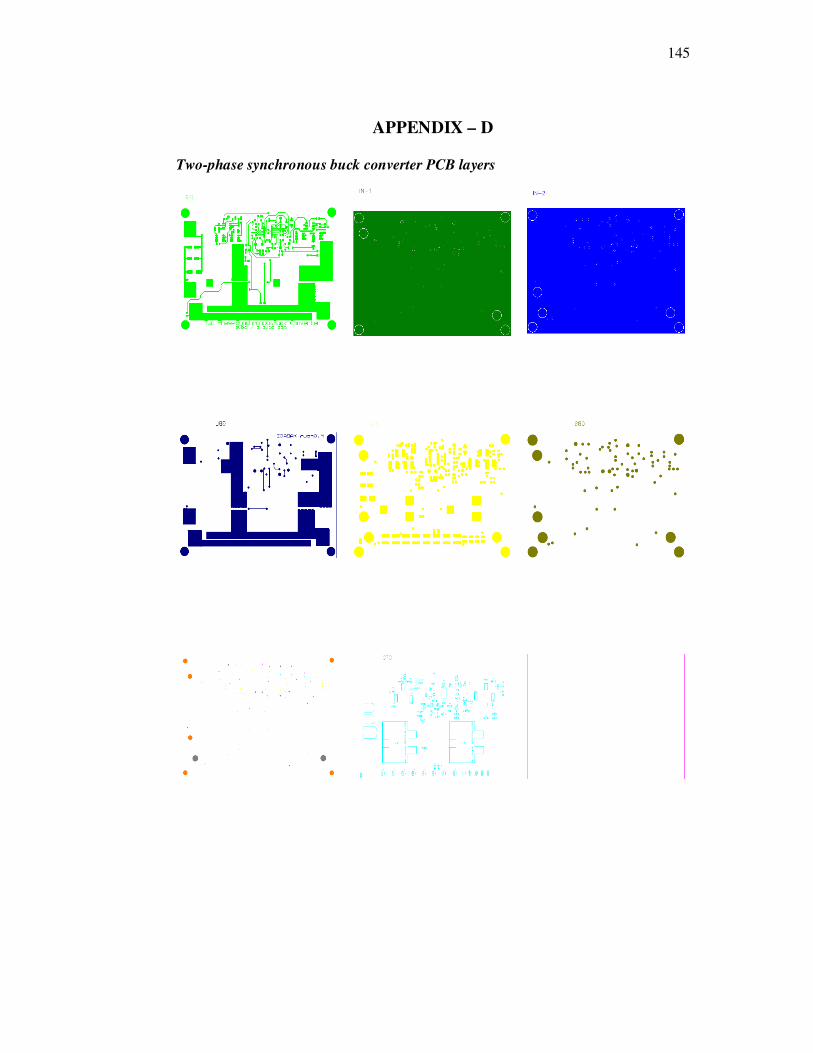
145
APPENDIX – D
Two-phase synchronous buck converter PCB layers
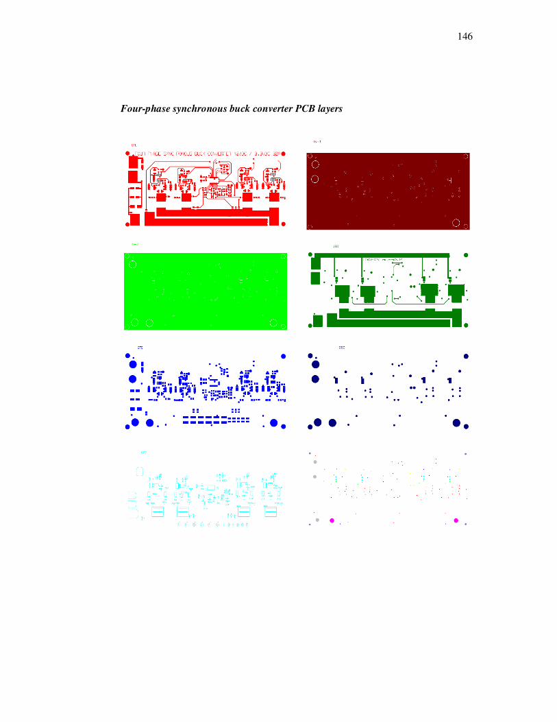
146
Four-phase synchronous buck converter PCB layers