Embed Size (px)
Citation preview

DATA SHEET
Preliminary specificationFile under Integrated Circuits, IC02
1997 Nov 19
INTEGRATED CIRCUITS
TDA9816MMultistandard multimedia IF-PLLand FM radio demodulator

1997 Nov 19 2
Philips Semiconductors Preliminary specification
Multistandard multimedia IF-PLL and FMradio demodulator
TDA9816M
FEATURES
• 5 V supply voltage
• Gain controlled wideband Video IF (VIF) amplifier(AC-coupled)
• True synchronous demodulation with active carrierregeneration (very linear demodulation, goodintermodulation figures, reduced harmonics,excellent pulse response)
• Robustness for over-modulation better than 105% dueto gated phase detector at L/L accent standard and PLLbandwidth control for negative modulation standards
• VCO (Voltage Controlled Oscillator) frequency can beswitched between L and L accent (alignment external)picture carrier frequency
• VIF AGC (Automatic Gain Control) detector for gaincontrol, operating as peak sync detector for B/G andpeak white detector for L; signal controlled reaction timefor L
• Tuner AGC with adjustable TakeOver Point (TOP)
• AFC (Automatic Frequency Control) detector withoutextra reference circuit
• AC-coupled limiting amplifier for sound intercarriersignal
• Alignment-free FM PLL (Phase-Locked Loop)demodulator with high linearity; integrated de-emphasisresistor
• Integrated level detector
• Alignment-free FM radio AFC detector with externalresonator
• RIF (Radio IF) amplifier for 10.7 MHz
• SIF (Sound IF) input for single reference QSS (QuasiSplit Sound) mode (PLL controlled); SIF AGC detectorfor gain controlled SIF amplifier; single reference QSSmixer able to operate in high performance singlereference QSS mode
• AM demodulator without extra reference circuit
• Stabilizer circuit for ripple rejection and to achieveconstant output signals
• ESD (Electrostatic Discharge) protection for all pins.
GENERAL DESCRIPTION
The TDA9816M is an integrated circuit for multistandardvision IF signal processing, sound AM and FMdemodulation and FM radio demodulation in multimediasets.
ORDERING INFORMATION
TYPE NUMBERPACKAGE
NAME DESCRIPTION VERSION
TDA9816M SSOP28 plastic shrink small outline package; 28 leads; body width 5.3 mm SOT341-1

1997 Nov 19 3
Philips Semiconductors Preliminary specification
Multistandard multimedia IF-PLL and FMradio demodulator
TDA9816M
QUICK REFERENCE DATA
Note
1. d3 is the ratio of the intermodulation product at 10.3 MHz to the level of Vi(4)(max)(rms).
SYMBOL PARAMETER CONDITIONS MIN. TYP. MAX. UNIT
Supply (pin 25)
VP supply voltage 4.5 5 5.5 V
IP supply current TV mode (B/G standard) 76 89 102 mA
radio mode 29 35 41 mA
power-down mode 5 8 11 mA
Television mode
Vi(VIF)(rms) minimum vision IF input signalvoltage (RMS value)
−1 dB video at output − 60 100 µV
Vo(video)(p-p) video output signal voltage(peak-to-peak value)
0.97 1.1 1.23 V
B−3dB −3 dB video bandwidth on pin 18 CL < 30 pF; RL > 1.5 kΩ;AC load
7 8 − MHz
S/NW(video) weighted signal-to-noise ratio forvideo
54 58 − dB
αIM(1.1) intermodulation attenuation at ‘blue’ f = 1.1 MHz 52 58 − dB
αIM(3.3) intermodulation attenuation at ‘blue’ f = 3.3 MHz 52 58 − dB
αH(sup) suppression of harmonics in videosignal
35 40 − dB
Vi(SIF)(rms) minimum sound IF input signalvoltage (RMS value)
−3 dB at intercarrier output − 30 70 µV
Vo(audio)(rms) audio output signal voltage for FM(RMS value)
B/G standard;27 kHz modulation
0.4 0.5 0.6 V
THDvideo total harmonic distortion for video 27 kHz modulation − 0.5 1.0 %
S/NW(audio) weighted signal-to-noise ratio foraudio
27 kHz modulation; t = 50 µs 50 55 − dB
Radio mode
Vi(RIF)(rms) minimum radio IF input signalvoltage (RMS value)
d3 < 60 dB intermodulation;note 1
− − 20 mV
Vi(FM)(rms) minimum FM limiter input signalvoltage (RMS value)
− 100 − µV
∆VLD/log∆Vi output voltage slope according toFM limiter input voltage
− 50 − mV/dBµV
Vo(audio)(rms) audio output signal voltage for radio(peak-to-peak value)
22.5 kHz modulation 200 250 300 mV
THDaudio total harmonic distortion for audio 22.5 kHz modulation − 0.5 1.0 %
S/NW(audio) weighted signal-to-noise ratio foraudio
22.5 kHz modulation;15 kHz bandwidth
59 64 − dB
S N+N
-------------- unweighted 26 dB=
1997 Nov 19 4
Philips Semiconductors Preliminary specification
Multistandard multimedia IF-PLL and FMradio demodulator
TDA9816M
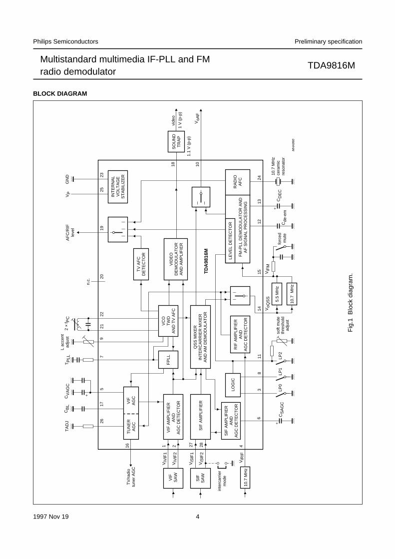
BLOCK DIAGRAM
ok, full pagewidth
1 V
(p-
p)
MH
A99
0
VC
OT
WD
AN
D T
V A
FC
QS
S M
IXE
RIN
TE
RC
AR
RIE
R M
IXE
RA
ND
AM
DE
MO
DU
LAT
OR
FP
LL
SIF
AM
PLI
FIE
R
RIF
AM
PLI
FIE
RA
ND
AG
C D
ET
EC
TO
R
VIF
AM
PLI
FIE
RA
ND
AG
C D
ET
EC
TO
R
SIF
AM
PLI
FIE
RA
ND
AG
C D
ET
EC
TO
R
TU
NE
RA
GC
VIF
AG
C
VIF
SA
WS
OU
ND
TR
AP
VID
EO
DE
MO
DU
LAT
OR
AN
D A
MP
LIF
IER
TV
AF
CD
ET
EC
TO
R
INT
ER
NA
LV
OLT
AG
ES
TA
BIL
IZE
R
GN
D
n.c.
VP
AF
C/R
IFle
vel
2 ×
f PC
TP
LLC
VA
GC
TA
DJ
TV
/rad
iotu
ner
AG
C
116 2
LOG
IC
4
38
CD
EC
forc
ed m
ute
soft
mut
eth
resh
old
adju
st
LP1
LP0
11 LP2
5.5
MH
z
13
Cde
-em
1224
1514
18 10
1925
2221
75
2623
VoA
F
1.1
V (
p-p)
vide
o
20
TD
A98
16M
10.7
MH
z
10.7
MH
z
10.7
MH
zce
ram
icre
sona
tor
FM
-PLL
DE
MO
DU
LAT
OR
AN
DA
F S
IGN
AL
PR
OC
ES
SIN
G
LEV
EL
DE
TE
CT
OR
RA
DIO
AF
C
inte
rcar
rier
mod
e
CS
AG
C
6
SIF
SA
W
ViV
IF1
ViV
IF2
ViS
IF1
ViS
IF2
ViR
IF
VoQ
SS
ViF
M
2827
179
CB
LL
acce
ntad
just
Fig
.1 B
lock
dia
gram
.

1997 Nov 19 5
Philips Semiconductors Preliminary specification
Multistandard multimedia IF-PLL and FMradio demodulator
TDA9816M
PINNING
SYMBOL PIN DESCRIPTION
ViVIF1 1 VIF differential input signal voltage 1
ViVIF2 2 VIF differential input signal voltage 2
LP0 3 logic port 0
ViRIF 4 RIF input
CVAGC 5 VIF AGC capacitor
CSAGC 6 SIF AGC capacitor
TPLL 7 PLL loop filter
LP1 8 logic port 1
LADJ 9 L/L accent switch and adjustment
VoAF 10 audio output
LP211
logic port 2 and soft mute thresholdadjustment
Cde-em 12 de-emphasis capacitor
CDEC 13 decoupling capacitor
VoQSS 14single reference QSS/intercarrieroutput voltage
ViFM 15 sound intercarrier input voltage
TAGC 16 TV/radio tuner AGC output
CBL 17 black level detector
Vo(vid) 18 composite video output voltage
AFC 19 AFC/RIF level output
n.c. 20 not connected
VCO1 21 VCO1 resonance circuit
VCO2 22 VCO2 resonance circuit
GND 23 ground
CERRES 24 ceramic resonator 10.7 MHz
VP 25 supply voltage
TADJ 26 tuner AGC takeover point adjustment
ViSIF1 27 SIF differential input signal voltage 1
ViSIF2 28 SIF differential input signal voltage 2Fig.2 Pin configuration.
handbook, halfpageViVIF1
ViVIF2
LP0
ViRIF
CVAGC
CSAGC
TPLL
LP1
LADJ
VoAF
LP2
Cde-em
CDEC
VoQSS
ViSIF2
ViSIF1
TADJ
VP
GND
VCO2
CERRES
VCO1
n.c.
AFC
Vo(vid)
CBL
TAGC
ViFM
1
2
3
4
5
6
7
8
9
10
11
12
13
28
27
26
25
24
23
22
21
20
19
18
17
16
1514
TDA9816M
MHA989
1997 Nov 19 6
Philips Semiconductors Preliminary specification
Multistandard multimedia IF-PLL and FMradio demodulator
TDA9816M
FUNCTIONAL DESCRIPTION
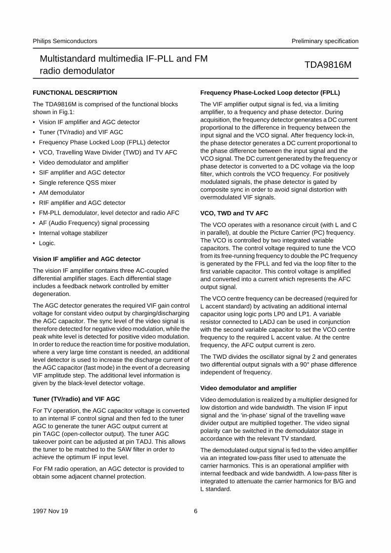
The TDA9816M is comprised of the functional blocksshown in Fig.1:
• Vision IF amplifier and AGC detector
• Tuner (TV/radio) and VIF AGC
• Frequency Phase Locked Loop (FPLL) detector
• VCO, Travelling Wave Divider (TWD) and TV AFC
• Video demodulator and amplifier
• SIF amplifier and AGC detector
• Single reference QSS mixer
• AM demodulator
• RIF amplifier and AGC detector
• FM-PLL demodulator, level detector and radio AFC
• AF (Audio Frequency) signal processing
• Internal voltage stabilizer
• Logic.
Vision IF amplifier and AGC detector
The vision IF amplifier contains three AC-coupleddifferential amplifier stages. Each differential stageincludes a feedback network controlled by emitterdegeneration.
The AGC detector generates the required VIF gain controlvoltage for constant video output by charging/dischargingthe AGC capacitor. The sync level of the video signal istherefore detected for negative video modulation, while thepeak white level is detected for positive video modulation.In order to reduce the reaction time for positive modulation,where a very large time constant is needed, an additionallevel detector is used to increase the discharge current ofthe AGC capacitor (fast mode) in the event of a decreasingVIF amplitude step. The additional level information isgiven by the black-level detector voltage.
Tuner (TV/radio) and VIF AGC
For TV operation, the AGC capacitor voltage is convertedto an internal IF control signal and then fed to the tunerAGC to generate the tuner AGC output current atpin TAGC (open-collector output). The tuner AGCtakeover point can be adjusted at pin TADJ. This allowsthe tuner to be matched to the SAW filter in order toachieve the optimum IF input level.
For FM radio operation, an AGC detector is provided toobtain some adjacent channel protection.
Frequency Phase-Locked Loop detector (FPLL)
The VIF amplifier output signal is fed, via a limitingamplifier, to a frequency and phase detector. Duringacquisition, the frequency detector generates a DC currentproportional to the difference in frequency between theinput signal and the VCO signal. After frequency lock-in,the phase detector generates a DC current proportional tothe phase difference between the input signal and theVCO signal. The DC current generated by the frequency orphase detector is converted to a DC voltage via the loopfilter, which controls the VCO frequency. For positivelymodulated signals, the phase detector is gated bycomposite sync in order to avoid signal distortion withovermodulated VIF signals.
VCO, TWD and TV AFC
The VCO operates with a resonance circuit (with L and Cin parallel), at double the Picture Carrier (PC) frequency.The VCO is controlled by two integrated variablecapacitors. The control voltage required to tune the VCOfrom its free-running frequency to double the PC frequencyis generated by the FPLL and fed via the loop filter to thefirst variable capacitor. This control voltage is amplifiedand converted into a current which represents the AFCoutput signal.
The VCO centre frequency can be decreased (required forL accent standard) by activating an additional internalcapacitor using logic ports LP0 and LP1. A variableresistor connected to LADJ can be used in conjunctionwith the second variable capacitor to set the VCO centrefrequency to the required L accent value. At the centrefrequency, the AFC output current is zero.
The TWD divides the oscillator signal by 2 and generatestwo differential output signals with a 90° phase differenceindependent of frequency.
Video demodulator and amplifier
Video demodulation is realized by a multiplier designed forlow distortion and wide bandwidth. The vision IF inputsignal and the ‘in-phase’ signal of the travelling wavedivider output are multiplied together. The video signalpolarity can be switched in the demodulator stage inaccordance with the relevant TV standard.
The demodulated output signal is fed to the video amplifiervia an integrated low-pass filter used to attenuate thecarrier harmonics. This is an operational amplifier withinternal feedback and wide bandwidth. A low-pass filter isintegrated to attenuate the carrier harmonics for B/G andL standard.
1997 Nov 19 7
Philips Semiconductors Preliminary specification
Multistandard multimedia IF-PLL and FMradio demodulator
TDA9816M
The standard-dependent level shift in this stage deliversthe same sync level for positive and negative modulation.The video output signal at Vo(vid) is 1.1 V (p-p) for nominalvision IF modulation, in order to achieve 1 V (p-p) at thesound trap output.
SIF amplifier and AGC
The sound IF amplifier consists of two AC-coupleddifferential amplifier stages. Each differential stage iscomprised of a controlled feedback network provided byemitter degeneration.
The SIF AGC detector is related to the SIF input signal(average level of AM or FM carrier). It controls the SIFamplifier to provide a constant SIF signal to theAM demodulator and single reference QSS mixer.The AGC reaction time is set to ‘slow’ for nominal videoconditions. But with a decreasing VIF amplitude step theSIF AGC is set to ‘fast’ mode, controlled by the VIF AGCdetector. In FM mode this reaction time is also set to ‘fast’mode according to the TV standard.
Single reference QSS mixer
The single reference QSS mixer is realized by a multiplier.The SIF amplifier output signal is fed to the singlereference QSS mixer and converted to the intercarrierfrequency by the regenerated picture carrier (VCO).The mixer output signal is fed, via a high-pass filter usedto attenuate the video signal components, to output pin 14.High performance hi-fi stereo sound processing can beachieved with this system.
For a simplified application without a sound IF SAW filter,the single reference QSS mixer can be switched to theintercarrier mode by connecting pin 27 and/or pin 28 toground. In this mode, the sound IF signal passes throughthe vision IF SAW filter and the composite IF signal is thenfed to the single reference QSS mixer. Here, the IF signalis multiplied by the 90° TWD output signal to convert thesound IF to the intercarrier frequency. By using thisquadrature detection, the low frequency video signals areremoved.
AM demodulator
A multiplier is used for AM demodulation. The modulatedSIF amplifier output signal and the ‘in-phase’ limited(AM is removed) SIF amplifier output signal are multipliedtogether. The demodulated output signal is fed, via anintegrated low-pass filter used to attenuate the carrierharmonics, to the AF amplifier.
RIF amplifier and AGC
The radio IF amplifier amplifies the 10.7 MHz radio IFsignal. This signal is supplied by the tuner and is fed to theRIF input (pin 4) via a matching circuit and a ceramicband-pass filter. This amplifier contains two stages.The first stage, a conventional 0 dB differential amplifierdesigned for optimal dynamic range, is followed by aswitchable differential amplifier stage with a gain of 10 dB.Either the radio IF or to the TV IF signal can be selected atthe output (pin 14).
The RIF output signal is fed via ceramic band-pass filtersto the FM-PLL demodulator and the radio IF AGC detector.The AGC threshold is very high and is designed to obtainsome adjacent channel protection. The AGC detectoroutput is fed to the tuner AGC output stage (pin 16) tocontrol the tuner.
FM-PLL demodulator level detector and radio AFC
The FM-PLL demodulator consists of a limiter and an FMphase-locked loop. The 8-stage internally AC-coupledlimiter amplifies and limits the TV FM sound intercarrier orthe radio FM intermediate frequency signal prior todemodulation. The limiter is designed for high sensitivityand AM suppression with low DC offset and needs noexternal pins for DC coupling.
Furthermore, the AF output signal can be force muted byconnecting a resistor between pin 15 and ground. The softmute function can be disabled by connecting a resistorbetween pin 15 and the power supply. See the applicationcircuit in Fig.18.
The FM-PLL consists of an integrated relaxation oscillator,an integrated loop filter and a phase detector.The oscillator is locked to the FM intercarrier signal outputfrom the limiter. As a result of locking, the oscillatorfrequency tracks with the modulation of the input signaland the oscillator control voltage is superimposed on theAF voltage. The FM-PLL operates as an FM demodulator.
The level detector detects, rectifies and amplifies theoutput signals from the first 5 limiter stages. These signalsare then summed and the composite signal passedthrough a low-pass filter, followed by a 6 dB outputamplifier. A DC voltage dependent on the limiter input levelis generated for controlling the behaviour of the AF softmute. The 6 dB output amplifier can be switched off via thecontrol logic and the level detector output signal fed topin 19. Furthermore, the steepness of the level detectoroutput signal tracks that of the power supply voltage.

1997 Nov 19 8
Philips Semiconductors Preliminary specification
Multistandard multimedia IF-PLL and FMradio demodulator
TDA9816M
The radio Automatic Frequency Control (AFC) stage iscomprised of a 10.7 MHz phase shifting network, a phasedetector (quadrature demodulator), a differential amplifierinput stage (which receives the limiting amplifier outputsignal), and a current mode output stage.
A ceramic resonator is used for phase shifting. Thispermits alignment-free operation.
AF signal processing
The AF signal processing stage consists of a pre-amplifierfor the FM-PLL demodulator output signal, an AF sourceselector, a soft and forced mute stage with an integratedtime constant, and an AF post-amplifier.
The FM demodulator output signal is pre-amplified by anoperational amplifier (30 dB gain) with internal feedback,high gain and high common mode rejection. The feedbackcircuit, together with external capacitor CDEC connected topin 13, keeps the DC level at the pre-amplifier outputconstant (2.3 V). An external resistor connected in serieswith CDEC provides a gain-reduction capability.The low-pass filter characteristic (130 kHz bandwidth) ofthe amplifier reduces the harmonics of the IF signal at thesound signal output.
The source selector operational amplifier selects andamplifies the appropriate AF source signal by means of thecontrol logic: AM from the AM demodulator in TV L/Laccent mode, FM from the FM demodulator viade-emphasis (internal resistor, external capacitor Cde-em atpin 12) in TV B/G mode or FM direct from the FMdemodulator in radio mode.
Soft mute occurs when the internal level detector outputvoltage is lower than the mute threshold voltage at pin 11(provided an external resistor is not connected betweenthe limiter input, pin 15, and the supply voltage). The mutestage reduces the AF signal by 25 dB, with an internal timeconstant of approximately 7 ms.
If forced mute is active (see Table 2), or a resistor isconnected between pin 15 and ground, the mute stage willreduce the AF signal level by more than 70 dB, with thesame time constant.
Otherwise, the AF signal level will not be reduced.
The AF post-amplifier, which was designed to include arail-to-rail output stage, provides the required AF outputlevel at pin 10.
Internal voltage stabilizer
The band gap circuit generates a voltage of approximately1.25 V internally, independent of supply voltage andtemperature. A voltage regulator circuit connected to thisvoltage generates a constant 3.6 V which is used as aninternal reference voltage.
Logic
The logic circuit detects the logic levels and thresholdvoltages at ports LP0, LP1 and LP2 and controls theinternal functions as described in Table 2.

1997 Nov 19 9
Philips Semiconductors Preliminary specification
Multistandard multimedia IF-PLL and FMradio demodulator
TDA9816M
LIMITING VALUESIn accordance with the Absolute Maximum Rating System (IEC 134).
Notes
1. IP = 102 mA; Tamb = 70 °C; Rth(j-a) = 110 K/W.
2. Machine model class B (L = 2.5 µH).
THERMAL CHARACTERISTICS
SYMBOL PARAMETER CONDITIONS MIN. MAX. UNIT
VP supply voltage (pin 25) maximum chip temperatureof 125 °C; note 1
− 5.5 V
Vn input voltage at pins 1 to 13, 15 to 17,19 and 23 to 28
0 VP V
tsc short-circuit time − 10 s
VTAGC tuner AGC output voltage 0 13.2 V
Tstg storage temperature −25 +150 °CTamb operating ambient temperature −20 +70 °CVes electrostatic handling voltage note 2 −300 +300 V
SYMBOL PARAMETER CONDITIONS VALUE UNIT
Rth(j-a) thermal resistance from junction to ambient in free air 110 K/W

1997 Nov 19 10
Philips Semiconductors Preliminary specification
Multistandard multimedia IF-PLL and FMradio demodulator
TDA9816M
CHARACTERISTICSVP = 5 V; Tamb = 25 °C; see Table 1 for input frequencies; input level Vi(VIF)(rms) = 10 mV (sync-level for B/G,peak white level for L); Vi(FM)(rms) = 10 mV; IF input from 50 Ω via broadband transformer 1 : 1; video modulation DSB;residual carrier B/G: 10%; L = 3%; video signal in accordance with “CCIR, line 17”; measured in test circuit of Fig.17;unless otherwise specified.
SYMBOL PARAMETER CONDITIONS MIN. TYP. MAX. UNIT
Supply (pin 25)
VP supply voltage note 1 4.5 5 5.5 V
IP supply current TV mode (B/G standard) 76 89 102 mA
radio mode 29 35 41 mA
power-down mode 5 8 11 mA
Television mode
VISION IF AMPLIFIER (PINS 1 AND 2)
Vi(VIF)(rms) minimum vision IF inputsignal voltage(RMS value)
B/G standard; −1 dB videoat output
− 60 100 µV
maximum vision IF inputsignal voltage(RMS value)
B/G standard; +1 dB videoat output
120 200 − mV
∆Vo(int) internal IF amplitudedifference betweenpicture and sound carrier
within AGC range;B/G standard;∆f = 5.5 MHz
− 0.7 1 dB
GVIF(CR) VIF gain control range see Fig.3 65 70 − dB
BVIF(−3dB) −3 dB VIF bandwidth lower limit − 15 25 MHz
upper limit 70 100 − MHz
Ri(dif) differential inputresistance
note 2 1.7 2.2 2.7 kΩ
Ci(dif) differential inputcapacitance
note 2 1.2 1.7 2.5 pF
VI DC input voltage note 2 − 3.4 − V
TRUE SYNCHRONOUS VIDEO DEMODULATOR; note 3
fVCO(max) maximum oscillatorfrequency for carrierregeneration
f = 2fPC 125 130 − MHz
∆fosc/∆T oscillator drift as afunction of temperature
oscillator is free-running;IAFC = 0; note 4
− − ±20 × 10−6 K−1
VVCO(rms) oscillator voltage swing atpins 21 and 22(RMS value)
50 80 110 mV
fcr(PC ) picture carrier capturerange
B/G and L standard ±1.4 ±1.8 − MHz
L accent standard;fPC = 33.9 MHz;R9 = 5.6 kΩ
±0.9 ±1.2 − MHz

1997 Nov 19 11
Philips Semiconductors Preliminary specification
Multistandard multimedia IF-PLL and FMradio demodulator
TDA9816M
∆ffr(PC ) picture carrierfree-running frequencyaccuracy
L accent standard;fPC = 33.9 MHz;R9 = 5.6 kΩ
− ±200 ±400 kHz
falg(L accent) L accent alignmentfrequency range
L accent standard; IAFC = 0 ±400 ±600 − kHz
tacq acquisition time Black Level (BL) = 70 kHznote 5
− − 30 ms
Vi(VIF)(rms) minimum vision IF inputsignal voltage for PLL tobe locked (RMS value;pins 1 and 2)
maximum IF gain; note 6 − 30 70 µV
COMPOSITE VIDEO AMPLIFIER (PIN 18; SOUND CARRIER OFF)
Vo(video)(p-p) output signal voltage(peak-to-peak value)
see Fig.8 0.97 1.1 1.23 V
V/S ratio between video(black-to-white) andsync level
1.9 2.33 3.0 −
∆Vo(video) output signal voltagedifference
difference betweenB/G and L standard
− − ±12 %
Vsync sync voltage level B/G and L standard 1.4 1.5 1.6 V
Vclu upper video clippingvoltage level
VP − 1.1 VP − 1 − V
Vcll lower video clippingvoltage level
− 0.7 0.9 V
Ro output resistance note 2 − − 10 ΩIbias(int) internal DC bias current
for emitter-follower2.2 3.0 − mA
Io(sink)(max) maximum AC and DCoutput sink current
1.6 − − mA
Io(source)(max) maximum AC and DCoutput source current
2.9 − − mA
∆Vo(CVBS) deviation of CVBS outputsignal voltage at B/G
50 dB gain control − − 0.5 dB
30 dB gain control − − 0.1 dB
∆Vo(bl)(BG) black level tilt inB/G standard
gain variation; note 7 − − 1 %
∆Vo(bl)(L) vertical black level tilt forworst case in L standard
vision carrier modulatedby test line (VITS) only;gain variation; note 7
− − 1.9 %
Gdif differential gain “CCIR, line 330” − 2 5 %
ϕdif differential phase “CCIR, line 330” − 1 2 deg
Bv(−1dB) −1 dB video bandwidth B/G and L standard;CL < 50 pF; RL > 1 kΩ;AC load
5 6 − MHz
SYMBOL PARAMETER CONDITIONS MIN. TYP. MAX. UNIT

1997 Nov 19 12
Philips Semiconductors Preliminary specification
Multistandard multimedia IF-PLL and FMradio demodulator
TDA9816M
Bv(−3dB) −3 dB video bandwidth B/G and L standard;CL < 50 pF; RL > 1 kΩ;AC load
7 8 − MHz
S/NW weighted signal-to-noiseratio
see Fig.5 and note 8 54 58 − dB
S/N unweightedsignal-to-noise ratio
see Fig.5 and note 8 47 51 − dB
αIM(1.1) intermodulationattenuation at ‘blue’
fIM = 1.1 MHz; see Fig.6and note 9
52 58 − dB
intermodulationattenuation at ‘yellow’
fIM = 1.1 MHz; see Fig.6and note 9
54 60 − dB
αIM(3.3) intermodulationattenuation at ‘blue’
fIM = 3.3 MHz; see Fig.6and note 9
52 58 − dB
intermodulationattenuation at ‘yellow’
fIM = 3.3 MHz; see Fig.6and note 9
54 60 − dB
αr(vc)(rms) residual vision carrier(RMS value)
fundamental wave andharmonics;B/G and L standard
− 2 5 mV
∆funwanted(p-p) robustness for unwantedfrequency deviation ofpicture carrier(peak-to-peak value)
L standard;residual carrier: 3%;serration pulses: 50%;note 2
− − 12 kHz
∆ϕ robustness for modulatorimbalance
L standard;residual carrier: 0%;serration pulses: 50%;note 2
− − 3 %
αH(sup) suppression of videosignal harmonics
note 10a 35 40 − dB
αH(spur) spurious elements note 10b 40 − − dB
PSRR power supply ripplerejection at pin 18
video signal; grey level;see Fig.11
B/G standard 30 35 − dB
L standard 25 30 − dB
VIF AGC DETECTOR (PIN 5)
Ich charge current B/G and L standard; note 7 0.75 1 1.25 mA
additional charge current L standard in event ofmissing VITS pulses andno white video content
1.9 2.5 3.1 µA
Idch discharge current B/G standard 15 20 25 µA
normal mode L standard 225 300 375 nA
fast mode L standard 30 40 50 µA
tres(AGC)(r) AGC response to a risingVIF step
B/G and L standard;note 11
− 0.05 0.1 ms/dB
SYMBOL PARAMETER CONDITIONS MIN. TYP. MAX. UNIT

1997 Nov 19 13
Philips Semiconductors Preliminary specification
Multistandard multimedia IF-PLL and FMradio demodulator
TDA9816M
tres(AGC)(f) AGC response to a fallingVIF step
B/G standard − 2.2 3.5 ms/dB
fast mode L standard − 1.1 1.8 ms/dB
normal mode L standard;note 11
− 150 240 ms/dB
∆IF VIF amplitude step foractivating fast AGC mode
L standard −2 −6 −10 dB
Vth(17) threshold voltage leveladditional charging/discharging current
see Fig.8
L standard 1.95 2.0 2.05 V
L standard; fast mode L 1.6 1.66 1.72 V
TV TUNER AGC (PIN 16)
Vi(rms) IF input signal voltage forminimum starting point oftuner takeover(RMS value)
input at pins 1 and 2;RTOP = 22 kΩ; I16 = 0.4 mA
− 2 5 mV
IF input signal voltage formaximum starting point oftuner takeover(RMS value)
input at pins 1 and 2;RTOP = 0 Ω; I16 = 0.4 mA
50 100 − mV
tuner takeover pointaccuracy (RMS value)
RTOP = 13 kΩ; I16 = 0.4 mA 5 − 20 mV
Vo(max) maximum output voltage from external source;note 2
− − 13.2 V
Vsat saturation voltage I16 = 1.5 mA − − 0.2 V
∆VTOP(T) variation of takeover pointwith temperature
I16 = 0.4 mA − 0.03 0.07 dB/K
Isink sink current see Fig.3
no tuner gain reduction;V16 = 13.2 V
− − 1 µA
maximum tuner gainreduction
1.5 2 2.6 mA
∆GIF IF slip by automatic gaincontrol
tuner gain current from20 to 80%
− 6 8 dB
TV AFC DETECTOR (PIN 19); see Fig.7 and note 12
CRstps control steepness ∆I19/∆f note 13 0.5 0.75 1.0 µA/kHz
∆fIF(T) frequency variation withtemperature
IAFC = 0; note 4
B/G and L standard − − ±20 × 10−6 K−1
L accent standard − − ±60 × 10−6 K−1
Vo(max) output voltage upper limit see Fig.7 without externalcomponents
VP − 0.6 VP − 0.3 − V
Vo(min) output voltage lower limit − 0.3 0.6 V
Io(source) output source current 150 200 250 µA
Io(sink) output sink current 150 200 250 µA
SYMBOL PARAMETER CONDITIONS MIN. TYP. MAX. UNIT

1997 Nov 19 14
Philips Semiconductors Preliminary specification
Multistandard multimedia IF-PLL and FMradio demodulator
TDA9816M
∆Ir(mod)(p-p) residual video modulationcurrent(peak-to-peak value)
B/G and L standard − 20 30 µA
SOUND IF AMPLIFIER (PINS 27 AND 28)
Vi(SIF)(rms) minimum sound IF inputsignal voltage(RMS value)
FM mode; −3 dB atintercarrier output pin 14
− 30 70 µV
AM mode; −3 dB atAF output pin 10
− 70 100 µV
Vi(max)(rms) maximum sound IF inputsignal voltage(RMS value)
FM mode; +1 dB atintercarrier output pin 14
50 70 − mV
AM mode; +1 dB atAF output pin 10
80 140 − mV
Gcr(SIF) SIF gain control range FM and AM mode;see Fig.4
60 67 − dB
BSIF(−3dB) −3 dB SIF bandwidth lower limit − − 25 MHz
upper limit 60 − − MHz
Ri(dif) differential inputresistance
note 2 1.7 2.2 2.7 kΩ
Ci(dif) differential inputcapacitance
note 2 1.2 1.7 2.5 pF
VI(27,28) DC input voltage − 3.4 − V
αct(SIF-VIF) crosstalk attenuationbetween SIF and VIFinput
between pins 1 and 2 andpins 27 and 28; note 14
50 − − dB
SIF-AGC DETECTOR (PIN 6)
Ich charge current FM mode 8 12 16 µA
AM mode 0.8 1.2 1.6 µA
Idch discharge current FM mode 8 12 16 µA
normal mode AM 1 1.4 1.8 µA
fast mode AM 60 85 110 µA
SINGLE REFERENCE QSS INTERCARRIER MIXER (PIN 14)
Vo(intercarrier)(rms) IF intercarrier level(RMS value)
QSS mode; SC1;sound carrier 2 off
100 140 180 mV
L standard;without modulation
100 140 180 mV
intercarrier mode; SC1;sound carrier 2 off; note 15
− 32 − mV
Bic(−3dB) −3 dB intercarrierbandwidth
upper limit 7.5 9 − MHz
SYMBOL PARAMETER CONDITIONS MIN. TYP. MAX. UNIT

1997 Nov 19 15
Philips Semiconductors Preliminary specification
Multistandard multimedia IF-PLL and FMradio demodulator
TDA9816M
αr(SC)(rms) residual sound carrier(RMS value)
QSS mode; fundamentalwave and harmonics
− 2 5 mV
intercarrier mode;fundamental wave andharmonics
− 2 5 mV
αr(VC)(rms) residual vision carrier(RMS value)
QSS mode; fundamentalwave and harmonics
− 2 5 mV
intercarrier mode;fundamental wave andharmonics
− 2 5 mV
αH(sup) suppression of videosignal harmonics
intercarrier mode;fvideo ≤ 5 MHz
39 − − dB
Ro output resistance note 2 − 25 − ΩVO DC output voltage − 2.0 − V
Ibias(int) DC internal bias currentfor emitter-follower
2.7 3.4 − mA
I(sink)(max) maximum AC and DCoutput sink current
1.5 2.0 − mA
I(source)(max) maximum AC and DCoutput source current
2.5 − − mA
LIMITER AMPLIFIER (PIN 15); note 16
Vi(FM)(rms) input signal voltage forlock-in (RMS value)
− − 100 µV
input signal voltage(RMS value)
− 250 500 µV
allowed input signalvoltage (RMS value)
200 − − mV
αAM AM suppression 50 µs de-emphasis;AM: fmod = 1 kHz; m = 0.3referenced to 27 kHz(54% FM deviation)
46 50 − dB
Ri input resistance note 2 480 600 720 ΩVI DC input voltage − 2.65 − V
FM-PLL DEMODULATOR
fcr(PLL) catching range of PLL upper limit 7.0 − − MHz
lower limit − − 4.0 MHz
fhr(PLL) holding range of PLL upper limit 9.0 − − MHz
lower limit − − 3.5 MHz
tacq acquisition time − − 4 µs
SYMBOL PARAMETER CONDITIONS MIN. TYP. MAX. UNIT
S N+N
-------------- weighted 40 dB=

1997 Nov 19 16
Philips Semiconductors Preliminary specification
Multistandard multimedia IF-PLL and FMradio demodulator
TDA9816M
FM OPERATION (B/G STANDARD; PIN 10); notes 16 and 16a
Vo(AF)(rms) AF output signal voltage(RMS value)
27 kHz(54% FM deviation);see Fig.17 and note 17
Rx = 470 Ω 200 250 300 mV
Rx = 0 Ω 400 500 600 mV
Vo(AF)(cl)(rms) AF output clipping signalvoltage level (RMS value)
THD < 1.5% 1.0 − 1.2 V
∆fAF frequency deviation THD < 1.5%; note 17 − − ±53 kHz
∆Vo/∆T temperature drift of AFoutput signal voltage
− 3 × 10⁻³ 7 × 10⁻³ dB/K
V13 DC voltage at decouplingcapacitor
voltage dependent on VCOfrequency; note 18
1.2 − 3.0 V
Ro output resistance note 2 − − 150 ΩVO DC output voltage − 2.3 − V
Io(sink)(max) maximum AC and DCoutput sink current
− − 0.5 mA
Io(source)(max) maximum AC and DCoutput source current
− − 0.5 mA
Baud(−3dB) −3 dB audio frequencybandwidth
without de-emphasiscapacitor
100 125 − kHz
THD total harmonic distortion 27 kHz (54% FM deviation) − 0.5 1.0 %
S/NW weighted signal-to-noiseratio
FM-PLL only; with 50 µsde-emphasis; 27 kHz(54% FM deviation);“CCIR 468-4”; see Fig.9
50 55 − dB
αr(SC)(rms) residual sound carrier(RMS value)
fundamental wave andharmonics
− − 75 mV
αmute(AF) mute attenuation of AFsignal
B/G and L standard 70 75 − dB
∆V10 DC jump voltage of AFoutput terminal forswitching AF output tomute state and vice versa
FM-PLL in lock mode − ±50 ±150 mV
PSRR power supply ripplerejection at pin 10
Rx = 0 Ω; fmod = 70 Hz;see Figs 11 and 17
20 26 − dB
SYMBOL PARAMETER CONDITIONS MIN. TYP. MAX. UNIT

1997 Nov 19 17
Philips Semiconductors Preliminary specification
Multistandard multimedia IF-PLL and FMradio demodulator
TDA9816M
SINGLE REFERENCE QSS AF PERFORMANCE FOR FM OPERATION (B/G STANDARD); notes 19, 20 and 21; see Table 1
S/NW(SC1) weighted signal-to-noiseratio for SC1
PC/SC1 ratio at pins 1and 2; 27 kHz (54% FMdeviation); “CCIR 468-4”
40 − − dB
black picture 45 51 − dB
white picture 45 51 − dB
6 kHz sine wave(black-to-whitemodulation)
39 43 − dB
sound carriersubharmonics;fmod = 2.75 MHz ±3 kHz
35 40 − dB
INTERCARRIER AF PERFORMANCE FOR FM OPERATION (B/G STANDARD); notes 19, 21 and 22; see Table 1
S/NW(SC1) weighted signal-to-noiseratio for SC1
PC/SC1 ratio at pins 1and 2; 27 kHz (54% FMdeviation); “CCIR 468-4”
27 − − dB
black picture 41 47 − dB
white picture 41 47 − dB
6 kHz sine wave(black-to-whitemodulation)
35 40 − dB
sound carriersubharmonics;fmod = 2.75 MHz ±3 kHz
30 35 − dB
AM OPERATION (L STANDARD; PIN 8); see note 23 and Fig.10
Vo(AF)(rms) AF output signal voltage(RMS value)
54% modulation 400 500 600 mV
THD total harmonic distortion 54% modulation − 0.5 1.0 %
BAF(−3dB) −3 dB AF bandwidth 100 125 − kHz
S/NW weighted signal-to-noiseratio
“CCIR 468-4” 45 50 − dB
V10 DC potential voltage − 2.3 − V
PSRR power supply ripplerejection at pin 10
see Fig.11 20 26 − dB
Radio mode
RIF AMPLIFIER (PINS 4 AND 14)
Vi(4)(max)(rms) maximum input signalvoltage (RMS value)
d3 < 60 dBintermodulation;notes 24 and 25
10 20 − mV
Vo(14)(cl)(rms) RF amplifier outputclipping signal voltagelevel (RMS value)
−1 dB gain compressionpoint; note 24
400 − 900 mV
GRIF RIF gain 10 13 16 dB
SYMBOL PARAMETER CONDITIONS MIN. TYP. MAX. UNIT

1997 Nov 19 18
Philips Semiconductors Preliminary specification
Multistandard multimedia IF-PLL and FMradio demodulator
TDA9816M
BRIF(−3dB) −3 dB RIF bandwidth lower limit − 100 − kHz
upper limit − 25 − MHz
Ri(SE) single-ended inputresistance
note 2 240 330 420 Ω
Ci(SE) single-ended inputcapacitance
note 2 1.5 2 2.5 pF
Ro output resistance note 2 − 25 − ΩVI(4) DC input voltage note 2 − 2.7 − V
RADIO TUNER AGC (PIN 16)
Isink sink current maximum tuner gainreduction
1.5 2 2.6 mA
Vo(max) maximum output voltage from external source;note 2
− − 13.2 V
Vo(14)(rms) AGC onset (RMS value) RIF amplifier output;I16 = 0.4 mA
− 180 − mV
RADIO AFC DETECTOR (PIN 19); see Fig.13 and note 12a
CRstps control steepness ∆I19/∆f note 26 0.59 0.9 1.22 µA/kHz
∆fIF frequency variation byinput level
note 2 − − 50 × 10−6 (dBµV)−
1
Vo(max) output voltage upper limit see Fig.13 withoutexternal components
VP − 0.6 VP − 0.3 − V
Vo(min) output voltage lower limit − 0.3 0.6 V
Io(source) output source current 150 200 250 µA
Io(sink) output sink current 150 200 250 µA
LIMITER AMPLIFIER (PIN 15); note 16
Vi(FM)(rms) input signal voltage(RMS value)
−3 dB AF signal at pin 10 − 50 − µV
∆f = 22.5 kHz; − 100 − µV
allowed input signalvoltage (RMS value)
200 − − mV
αAM AM suppression 50 µs de-emphasis;AM: fmod = 1 kHz; m = 0.3referenced to 22.5 kHz
40 45 − dB
Ri input resistance note 2 240 330 420 ΩVI DC input voltage − 2.65 − V
LEVEL DETECTOR (PIN 19); note 12
∆VLD/log ∆Vi output voltage slopeaccording to FM limiterinput voltage
− 50 − mV/dBµV
VO(LD)min minimum DC outputvoltage
Vi(15) = 56 µV (35 dBµV) 0 − 1.0 V
VO(LD) DC output voltage Vi(15) = 32 mV (90 dBµV) − 3.00 − V
SYMBOL PARAMETER CONDITIONS MIN. TYP. MAX. UNIT
S N+N
--------------unweighted 26 dB=
1997 Nov 19 19
Philips Semiconductors Preliminary specification
Multistandard multimedia IF-PLL and FMradio demodulator
TDA9816M
VO(LD)max maximum DC outputvoltage
− − VP − 1.0 V
∆VO/∆VP output voltage variationwith supply voltage
0.5 0.7 0.9 V/V
∆VO/∆T output voltage variationwith temperature
− − ±100 × 10−
6V/K
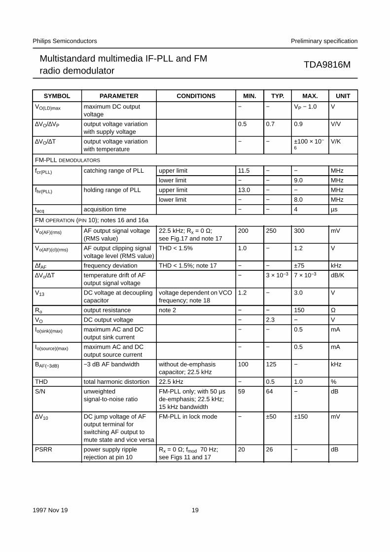
FM-PLL DEMODULATORS
fcr(PLL) catching range of PLL upper limit 11.5 − − MHz
lower limit − − 9.0 MHz
fhr(PLL) holding range of PLL upper limit 13.0 − − MHz
lower limit − − 8.0 MHz
tacq acquisition time − − 4 µs
FM OPERATION (PIN 10); notes 16 and 16a
Vo(AF)(rms) AF output signal voltage(RMS value)
22.5 kHz; Rx = 0 Ω;see Fig.17 and note 17
200 250 300 mV
Vo(AF)(cl)(rms) AF output clipping signalvoltage level (RMS value)
THD < 1.5% 1.0 − 1.2 V
∆fAF frequency deviation THD < 1.5%; note 17 − − ±75 kHz
∆Vo/∆T temperature drift of AFoutput signal voltage
− 3 × 10⁻³ 7 × 10⁻³ dB/K
V13 DC voltage at decouplingcapacitor
voltage dependent on VCOfrequency; note 18
1.2 − 3.0 V
Ro output resistance note 2 − − 150 ΩVO DC output voltage − 2.3 − V
Io(sink)(max) maximum AC and DCoutput sink current
− − 0.5 mA
Io(source)(max) maximum AC and DCoutput source current
− − 0.5 mA
BAF(−3dB) −3 dB AF bandwidth without de-emphasiscapacitor; 22.5 kHz
100 125 − kHz
THD total harmonic distortion 22.5 kHz − 0.5 1.0 %
S/N unweightedsignal-to-noise ratio
FM-PLL only; with 50 µsde-emphasis; 22.5 kHz;15 kHz bandwidth
59 64 − dB
∆V10 DC jump voltage of AFoutput terminal forswitching AF output tomute state and vice versa
FM-PLL in lock mode − ±50 ±150 mV
PSRR power supply ripplerejection at pin 10
Rx = 0 Ω; fmod 70 Hz;see Figs 11 and 17
20 26 − dB
SYMBOL PARAMETER CONDITIONS MIN. TYP. MAX. UNIT

1997 Nov 19 20
Philips Semiconductors Preliminary specification
Multistandard multimedia IF-PLL and FMradio demodulator
TDA9816M
Notes
1. Video and sound parameters are degraded at VP = 4.5 V.
2. This parameter is not tested during production and is only given as application information for designing thetelevision receiver.
3. Loop bandwidth = 70 kHz (natural frequency fn = 12 kHz; damping factor d ≈ 3; calculated for peak level).Resonance circuit of VCO: Q0 > 50; Cext = 8.2 pF ±0.25 pF; Cint ≈ 8.5 pF (loop voltage ≈ 2.7 V).
4. Temperature coefficient of external LC circuit is equal to zero.
5. Vi(IF)(rms) = 10 mV; ∆f = 1 MHz (VCO frequency offset related to picture carrier frequency); white picturevideo modulation.
6. Vi(VIF) signal for nominal video signal.
7. The leakage current of the AGC capacitor should not exceed 1 µA for B/G standard and 10 nA for L standard. Largercurrents will increase the tilt.
8. S/N is the ratio of black-to-white amplitude to the black level noise voltage (RMS value, pin 18). B = 5 MHz weightedin accordance with “CCIR 567”.
9. The intermodulation figures are defined:
; αIM(1.1) value at 1.1 MHz referenced to black/white signal;
; αIM(3.3) value at 3.3 MHz referenced to colour carrier.
MUTE BEHAVIOUR; note 16
αmute(10) forced mute attenuation pin 15 at VP 70 75 − dB
soft mute attenuation RIF level dependent;see Fig.14
20 25 30 dB
I15(forced) forced mute switchingcurrent
α10 > 70 dB − 350 − µA
I15(soft)(dis) current for disabling softmute
α10 > 0 dB − −350 − µA
Vth(11) soft mute thresholdadjustment voltage
Vi(15) = 56 µV 0.8 1.0 1.2 V
Vi(15) = 560 µV 1.2 1.4 1.6 V
tmute time constant mute on or off 3 − 7 ms
Switching levels for logic ports 0 and 1; see also Table 2
Vlogic DC potential for logic 1 orpin not connected
2.8 − VP V
DC potential for logic 0 0 − 0.8 V
IIL LOW-level input current V3,8 = 0 V 50 70 90 µA
Switching levels for logic port 2; see also Table 2 and Fig.14
Vlogic DC potential for logic 1 orpin not connected
0.8 − VP V
DC potential for logic 0 0 − 0.8 V
IIL LOW-level input current V11 = 0 V 110 150 190 µA
SYMBOL PARAMETER CONDITIONS MIN. TYP. MAX. UNIT
αIM 1.1( ) 20V0 at 4.4 MHz
V0 at 1.1 MHz-------------------------------------
3.6dB+log=
αIM 3.3( ) 20V0 at 4.4 MHz
V0 at 3.3 MHz--------------------------------------
log=

1997 Nov 19 21
Philips Semiconductors Preliminary specification
Multistandard multimedia IF-PLL and FMradio demodulator
TDA9816M
10. Measurements taken with SAW filter K3953 (sound carrier suppression: 40 dB); loop bandwidth = 70 kHz.
a) Modulation VSB; sound carrier off; fvideo > 0.5 MHz.
b) Sound carrier on; SIF SAW filter K9453; fvideo = 10 kHz to 10 MHz.
11. Response speed valid for a VIF input level range of 200 µV up to 70 mV.
12. A current source output is provided to match the AFC output signal to different tuning systems. The test circuit isgiven in Fig.7 for TV mode and in Fig.13 for radio mode. The AFC steepness can be changed by the resistors atpin 19.
a) A voltage output is provided to match the AFC output signal to different tuning systems. The DC load currentshould not exceed 180 µA.
13. Depending on the ratio ∆C/C0 of the LC resonant circuit of the VCO (Q0 > 50; see note 3; C0 = Cint + Cext).
14. Source impedance: 2.3 kΩ in parallel with 12 pF (SAW filter); fIF = 38.9 MHz.
15. Without using an SIF SAW filter the mixer can be switched to intercarrier mode by connecting pin 27 and/or pin 28to ground. In this mode the SIF passes the VIF SAW filter and IF intercarrier levels are dependant on the sound shelfof the VIF SAW filter. The intercarrier output signal at pin 14 can be calculated with the following formula using thevideo output signal at pin 18 (Vo(video)(p-p) = 1.1 V typical) as a reference:
with = correction term for RMS value,
= sound-to-picture carrier ratio at VIF input (pins 1 and 2) in dB,
6 dB = correction term of internal circuitry and ±3 dB = tolerance of video output and intercarrier output amplitudeVo(rms).
Example: SAW filter G1962 (sound shelf: 20 dB) ⇒ ⇒ Vo(rms) = 32 mV (typ.).
16. Input level for second IF from an external generator with 50 Ω source impedance. AC-coupled with 10 nF capacitor,fmod = 1 kHz, 27 kHz (54% FM deviation) of audio reference. A VIF/SIF input signal is not permitted. Pins 6 and 5have to be connected to positive supply voltage for minimum IF gain. S/N and THD measurements are taken at50 µs de-emphasis at pin 14 (modulator pre-emphasis has to be activated). The FM demodulator steepness∆Vo(AF)/∆fAF is positive.
a) Second IF input level 10 mV (RMS).
17. Measured with an FM deviation of 27 kHz, the typical AF output signal is 500 mV (RMS) (Rx = 0 Ω). By usingRx = 680 Ω the AF output signal is attenuated by 6 dB (250 mV RMS). For handling a frequency deviation of morethan 53 kHz the AF output signal has to be reduced by using Rx in order to avoid clipping (THD < 1.5%). For anFM deviation up to 100 kHz an attenuation of 6 dB is recommended with Rx = 680 Ω.
18. The leakage current of the decoupling capacitor (2.2 µF) should not exceed 1 µA.
19. For all S/N measurements the used vision IF modulator has to meet the following specifications:
a) Incidental phase modulation for black-to-white jump less than 0.5 degrees.
b) QSS AF performance, measured with the television-demodulator AMF2 (audio output, weighted S/N ratio) betterthan 60 dB (deviation ±27 kHz) for 6 kHz sine wave black-to-white video modulation.
c) Picture-to-sound carrier ratio; PC/SC1 = 13 dB; (transmitter).
Vo rms( ) 1.1 V p p–( ) 1
2 2-----------× 10
Vi SC( )Vi PC( )----------------- dB( ) 6 dB 3 dB±+
20--------------------------------------------------------------------
×=
1
2 2-----------
Vi SC( )Vi PC( )----------------- dB( )
Vi SC( )Vi PC( )----------------- 27 dB–=

1997 Nov 19 22
Philips Semiconductors Preliminary specification
Multistandard multimedia IF-PLL and FMradio demodulator
TDA9816M
20. Measurements taken with SAW filter K3953 for vision and sound IF (suppressed sound carrier) and K9453 forsound IF (suppressed picture carrier). Input level Vi(SIF)(rms) = 10 mV, 27 kHz (54% FM deviation).
21. The PC/SC1 ratio at pins 1 and 2 is calculated as the addition of TV transmitter PC/SC1 ratio and SAW filter PC/SC1ratio. This PC/SC1 ratio is necessary to achieve the S/NW values as noted. A different PC/SC1 ratio will changethese values.
22. Measurements taken with SAW filter G1962 (sound shelf: 20 dB) for vision and sound IF. Pin 27 and/or pin 28 hasto be connected to ground for switching the single reference QSS mixer to intercarrier mode.
23. Measurements taken with SAW filter K9453 (Siemens) for AM sound IF (suppressed picture carrier).
24. The RIF amplifier output (pin 14) has to be connected to a multistandard application ceramic filter for5.5, 6.0 and 10.7 MHz. This total load constitutes an impedance of 250 Ω.
25. d3 tested by using two signals with frequencies of f1 = 10.5 MHz and f2 = 10.7 MHz with a level Vi4(max)(rms) for eachsignal. d3 is the ratio between intermodulation product at 10.3 MHz and output level of Vi4(max)(rms).
26. The control steepness of the radio AFC detector is dependent on the characteristic of the ceramic resonator, pin 24.The figure given here will be obtained when applying a typical resonator of the type CDA 10.7 MC1-A (Murata).The spreading of the control steepness depends on the spreading of the ceramic resonator characteristic(see Fig.13).
Table 1 Input frequencies and carrier ratios
Table 2 Switch logic
DESCRIPTION SYMBOL B/G STANDARD L STANDARDL ACCENTSTANDARD
FMRADIO
UNIT
Picture/IF carrier fPC or fIF 38.9 38.9 33.9 10.7 MHz
Sound carrier fSC1 33.4 32.4 40.4 − MHz
fSC2 33.158 − − − MHz
Picture-to-sound carrier PC/SC1 13 10 10 − dB
PC/SC2 20 − − − dB
FUNCTION LP2 LP1 LP0 REMARKS
Power-down 0 1 0
TV mode B/G standard negativemodulation
0 1 1
L accent standard positivemodulation
0 0 0
L standard 0 0 1
Radio mode AFC soft mute active 1 1 0 RIF level dependent(25 dB)RIF level 1 1 1
AFC forced mute active 1 0 0 forced mute (70 dB)
RIF level 1 0 1

1997 Nov 19 23
Philips Semiconductors Preliminary specification
Multistandard multimedia IF-PLL and FMradio demodulator
TDA9816M
handbook, full pagewidth
4.5
70
1 2.521.5 3 3.5 4 V5 (V)
MHA959
50
600.06
40
0
1
2
0.6
30
206
10
060
−10
gain(dB)
Ituner(mA)Vi(VIF)(rms)
(mV)
(1) (2) (3) (4)
Fig.3 Typical VIF and tuner AGC characteristic.
(1) Ituner; RTOP = 22 kΩ.
(2) Gain.
(3) Ituner; RTOP = 13 kΩ.
(4) Ituner; RTOP = 0 Ω.
handbook, full pagewidth
4.5
80
90
100
110
1 2.521.5 3 3.5 4 V6 (V)
MED862
60
70
50
40
30
20
10
100
1
0.1
0.01
(dBµV)
Vi(SIF)(rms)(mV)
(1) (2)
Fig.4 Typical SIF AGC characteristic.
(1) AM mode.
(2) FM mode.

1997 Nov 19 24
Philips Semiconductors Preliminary specification
Multistandard multimedia IF-PLL and FMradio demodulator
TDA9816M
Fig.5 Typical signal-to-noise ratio as a function ofIF input voltage.
handbook, halfpage
−60 −40 −20 20
70
60
40
20
0
50
30
10
0
0.06 0.6 6 60060
MHA960
S/N(dB)
Vi(VIF)(rms)(dB)
Vi(VIF)(rms)(mV)10
Fig.6 Input signal conditions.
SC = sound carrier, with respect to sync level.
CC = chrominance carrier, with respect to sync level.
PC = picture carrier, with respect to sync level.
The sound carrier levels are taking into accounta sound shelf attenuation of 20 dB (SAW filter G1962).
handbook, halfpage
SC CC PC SC CC PC
BLUE YELLOW
27 dB
13.2 dB
3.2 dB
27 dB
13.2 dB10 dB
MED685 - 1
Fig.7 Measurement conditions and typical AFC characteristic at TV operation.
handbook, full pagewidth
VP = 5 VVP
200
100
0
−200
−100
38.5 38.9 39.3 f (MHz)
(source current)
(sink current)
VAFC(V)
I19(µA)
2.5TDA9816M 19I19
22 kΩ
22 kΩ VAFC100nF
MHA991

1997 Nov 19 25
Philips Semiconductors Preliminary specification
Multistandard multimedia IF-PLL and FMradio demodulator
TDA9816M
Fig.8 Typical video signal levels on output pin 18 (sound carrier off).
handbook, full pagewidth
1.5 V
1.83 V
2.6 V white level
black level
sync level
B/G standard
1.5 V
1.83 V
2.0 V
1.66 V
2.6 V white level
black level
threshold level
threshold level
sync level
L standard MHA992
handbook, halfpage
30
(dB)
50
(2)
(3)
(1)
70 110
10
−10
−30
−50
−7090
Vi (dBµV)
MHA669
Fig.9 Typical audio level, noise and AM rejection(54% FM deviation) for FM (TV).
(1) Signal.
(2) AM rejection.
(3) Noise.
handbook, halfpage
30
(dB)
50
(2)
(3)
(1)
70 110
10
−10
−30
−50
−70
THD(%)
1.6
1.2
0.8
0.4
090
Vi (dBµV)
MHA670
Fig.10 Typical audio level, noise and THD(54% AM modulation) for AM (TV).
(1) Signal.
(2) THD.
(3) Noise.

1997 Nov 19 26
Philips Semiconductors Preliminary specification
Multistandard multimedia IF-PLL and FMradio demodulator
TDA9816M
Fig.11 Ripple rejection condition.
handbook, full pagewidth
TDA9816M
VP = 5 V
t
100 mV (fripple = 70 Hz)
MHA993
VP = 5 V

1997 Nov 19 27
Philips Semiconductors Preliminary specification
Multistandard multimedia IF-PLL and FMradio demodulator
TDA9816M
Fig.12 Front-end level diagram for TV operation.
(1) Depends on TOP.
handbook, full pagewidth
video 1.1 V (p-p)
0.66 × 10⁻³
0.66 × 10⁻⁵
MHA994
20
40
60
80
100
antennainput
(dBµV)
120
10
VHF/UHF tuner VIF VIF amplifier, demodulatorand video
tuner SAW filter TDA9816M
IF signalsRMS value
(V)
10−1
10−2 (TOP)
10−3
10−4
10−5
1
(1)
SAW insertionloss 14 dB
SAW insertionloss 14 dB
tuning gaincontrol range
40 dBRF gain
70 dBVIF AGC
IF slip6 dB

1997 Nov 19 28
Philips Semiconductors Preliminary specification
Multistandard multimedia IF-PLL and FMradio demodulator
TDA9816M
Fig.13 Measurement conditions and typical AFC characteristic at radio operation.
Equivalent compliance C1 = 2.35 pF.
Equivalent mass L1 = 101 µH.
Equivalent resistance R1 = 55 Ω.
Parallel equivalent capacity C0 = 18 pF.
handbook, full pagewidth
50 ∆f (kHz)
VAFC(V)
2.5
0
10.7
MHA995
25
3.0
2.25
3.75
1.5
0.75
045 12565 85 105
Vi(11) (dBµV)
V∆FL(V)
Typical level detector characteristic at radio operation
2-terminal type equivalent circuit of ceramic resonator
C1 L1 R1 (1)
C0
VP = 5 VVP
200
100
0
−200
−100
f (MHz)
(source current)
(sink current)
VAFC(V)
I19(µA)
2.5TDA9816M 19I19
22 kΩ
22 kΩ VAFC100nF

1997 Nov 19 29
Philips Semiconductors Preliminary specification
Multistandard multimedia IF-PLL and FMradio demodulator
TDA9816M
handbook, full pagewidth
125115105
10
−3025 35 75 9565 8555
MHA966
45
−20
−10
0
(1)
(2) (3) (4) (5)
end of level detector range
start of level detector range
Vi(11) (dBµV)
αmute(dB)
Fig.14 Typical audio signal-to-noise ratio as a function of input signal at radio operation.
(4) AF level; R11 = 16 kΩ.
(5) AF level; R11 = 22 kΩ.
(1) AF level; R11 = 0 Ω.
(2) AF level; R11 = 5 kΩ.
(3) AF level; R11 = 11 kΩ.
Fig.15 Typical audio level, S/N ratio and AM rejection (54% FM deviation) for FM (radio).
(1) Signal.
(2) AM rejection.
(3) Noise.
handbook, halfpage
30 50 70
(dB)
110
10
−10
−50
−70
−30
90Vi (dBµV)
MHA967
(1)
(2)
(3)

1997 Nov 19 30
Philips Semiconductors Preliminary specification
Multistandard multimedia IF-PLL and FMradio demodulator
TDA9816M
(1) RF input 102 dBµV (onset of tuner AGC).
(2) RF input 96 dBµV (signal condition for d3 < 60 dB).
(3) RF input 47 dBµV.
Fig.16 Front-end level diagram for radio operation.
handbook, full pagewidth
0
10
20
30
40
50
60
70
90
100
110
80
(1)
(2)
(3)
(dBµV)
−6
−4+13
−6
−4
+62
limite
r
FM
-PLL
MP
X 2
50 m
V
cera
mic
filte
r 2
4 dB
(<6
dB
)
330
Ω m
atch
ing
6 dB
cera
mic
filte
r 1
4 dB
(<6
dB
)
330
Ω m
atch
ing
6 dB
RIF
am
plifi
er+1
3 dB
MHA956
330Ω
330Ω
330 Ω 330 Ω
FM-PLL
V
SFE 10.7 MS2 SFE 10.7 MS2
limiter + FM + AF
+13 dBAF
AGC

1997 Nov 19 31
Philips Semiconductors Preliminary specification
Multistandard multimedia IF-PLL and FMradio demodulator
TDA9816M
INTERNAL CIRCUITRY
Table 3 Equivalent pin circuits and pin voltages
PIN SYMBOLDC VOLTAGE
(V)EQUIVALENT CIRCUIT (WITHOUT ESD PROTECTION CIRCUIT)
1 ViVIF1 3.4
2 ViVIF2 3.4
3 LP0 0 to VP
4 ViRIF 2.7
5 CVAGC 1.5 to 4.0
MHA935
400 µA
+
1
1.1 kΩ
1.1 kΩ
800 Ω
3.4 V
2
400 µA
+
MHA936
2.5 V
60 µA
3
+
60 µA
+
500 Ω
MHA937
2.8 V
500 µA
4
280 Ω 50 Ω
450 Ω 450 Ω
280 Ω+ +
MHA938
52.5 µA
40 µA
1 mA
Ib
0.3/20/40 µA

1997 Nov 19 32
Philips Semiconductors Preliminary specification
Multistandard multimedia IF-PLL and FMradio demodulator
TDA9816M
6 CSAGC 1.5 to 4.0
7 TPLL 1.5 to 4.0
8 LP1 0 to VP
PIN SYMBOLDC VOLTAGE
(V)EQUIVALENT CIRCUIT (WITHOUT ESD PROTECTION CIRCUIT)
MHA998
6
15 µA
+
+ + +
±1 µA
Ib
7
+
200 µA
VCO
Ib
+ ++ +
MHA999
MHB001
8500 Ω
60 µA
60 µA
2.5 V
+
+

1997 Nov 19 33
Philips Semiconductors Preliminary specification
Multistandard multimedia IF-PLL and FMradio demodulator
TDA9816M
9 LADJ 0 to VP
10 VoAF 2.3
11 LP2 0 to 3.0
PIN SYMBOLDC VOLTAGE
(V)EQUIVALENT CIRCUIT (WITHOUT ESD PROTECTION CIRCUIT)
MHB002
+
+
90 µA
1 V 2.5 V
90 µA
9 kΩ 9 kΩ
7.2 kΩ
3.55 V
17 kΩ
7.6 kΩ
9
MHB003
10
++
9 kΩ
30 kΩ
11
++4 µA
MHB004
31 kΩ

1997 Nov 19 34
Philips Semiconductors Preliminary specification
Multistandard multimedia IF-PLL and FMradio demodulator
TDA9816M
12 Cde-em 2.3
13 CDEC 1.2 to 3.0
PIN SYMBOLDC VOLTAGE
(V)EQUIVALENT CIRCUIT (WITHOUT ESD PROTECTION CIRCUIT)
MHB005
12
27.7 kΩ
30 µA
60 µA
30 µA
Ib
+ +
+
+
MHB006
13
++
+
80 µA
Ib

1997 Nov 19 35
Philips Semiconductors Preliminary specification
Multistandard multimedia IF-PLL and FMradio demodulator
TDA9816M
14 VoQSS 2.0
15 ViFM 2.65
16 TAGC 0 to 13.2
PIN SYMBOLDC VOLTAGE
(V)EQUIVALENT CIRCUIT (WITHOUT ESD PROTECTION CIRCUIT)
MHB007
14
1.6 V
2.7 mA
4.7 kΩ
10 pF
12.2kΩ
15.1kΩ
150 kΩ
+
MHB008
15
600 µA
2.67 V
600 Ω 330 Ω
TV radio
MHB009
16
15 V

1997 Nov 19 36
Philips Semiconductors Preliminary specification
Multistandard multimedia IF-PLL and FMradio demodulator
TDA9816M
17 CBL 0 to 3.2
18 Vo(vid) sync level: 1.5
PIN SYMBOLDC VOLTAGE
(V)EQUIVALENT CIRCUIT (WITHOUT ESD PROTECTION CIRCUIT)
MHB010
17
2.5 µA+
5 µA
+
2.5 µA
30 µA
16 µA
2.5 µA
10 µA
+
+ 10 µA
+
0.15 µA+
MHB011
18
3.55 V
3.0 µA 50 kΩ
10 µF
20 kΩ
3.3 kΩ
100 Ω

1997 Nov 19 37
Philips Semiconductors Preliminary specification
Multistandard multimedia IF-PLL and FMradio demodulator
TDA9816M
19 AFC 0.3 to VP − 0.3
20 n.c.
21 VCO1 2.7
22 VCO2 2.7
23 GND
PIN SYMBOLDC VOLTAGE
(V)EQUIVALENT CIRCUIT (WITHOUT ESD PROTECTION CIRCUIT)
MHB012
19
20 kΩ
20 kΩ
LD off
200 µA 5 µA
TV AFC±200 µA
radio LD±200 µA
radioAFC
+ + + +
MHB013
L accent
B/G
2.8 V
20 kΩ
50 Ω420 Ω420 Ω
+ +
20 kΩ
22
21
500 µA
++
MHB014
23
25
10 V

1997 Nov 19 38
Philips Semiconductors Preliminary specification
Multistandard multimedia IF-PLL and FMradio demodulator
TDA9816M
24 CERRES 4.0
25 VP
26 TADJ 0 to 1.9
27 ViSIF1 3.4
28 ViSIF2 3.4
PIN SYMBOLDC VOLTAGE
(V)EQUIVALENT CIRCUIT (WITHOUT ESD PROTECTION CIRCUIT)
+
8.4 kΩ
1 kΩ3 kΩ
MHB015
1 kΩ1 kΩ
5 pF
24
MHB014
23
25
10 V
MHB017
3.55 V20 kΩ
26
30 kΩ
9 kΩ
1.9 V
MHB018
27
QSSWI
28
100 µA
400 µA
2.2 V
12.5 kΩ
+
+
400 µA
+
1 kΩ
800 Ω
1.1 kΩ
1.1 kΩ
3.4 V

1997 Nov 19 39
Philips Semiconductors Preliminary specification
Multistandard multimedia IF-PLL and FMradio demodulator
TDA9816M
TEST AND APPLICATION INFORMATION
ll pagewidth
5
50 Ω
4
3
1 2
1 : 1
inte
rcar
rier
mod
e
VIF
inpu
t
5
50 Ω
4
3
1 2
1 : 1
SIF
inpu
t
RIF
inpu
t
10 n
F33
0 Ω
MH
A99
6
CB
L
100
nF
TV
/rad
iotu
ner
AG
C1.
1 V
(p-
p)vi
deo
1415
5.6
kΩ
5.5
MH
z
560
Ω
10.7
MH
z
330
Ω
10 n
F
QS
S in
terc
arrie
rou
tput
13
72
45
6
2627
2225
2423
89
1011
2120
1918
1217
131628
TD
A98
16M
56 k
Ω
VP
AF
C/R
IFle
vel
33 k
Ω10
0 nF
GN
D
cera
mic
reso
nato
r10
.7 M
Hz
10 n
F8.
2 pF
N15
0
n.c.
Tok
o5
KM
13 kΩ
TO
P
330
Ω
220
nF
2.2
µF
22 µF
22 kΩ
AF
outp
ut
Rx
CD
EC
1.8
nF
SIF
AG
Clo
opfil
ter
LP1
L ac
cent
adju
stde
-em
phas
is
22 k
Ω
6.8
kΩ
LP2
soft
mut
e
LP0
10 nF
2.2
µF
VIF
AG
C
soft
mut
eof
f
forc
edm
ute
switc
h
VP
Fig
.17
Tes
t circ
uit.

1997 Nov 19 40
Philips Semiconductors Preliminary specification
Multistandard multimedia IF-PLL and FMradio demodulator
TDA9816M
, full pagewidth
MH
A99
7
50 Ω
CB
L
100
nF
TV
/rad
iotu
ner
AG
C
1 V
(p-
p)vi
deo
inte
rcar
rier
mod
e
330
Ω15 µH
(1)
(1)
IFin
put
SA
WF
ILT
ER
K94
53
SA
WF
ILT
ER
K39
53
1415
5.6
kΩ
5.5
MH
z
560
Ω
10.7
MH
z
330
Ω
10 n
F
QS
S in
terc
arrie
rou
tput
13
72
45
6
2627
2225
2423
89
1011
2120
1918
1217
131628
TD
A98
16M
56 k
Ω
VP
AF
C/R
IFle
vel
33 k
Ω10
0 nF
GN
D
cera
mic
reso
nato
r10
.7 M
Hz
10 n
F8.
2 pF
N15
0
n.c.
Tok
o5
KM
13 kΩ
TO
P
330
Ω
220
nF
2.2
µF
22 µF
22 kΩ
AF
outp
ut
Rx
CD
EC
1.8
nF
SIF
AG
Clo
opfil
ter
LP1
L ac
cent
adju
stde
-em
phas
is
22 k
Ω
6.8
kΩ
LP2
soft
mut
e
LP0
10 nF
2.2
µF
VIF
AG
C
10.7
MH
z
RIF
inpu
t
270
Ω
soft
mut
eof
f
forc
edm
ute
switc
h
VP
Fig
.18
App
licat
ion
circ
uit.
(1)
Dep
ends
on
stan
dard
.

1997 Nov 19 41
Philips Semiconductors Preliminary specification
Multistandard multimedia IF-PLL and FMradio demodulator
TDA9816M
PACKAGE OUTLINE
UNIT A1 A2 A3 bp c D(1) E(1) (1)e HE L Lp Q Zywv θ
REFERENCESOUTLINEVERSION
EUROPEANPROJECTION ISSUE DATE
IEC JEDEC EIAJ
mm 0.210.05
1.801.65
0.380.25
0.200.09
10.410.0
5.45.2 0.65 1.25
7.97.6
0.90.7
1.10.7
80
o
o0.13 0.10.2
DIMENSIONS (mm are the original dimensions)
Note
1. Plastic or metal protrusions of 0.20 mm maximum per side are not included.
1.030.63
SOT341-1 MO-150AH93-09-0895-02-04
X
w M
θ
AA1
A2
bp
D
HE
Lp
Q
detail X
E
Z
e
c
L
v M A
(A )3
A
1 14
28 15
0.25
y
pin 1 index
0 2.5 5 mm
scale
SSOP28: plastic shrink small outline package; 28 leads; body width 5.3 mm SOT341-1
Amax.
2.0

1997 Nov 19 42
Philips Semiconductors Preliminary specification
Multistandard multimedia IF-PLL and FMradio demodulator
TDA9816M
SOLDERING
Introduction
There is no soldering method that is ideal for all ICpackages. Wave soldering is often preferred whenthrough-hole and surface mounted components are mixedon one printed-circuit board. However, wave soldering isnot always suitable for surface mounted ICs, or forprinted-circuits with high population densities. In thesesituations reflow soldering is often used.
This text gives a very brief insight to a complex technology.A more in-depth account of soldering ICs can be found inour “IC Package Databook” (order code 9398 652 90011).
Reflow soldering
Reflow soldering techniques are suitable for all SSOPpackages.
Reflow soldering requires solder paste (a suspension offine solder particles, flux and binding agent) to be appliedto the printed-circuit board by screen printing, stencilling orpressure-syringe dispensing before package placement.
Several techniques exist for reflowing; for example,thermal conduction by heated belt. Dwell times varybetween 50 and 300 seconds depending on heatingmethod. Typical reflow temperatures range from215 to 250 °C.
Preheating is necessary to dry the paste and evaporatethe binding agent. Preheating duration: 45 minutes at45 °C.
Wave soldering
Wave soldering is not recommended for SSOP packages.This is because of the likelihood of solder bridging due toclosely-spaced leads and the possibility of incompletesolder penetration in multi-lead devices.
If wave soldering cannot be avoided, the followingconditions must be observed:
• A double-wave (a turbulent wave with high upwardpressure followed by a smooth laminar wave)soldering technique should be used.
• The longitudinal axis of the package footprint mustbe parallel to the solder flow and must incorporatesolder thieves at the downstream end.
Even with these conditions, only consider wavesoldering SSOP packages that have a body width of4.4 mm, that is SSOP16 (SOT369-1) orSSOP20 (SOT266-1).
During placement and before soldering, the package mustbe fixed with a droplet of adhesive. The adhesive can beapplied by screen printing, pin transfer or syringedispensing. The package can be soldered after theadhesive is cured.
Maximum permissible solder temperature is 260 °C, andmaximum duration of package immersion in solder is10 seconds, if cooled to less than 150 °C within6 seconds. Typical dwell time is 4 seconds at 250 °C.
A mildly-activated flux will eliminate the need for removalof corrosive residues in most applications.
Repairing soldered joints
Fix the component by first soldering two diagonally-opposite end leads. Use only a low voltage soldering iron(less than 24 V) applied to the flat part of the lead. Contacttime must be limited to 10 seconds at up to 300 °C. Whenusing a dedicated tool, all other leads can be soldered inone operation within 2 to 5 seconds between270 and 320 °C.

1997 Nov 19 43
Philips Semiconductors Preliminary specification
Multistandard multimedia IF-PLL and FMradio demodulator
TDA9816M
DEFINITIONS
LIFE SUPPORT APPLICATIONS
These products are not designed for use in life support appliances, devices, or systems where malfunction of theseproducts can reasonably be expected to result in personal injury. Philips customers using or selling these products foruse in such applications do so at their own risk and agree to fully indemnify Philips for any damages resulting from suchimproper use or sale.
Data sheet status
Objective specification This data sheet contains target or goal specifications for product development.
Preliminary specification This data sheet contains preliminary data; supplementary data may be published later.
Product specification This data sheet contains final product specifications.
Limiting values
Limiting values given are in accordance with the Absolute Maximum Rating System (IEC 134). Stress above one ormore of the limiting values may cause permanent damage to the device. These are stress ratings only and operationof the device at these or at any other conditions above those given in the Characteristics sections of the specificationis not implied. Exposure to limiting values for extended periods may affect device reliability.
Application information
Where application information is given, it is advisory and does not form part of the specification.

Internet: http://www.semiconductors.philips.com
Philips Semiconductors – a worldwide company
© Philips Electronics N.V. 1997 SCA56
All rights are reserved. Reproduction in whole or in part is prohibited without the prior written consent of the copyright owner.
The information presented in this document does not form part of any quotation or contract, is believed to be accurate and reliable and may be changedwithout notice. No liability will be accepted by the publisher for any consequence of its use. Publication thereof does not convey nor imply any licenseunder patent- or other industrial or intellectual property rights.
Netherlands: Postbus 90050, 5600 PB EINDHOVEN, Bldg. VB,Tel. +31 40 27 82785, Fax. +31 40 27 88399
New Zealand: 2 Wagener Place, C.P.O. Box 1041, AUCKLAND,Tel. +64 9 849 4160, Fax. +64 9 849 7811
Norway: Box 1, Manglerud 0612, OSLO,Tel. +47 22 74 8000, Fax. +47 22 74 8341
Philippines: Philips Semiconductors Philippines Inc.,106 Valero St. Salcedo Village, P.O. Box 2108 MCC, MAKATI,Metro MANILA, Tel. +63 2 816 6380, Fax. +63 2 817 3474
Poland: Ul. Lukiska 10, PL 04-123 WARSZAWA,Tel. +48 22 612 2831, Fax. +48 22 612 2327
Portugal: see Spain
Romania: see Italy
Russia: Philips Russia, Ul. Usatcheva 35A, 119048 MOSCOW,Tel. +7 095 755 6918, Fax. +7 095 755 6919
Singapore: Lorong 1, Toa Payoh, SINGAPORE 1231,Tel. +65 350 2538, Fax. +65 251 6500
Slovakia: see Austria
Slovenia: see Italy
South Africa: S.A. PHILIPS Pty Ltd., 195-215 Main Road Martindale,2092 JOHANNESBURG, P.O. Box 7430 Johannesburg 2000,Tel. +27 11 470 5911, Fax. +27 11 470 5494
South America: Al. Vicente Pinzon, 173, 6th floor,04547-130 SÃO PAULO, SP, Brazil,Tel. +55 11 821 2333, Fax. +55 11 821 2382
Spain: Balmes 22, 08007 BARCELONA,Tel. +34 3 301 6312, Fax. +34 3 301 4107
Sweden: Kottbygatan 7, Akalla, S-16485 STOCKHOLM,Tel. +46 8 632 2000, Fax. +46 8 632 2745
Switzerland: Allmendstrasse 140, CH-8027 ZÜRICH,Tel. +41 1 488 2686, Fax. +41 1 481 7730
Taiwan: Philips Semiconductors, 6F, No. 96, Chien Kuo N. Rd., Sec. 1,TAIPEI, Taiwan Tel. +886 2 2134 2865, Fax. +886 2 2134 2874
Thailand: PHILIPS ELECTRONICS (THAILAND) Ltd.,209/2 Sanpavuth-Bangna Road Prakanong, BANGKOK 10260,Tel. +66 2 745 4090, Fax. +66 2 398 0793
Turkey: Talatpasa Cad. No. 5, 80640 GÜLTEPE/ISTANBUL,Tel. +90 212 279 2770, Fax. +90 212 282 6707
Ukraine : PHILIPS UKRAINE, 4 Patrice Lumumba str., Building B, Floor 7,252042 KIEV, Tel. +380 44 264 2776, Fax. +380 44 268 0461
United Kingdom: Philips Semiconductors Ltd., 276 Bath Road, Hayes,MIDDLESEX UB3 5BX, Tel. +44 181 730 5000, Fax. +44 181 754 8421
United States: 811 East Arques Avenue, SUNNYVALE, CA 94088-3409,Tel. +1 800 234 7381
Uruguay: see South America
Vietnam: see Singapore
Yugoslavia: PHILIPS, Trg N. Pasica 5/v, 11000 BEOGRAD,Tel. +381 11 625 344, Fax.+381 11 635 777
For all other countries apply to: Philips Semiconductors,International Marketing & Sales Communications, Building BE-p,P.O. Box 218, 5600 MD EINDHOVEN, The Netherlands, Fax. +31 40 27 24825
Argentina: see South America
Australia: 34 Waterloo Road, NORTH RYDE, NSW 2113,Tel. +61 2 9805 4455, Fax. +61 2 9805 4466
Austria: Computerstr. 6, A-1101 WIEN, P.O. Box 213, Tel. +43 160 1010,Fax. +43 160 101 1210
Belarus: Hotel Minsk Business Center, Bld. 3, r. 1211, Volodarski Str. 6,220050 MINSK, Tel. +375 172 200 733, Fax. +375 172 200 773
Belgium: see The Netherlands
Brazil: see South America
Bulgaria: Philips Bulgaria Ltd., Energoproject, 15th floor,51 James Bourchier Blvd., 1407 SOFIA,Tel. +359 2 689 211, Fax. +359 2 689 102
Canada: PHILIPS SEMICONDUCTORS/COMPONENTS,Tel. +1 800 234 7381
China/Hong Kong: 501 Hong Kong Industrial Technology Centre,72 Tat Chee Avenue, Kowloon Tong, HONG KONG,Tel. +852 2319 7888, Fax. +852 2319 7700
Colombia: see South America
Czech Republic: see Austria
Denmark: Prags Boulevard 80, PB 1919, DK-2300 COPENHAGEN S,Tel. +45 32 88 2636, Fax. +45 31 57 0044
Finland: Sinikalliontie 3, FIN-02630 ESPOO,Tel. +358 9 615800, Fax. +358 9 61580920
France: 51 Rue Carnot, BP317, 92156 SURESNES Cedex,Tel. +33 1 40 99 6161, Fax. +33 1 40 99 6427
Germany: Hammerbrookstraße 69, D-20097 HAMBURG,Tel. +49 40 23 53 60, Fax. +49 40 23 536 300
Greece: No. 15, 25th March Street, GR 17778 TAVROS/ATHENS,Tel. +30 1 4894 339/239, Fax. +30 1 4814 240
Hungary: see Austria
India: Philips INDIA Ltd, Band Box Building, 2nd floor,254-D, Dr. Annie Besant Road, Worli, MUMBAI 400 025,Tel. +91 22 493 8541, Fax. +91 22 493 0966
Indonesia: see Singapore
Ireland: Newstead, Clonskeagh, DUBLIN 14,Tel. +353 1 7640 000, Fax. +353 1 7640 200
Israel: RAPAC Electronics, 7 Kehilat Saloniki St, PO Box 18053,TEL AVIV 61180, Tel. +972 3 645 0444, Fax. +972 3 649 1007
Italy: PHILIPS SEMICONDUCTORS, Piazza IV Novembre 3,20124 MILANO, Tel. +39 2 6752 2531, Fax. +39 2 6752 2557
Japan: Philips Bldg 13-37, Kohnan 2-chome, Minato-ku, TOKYO 108,Tel. +81 3 3740 5130, Fax. +81 3 3740 5077
Korea: Philips House, 260-199 Itaewon-dong, Yongsan-ku, SEOUL,Tel. +82 2 709 1412, Fax. +82 2 709 1415
Malaysia: No. 76 Jalan Universiti, 46200 PETALING JAYA, SELANGOR,Tel. +60 3 750 5214, Fax. +60 3 757 4880
Mexico: 5900 Gateway East, Suite 200, EL PASO, TEXAS 79905,Tel. +9-5 800 234 7381
Middle East: see Italy
Printed in The Netherlands 547047/1200/01/pp44 Date of release: 1997 Nov 19 Document order number: 9397 750 02596