Embed Size (px)
Citation preview
© 2004 Pearson Education, Inc.M. Morris Mano & Charles R. KimeLOGIC AND COMPUTER DESIGN FUNDAMENTALS, 3e
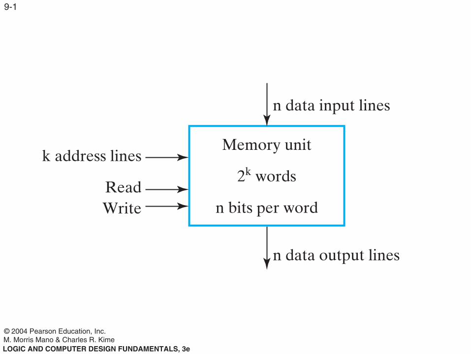
9-1
k address lines
Read
Memory unit
2k words
n bits per word
n data input lines
n data output lines
Write
© 2004 Pearson Education, Inc.M. Morris Mano & Charles R. KimeLOGIC AND COMPUTER DESIGN FUNDAMENTALS, 3e
9-2
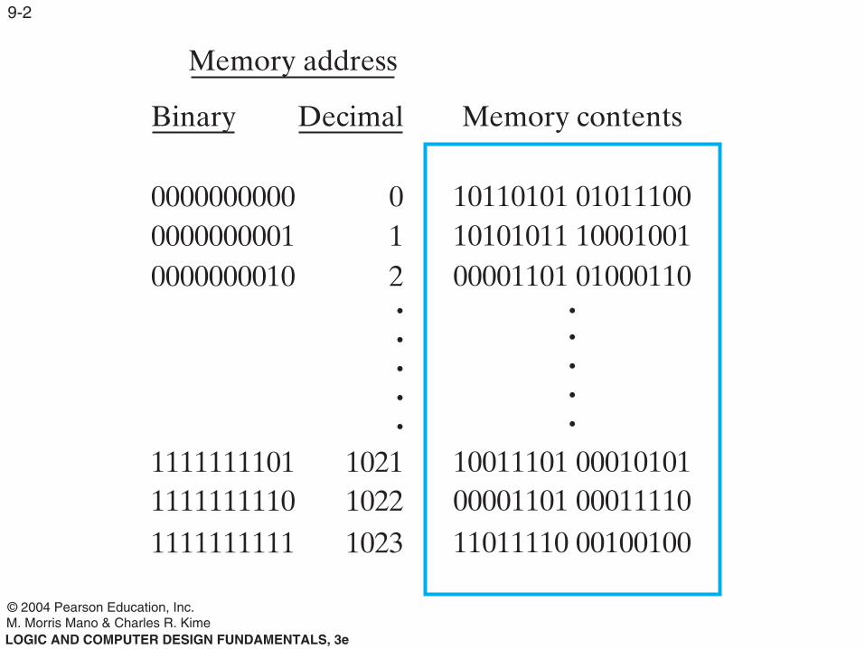
Memory address
Binary
000000000000000000010000000010
111111110111111111101111111111
Memory contents
10110101 0101110010101011 1000100100001101 01000110
10011101 0001010100001101 0001111011011110 00100100
.
.
.
.
.
Decimal
012
102110221023
.
.
.
.
.
© 2004 Pearson Education, Inc.M. Morris Mano & Charles R. KimeLOGIC AND COMPUTER DESIGN FUNDAMENTALS, 3e
T 9-1
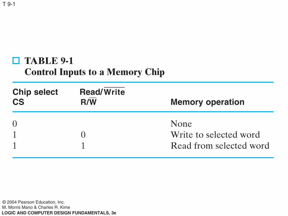
TABLE 9-1Control Inputs to a Memory Chip
Chip selectCS
Read/Memory operation
011
�01
NoneWrite to selected wordRead from selected word
WriteR/W
© 2004 Pearson Education, Inc.M. Morris Mano & Charles R. KimeLOGIC AND COMPUTER DESIGN FUNDAMENTALS, 3e
9-3
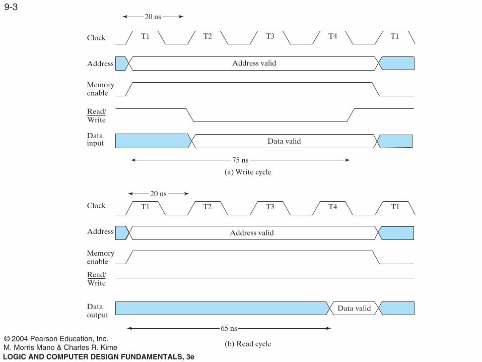
(a) Write cycle
Clock
Address
Memoryenable
Read/Write
Datainput
20 ns
T1 T2 T3 T4 T1
Address valid
Data valid
75 ns
(b) Read cycle
Clock
Address
Memoryenable
Read/Write
Dataoutput
20 ns
T1 T2 T3 T4 T1
Address valid
65 ns
Data valid
© 2004 Pearson Education, Inc.M. Morris Mano & Charles R. KimeLOGIC AND COMPUTER DESIGN FUNDAMENTALS, 3e
9-4
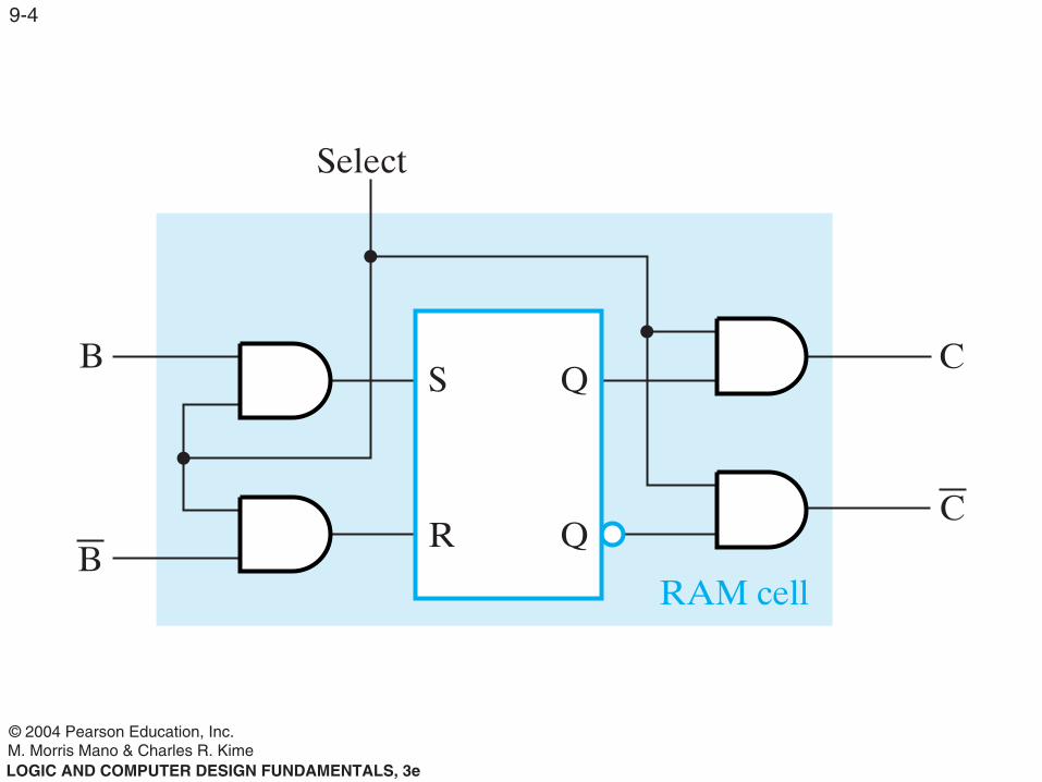
Select
B
RAM cell
C
C
B
S
R
Q
Q
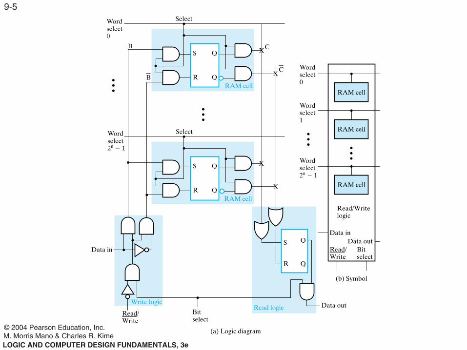
© 2004 Pearson Education, Inc.M. Morris Mano & Charles R. KimeLOGIC AND COMPUTER DESIGN FUNDAMENTALS, 3e
9-5
(a) Logic diagram
Select
S
R
Q
Q
B
RAM cell
C
CB
Select
S
R
Q
QRAM cell
X
Wordselect0
Wordselect2n 2 1
Data in
Write logic
Read/Write
Bitselect
S
R
Q
Q
X
X
XWordselect0
Wordselect1
Wordselect2n 2 1
Read/Writelogic
Data inData out
Read/Write
Bitselect
(b) Symbol
RAM cell
RAM cell
RAM cell
Data outRead logic
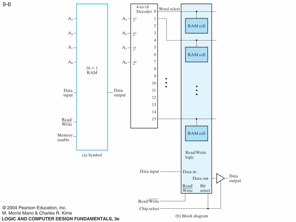
© 2004 Pearson Education, Inc.M. Morris Mano & Charles R. KimeLOGIC AND COMPUTER DESIGN FUNDAMENTALS, 3e
9-6Word select
Read/Writelogic
Data in
Data out
Read/Write
Bitselect
(b) Block diagram
RAM cell
RAM cell
RAM cell
Data input
Chip select
Read/Write
Dataoutput
A3
A2
A1
A0
23
22
21
20
4-to-16Decoder 0
1
2
3
4
5
6
7
8
9
10
11
12
13
14
15
A3
A2
A1
A0
Datainput
Dataoutput
(a) Symbol
Read/Write
Memoryenable
16 3 1RAM
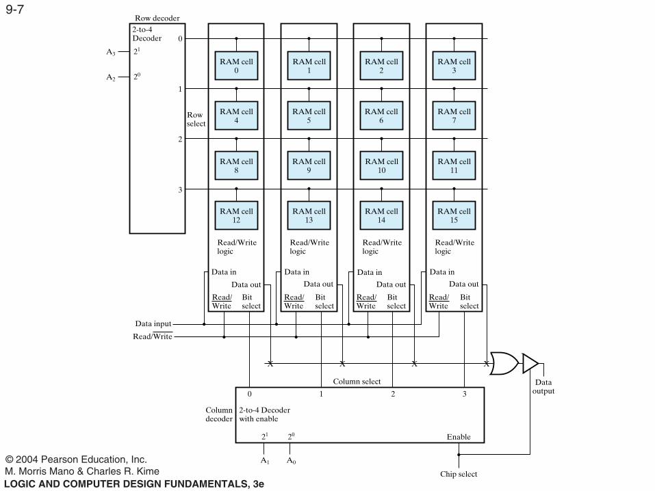
© 2004 Pearson Education, Inc.M. Morris Mano & Charles R. KimeLOGIC AND COMPUTER DESIGN FUNDAMENTALS, 3e
9-7
Data input
Read/Write
X XX
A1 A0
RAM cell0
RAM cell4
RAM cell8
RAM cell12
Read/Writelogic
Data in
Data out
Read/Write
Bitselect
RAM cell1
RAM cell5
RAM cell9
RAM cell13
Read/Writelogic
Data in
Data out
Read/Write
Bitselect
RAM cell2
RAM cell6
RAM cell10
RAM cell14
Read/Writelogic
Data in
Data out
Read/Write
Bitselect
RAM cell3
RAM cell7
RAM cell11
RAM cell15
Read/Writelogic
Data in
Data out
Read/Write
Bitselect
Columndecoder
2-to-4 Decoderwith enable
21 20
0 1
Column select
2
Enable
3
Chip select
Dataoutput
Rowselect
Row decoder
A2
A3
X
2-to-4Decoder
20
21
1
2
3
0
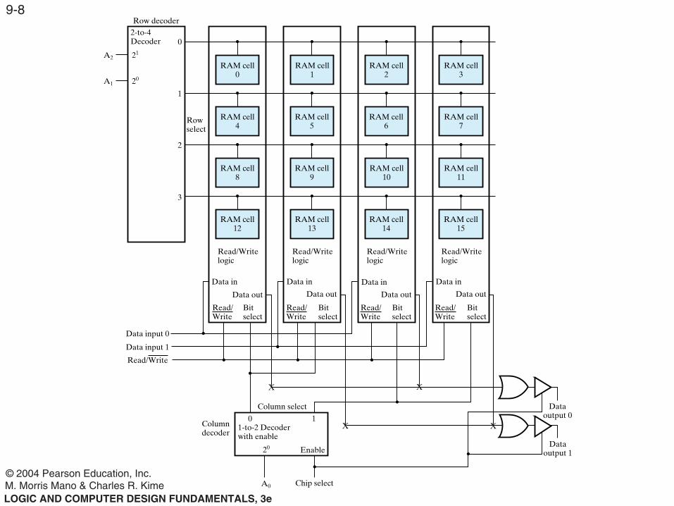
© 2004 Pearson Education, Inc.M. Morris Mano & Charles R. KimeLOGIC AND COMPUTER DESIGN FUNDAMENTALS, 3e
9-8
A0 Chip select
Data input 0
X
X
X
Columndecoder
1-to-2 Decoderwith enable
20
0
Column select Dataoutput 0
X
EnableData
output 1
Data input 1
Read/Write
1
RAM cell0
RAM cell4
RAM cell8
RAM cell12
Read/Writelogic
Data in
Data out
Read/Write
Bitselect
RAM cell1
RAM cell5
RAM cell9
RAM cell13
Read/Writelogic
Data in
Data out
Read/Write
Bitselect
RAM cell2
RAM cell6
RAM cell10
RAM cell14
Read/Writelogic
Data in
Data out
Read/Write
Bitselect
RAM cell3
RAM cell7
RAM cell11
RAM cell15
Read/Writelogic
Data in
Data out
Read/Write
Bitselect
Rowselect
Row decoder
A1
A2
2-to-4Decoder
20
21
1
2
3
0
© 2004 Pearson Education, Inc.M. Morris Mano & Charles R. KimeLOGIC AND COMPUTER DESIGN FUNDAMENTALS, 3e
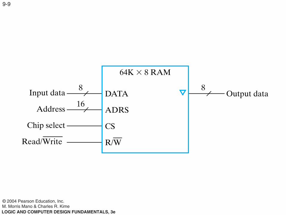
9-9
Input data
Address
Chip select
Output data8
16DATA
ADRS
CS
8
64K 3 8 RAM
Read/Write R/W
© 2004 Pearson Education, Inc.M. Morris Mano & Charles R. KimeLOGIC AND COMPUTER DESIGN FUNDAMENTALS, 3e
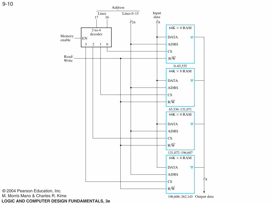
9-10
Inputdata
DATA
Address
ADRS
CS
Output data
8
8
64K 3 8 RAM
Read/Write R/W
Memoryenable
DATA
ADRS
CS
64K 3 8 RAM
DATA
ADRS
CS
64K 3 8 RAM
DATA
ADRS
CS
64K 3 8 RAM
Lines Lines 0–1517 16
2-to-4decoder
EN
0123
16
0–65,535
65,536–131,071
131,072–196,607
196,608–262,143
R/W
R/W
R/W
© 2004 Pearson Education, Inc.M. Morris Mano & Charles R. KimeLOGIC AND COMPUTER DESIGN FUNDAMENTALS, 3e
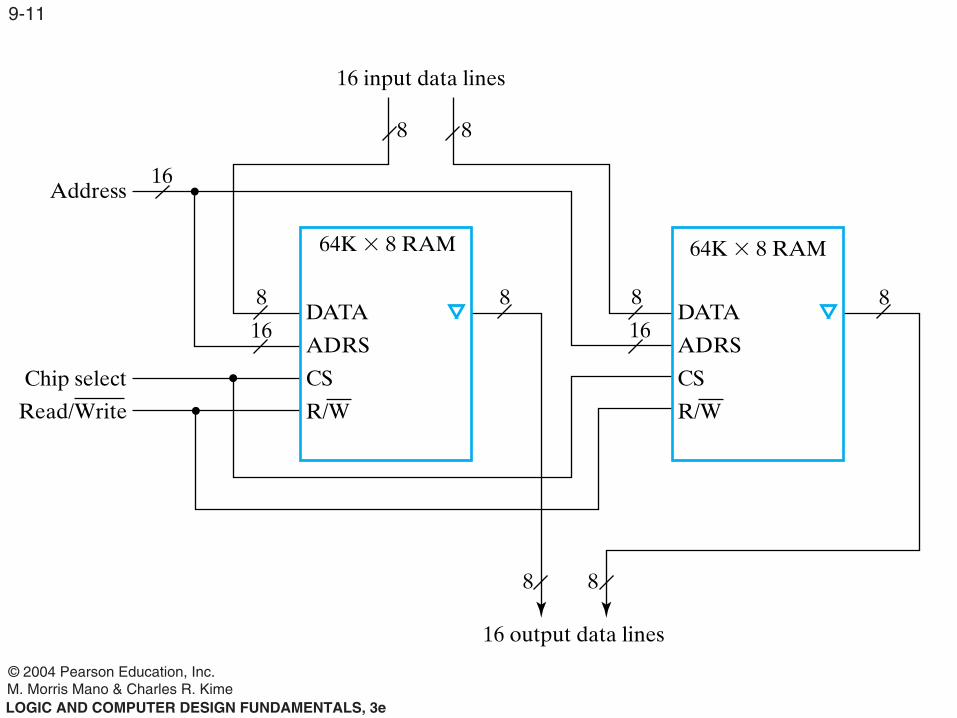
9-11
8
8
8
16
16DATA
ADRS
CS
64K 3 8 RAM
DATA
ADRS
CS
64K 3 8 RAM
8
16 input data lines
8
Address
Chip select
16 output data lines
16
R/WR/WRead/Write
8
8
8
© 2004 Pearson Education, Inc.M. Morris Mano & Charles R. KimeLOGIC AND COMPUTER DESIGN FUNDAMENTALS, 3e
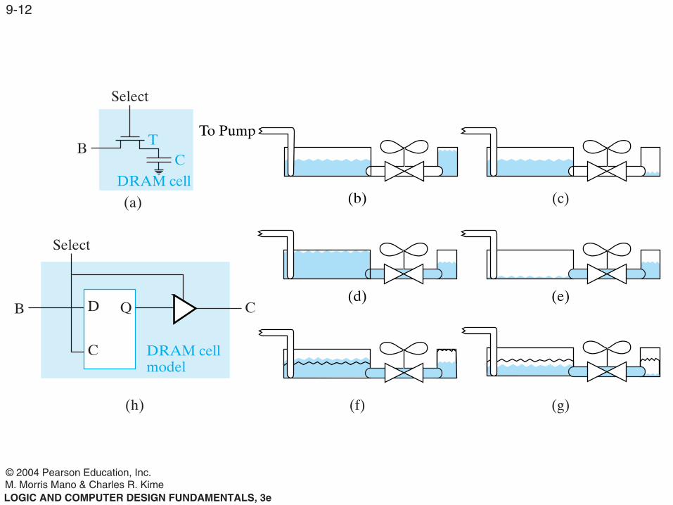
9-12
(a) (c)
Select
D
C
QB
DRAM cellmodel
C
(f) (g)(h)
Select
BT
CDRAM cell
To Pump
(b)
(d) (e)
© 2004 Pearson Education, Inc.M. Morris Mano & Charles R. KimeLOGIC AND COMPUTER DESIGN FUNDAMENTALS, 3e
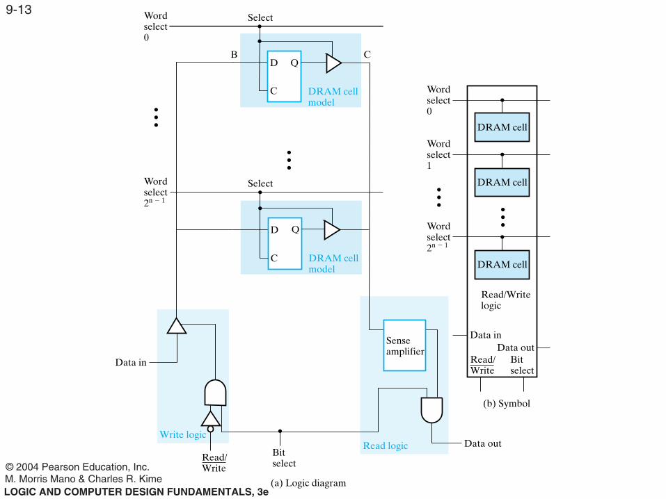
9-13
(b) Symbol
(a) Logic diagram
Select
B
Select
Word�select�0
Word�select�2n 2 1
Data in
Write logic
Bit�select
Data outRead logic
D
C
Q
DRAM cellmodel
D
C
Q
DRAM cellmodel
C
Senseamplifier
Read/Write�logic
Data inData out
Bit�select
DRAM cell
DRAM cell
DRAM cell
Word�select�0
Word�select�1
Word�select�2n 2 1
Read/�Write
Read/�Write
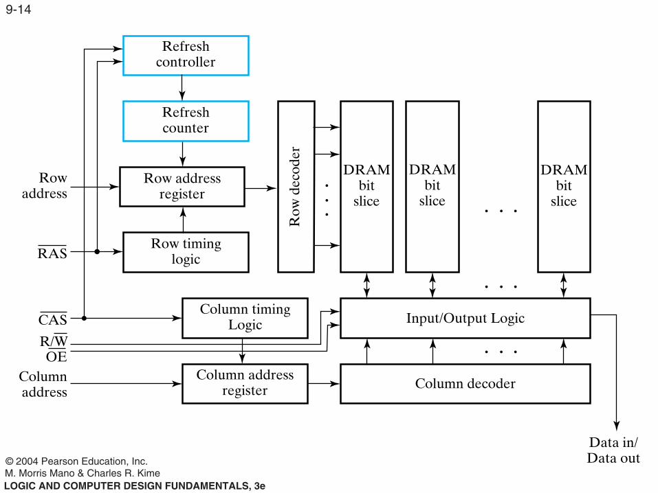
© 2004 Pearson Education, Inc.M. Morris Mano & Charles R. KimeLOGIC AND COMPUTER DESIGN FUNDAMENTALS, 3e
9-14
DRAMbit
slice
DRAMbit
slice
DRAMbit
slice
Input/Output Logic
Column decoder
Row
dec
oder
Column addressregister
Column timingLogic
Row addressregister
Refreshcounter
Refreshcontroller
Row timinglogic
•
Data in/�Data out
RAS
CAS
OER/W
Rowaddress
Columnaddress
.
.
. . . .
. . .
. . .
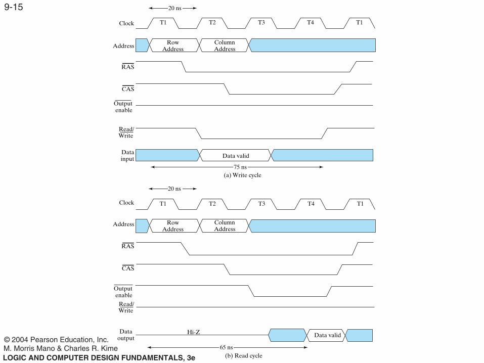
© 2004 Pearson Education, Inc.M. Morris Mano & Charles R. KimeLOGIC AND COMPUTER DESIGN FUNDAMENTALS, 3e
9-15
(a) Write cycle
20 ns
T1 T2 T3 T4 T1
Data valid
75 ns
Read/Write
Datainput
Clock
RowAddress
ColumnAddress
RAS
CAS
Address
Outputenable
(b) Read cycle
20 ns
T1 T2 T3 T4 T1
Data valid
65 ns
Hi-Z
Read/Write
Dataoutput
Clock
RowAddress
ColumnAddress
RAS
CAS
Address
Outputenable
© 2004 Pearson Education, Inc.M. Morris Mano & Charles R. KimeLOGIC AND COMPUTER DESIGN FUNDAMENTALS, 3e
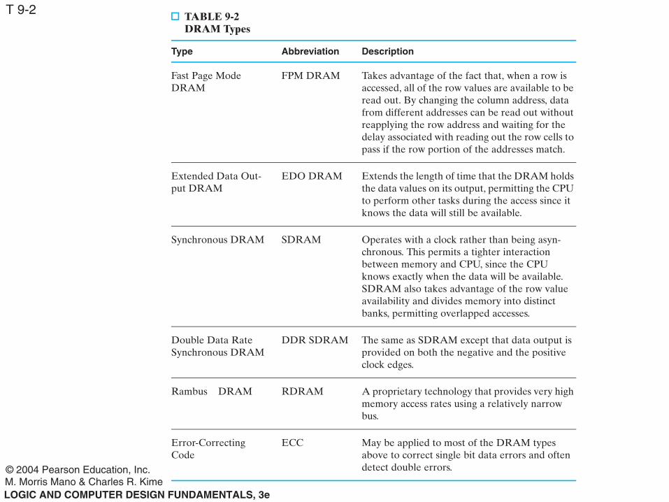
T 9-2 TABLE 9-2DRAM Types
Type Abbreviation Description
Fast Page Mode DRAM
FPM DRAM Takes advantage of the fact that, when a row is accessed, all of the row values are available to be read out. By changing the column address, data from different addresses can be read out without reapplying the row address and waiting for the delay associated with reading out the row cells to pass if the row portion of the addresses match.
Extended Data Out-put DRAM
EDO DRAM Extends the length of time that the DRAM holds the data values on its output, permitting the CPU to perform other tasks during the access since it knows the data will still be available.
Synchronous DRAM SDRAM Operates with a clock rather than being asyn-chronous. This permits a tighter interaction between memory and CPU, since the CPU knows exactly when the data will be available. SDRAM also takes advantage of the row value availability and divides memory into distinct banks, permitting overlapped accesses.
Double Data Rate Synchronous DRAM
DDR SDRAM The same as SDRAM except that data output is provided on both the negative and the positive clock edges.
Rambus� DRAM RDRAM A proprietary technology that provides very high memory access rates using a relatively narrow bus.
Error-Correcting Code
ECC May be applied to most of the DRAM types above to correct single bit data errors and often detect double errors.
© 2004 Pearson Education, Inc.M. Morris Mano & Charles R. KimeLOGIC AND COMPUTER DESIGN FUNDAMENTALS, 3e
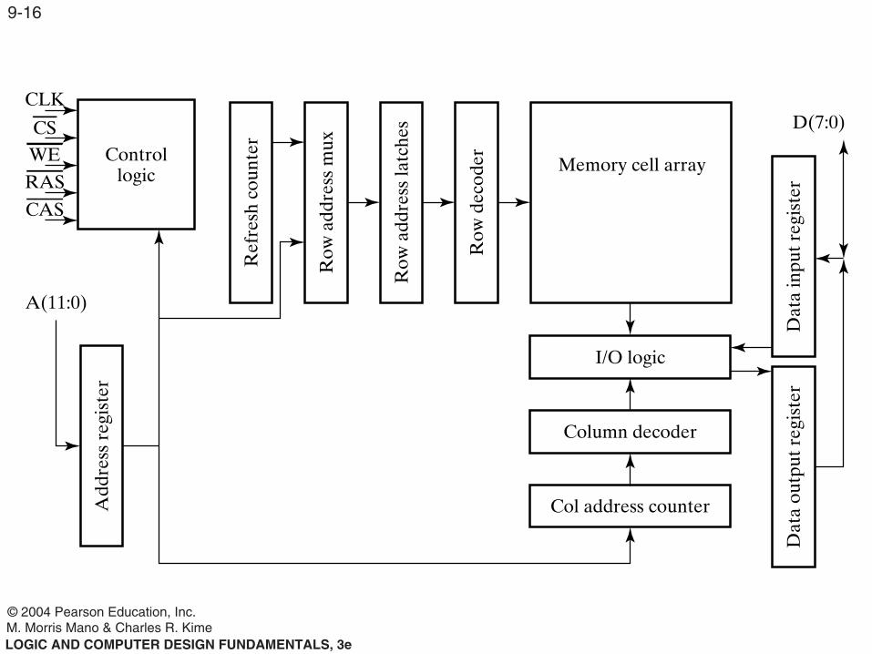
9-16
Memory cell arrayControllogic
I/O logic
Add
ress
reg
iste
r
Ref
resh
cou
nter
Row
add
ress
mux
Row
add
ress
latc
hes
Row
dec
oder
Dat
a in
put r
egis
ter
Dat
a ou
tput
reg
iste
r
Column decoder
Col address counter
CLK
CSWE
RAS
CAS
A(11:0)
D(7:0)
© 2004 Pearson Education, Inc.M. Morris Mano & Charles R. KimeLOGIC AND COMPUTER DESIGN FUNDAMENTALS, 3e
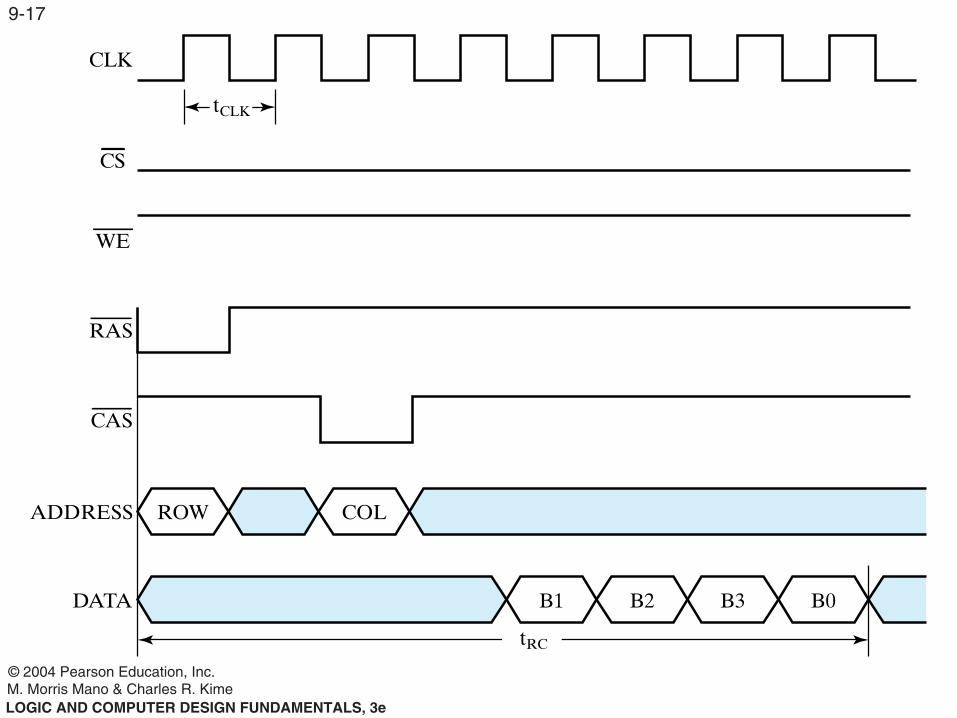
9-17
CLK
CS
WE
RAS
CAS
ADDRESS
DATA
ROW COL
B1 B2 B3 B0
tRC
tCLK
© 2004 Pearson Education, Inc.M. Morris Mano & Charles R. KimeLOGIC AND COMPUTER DESIGN FUNDAMENTALS, 3e
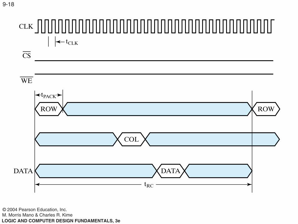
9-18
CLK
CS
WE
DATA
ROW ROW
COL
DATA
tCLK
tPACK
tRC