Embed Size (px)
Citation preview
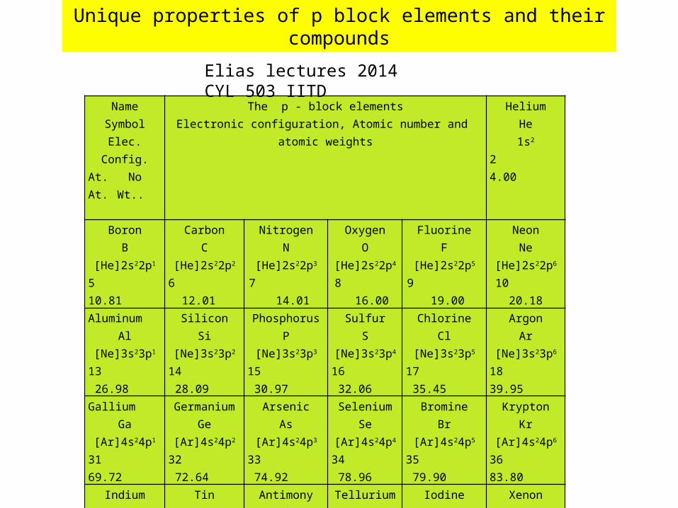
NameSymbol
Elec. Config.At. No At. Wt..
The p - block elementsElectronic configuration, Atomic number and atomic
weights
HeliumHe1s2
2 4.00
BoronB
[He]2s22p1
5 10.81
CarbonC
[He]2s22p2
6 12.01
NitrogenN
[He]2s22p3
7 14.01
OxygenO
[He]2s22p4
8 16.00
FluorineF
[He]2s22p5
9 19.00
NeonNe
[He]2s22p6
10 20.18
AluminumAl
[Ne]3s23p1
13 26.98
SiliconSi
[Ne]3s23p2
14 28.09
PhosphorusP
[Ne]3s23p3
15 30.97
SulfurS
[Ne]3s23p4
16 32.06
ChlorineCl
[Ne]3s23p5
17 35.45
ArgonAr
[Ne]3s23p6
18 39.95
GalliumGa
[Ar]4s24p1
31 69.72
GermaniumGe
[Ar]4s24p2
32 72.64
ArsenicAs
[Ar]4s24p3
33 74.92
SeleniumSe
[Ar]4s24p4
34 78.96
BromineBr
[Ar]4s24p5
35 79.90
KryptonKr
[Ar]4s24p6
36 83.80
IndiumIn
[Kr]5s25p1
49 114.82
TinSn
[Kr]5s25p2
50 118.71
AntimonySb
[Kr]5s25p3
51 121.76
TelluriumTe
[Kr]5s25p4
52 127.60
IodineI
[Kr]5s25p5
53 126.90
XenonXe
[Kr]5s25p6
54 131.29
ThalliumTl
[Xe]6s26p1
81 204.38
LeadPb
[Xe]6s26p2
82 207.20
BismuthBi
[Xe]6s26p3
83 208.98
PoloniumPo
[Xe]6s26p4
84 209
AstatineAt
[Xe]6s26p5
85 210
RadonRn
[Xe]6s26p6
86 222
Unique properties of p block elements and their compounds
Elias lectures 2014 CYL 503 IITD
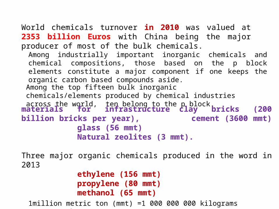
World chemicals turnover in 2010 was valued at 2353 billion Euros with China being the major producer of most of the bulk chemicals.
Among industrially important inorganic chemicals and chemical compositions, those based on the p block elements constitute a major component if one keeps the organic carbon based compounds aside.
Among the top fifteen bulk inorganic chemicals/elements produced by chemical industries across the world, ten belong to the p block.
materials for infrastructure clay bricks (200 billion bricks per year), cement (3600 mmt) glass (56 mmt) Natural zeolites (3 mmt).
Three major organic chemicals produced in the word in 2013 ethylene (156 mmt) propylene (80 mmt) methanol (65 mmt)
1million metric ton (mmt) =1 000 000 000 kilograms (10 crore kg!)
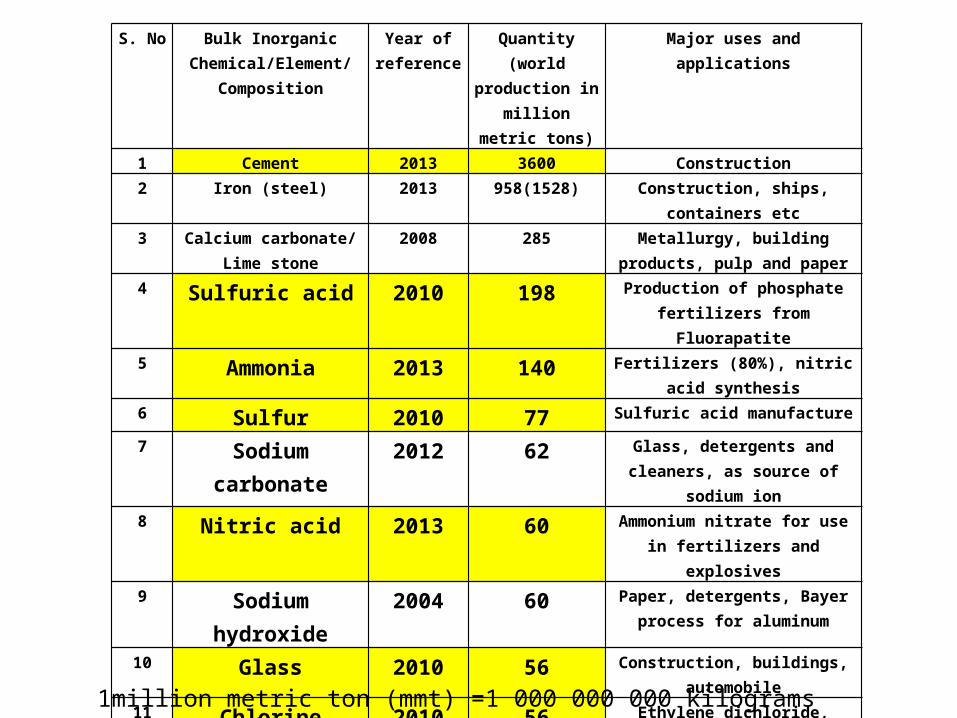
S. No Bulk Inorganic Chemical/Element/
Composition
Year of reference
Quantity(world production in million metric
tons)
Major uses and applications
1 Cement 2013 3600 Construction2 Iron (steel) 2013 958(1528) Construction, ships, containers etc3 Calcium carbonate/
Lime stone2008 285 Metallurgy, building products, pulp
and paper4 Sulfuric acid 2010 198 Production of phosphate fertilizers
from Fluorapatite5 Ammonia 2013 140 Fertilizers (80%), nitric acid
synthesis6 Sulfur 2010 77 Sulfuric acid manufacture
7 Sodium carbonate 2012 62 Glass, detergents and cleaners, as source of sodium ion
8 Nitric acid 2013 60 Ammonium nitrate for use in fertilizers and explosives
9 Sodium hydroxide 2004 60 Paper, detergents, Bayer process for aluminum
10 Glass 2010 56 Construction, buildings, automobile
11 Chlorine 2010 56 Ethylene dichloride, propylene oxide, isocyanates
12 Hydrogen 2013 50 Ammonia and methanol synthesis, petroleum refinery
13 Phosphoric acid 2009 46 Phosphate fertilizers
14 Aluminum 2012 45 Construction, airplanes etc
15 Hydrochloric acid 2005 20 PVC manufacture
1million metric ton (mmt) =1 000 000 000 kilograms ( 10 crore kg!)
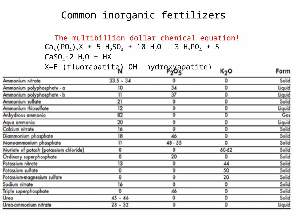
Common inorganic fertilizers
The multibillion dollar chemical equation!Ca5(PO4)3X + 5 H2SO4 + 10 H2O → 3 H3PO4 + 5 CaSO4·2 H2O + HXX=F (fluorapatite) OH hydroxyapatite)
NO2OP
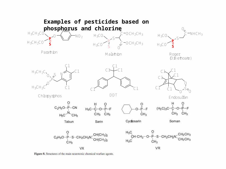
H3CH2CO
SH3CH2CO
Parathion
OCH2CH3C
C OCH2CH3
SP
H3CO
SH3CO
O
O
Malathion
NHCH3CS
P
H3CO
SH3CO
O
Roger (Dimethoate)
ClCl
ClCl
Cl
DDTO
S
O
O
Cl ClCl
Cl
Cl Cl
Endosulfan
N
PSO
O
H3CH2C
H3CH2C
Cl
Cl
Cl
Chlorpyriphos
Examples of pesticides based on phosphorus and chlorine
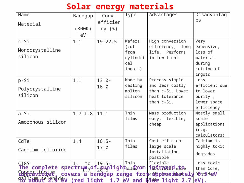
Name
Material
Bandgap (300K) eV
Conv. efficiency
(%)
Type Advantages Disadvantages
c-Si Monocrystalline silicon
1.1 19-22.5 Wafers (cut from cylindrical ingots)
High conversion efficiency, long life. Performs in low light
Very expensive, loss of material during cutting of ingots
p-SiPolycrystalline silicon
1.1 13.0-16.0 Made by casting molten silicon
Process simple and less costly than c-Si. Lower heat tolerance than c-Si.
Less efficient due to lower purity , lower space efficiency
a-SiAmorphous silicon
1.7-1.8 11.1 Thin films Mass production easy, flexible, cheap
Mostly small scale applications (e.g. calculators)
CdTeCadmium telluride
1.4 16.5-17.0 Thin films Cost efficient . large scale installation possible
Cadmium is highly toxicdegrades
CIGSCopper indium gallium selenide
1. to 1.7
19.5-20.8 Thin films Flexible substrate, more efficient than CdTe
Less toxic than CdTe, Degrades
Multi Junction (MJ)Indium gallium phosphide;Indium gallium arsenide; Germanium
1.91.40.7
40.7 Thin films Highest conversion efficiency. Application preferred in space
Most expensive. Degrades fast
Solar energy materials
The complete spectrum of sunlight, from infrared to ultraviolet, covers a bandgap range from approximately 0.5 eV to about 2.9 eV (red light 1.7 eV and blue light 2.7 eV).
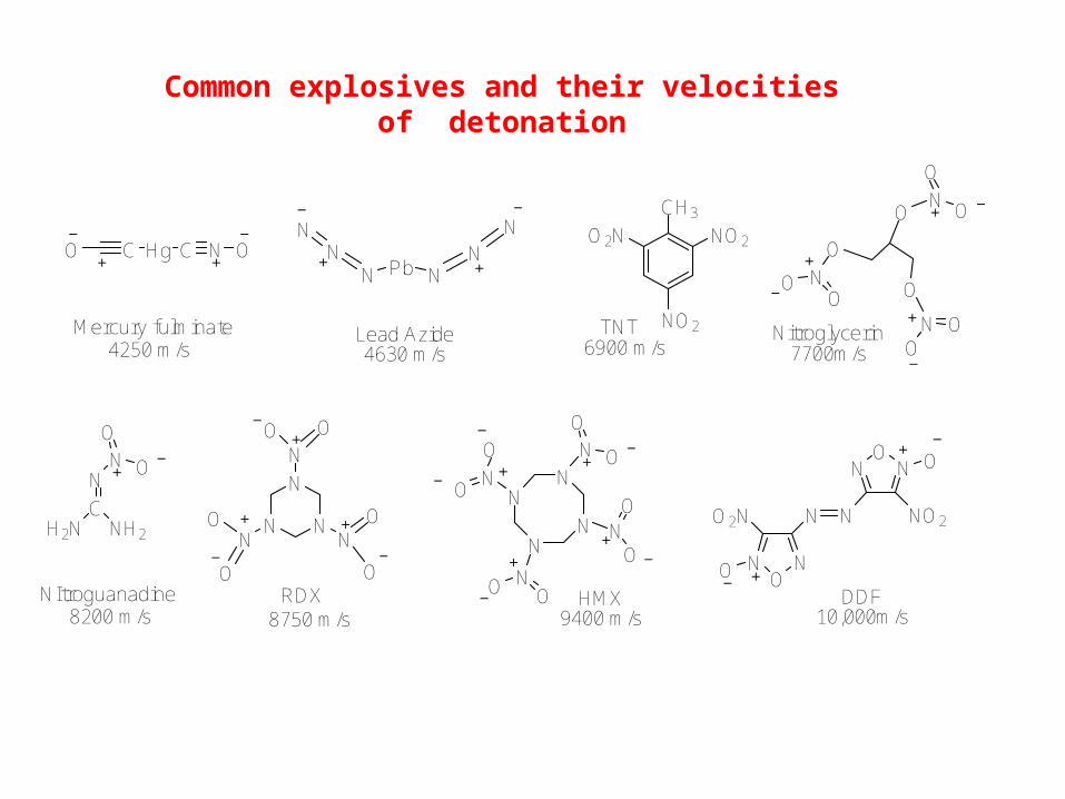
Hg C N OCO
Mercury fulminate
N N
N
N
N
NO
O
O O
O
ORDX
CH2N NH2
NN
O
O
NItroguanadine
4250 m/s
8750 m/s8200 m/s
O
O
ON
O
O
NO
O
N OO
Nitroglycerin7700m/s
HMX9400 m/s
Pb NNN
NN
N
Lead Azide4630 m/s
CH3
NO2
NO2
O2N
TNT6900 m/s
N
NN
NN
O
O
NO
ON
OO
NO
O
ONN
O2N
O
ON N
NO2
O
N N
DDF10,000m/s
Common explosives and their velocitiesof detonation
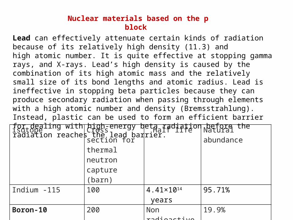
isotope Cross section for thermal neutron capture (barn)
Half life Natural abundance
Indium -115 100 4.41×10¹⁴ years 95.71%Boron-10 200 Non radioactive 19.9%Cadmium- 113 30,000 7.7 x 10¹⁵ years 12.22%Xenon- 135 2,600,000 9.14 hours 0 (Xe-135 is a decay
product of I-135)
Nuclear materials based on the p block
Lead can effectively attenuate certain kinds of radiation because of its relatively high density (11.3) and high atomic number. It is quite effective at stopping gamma rays, and X-rays. Lead’s high density is caused by the combination of its high atomic mass and the relatively small size of its bond lengths and atomic radius. Lead is ineffective in stopping beta particles because they can produce secondary radiation when passing through elements with a high atomic number and density (Bremsstrahlung). Instead, plastic can be used to form an efficient barrier for dealing with high-energy beta radiation before the radiation reaches the lead barrier.
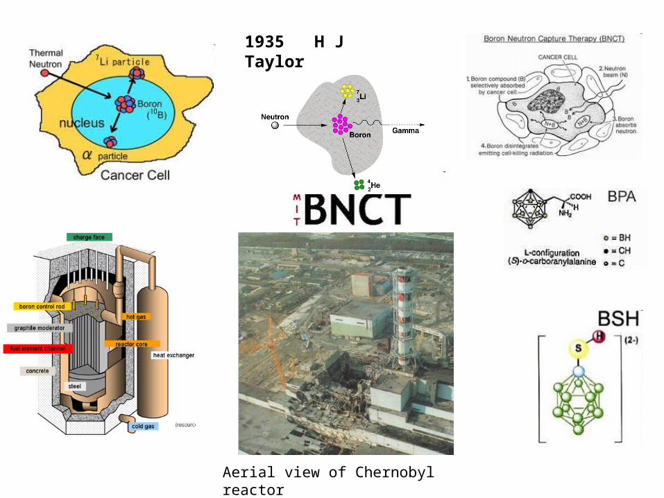
Aerial view of Chernobyl reactor
1935 H J Taylor
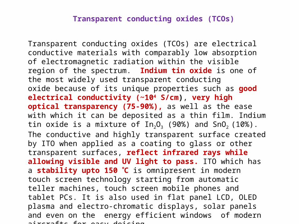
Transparent conducting oxides (TCOs) are electrical conductive materials with comparably low absorption of electromagnetic radiation within the visible region of the spectrum. Indium tin oxide is one of the most widely used transparent conducting oxide because of its unique properties such as good electrical conductivity (~104 S/cm), very high optical transparency (75-90%), as well as the ease with which it can be deposited as a thin film. Indium tin oxide is a mixture of In2O3 (90%) and SnO2 (10%). The conductive and highly transparent surface created by ITO when applied as a coating to glass or other transparent surfaces, reflect infrared rays while allowing visible and UV light to pass. ITO which has a stability upto 150 C is omnipresent in modern touch screen technology starting from automatic teller machines, touch screen mobile phones and tablet PCs. It is also used in flat panel LCD, OLED plasma and electro-chromatic displays, solar panels and even on the energy efficient windows of modern aircrafts for easy deicing.
Transparent conducting oxides (TCOs)
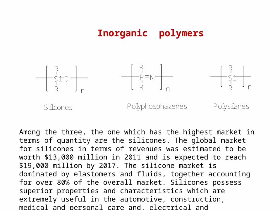
Si O
R
R
Si
R
Rn nP N
R
R n
Silicones Polyphosphazenes Polysilanes
Inorganic polymers
Among the three, the one which has the highest market in terms of quantity are the silicones. The global market for silicones in terms of revenues was estimated to be worth $13,000 million in 2011 and is expected to reach $19,000 million by 2017. The silicone market is dominated by elastomers and fluids, together accounting for over 80% of the overall market. Silicones possess superior properties and characteristics which are extremely useful in the automotive, construction, medical and personal care and, electrical and electronics end-user industries
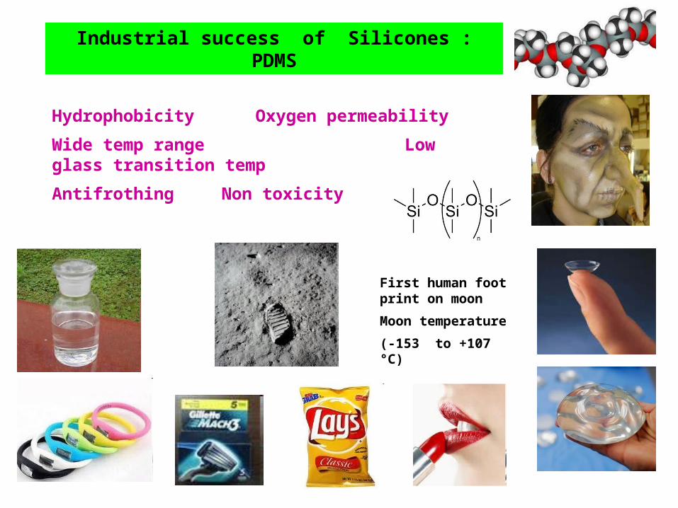
Industrial success of Silicones : PDMS
First human foot print on moon
Moon temperature
(-153 to +107 °C)
Hydrophobicity Oxygen permeability
Wide temp range Low glass transition temp
Antifrothing Non toxicity
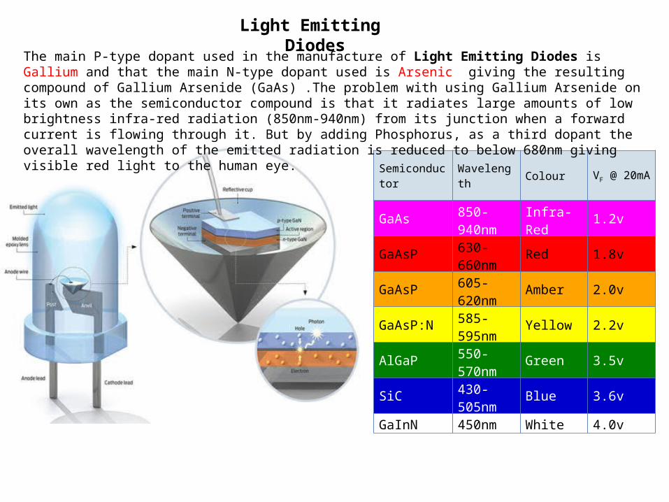
Light Emitting Diodes
Semiconductor Wavelength Colour VF @ 20mA
GaAs 850-940nm Infra-Red 1.2v
GaAsP 630-660nm Red 1.8v
GaAsP 605-620nm Amber 2.0v
GaAsP:N 585-595nm Yellow 2.2v
AlGaP 550-570nm Green 3.5v
SiC 430-505nm Blue 3.6v
GaInN 450nm White 4.0v
The main P-type dopant used in the manufacture of Light Emitting Diodes is Gallium and that the main N-type dopant used is Arsenic giving the resulting compound of Gallium Arsenide (GaAs) .The problem with using Gallium Arsenide on its own as the semiconductor compound is that it radiates large amounts of low brightness infra-red radiation (850nm-940nm) from its junction when a forward current is flowing through it. But by adding Phosphorus, as a third dopant the overall wavelength of the emitted radiation is reduced to below 680nm giving visible red light to the human eye.
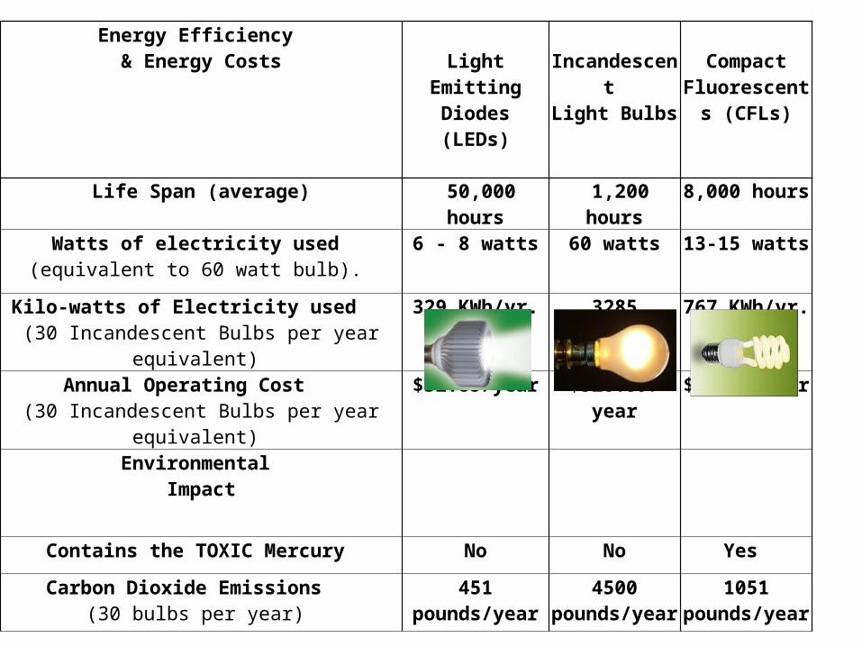
Energy Efficiency & Energy Costs Light Emitting
Diodes (LEDs)Incandescent
Light BulbsCompact
Fluorescents (CFLs)
Life Span (average) 50,000 hours 1,200 hours 8,000 hoursWatts of electricity used
(equivalent to 60 watt bulb). 6 - 8 watts 60 watts 13-15 watts
Kilo-watts of Electricity used (30 Incandescent Bulbs per year equivalent)
329 KWh/yr. 3285 KWh/yr. 767 KWh/yr.
Annual Operating Cost (30 Incandescent Bulbs per year equivalent)
$32.85/year $328.59/year $76.65/year
Environmental Impact
Contains the TOXIC Mercury No No Yes
Carbon Dioxide Emissions (30 bulbs per year)
451 pounds/year 4500 pounds/year
1051 pounds/year
As reagents and catalysts
Lewis acid catalysts based on main group metals such as aluminum, boron, silicon, tin and antimony (BF3, SnCl4, SiF4, SbF5 and AlCl3 ) are used extensively in reactions such as Friedel-Crafts and the aldol reaction, and various pericyclic processes that proceed slowly at room temperature, such as the Diels-Alder reaction, Claisen rearrangement and acetal formation.
The unusual catalytic activity shown by aluminosilicates such as zeolites and clays (e.g. montmorillonite) are unique to the p block elements. The open framework stable structures such as zeolites and ALPO can acts as dehydration and shape selective catalysts. Also of importance are methylating agents such as AlMe3 and its partially hydrolyzed product methyl alumoxane (MAO) which find application as cocatalysts in olefin polymerization reactions
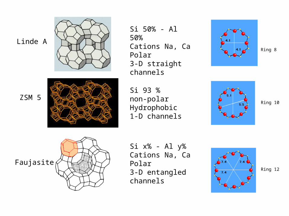
Si x% - Al y%Cations Na, CaPolar3-D entangled channels
FaujasiteRing 12
ZSM 5Si 93 %non-polarHydrophobic1-D channels
Ring 10
Linde A
Si 50% - Al 50%Cations Na, CaPolar3-D straight channels
Ring 8
CH3 OH +(b)
+
(a)
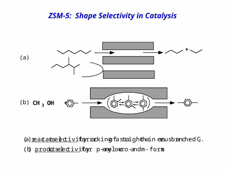
ZSM-5: Shape Selectivity in Catalysis
(a) reactant selectivity for cracking of a straight-chain versus branched C7.
(b) product selectivity for p-xylene over o- and m- forms
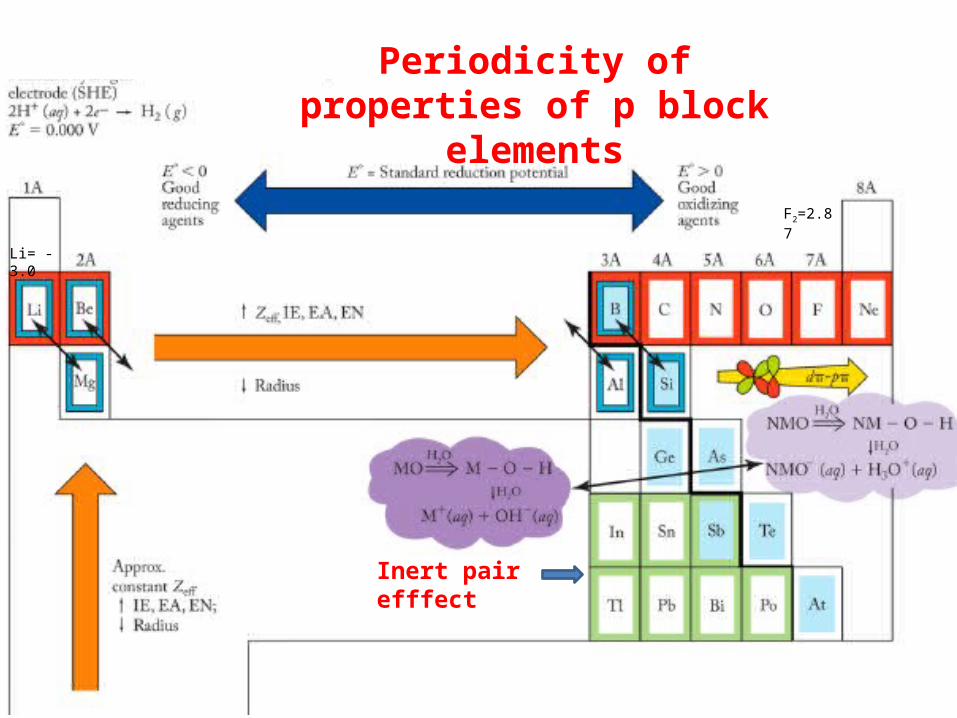
Periodicity of properties of p block elements
Inert pair efffect
F2=2.87
Li= -3.0
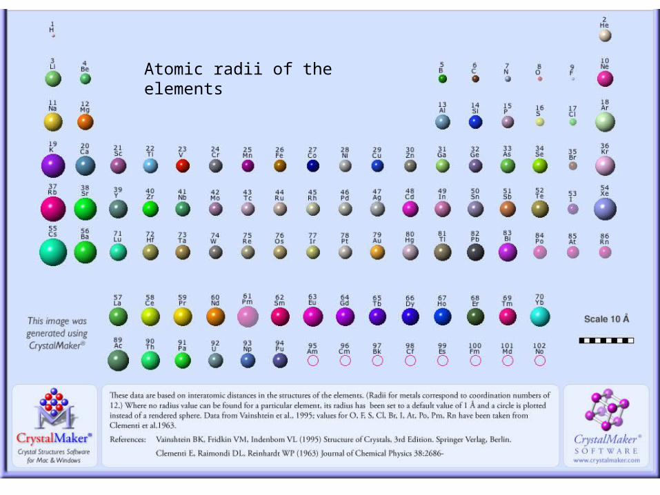
Atomic radii of the elements
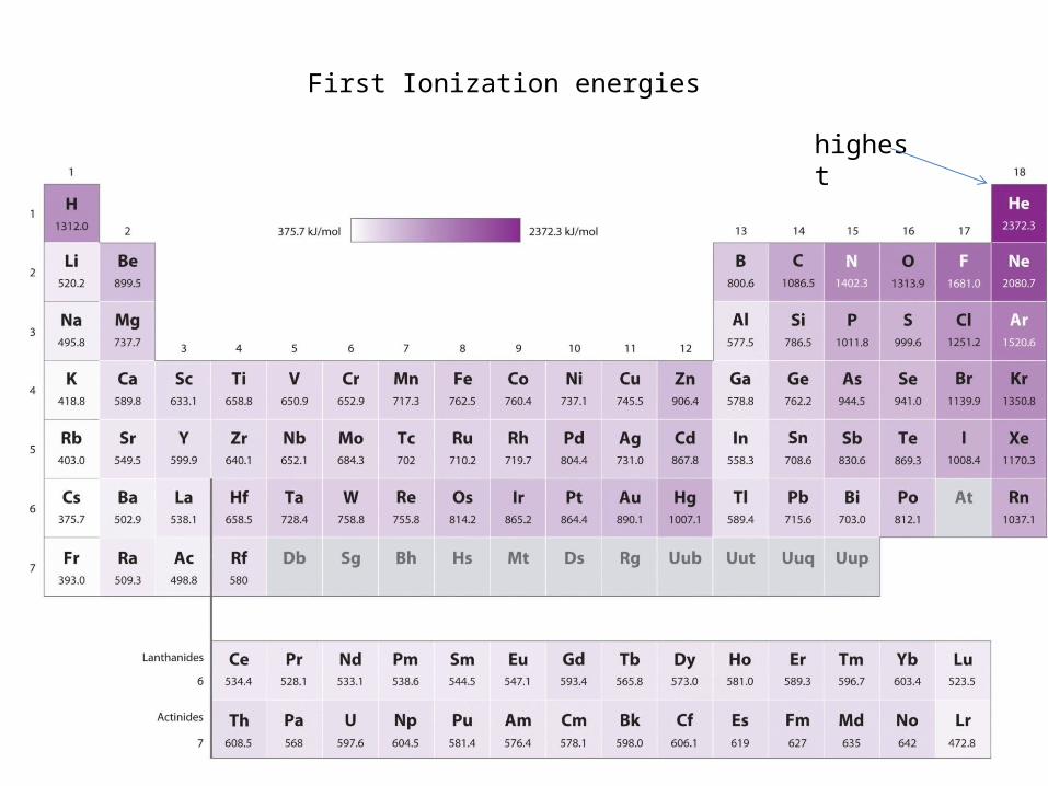
First Ionization energies
highest
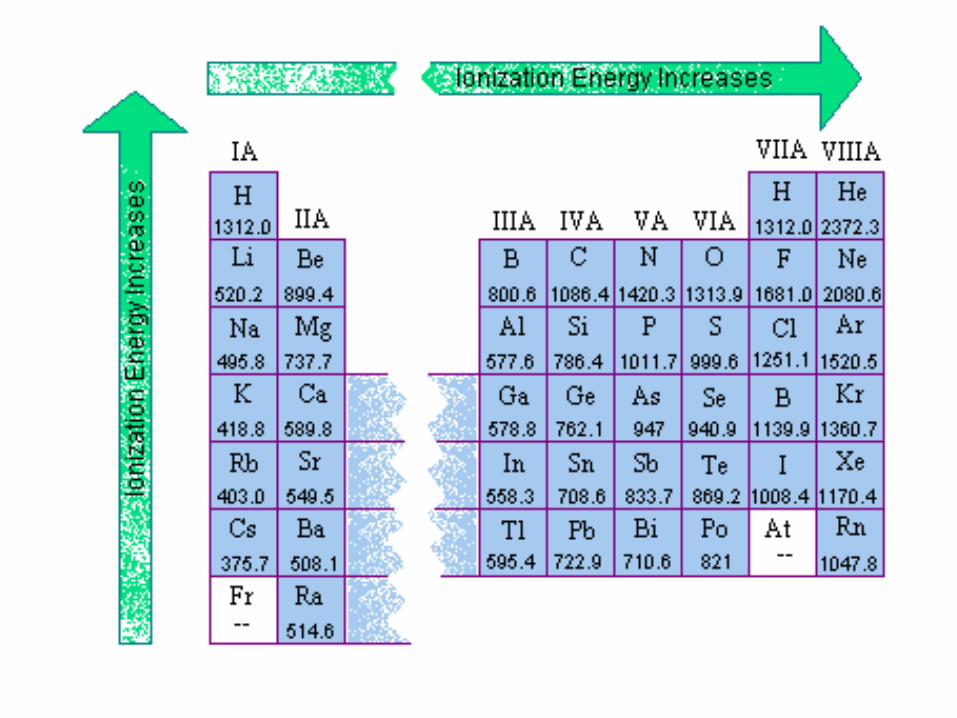
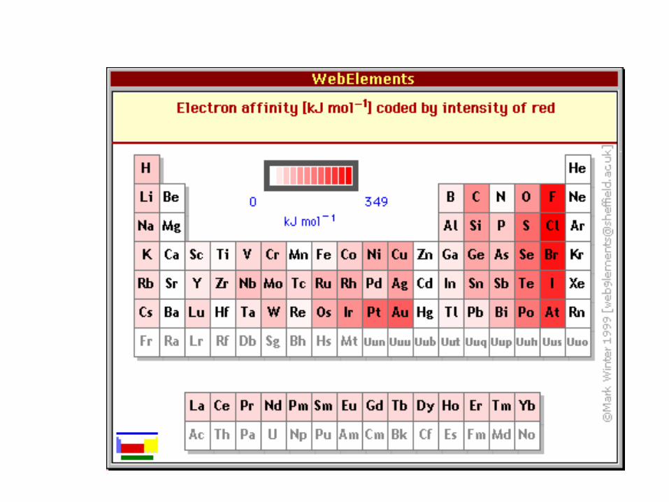
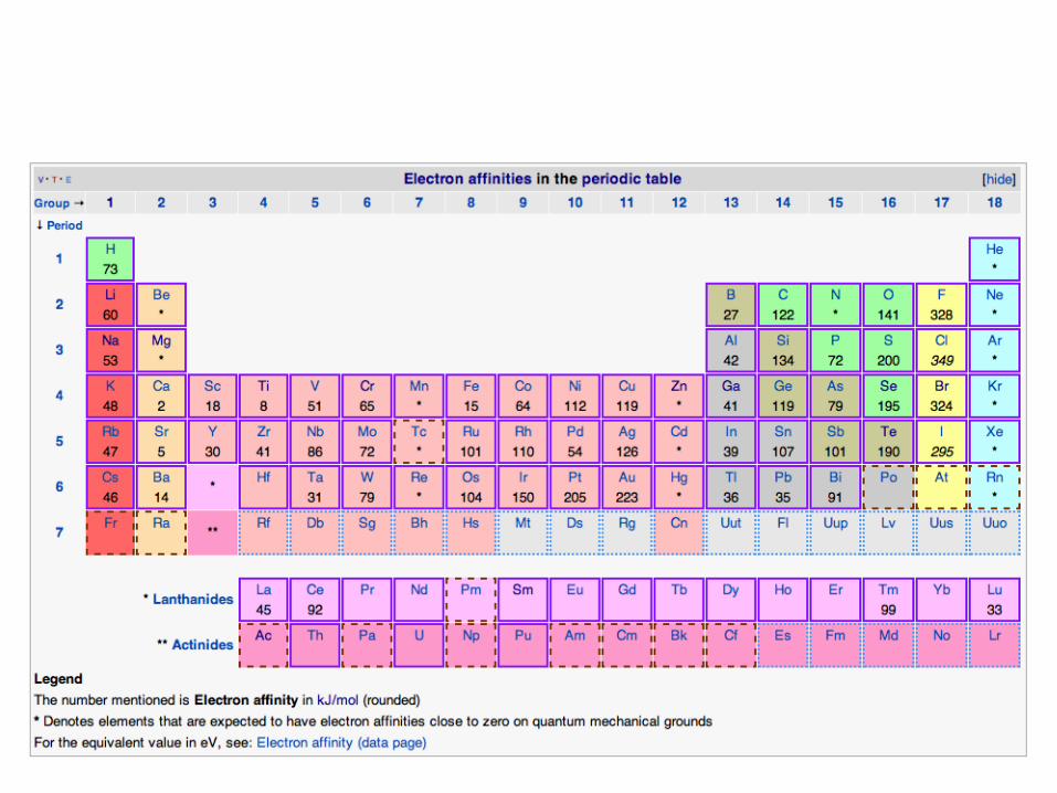
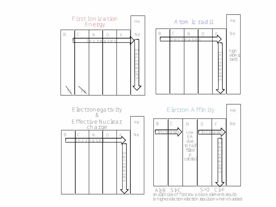
B C N O F Ne
Atom ic radii
D e c r e a s e s
I n c r e
a s e s
B C N O F Ne
First IonizationEnergy
I n c r e a s e s
D e c r e
a s e s
He He
Tl Pb
highatomicradii
B C N O F Ne
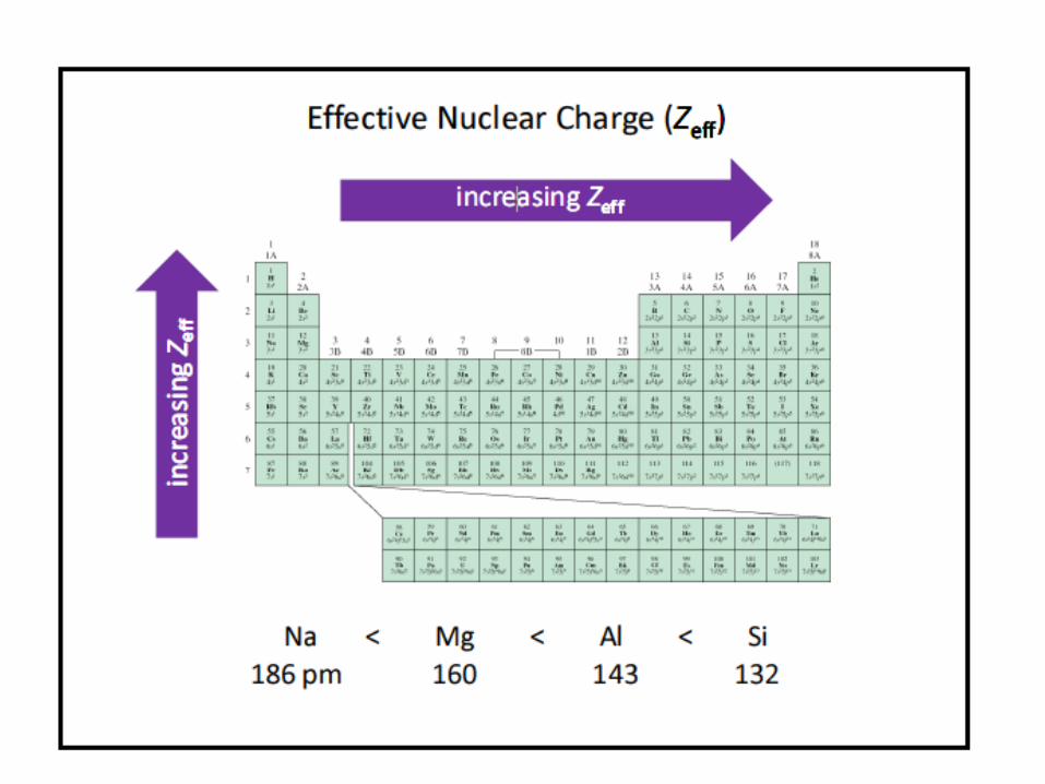
Effective Nuclear charge
I n c r e a s e s
D e
c r e a s e s
He
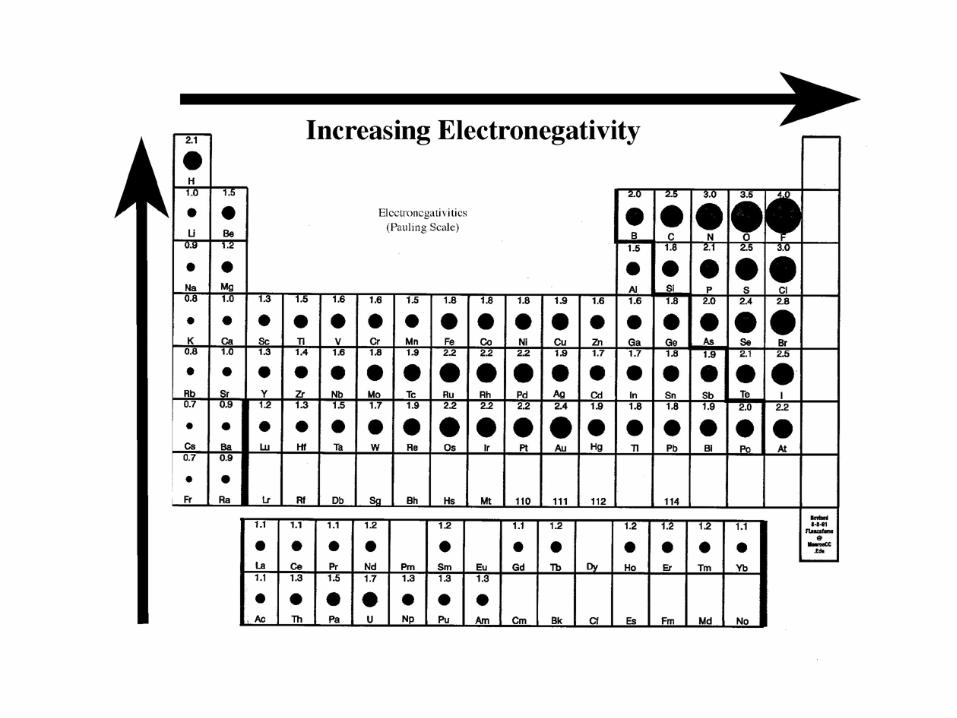
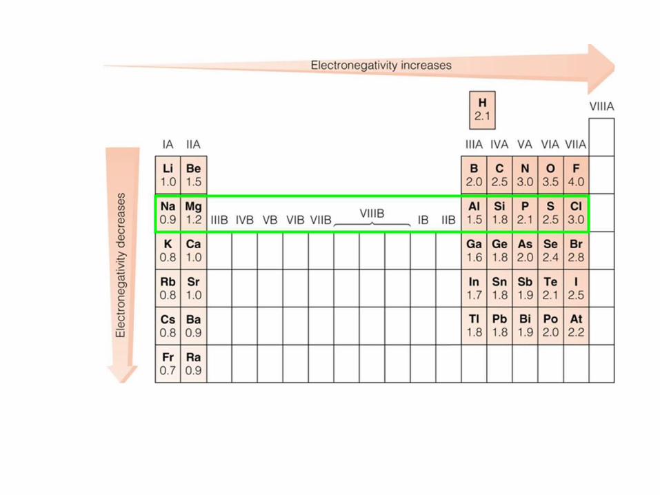
Electronegativity&
B C N O F Ne
Eletron Affinity
Increases
D e c r e
a s e
s
He
IncreasesLowEAdue
to halffilled
porbital
S>O Cl>FSi>CAl>Bsmaller size of f irst row p block elements resultsin higher electron-electron repulsion when e's added
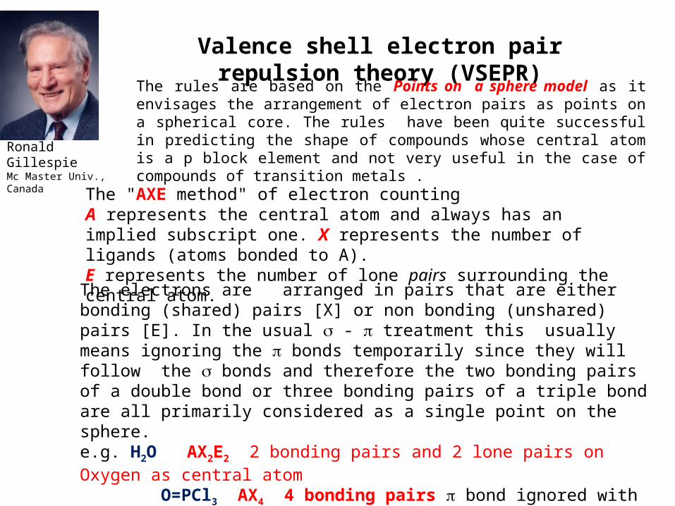
Valence shell electron pair repulsion theory (VSEPR)
Ronald GillespieMc Master Univ., Canada
The rules are based on the Points on a sphere model as it envisages the arrangement of electron pairs as points on a spherical core. The rules have been quite successful in predicting the shape of compounds whose central atom is a p block element and not very useful in the case of compounds of transition metals .
The "AXE method" of electron counting A represents the central atom and always has an implied subscript one. X represents the number of ligands (atoms bonded to A). E represents the number of lone pairs surrounding the central atom.
The electrons are arranged in pairs that are either bonding (shared) pairs [X] or non bonding (unshared) pairs [E]. In the usual - treatment this usually means ignoring the bonds temporarily since they will follow the bonds and therefore the two bonding pairs of a double bond or three bonding pairs of a triple bond are all primarily considered as a single point on the sphere. e.g. H2O AX2E2 2 bonding pairs and 2 lone pairs on Oxygen as central atom O=PCl3 AX4 4 bonding pairs bond ignored with phosphorus as central atom
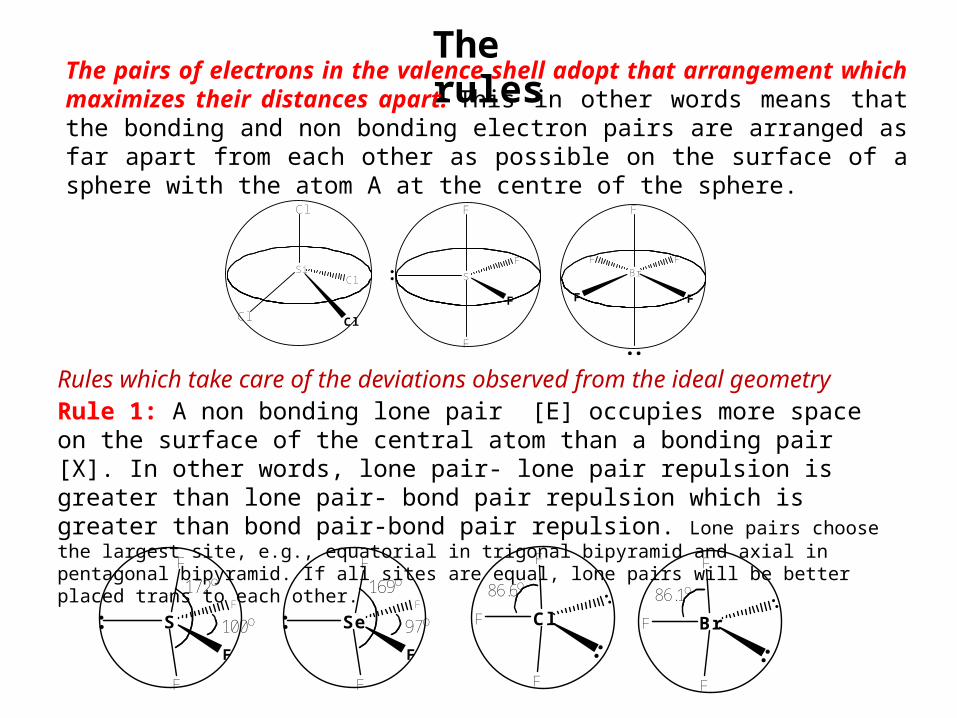
The rulesThe pairs of electrons in the valence shell adopt that arrangement which maximizes their distances apart. This in other words means that the bonding and non bonding electron pairs are arranged as far apart from each other as possible on the surface of a sphere with the atom A at the centre of the sphere.
Rule 1: A non bonding lone pair [E] occupies more space on the surface of the central atom than a bonding pair [X]. In other words, lone pair- lone pair repulsion is greater than lone pair- bond pair repulsion which is greater than bond pair-bond pair repulsion. Lone pairs choose the largest site, e.g., equatorial in trigonal bipyramid and axial in pentagonal bipyramid. If all sites are equal, lone pairs will be better placed trans to each other.
Rules which take care of the deviations observed from the ideal geometry
S
F
F
F
F
172o
100o Se
F
F
F
F
169o
97o F Cl
F
F
86.6o
F Br
F
F
86.1o
S
F
F
F
F
Cl
Si
Cl Cl
ClBr
F
F F
F
F
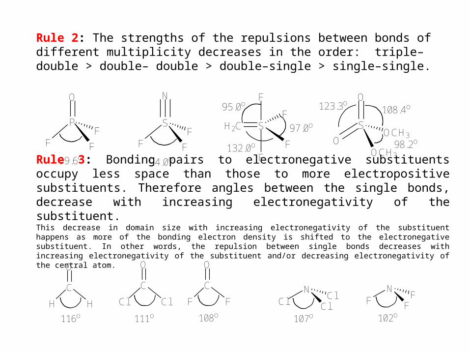
Rule 2: The strengths of the repulsions between bonds of different multiplicity decreases in the order: triple–double > double– double > double–single > single–single.
O
P
F F
F
N
S
F F
F
99.6o 94.0o
H2C S
F
F
F
F
95.0o
97.0o
132.0o
O
S
OOCH3
OCH3
123.3o108.4o
98.2o
Rule 3: Bonding pairs to electronegative substituents occupy less space than those to more electropositive substituents. Therefore angles between the single bonds, decrease with increasing electronegativity of the substituent. This decrease in domain size with increasing electronegativity of the substituent happens as more of the bonding electron density is shifted to the electronegative substituent. In other words, the repulsion between single bonds decreases with increasing electronegativity of the substituent and/or decreasing electronegativity of the central atom.
O
C
H H
116o
O
C
Cl Cl
111o
O
C
F F
108o
NCl Cl
ClN
F FF
107o 102o
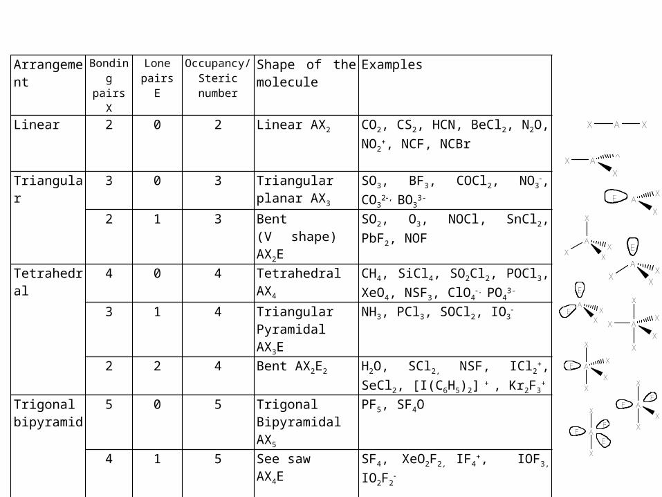
Arrangement Bonding pairs
X
Lone pairs
E
Occupancy/Steric number
Shape of the molecule
Examples
Linear 2 0 2 Linear AX2 CO2, CS2, HCN, BeCl2, N2O, NO2+,
NCF, NCBr
Triangular 3 0 3 Triangular planar AX3
SO3, BF3, COCl2, NO3, CO3
2, BO33-
2 1 3 Bent (V shape) AX2E
SO2, O3, NOCl, SnCl2, PbF2, NOF
Tetrahedral 4 0 4 Tetrahedral AX4 CH4, SiCl4, SO2Cl2, POCl3, XeO4, NSF3, ClO4
. PO43-
3 1 4 TriangularPyramidal AX3E
NH3, PCl3, SOCl2, IO3
2 2 4 Bent AX2E2 H2O, SCl2, NSF, ICl2+, SeCl2,
[I(C6H5)2] + , Kr2F3+
Trigonal bipyramid
5 0 5 TrigonalBipyramidal AX5
PF5, SF4O
4 1 5 See sawAX4E
SF4, XeO2F2, IF4+, IOF3, IO2F2
3 2 5 Bent T shapeAX3E2
ClF3, BrF3, XeOF2, I(Ph)[(CF3C(O)O)]2
2 3 5 LinearAX2E3
XeF2, I3, ICl2
, BrF2. (C6F5)2Xe
AX X
X A
X
X
A
X
XE
X
A
XX
X
A
XX
X
E
A
XX
E
E
X A
X
X
X
X
A
X
X
X
X
E
A
X
X
X
EE
A
X
X
EE
E
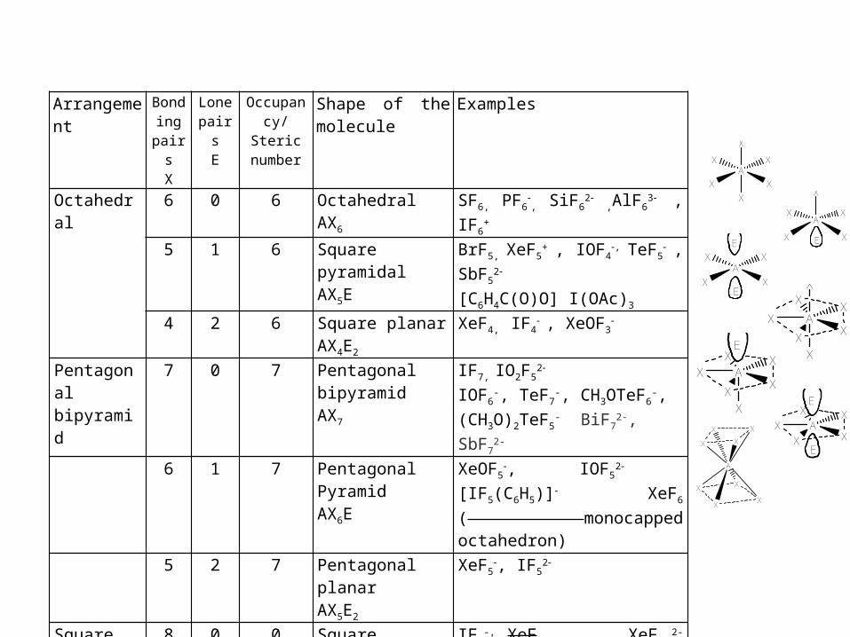
Arrangement Bonding
pairsX
Lone pairs
E
Occupancy/
Steric number
Shape of the molecule
Examples
Octahedral 6 0 6 OctahedralAX6
SF6, PF6, SiF6
2 ,AlF6
3 , IF6+
5 1 6 Square pyramidalAX5E
BrF5, XeF5+ , IOF4
, TeF5 , SbF5
2
[C6H4C(O)O] I(OAc)3
4 2 6 Square planarAX4E2
XeF4, IF4 , XeOF3
Pentagonal bipyramid
7 0 7 Pentagonal bipyramidAX7
IF7, IO2F52
IOF6-, TeF7
-, CH3OTeF6-,
(CH3O)2TeF5- BiF7
2-, SbF72-
6 1 7 PentagonalPyramidAX6E
XeOF5, IOF5
2 [IF5(C6H5)] XeF6 ( monocapped octahedron)
5 2 7 Pentagonal planarAX5E2
XeF5, IF5
2
Square antiprism
8 0 0 Square antiprismAX8
IF8-, XeF8, XeF8
2- (AX8E)
AX
X X
X
X
X
A
X
X X
X
X
E
AX
X X
X
E
E
XX
X
XX
A
X
XXXX
XX
A
X
E
XXX
X XA
E
E
X
X
X
X
X
XX
A
X
Shapes of compounds having odd number of electrons
The odd electron also has an influence on the molecular geometry similar to a normal lone pair but of relatively lesser strength. As a result, the geometry will be midway between the molecule with a full electron pair and the molecule with one less electron pair on the central atom. Nitrogen dioxide (NO2) (AX2E0.5) bent shape with an ONO angle 134.
NO2 which is AX2E is also bent but has an ONO angle approximately of 120
while NO2+ (AX2) is linear .
Similarly ClO2 (AX2E1.5) with a lone pair and an unpaired electron has OClO angle of 117.6 while ClO2
with two lone pairs (AX2E2) has a OClO angle of 111.
Exceptions to the VSEPR rules
1. Metal complexes and organometallic compounds based on transition elements
2. Many triatomic alkaline earth metal dihalides, although expected to be linear have been found to be bent (approximate X-M-X angles: CaF2, 145°; SrF2, 120°; BaF2, 108°; SrCl2, 130°; BaCl2, 115°; BaBr2, 115° and BaI2, 105°). Gillespie has proposed that the reason for the same is due to loss of spherical symmetry of the inner shell of the metal atom due to polarising effect of the relatively electronegative halide substituent’s.Li2O also is linear although it is expected to be bent and this has been ascribed to the bonding being more ionic resulting in repulsion between the lithium atoms.
3. The silyl ether O(SiH3)2 has a relatively larger Si-O-Si angle (144.1°), while similar bond angles of Cl2O (110.9°) and (CH3)2O (111.7°) are in the expected range.
Gillespie's rationalization for this observation is that the localization of the lone pairs, and therefore their ability to repel other electron pairs, is greatest when the ligand has an electronegativity similar to or greater than, that of the central atom. When the central atom is more electronegative, as in O(SiH3)2, the lone pairs are less well-localised and have therefore a weaker repulsive effect.
4. Some molecules in which the central atom is from periods 3 and 4 and in which the ligands are less electronegative, do not have sufficient space in their valence shell to accommodate six bonding domains and a large lone pair domain. In such molecules the lone pair is squeezed into a spherical domain surrounding the core and inside the bonding domains (stereochemically inactive s orbital) which therefore have an octahedral arrangement. Thus some AX6E molecule such as SeCl6
2- and TeBr62- have a regular octahedral shape but with longer than normal
bonds.
Some new developments
The electron pair domain model proposed by Gillespie and Harigittai in 1991 followed by Gillespie and Robinson in 1996. This model was based not on pairs of electrons but on a region in space where there is more probability of finding an electron pair (bonding or lone pair). An electron pair domain is a region in space where there is an enhanced probability of finding an electron pair. An electron pair domain extends around the most probable position of finding an electron pair as determined by the Pauli principle and the probability decreases on increasing the distance from the most probable position.
A lone pair domain can in general be thought of as more spread out and larger than a bonding pair domain as the electrons of a lone pair are subject to the attraction of only one atomic nucleus while those of a bonding air are subject to the attraction of two nuclei taking part in the bond formation. A bonding pair domain therefore taken up less space around a nucleus compared to a lone pair domain because the former is stretched out more towards the ligand/ substituent of the central atom. Why a lone pair occupies more space than a bonding pair is well explained by the domain concept.
N
FFF
Lone pair domain
Bonding pair domain
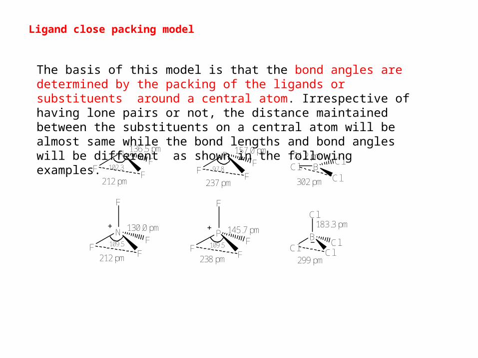
Ligand close packing model
The basis of this model is that the bond angles are determined by the packing of the ligands or substituents around a central atom. Irrespective of having lone pairs or not, the distance maintained between the substituents on a central atom will be almost same while the bond lengths and bond angles will be different as shown in the following examples.
N
FF
F
F
N
FF
F
212 pm
212 pm
136.5 pm
130.0 pm
102.3
109.5
P
FF
F
F
P
FF
F
237 pm
238 pm
157.0 pm
145.7 pm
97.8
109.5
Cl BCl
Cl
Cl
BCl Cl
Cl
174.2 pm
302 pm
299 pm
183.3 pm
Platonic Solids423 BC 347 BC
Archimedian Solids