Embed Size (px)
Citation preview

1
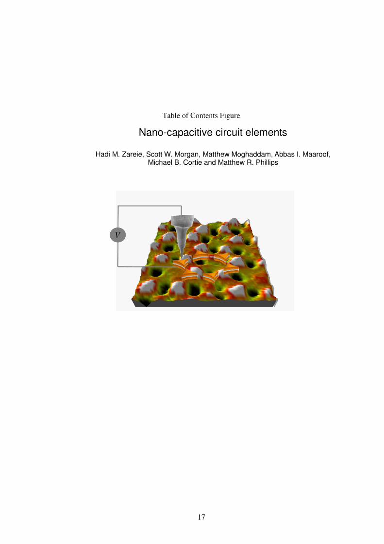
Nano-capacitive circuit elements
Hadi M. Zareie*1, Scott W. Morgan2, Matthew Moghaddam1, Abbas I. Maaroof1,
Michael B. Cortie1 and Matthew R. Phillips2
1Institute for Nanoscale Technology and 2Microstructural Analysis Unit,
University of Technology Sydney, PO Box 123, Broadway NSW 2007, Australia
*e-mail: [email protected],
RECEIVED DATE
*Hadi M. Zareie; Tel: +61-2-9514 8330, Fax: +61-2-9514 8349, E-mail: [email protected]
ABSTRACT. ‘Natural’ lithography was used to prepare arrays of nanoscale capacitors on
silicon. The capacitance was verified by a novel technique based on the interaction of a
charged substrate with the electron beam of a scanning electron microscope. The ‘nano-
capacitors’ possessed a capacitance of ~1 x 10-16 F and were observed to hold charge for
over an hour. Our results indicate that fabricating nanostructures using natural lithography
may provide a viable alternative for future nano-electronic devices.
KEYWORDS: natural lithography, nanocapacitor, scanning probe microscopy, scanning
electron microscopy

2
The progressive miniaturization of electronic devices is a significant challenge. Although the
mainstream approach is to extend conventional optical lithography into the deep ultra-violet
range, there are diverse other schemes under investigation including x-ray lithography, ion
beam lithography, electron beam lithography, and laser interference lithography.
‘Nanosphere lithography’ (NSL) or ‘natural lithography’ offers a surprisingly simple, albeit
rather limited, alternative, which is suitable particularly for periodic arrays of nanometer-scale
structures. This technique appears to been pioneered by Deckman in the 1980s1, 2 (as
‘natural lithography’) and picked up (and renamed to ‘nanosphere lithography’) by Van
Duyne, Hulteen and co-workers, in the mid 1990s3. These schemes have been used to make
nano-caps and semi-shells,4-8 diffraction gratings,9 light emitting surfaces,10 and molecular
biosensors.11-13 However, as far as we can determine, NSL has not previously been used to
prepare working circuit elements. Here we describe how the technique can be used to
fabricate tiny capacitors and diodes.
The principle of NSL is illustrated and explained in Fig. 1. The templating sphere is usually
silica or polystyrene, with a diameter in the 50 to 500 nm range. The diameter of the spheres
must be nearly monodisperse, or else an ordered colloidal crystal template will not form.
Here our interest has been in the structures developed on the silicon substrate lying
underneath the mask, but the process can also be used to develop semi-shells and other
interesting shapes on top of the template spheres.4, 7
In the present work we used NSL to lay down an array of triangular Au-Al2O3-Au
nanocapacitors on the 100 surface of n-doped silicon. Polystyrene latex spheres of 200 nm
diameter were used as the mask. The Au layers were applied at 10 nm thickness with high
vacuum DC magnetron sputtering, and the Al2O3 was deposited at a nominal 5 nm thickness
using a high vacuum RF magnetron sputterer. The techniques used are described in detail in
the Methods section. Verification of charge storage (ie. the capacitance) required the
development of a new technique, which we describe fully here. The array of Au/Al2O3/Au

3
nanocapacitors is depicted in Fig. 2. The nanostructures have in-plane widths of roughly 100
nm, and an out-of-plane height of about 25 nm, as determined by AFM.
ba cba c
Figure 1. Schematic illustration of the process of nanosphere lithography (NSL). (a) A
mono- or bi-layered colloidal crystal of a suitable templating particle is developed on
the substrate by some suitable means, (b) The template is top-coated with one or more
materials of interest, usually by physical vapor deposition. Some of the material
deposited penetrates through the interstices and down onto the substrate. (C) The
template is removed, leaving only the material deposited on the substrate.

4
0.35 µm 60 nm
ba
36 nm60 nm
c d
0.35 µm 60 nm
ba
0.35 µm 60 nm
ba
36 nm60 nm
c d
Figure 2. Nanoscale capacitors produced by nanosphere lithography. (a) Low
magnification image produced using AFM. (b) High magnification image produced
using AFM. (c) Low magnification image obtained using STM. (d) High Magnification
image obtained using STM.
Figs. 3 (panels A to H) show secondary electron (SE) images of an array of Au/Al2O3/Au
nanocapacitors (small grey dots) on the Si substrate, acquired as a function of time (t) at a
primary electron (PE) energy, EPE = 0.3 keV; PE beam current, IPE = 100 pA; working
distance, and WD = 3 mm. It can be seen that as the PE beam scans the magnified area of
the image each nanocapacitor becomes increasingly brighter, indicating that the net surface
potential on the top Au electrode is becoming more negative with time (see Materials and
Methods section). It is obvious from the images that the rate at which each nanocapacitor
charges is much greater that the rate at which they discharge as each nanocapacitor
appears brighter with time and hence electron injection dosage. This experiment was
repeated several times for reproducibility. The effect seen in Fig. 3 clearly demonstrates that

5
each of the nanocapacitors is storing charge and therefore acting as a capacitive device. It
should be noted that the leakage current of each nanocapacitor is very small as they
remained bright for several hours to days after they were charged by the PE beam.
Assuming that the detection system used to generate SE images efficiently discriminates
against backscattered electrons (BSEs), such as the in-lens SE detector used in this work, a
plot of the grayscale intensity (GSI) versus time with the PE beam on (when brightness and
contrast settings of the in-lens SE detector remain constant) can be used to represent the
change in the SE emission coefficient and hence the charging characteristics of a
nanocapacitive device (i.e. the rate of charge storage/leakage or the characteristic time
constant (RC)).
Figure 3. SE images of Au(10 nm)-Al2O3(5 nm)-Au(10 nm) nanocapacitors acquired as
a function of time illustrating dynamic charging. (a) t = 0 s; (b) t = 41 s; (c) t = 75 s; (d)
t = 108 s; (e) t = 143 s; (f) t = 177 s; (g) t = 212 s; (h) t = 246 s. [EPE = 0.3 keV, IPE = 100
pA, WD = 3 mm]
In order to estimate the increase in charge stored in each of the nanocapacitors as a function
of time the average GSI, calculated from the consecutive images shown in Fig. 3, has been
plotted versus time, in Fig. 4. The GSI values were measured using Scion Image (Scion
Image for Windows Beta 4.0.2, Scion Corporation, Frederick, MD) for each particular
6
nanocapacitor and were averaged over the entirety of its ~100 nm diameter surface. It can
be seen that the GSI increases with time as a first order exponential function of decreasing
gradient which levels off after approximately 100-150 seconds. This is in agreement with the
electron irradiation experiments of Cazaux et al.15 who found that the negative surface
potential on floating Ag-coated MgO reached steady state in around 75-150 seconds.
Cazaux16 theoretically confirmed these observations by showing that the secondary electron
yield is directly related to the surface potential when the PE penetration range is much less
than the material thickness. The experimental GSI data (square dots) of Fig. 4 was fitted
using the exponential function (dark line),
RC
t
AeGSItGSI
−
∞ −=)( (1)
where A is a fitting constant, GSI∞ is equal to the steady state value of GSI and RC is the
characteristic charging time constant of the nanocapacitor; R being the bulk resistance of the
Al2O3 layer and C the capacitance of the nanocapacitor. The values of GSI∞ and RC,
obtained by fitting the exponential function above to the experimental data, were determined
to be 75 ± 1 and 61 ± 5 seconds, respectively. The room temperature volume resistivity of
the high purity (99%) Al2O3, used to fabricate the capacitive nanostructures herein, was ~1012
Ωm which gives the resistance of the 5 nm thick and 100 nm diameter Al2O3 core of each
nanocapacitor to be 6.4x10¹⁷ Ω and therefore a capacitance of (9.6 ± 0.8) x 10-17 farads.

7
Figure 4. Graph of average grayscale intensity (GSI) versus time for a Au(10 nm)-
Al2O3(5 nm)-Au(10 nm) nanocapacitor.
The capacitance of a plane parallel capacitor can be described by the well-known equation
C = εoεrA/L (2)
where ε0 is the permittivity of free space, εr is the relative permittivity of the dielectric medium
between the electrodes of the capacitor, A is the cross-sectional area of the dielectric and L
is the electrode gap distance. The bulk resistance of the dielectric layer within a capacitor is
R = ρL/A (3)
where ρ is the bulk resistivity of the dielectric. It can therefore be seen from equations (2) and
(3) that the time constant of a plane parallel plate capacitor is
RC = ρεoεr (4)
The relative permittivity of the high purity Al2O3 used to fabricate the capacitive
nanostructures was εr = 9.0. Substituting this value and the value for ρ shown previously into
equation (4) gives the theoretical time constant of the nanocapacitors to be 79 seconds,
which is in reasonable agreement with the experimental value of 61 ± 5 seconds obtained.
Equation (1) gives the theoretical capacitance of the nanocapacitors to be 12 x 10-17 farads,
which is also in reasonable agreement with the experimental value of (9.6 ± 0.8) x 10-17
farads.

8
Monte Carlo simulations of a scanning electron beam incident on a 10 nm Au layer
(representing the top Au electrode) were performed using CASINO.17 The simulations
showed that the maximum penetration range of the 0.3 kV PE beam was 3 nm below the
surface of the 10 nm upper Au electrode. This demonstrates that the nanocapacitors studied
were behaving capacitatively as the increase in pixel intensity, or SE emission, seen in
Figures 3 and 4 was indeed due to an increase in the surface potential of the top Au
electrode rather than an electrostatic field effect from direct charge buildup within the Al2O3
core.
In conclusion, we have demonstrated how nanosphere lithography can be used to fabricate
ordered arrays of capacitive circuit elements, spaced about 100 nm apart. The capacitance
of the Au-Al2O3-Au nanocapacitors was obtained from transient GSI measurements, and was
determined to be (9.6 ± 0.8) x10-17 farads. This is in good agreement with the theoretical
value of 12 x 10-17 farads. The dynamic charging experiments presented above qualitatively
demonstrate that the nanocapacitive structures fabricated in this work are capable of storing
useable amounts of charge for sufficient periods of time. These results imply that fabricated
nanocircuit elements of these types could be incorporated into nanosized electronic circuits,
potentially bringing benefits in terms of a reduction in power requirements and size.
METHODS
The silicon wafer used presented a surface with 100 orientation and n-type doping.
Samples measuring approximately 1 x 1 cm were cut from the wafer and cleaned by
immersion in ‘piranha solution’ at 65 °C for ~15 min. The substrates were rinsed copiously
with high purity water (18 MΩ resistivity), rinsed with absolute ethanol, and dried with
nitrogen gas. Aqueous suspensions of polystyrene spheres with mean diameters of 200 nm
(Spherotech Inc.) were further diluted in a solution of Triton X-100X-100/methanol (1:400 by
volume).

9
The nanosphere lithography (NSL) masks were created by spin coating the suspension of
polystyrene nanospheres onto the silicon substrates at 3600 rpm using a custom-built spin
coater. The entire substrate was spin coated with the nanospheres for 40 seconds.
The specimens were then placed in a high vacuum vapor deposition system, which was
evacuated for a minimum of four hours to yield a base pressure of ~10-4 Pa (10-6 Torr).
Multilayer structures of Au/Al2O3/Au were deposited using high vacuum DC sputtering for the
Au, and RF magnetron sputtering for the Al2O3. The sputtering targets were 99.999% pure
discs (50mm diameter), placed 150 mm away from the substrate. Sputtering was carried out
in presence of flowing Ar, at a pressure of 0.3 Pa (2 mTorr). The thickness of Au used was
the minimum required to produce electrical continuity. An in situ electrical measurement was
used to monitor the Au film during deposition. The method has been described previously.18
The thickness of the Al2O3 layer was monitored by a quartz crystal mounted in the chamber.
After the coating, the substrate was washed with ethanol, and then the polystyrene
nanospheres were removed by placing each specimen in dichloromethane and sonicating for
a minimum of 2 hours.
AFM measurements
A Digital Instruments Multimode Nanoscope III scanning force microscope was used to
obtain topographic data. Imaging was conducted in tapping mode, with 512 x 512 data
acquisitions at a scan speed of 1.4 Hz at room temperature in air. Oxide-sharpened silicon
nitride tips with integrated cantilevers with a nominal spring constant of 0.38 N/m were used.
The gold nanostructure dimensions were measured by a pair of cursors along a reference
line. The cross-sectional and horizontal distances between each pair of cursors were defined
as the width and length of the different nano structures, respectively. The data were obtained
from at least 15 sections of several conjugated gold nanostructures and the average data are
reported here.
The scanning tunneling microscopy was performed at several locations on the
nanostructures and on the clean Si(100) surface using Multimode Nanoscope III. AFM/STM
10
Images were manipulated with the Scanning Probe Image Processor (SPIP) software.
Contrast-enhanced images were obtained by applying a correlation averaging procedure to
analyze repeat particles units and by a applying low-pass filter.
Estimation of charge and leakage currents
There are several approaches to investigate transient charging or discharging within
insulating materials or devices. One approach is to measure the leakage (current flow to
ground) and displacement currents (time variation of trapped charge induced in an external
circuit) from a sample using conventional electrometers. This approach is often
unsatisfactory with nanostructures, as the leakage current is difficult to measure accurately
due to the small size of the device which causes difficulty in connecting the electronic
apparatus. The substrate (e.g. silicon) is often much larger than each nanocapacitor so that
charging/discharging characteristics measured via the specimen current will be those from
the substrate. Another approach is to use electrostatic mirror and deflection techniques.19
Negative charge is first implanted in an insulating sample using a highly energetic electron
beam. The beam energy is then reduced and the electrostatic repulsion of primary electrons
from the charge implanted regions produces mirroring and distortion effects within SEM
images. This is used to provide quantitative spatial and temporal information of the trapped
charge. This technique is also difficult to perform on nanocapacitors due to their small size
and the consequent inability to insert a measurement apparatus, such as a fine conducting
mesh, between them and the substrate. Therefore, an alternative approach is required to
measure dynamic charging within very small devices such as the present ‘nanocapacitors’.
A simple, but rather crude, approach is to monitor the brightness (greyscale intensity (GSI))
of pixels on a particular nanocapacitor as a function of time. Once a calibrated relationship
between the GSI and time is obtained for a particular nanocapacitor this can then be
implemented into theoretically derived expressions that relate the net trapped charge to
emissive SE and BSE signals. As will be revealed, such a technique enables the relative

11
magnitude of the net charge trapped in a nanocapacitor to be determined as a function of
time and hence the time constant for charging can be evaluated.
In conventional high vacuum SEM an increase in the SE emission coefficient or yield (δ)
(brightening of pixels) following electron irradiation represents negative sample charging20.
The resulting negative surface potential (VS) caused by the net increase in the amount of
negative charge injected into the sample surface by the PE beam increases δ by (i)
effectively reducing the work function for SEs16, 20-23 and (ii) retarding the landing energy of
the primary beam, producing more SEs within the escape depth. Brightening of pixels with
time represents dynamic negative charging. Conversely, darkening of pixels corresponds to
the sample losing negative charge in the charge layer, i.e. positive charging. According to the
‘total yield approach’ and the charge conservation law,24 a dynamic equilibrium (steady state
charging condition) is attained when the total electron emission yield from the sample
reaches unity.16, 23, 25 The total emission yield (σ) being the sum of δ and the backscattered
electron (BSE) yield (η). The condition where σ = δ + η = 1 occurs at one of two critical
emission points E1 and E2 on a plot of σ versus electron energy (E), where E2 > E1 16, 21-24. An
insulating sample charges negatively (σ < 1) when either EPE < E1 or EPE > E2. Conversely,
an insulating sample charges positively (σ > 1) when E1 < EPE < E2 16, 23, 24. Theoretical work
detailing the electric fields, surface potentials and transients associated with charging of
dielectrics and conducting materials can be found in the literature.16, 19-24
When an insulating specimen is coated with a floating metallic conductor, such as the
nanocapacitive devices studied here, the total yield approach fails to correctly describe the
charging mechanisms that actually occur. This phenomenon was experimentally justified by
Cazaux15 who reported a negative surface potential for a floating Ag-coating on MgO sample
at PE beam energies of 2-5 keV even though the total yield approach predicts that a positive
surface potential, and hence positive charging occurs. Figure M1 illustrates this by showing a
plot of the surface potential versus PE beam energy, obtained by Cazaux for a 3 nm floating
Ag layer. Hofmann26 reported similar findings, in which the surface potential on ZrO2-coated
alumina was always found to be negative for PE beam energies of 0.2-10 keV. Furthermore,

12
Jbara et al.27 have demonstrated that the surface potential is always negative for a floating
metallic coating on an insulating material and that the surface potential on a floating metallic-
coated insulator is more negative than for the same uncoated insulator.
Figure M1. Surface potential (VS) versus primary electron (PE) beam energy (EPE) for a
3 nm floating Ag-coating on MgO (adapted from Cazaux et al.15).
When the PE penetration range is much smaller than the thickness of the floating metallic
coating, which is the case for the nanocapacitors studied in this work, the injected charge
from the PE beam will redistribute on the surfaces of the Au nanodot electrode.
Consequently the negative surface potential generated on the electrode will be equivalent to
that of a plane parallel capacitor:
r
s
LV
εε
σ
0
−
= (7)
where σ- is the surface charge density on the surface of the metallic coating, L is the
thickness of the dielectric layer, ε0 is the permittivity of free space and εr is the dielectric
constant of the insulator.15, 23
13
Acknowledgement. This work was supported by the University of Technology Sydney. The
authors thank the Microstructural Analysis Unit at UTS.
FIGURE CAPTIONS
Figure 1. Schematic illustration of the process of nanosphere lithography (NSL). (a) A
mono- or bi-layered colloidal crystal of a suitable templating particle is developed on
the substrate by some suitable means, (b) The template is top-coated with one or more
materials of interest, usually by physical vapor deposition. Some of the material
deposited penetrates through the interstices and down onto the substrate. (C) The
template is removed, leaving only the material deposited on the substrate.
Figure 2. Nanoscale capacitors produced by nanosphere lithography. (a) Low
magnification image produced using AFM. (b) High magnification image produced
using AFM. (c-d) High magnification image obtained using STM.
Figure 3. SE images of Au(10 nm)-Al2O3(5 nm)-Au(10 nm) nanocapacitors acquired as
a function of time illustrating dynamic charging. (a) t = 0 s; (b) t = 41 s; (c) t = 75 s; (d)
t = 108 s; (e) t = 143 s; (f) t = 177 s; (g) t = 212 s; (h) t = 246 s. [EPE = 0.3 keV, IPE = 100
pA, WD = 3 mm].
Figure 4. Graph of average grayscale intensity (GSI) versus time for a Au(10 nm)-
Al2O3(5 nm)-Au(10 nm) nanocapacitor.
Figure M1. Surface potential (VS) versus primary electron (PE) beam energy (EPE) for a
3 nm floating Ag-coating on MgO (adapted from Cazaux et al.15).

14
REFERENCES AND NOTES
1. Deckman, H. W.; Dunsmuir, J. H. Applications of Surface Textures Produced with
Natural Lithography. J. Vac. Sci. Technol. B. 1983, 1, 1109-1112.
2. Deckman, H. W.; Dunsmuir, J. H. Natural Lithography. Appl. Phys. Lett. 1982, 41,
377-379.
3. Hulteen, J. C.; Van Duyne, R. P. Nanosphere Lithography - A Materials General
Fabrication Process for Periodic Particle Array Surfaces. J.Vac. Sci. Technol. A.
1995, 13, 1553-1558.
4. Love, J. C.; Gates, B. D.; Wolfe, D. B.; Paul, K. E.; Whitesides, G. M. Fabrication
and Wetting Properties of Metallic Half-Shells with Submicron Diameters. Nano
Letters. 2002, 2, 891-894.
5. Charnay, C.; Lee, A.; Man, S. Q.; Moran, C. E.; Radloff, C.; Bradley, R. K.; Halas N.
J. Reduced Symmetry Metallodielectric Nanoparticles: Chemical Synthesis and
Plasmonic Properties. J. Phys. Chem. B. 2003, 107, 7327-7333.
6. Liu, J.; Cankurtaran, B.; Wieczorek, L.; Ford, M. J.; Cortie, M. B. Anisotropic Optical
Properties of Semitransparent Coatings of Gold Nanocaps. Advanced Functional
Materials. 2006,16, 1457-1461.
7. Liu, J.; Maaroof, A. I.; Wieczorek, L.; Cortie, M. B. Fabrication of Hollow Metal
"Nanocaps" and their Red-Shifted Optical Absorption Spectra. Advanced Materials.
2005, 17, 1276-1281.
8. Liu, J.; Cankurtaran, B.; McCredie, G.; Ford, M. J.; Wieczorek, L.; Cortie M. B.
Investigation of the Optical Properties of Hollow Aluminium 'Nano-Caps'
Nanotechnology. 2005, 16, 3023-3028.
9. Jiang, P. Surface-Templated Nanostructured Films with Two-Dimensional Ordered
Arrays of Voids. Angew. Chem. Int. Ed. 2004, 43, 5625-5628.
10. Huang, Z.; Zhu, J. Growth and Enhanced Emission of Silicon-Germanium
Hemisphere Shell Arrays. Applied Physics Letters. 2007, 91, 013108.

15
11. Stuart, D. A.; Yonzon, C. R.; Zhang, X. Y.; Lyandres, O.; Shah, N. C.; Glucksberg,
M. R.; Walsh, J. T.; Van Duyne, R. P. Glucose Sensing Using Near-Infrared
Surface-Enhanced Raman Spectroscopy. Anal. Chem. 2005, 77, 4013-4019.
12. Yonzon, C. R.; Stuart, D. A.; Zhang, X. Y.; McFarland, A. D.; Haynes, C. L.; Van
Duyne, R. P. Towards Advanced Chemical and Biological Nanosensors - An
Overview. Talanta. 2005, 67, 438-448.
13. Zhang, X.; Yonzon, C. R.; Young, M. A.; Stuart, D. A.; Van Duyne, R. P. Surface-
Enhanced Raman Spectroscopy Biosensors: Excitation Spectroscopy for
Optimisation of Substrates Fabricated by Nanosphere Lithography. IEE Proc.-
Nanobiotechnol. 2005, 152, 195-206.
14. Tuyen, L. T. T.; Vinh, D. X.; Khoi, P. H.; Gerlach, G. Highly Sensitive NOx Gas
Sensor Based on a Au/n-Si Schottky Diode. Sensors and Actuators B. 2002, 84,
226-230.
15. Cazaux, J.; Kim, K. H.; Jbara, O.; Salace, G. J. Charging Effects of MgO Under
Electron-Bombardment and Nonohmic Behavior of the Induced Specimen Current.
J. Appl. Phys. 1991, 70, 960-965.
16. Cazaux, J. Charging in Scanning Electron Microscopy "from Inside and Outside".
Scanning. 2004, 26, 181-203.
17. Drouin, D.; Couture, A. R.; Gauvin, R.; Hovington, P.; Horny, P.; Demers, H. Monte
Carlo Simulation of Electron Trajectory in Solids (CASINO). Version 2.42.
Sherbrooke, Quebec, Canada Universite de Sherbrooke, 2001.
18. Maaroof, A.I.; Evans, B. L. Onset of Electrical-Conduction in Pt and Ni Films. J.
Appl. Physics. 1994, 76, 1047-1054.
19. Belhaj, M.; Odof, S.; Msellak, K.; Jbara, O. Time-Dependent Measurement of the
Trapped Charge in Electron Irradiated Insulators: Application to Al2O3-Sapphire. J.
Appl. Phys. 2000, 88, 2289-2294.
20. Cazaux, J. Some Considerations on the Electric-Field Induced in Insulators by
Electron-Bombardment. Appl. Phys. 1986, 59, 1418-1430.

16
21. Cazaux, J. Some Considerations on the Secondary Electron Emission, Delta, from
e(-) Irradiated Insulators. J. Appl. Phys. 1999, 85(2), 1137-1147.
22. Cazaux, J. Mechanisms of Charging in Electron Spectroscopy. J. Electr. Spectrosc.
Relat. Phenom. 1999, 105, 155-185.
23. Cazaux, J. Scenario for Time Evolution of Insulator Charging Under Various
Focused Electron Irradiations. J. Appl. Phys. 2004, 95, 731-742.
24. Reimer, L. Scanning Electron Microscopy, 1985 Springer-Verlag, Berlin.
25. Zobacova, J.; Frank, L. Specimen Charging and Detection of Signal from Non-
Conductors in a Cathode Lens-Equipped Scanning Electron Microscope. Scanning
2003, 25, 150-156.
26. Hoffmann, A.; Lenkefi, Z.; Szentirmay, Z. Effect of Roughness on Surface Plasmon
Scattering in Gold Films. J. Physics: Cond. Matter. 1998, 10, 5503-5513.
27. Jbara, O.; Belhaj, M.; Odof, S.; Msellak, K.; Rau, E. I.; Andrianov, M. V. Surface
Potential Measurements of Electron-Irradiated Insulators Using Backscattered and
Secondary Electron Spectra from an Electrostatic Toroidal Spectrometer Adapted
for Scanning Electron Microscope Applications. Rev. Sci. Instrum. 2001, 72, 1788-
1795.
17
Table of Contents Figure
Nano-capacitive circuit elements
Hadi M. Zareie, Scott W. Morgan, Matthew Moghaddam, Abbas I. Maaroof, Michael B. Cortie and Matthew R. Phillips
VVVV