Embed Size (px)
Citation preview
PERSPECTIVES IN NANO TECHNOLOGY EDUCATION IN TERMS OF ENGINEERING POINT OF VIEW
Chang K. KimHanyang University
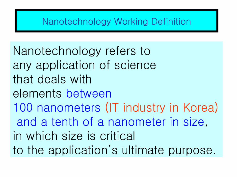
Nanotechnology Working Definition
Nanotechnology refers to any application of sciencethat deals withelements between 100 nanometers (IT industry in Korea)and a tenth of a nanometer in size,in which size is critical to the application’s ultimate purpose.
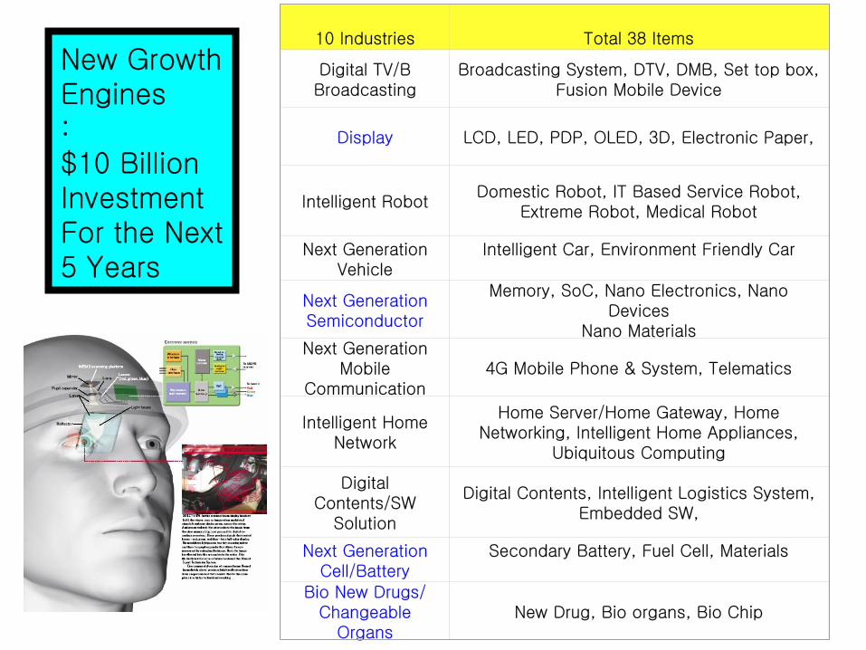
10 Industries Total 38 Items
Digital TV/BBroadcasting
Broadcasting System, DTV, DMB, Set top box, Fusion Mobile Device
Display LCD, LED, PDP, OLED, 3D, Electronic Paper,
Intelligent RobotDomestic Robot, IT Based Service Robot,
Extreme Robot, Medical Robot
Next GenerationVehicle
Intelligent Car, Environment Friendly Car
Next GenerationSemiconductor
Memory, SoC, Nano Electronics, NanoDevices
Nano MaterialsNext Generation
Mobile Communication
4G Mobile Phone & System, Telematics
Intelligent Home Network
Home Server/Home Gateway, Home Networking, Intelligent Home Appliances,
Ubiquitous Computing
Digital Contents/SW
Solution
Digital Contents, Intelligent Logistics System, Embedded SW,
Next GenerationCell/Battery
Secondary Battery, Fuel Cell, Materials
Bio New Drugs/Changeable
OrgansNew Drug, Bio organs, Bio Chip
New GrowthEngines: $10 BillionInvestmentFor the Next5 Years
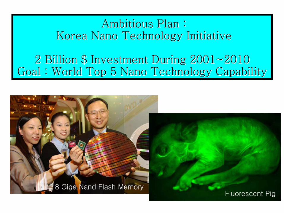
Ambitious Plan :Ambitious Plan :Korea Korea NanoNano Technology InitiativeTechnology Initiative
2 Billion $ Investment During 2001~20102 Billion $ Investment During 2001~2010Goal : World Top 5 Goal : World Top 5 NanoNano Technology CapabilityTechnology Capability
Fluorescent Pig8 Giga Nand Flash Memory8 Giga Nand Flash Memory
Fluorescent Pig
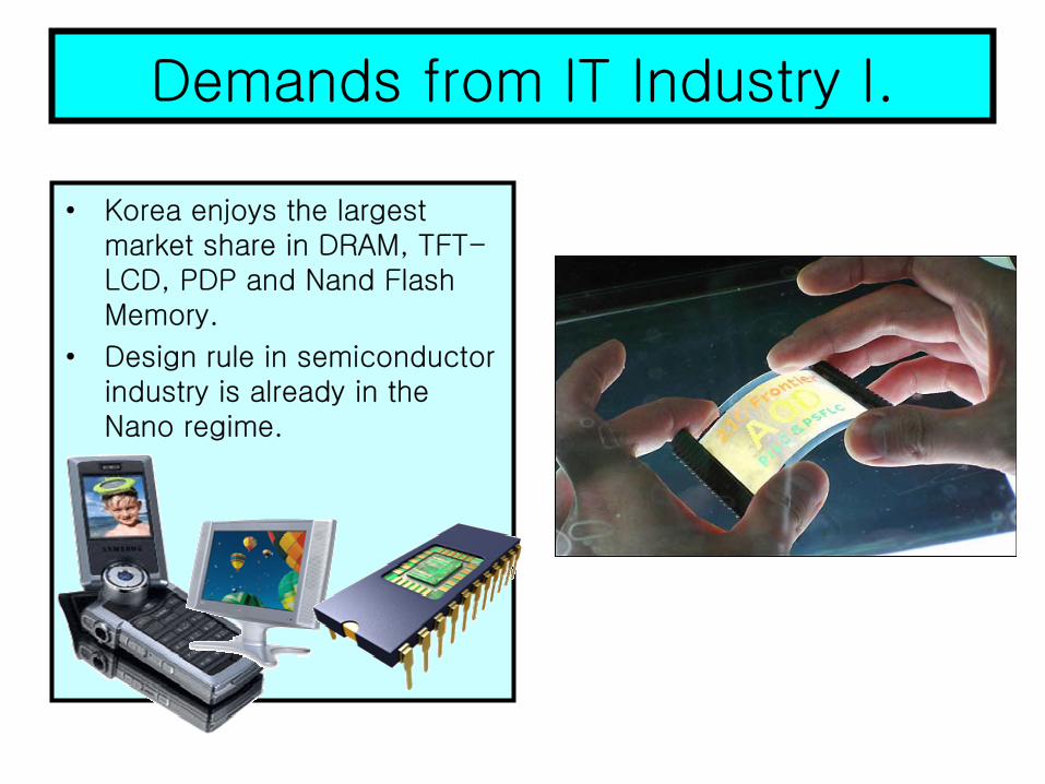
Demands from IT Industry I.
• Korea enjoys the largest market share in DRAM, TFT-LCD, PDP and Nand Flash Memory.
• Design rule in semiconductor industry is already in the Nano regime.
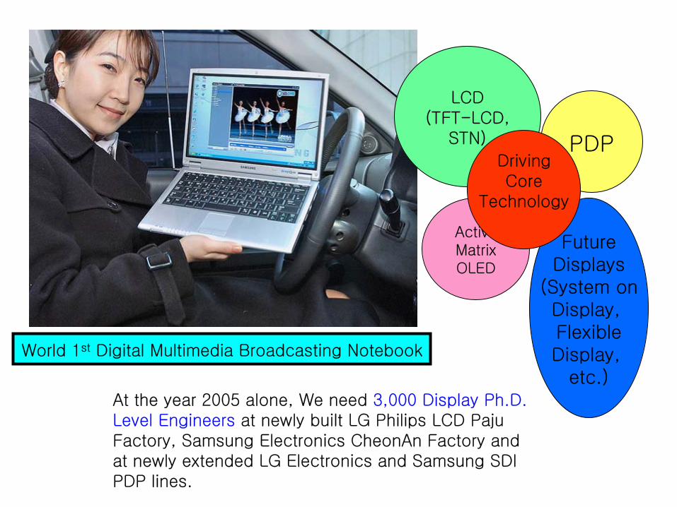
World 1st Digital Multimedia Broadcasting Notebook
At the year 2005 alone, We need 3,000 Display Ph.D. Level Engineers at newly built LG Philips LCD PajuFactory, Samsung Electronics CheonAn Factory and at newly extended LG Electronics and Samsung SDI PDP lines.
LCD(TFT-LCD,
STN) PDP
ActiveMatrixOLED
FutureDisplays
(System onDisplay, FlexibleDisplay,
etc.)
DrivingCore
Technology
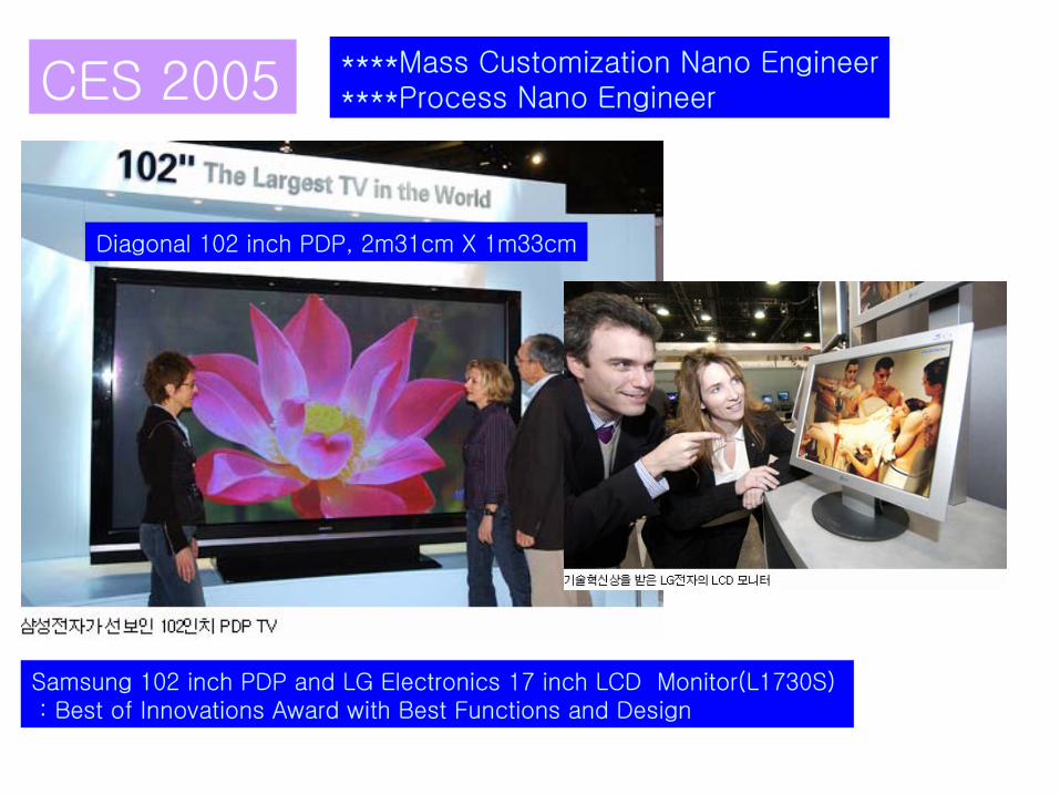
Diagonal 102 inch PDP, 2m31cm X 1m33cm
Samsung 102 inch PDP and LG Electronics 17 inch LCD Monitor(L1730S) : Best of Innovations Award with Best Functions and Design
CES 2005****Mass Customization Nano Engineer****Process Nano Engineer
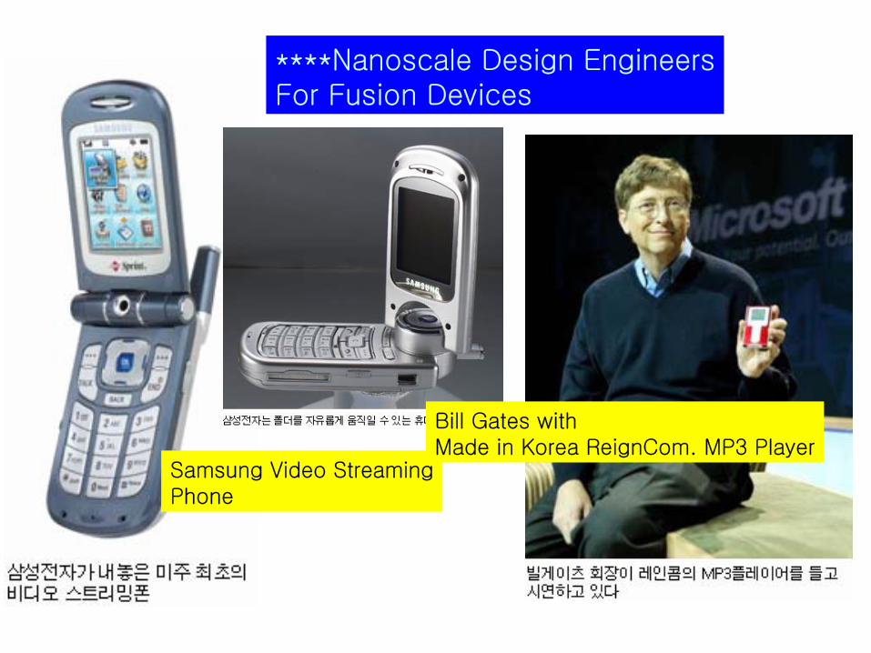
****Nanoscale Design EngineersFor Fusion Devices
Samsung Video StreamingPhone
Bill Gates with Made in Korea ReignCom. MP3 Player
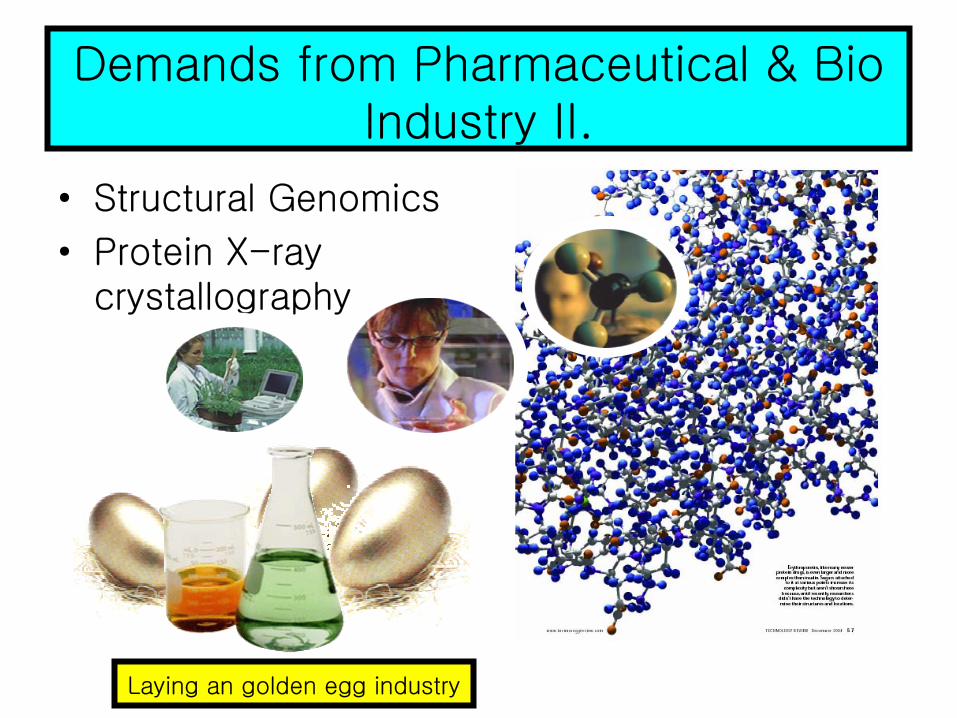
Demands from Pharmaceutical & Bio Industry II.
• Structural Genomics
• Protein X-ray crystallography
Laying an golden egg industry
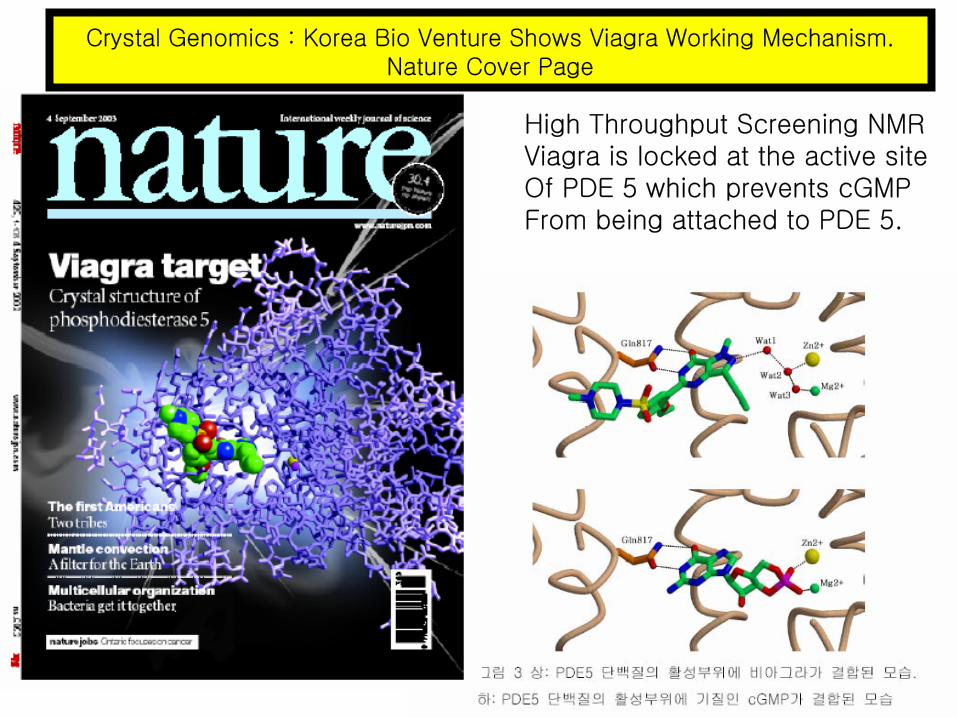
High Throughput Screening NMRViagra is locked at the active siteOf PDE 5 which prevents cGMPFrom being attached to PDE 5.
Crystal Genomics : Korea Bio Venture Shows Viagra Working Mechanism.Nature Cover Page
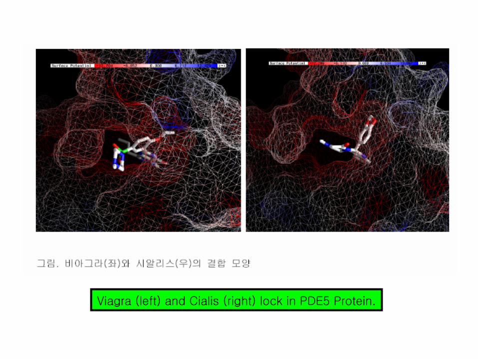
Viagra (left) and Cialis (right) lock in PDE5 Protein.
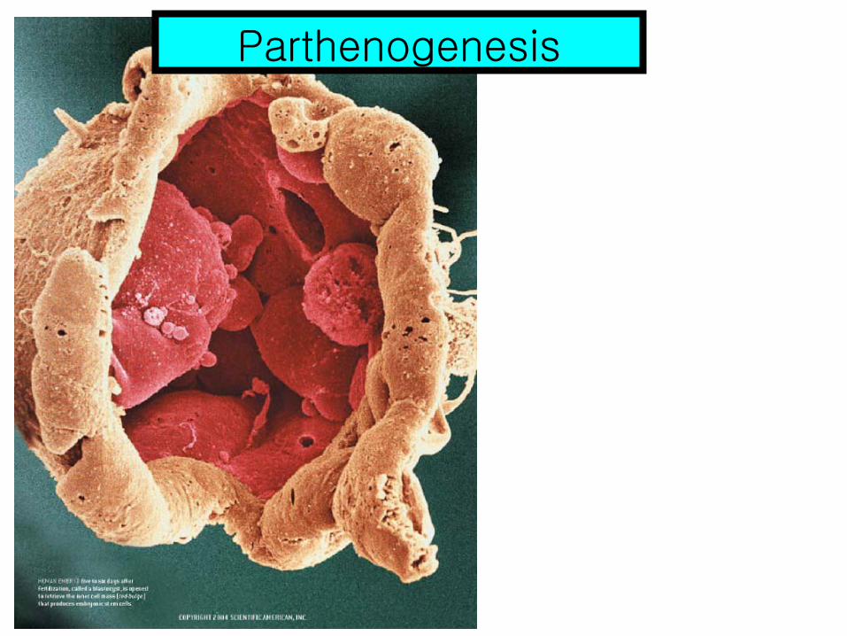
Parthenogenesis

• Researchers in South Korea succeeded in extracting stem cells from a cloned human embryo -- a breakthrough that brings researchers closer to developing individualized disease treatments.
Cloned Embryo Stem Cell
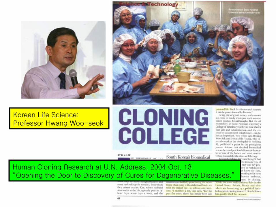
Human Cloning Research at U.N. Address, 2004 Oct. 13“Opening the Door to Discovery of Cures for Degenerative Diseases.”
Korean Life Science: Professor Hwang Woo-seok
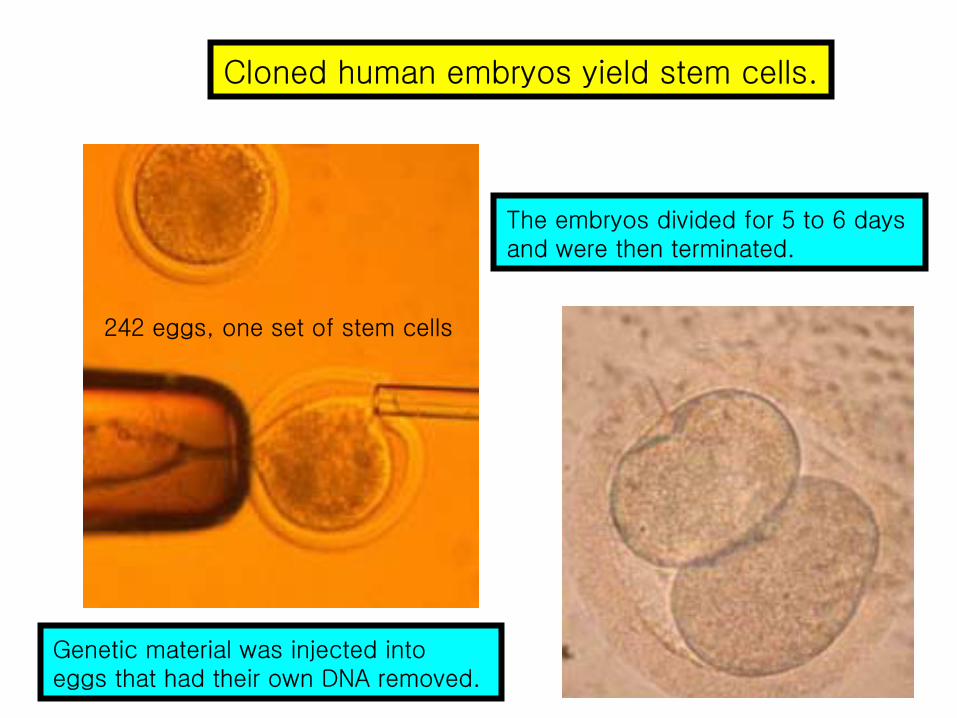
Genetic material was injected into eggs that had their own DNA removed.
242 eggs, one set of stem cells
The embryos divided for 5 to 6 days and were then terminated.
Cloned human embryos yield stem cells.
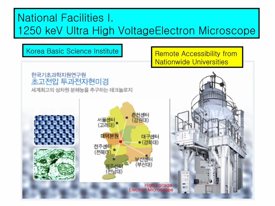
National Facilities I.1250 keV Ultra High VoltageElectron Microscope
Korea Basic Science Institute Remote Accessibility from Nationwide Universities
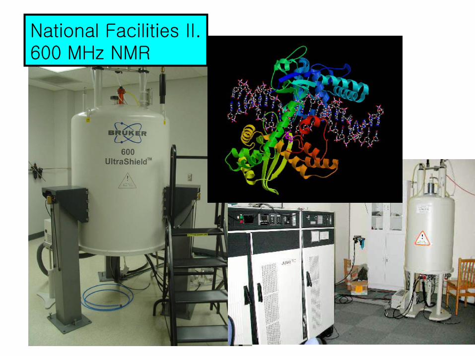
National Facilities II.600 MHz NMR
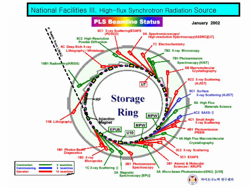
National Facilities III. High-flux Synchrotron Radiation Source
Proteomics,Nano ScaleStructure Determination
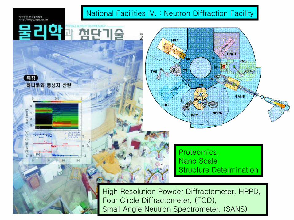
National Facilities IV. : Neutron Diffraction Facility
High Resolution Powder Diffractometer, HRPD, Four Circle Diffractometer, (FCD), Small Angle Neutron Spectrometer, (SANS)
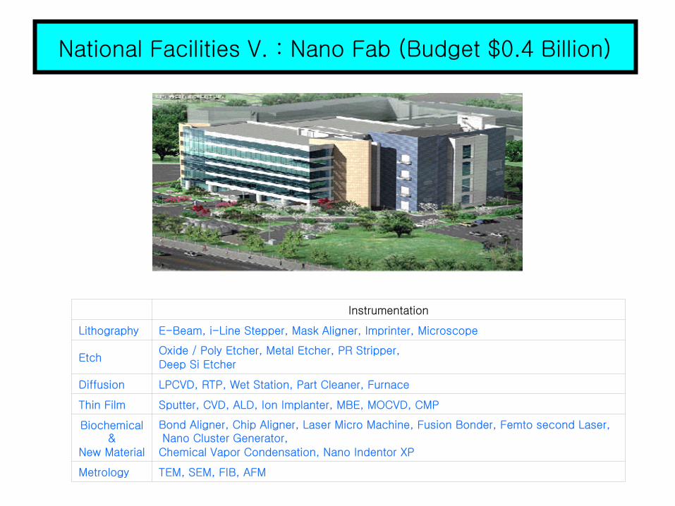
National Facilities V. : Nano Fab (Budget $0.4 Billion)
TEM, SEM, FIB, AFMMetrology
Bond Aligner, Chip Aligner, Laser Micro Machine, Fusion Bonder, Femto second Laser,Nano Cluster Generator, Chemical Vapor Condensation, Nano Indentor XP
Biochemical &
New Material
Sputter, CVD, ALD, Ion Implanter, MBE, MOCVD, CMPThin Film
LPCVD, RTP, Wet Station, Part Cleaner, FurnaceDiffusion
Oxide / Poly Etcher, Metal Etcher, PR Stripper,Deep Si Etcher
Etch
E-Beam, i-Line Stepper, Mask Aligner, Imprinter, Microscope Lithography
Instrumentation
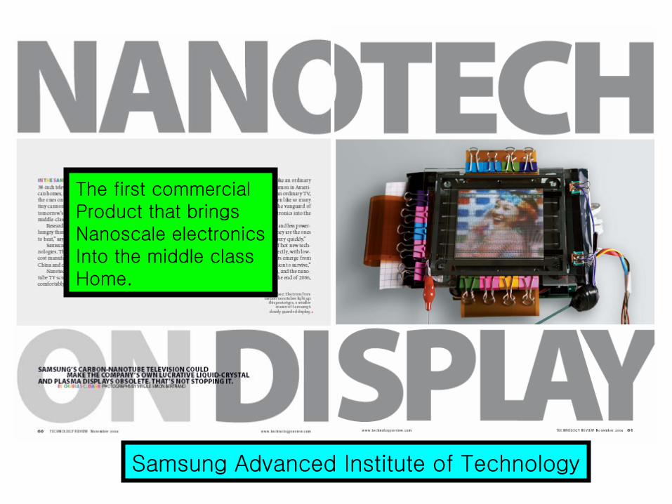
The first commercialProduct that bringsNanoscale electronicsInto the middle classHome.
Samsung Advanced Institute of Technology
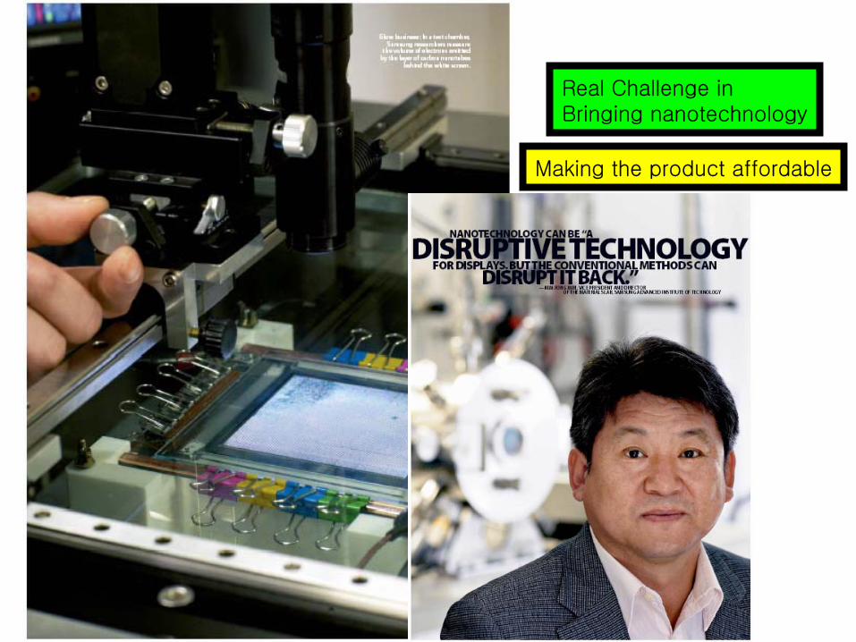
Real Challenge inBringing nanotechnology
Making the product affordable
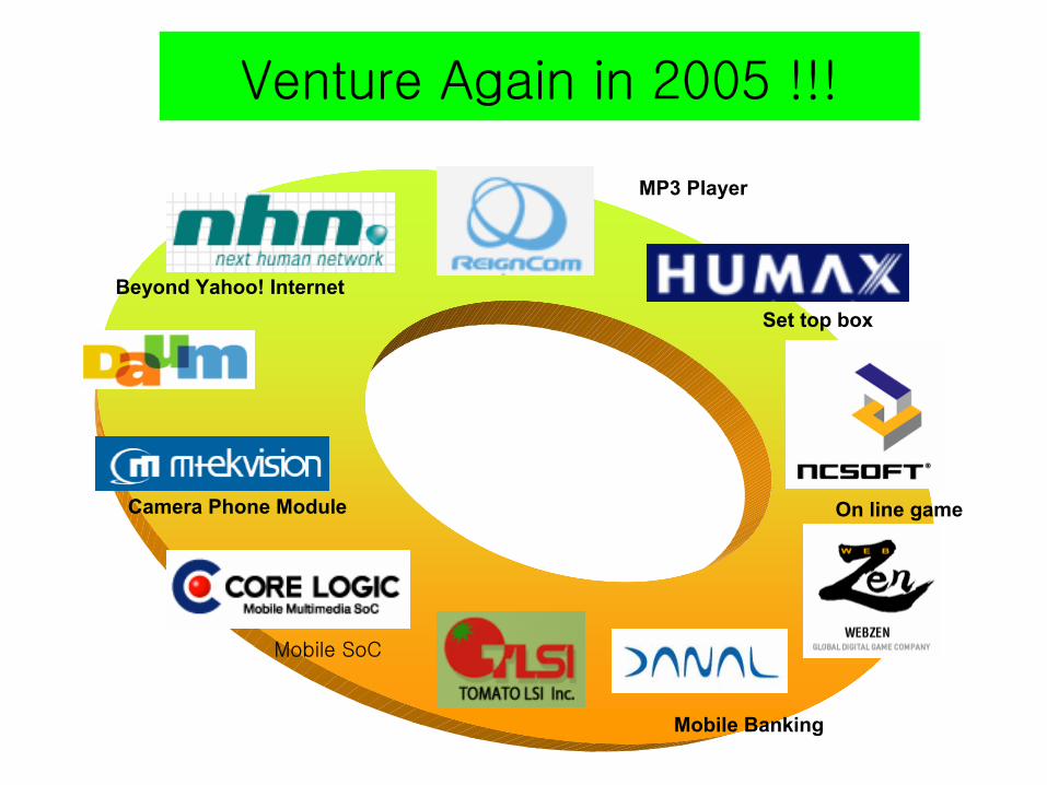
Venture Again in 2005 !!!
Beyond Yahoo! Internet
Camera Phone Module
Mobile Banking
On line game
Set top box
MP3 Player
Mobile SoC
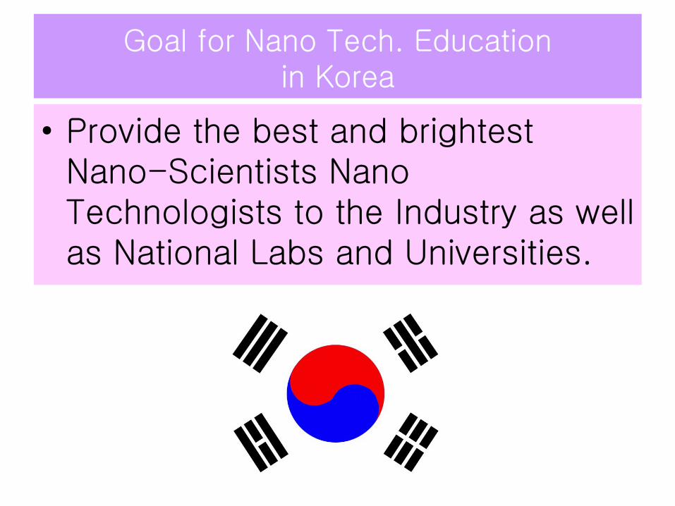
Goal for Nano Tech. Educationin Korea
• Provide the best and brightest Nano-Scientists NanoTechnologists to the Industry as well as National Labs and Universities.
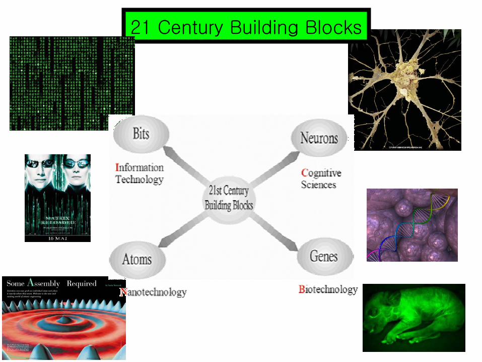
21 Century Building Blocks
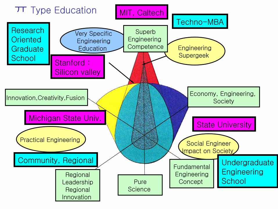
Very SpecificEngineeringEducation Engineering
Supergeek
Innovation,Creativity,Fusion
Practical Engineering Social Engineer
Impact on Society
RegionalLeadershipRegional
Innovation
Economy, Engineering, Society
FundamentalEngineeringConcept
SuperbEngineering Competence
PureScience
ㅠ Type Education MIT, Caltech
Stanford : Silicon valley
Michigan State Univ.State University
Research Oriented GraduateSchool
Community, Regional UndergraduateEngineeringSchool
Techno-MBA
일반 교양
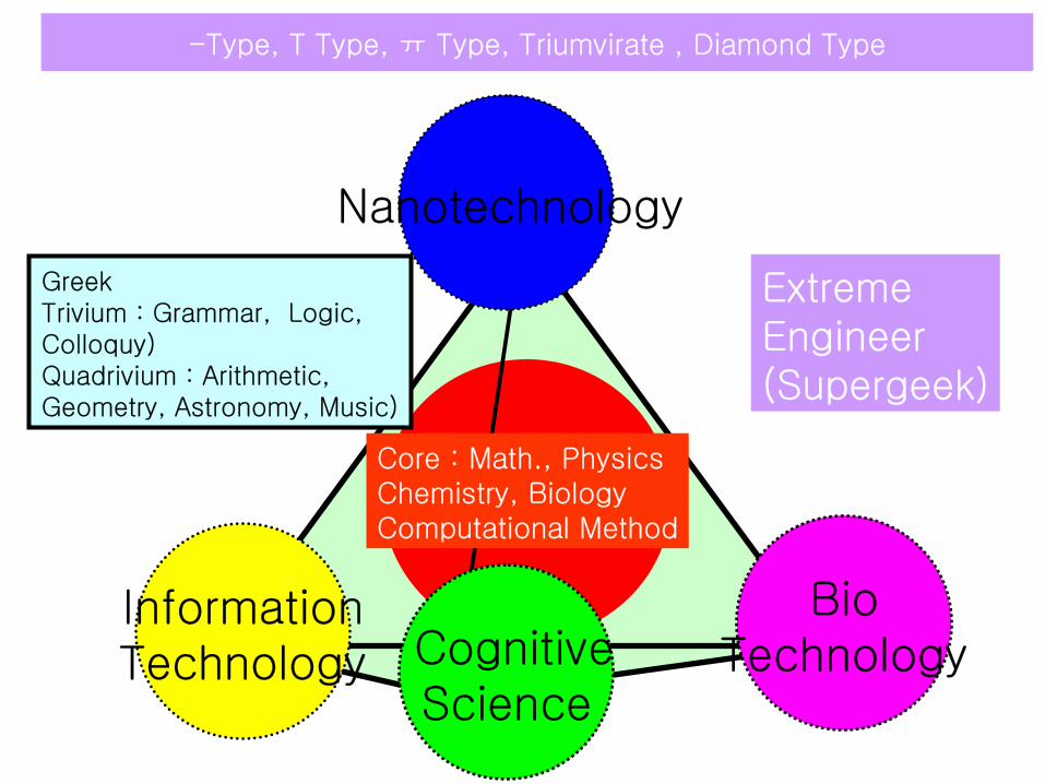
InformationTechnology
Nanotechnology
BioTechnologyCognitive
Science
-Type, T Type, ㅠ Type, Triumvirate , Diamond Type
Core : Math., PhysicsChemistry, BiologyComputational Method
Extreme Engineer(Supergeek)
GreekTrivium : Grammar, Logic, Colloquy)Quadrivium : Arithmetic, Geometry, Astronomy, Music)

Find
Jobs
GraduateSchool
80%
Graudation(100%)
Researcher/Faculty
EngineeringProfessionalsMaster of Engineers
Engineer74%
Master /Ph.D.15%
Career Path after Engineering Schools
Economy, Law : 6Free Choices : 12~18
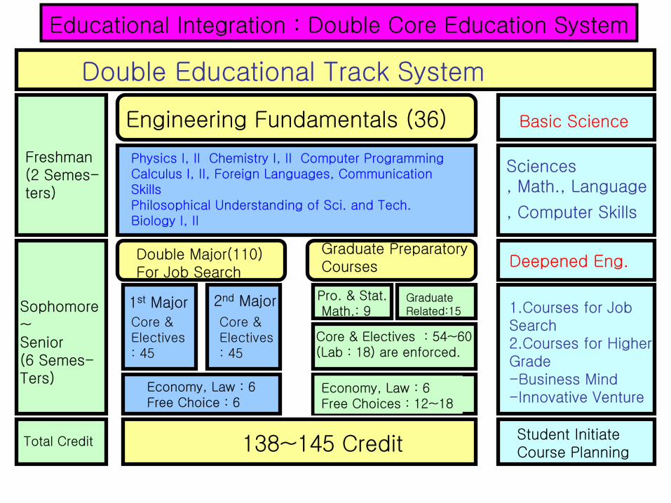
Double Educational Track System
Total Credit
Engineering Fundamentals (36)
Physics I, II Chemistry I, II Computer ProgrammingCalculus I, II, Foreign Languages, Communication SkillsPhilosophical Understanding of Sci. and Tech.Biology I, II
Double Major(110)For Job Search
Graduate Preparatory Courses
1st Major 2nd Major
Core & Electives : 54~60 (Lab : 18) are enforced.
Core &Electives: 45
Core &Electives: 45
Economy, Law : 6Free Choice : 6
138~145 Credit
Freshman(2 Semes-ters)
Sophomore~Senior(6 Semes-Ters)
Basic Science
Sciences, Math., Language
, Computer Skills
Deepened Eng.
1.Courses for Job Search2.Courses for HigherGrade-Business Mind-Innovative Venture
Student InitiateCourse Planning
Pro. & Stat.Math.: 9
GraduateRelated:15
Educational Integration : Double Core Education System
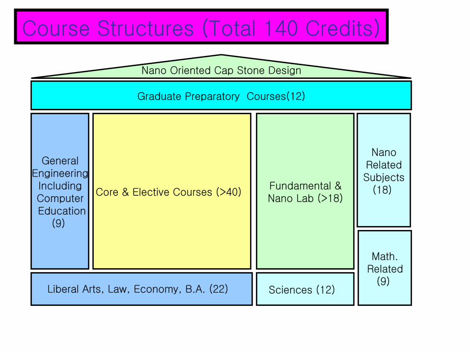
NanoRelatedSubjects
(18)
GeneralEngineeringIncludingComputerEducation
(9)
Fundamental &Nano Lab (>18)
Core & Elective Courses (>40)
Sciences (12)
Graduate Preparatory Courses(12)
Liberal Arts, Law, Economy, B.A. (22)
Math.Related
(9)
Course Structures (Total 140 Credits)
Nano Oriented Cap Stone Design
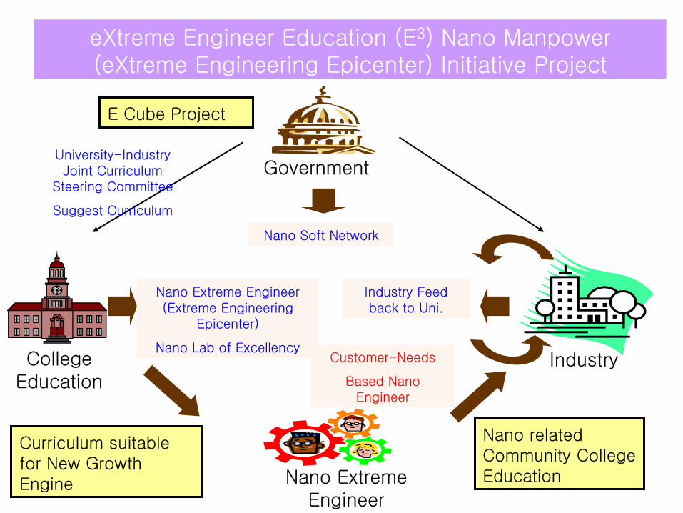
eXtreme Engineer Education (E3) Nano Manpower (eXtreme Engineering Epicenter) Initiative Project
Government
Nano Extreme Engineer
IndustryCollege Education
University-Industry Joint Curriculum
Steering Committee
Suggest Curriculum
Nano Extreme Engineer (Extreme Engineering
Epicenter)
Nano Lab of Excellency
Industry Feed back to Uni.
Customer-Needs
Based NanoEngineer
Nano Soft Network
Curriculum suitable for New Growth Engine
Nano related Community CollegeEducation
E Cube Project
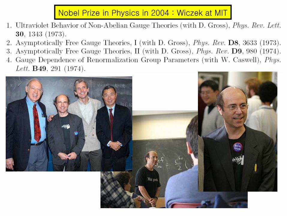
Nobel Prize in Physics in 2004 : Wiczek at MIT
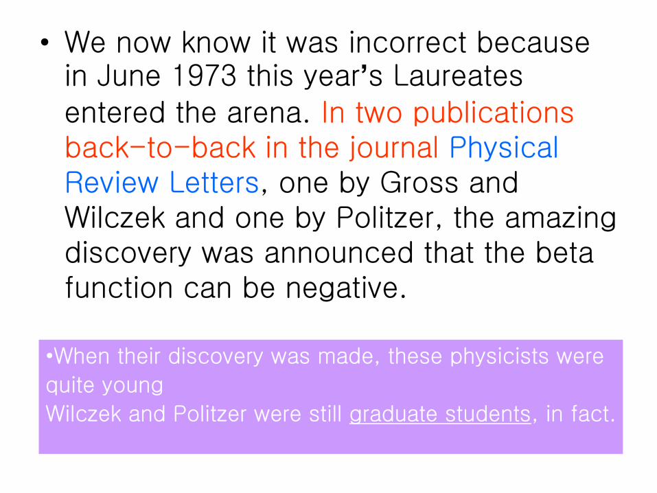
• We now know it was incorrect because in June 1973 this year’s Laureates entered the arena. In two publications back-to-back in the journal Physical Review Letters, one by Gross and Wilczek and one by Politzer, the amazing discovery was announced that the beta function can be negative.
•When their discovery was made, these physicists were
quite young
Wilczek and Politzer were still graduate students, in fact.

American citizen. Born 1951(53 years) in Queens, NY, USA. Doctor’s degree in physics in 1974 (23) at Princeton University. Professor at the Department of Physics at MIT, Cambridge MA, USA
Massachusetts Institute of Technology Center for Theoretical Physics77 Massachusetts Ave. 6-305 Cambridge, MA 02139USA
Frank A. Wilczek
American citizen. Born 1949(55 years). Doctor's degree in physics in 1974 (25) at Harvard University. Professor at the Department of Physics, California Institute of Technology (Caltech), Pasadena CA, USA.
California Institute of Technology,High Energy Physics452-48 Pasadena, CA 91106-3368USA
H. David Politzer
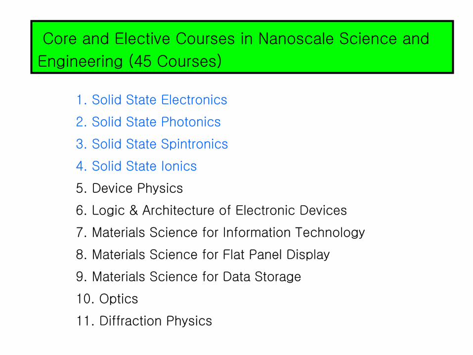
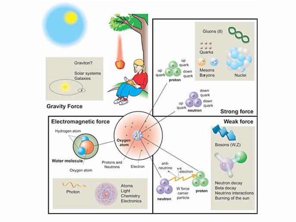
1. Solid State Electronics
2. Solid State Photonics
3. Solid State Spintronics
4. Solid State Ionics
5. Device Physics
6. Logic & Architecture of Electronic Devices
7. Materials Science for Information Technology
8. Materials Science for Flat Panel Display
9. Materials Science for Data Storage
10. Optics
11. Diffraction Physics
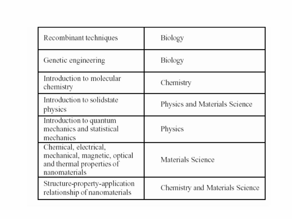
Core and Elective Courses in Nanoscale Science and
Engineering (45 Courses)

12. Materials for Extreme Engineering
13. Materials Science for Ferroelectric Materials
14. Milimeter Wave Materials
15. Mesoscopic Materials Science
16. Mechanical Properties of Solids
17. Electrochemistry of Solids
18. Basic Principles of Microprocessors
19. Physics of Non-volatile Memories
20. Materials Science for Artificial Bio Materials
21. Engineering for Microscopic Machines/MEMS/Actuators
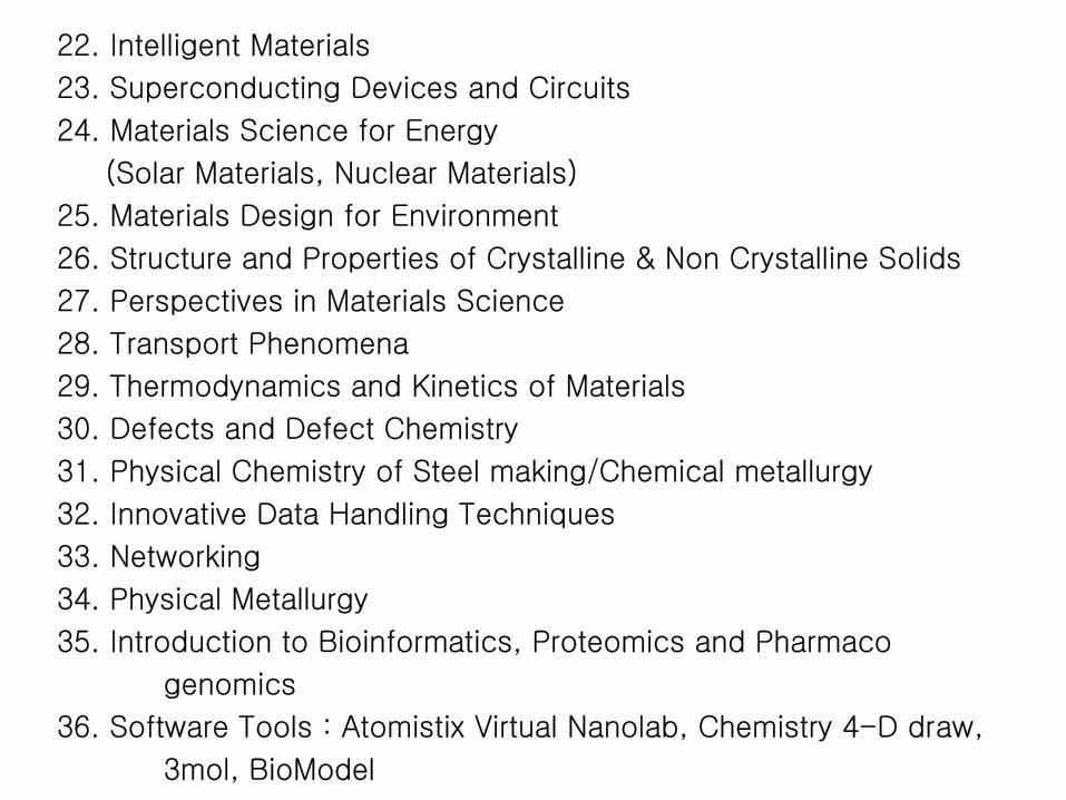
22. Intelligent Materials
23. Superconducting Devices and Circuits
24. Materials Science for Energy
(Solar Materials, Nuclear Materials)
25. Materials Design for Environment
26. Structure and Properties of Crystalline & Non Crystalline Solids
27. Perspectives in Materials Science
28. Transport Phenomena
29. Thermodynamics and Kinetics of Materials
30. Defects and Defect Chemistry
31. Physical Chemistry of Steel making/Chemical metallurgy
32. Innovative Data Handling Techniques
33. Networking
34. Physical Metallurgy
35. Introduction to Bioinformatics, Proteomics and Pharmaco
genomics
36. Software Tools : Atomistix Virtual Nanolab, Chemistry 4-D draw,
3mol, BioModel
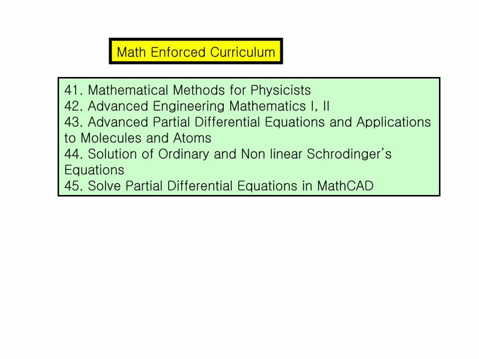
41. Mathematical Methods for Physicists42. Advanced Engineering Mathematics I, II43. Advanced Partial Differential Equations and Applications to Molecules and Atoms44. Solution of Ordinary and Non linear Schrodinger’sEquations45. Solve Partial Differential Equations in MathCAD
Math Enforced Curriculum
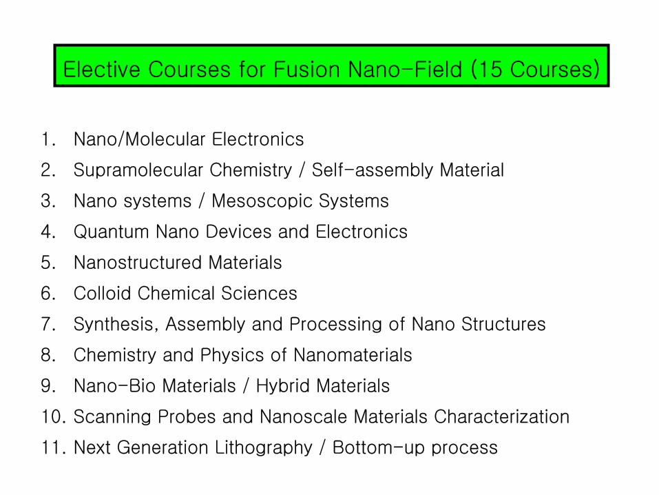
1. Nano/Molecular Electronics
2. Supramolecular Chemistry / Self-assembly Material
3. Nano systems / Mesoscopic Systems
4. Quantum Nano Devices and Electronics
5. Nanostructured Materials
6. Colloid Chemical Sciences
7. Synthesis, Assembly and Processing of Nano Structures
8. Chemistry and Physics of Nanomaterials
9. Nano-Bio Materials / Hybrid Materials
10. Scanning Probes and Nanoscale Materials Characterization
11. Next Generation Lithography / Bottom-up process
Elective Courses for Fusion Nano-Field (15 Courses)
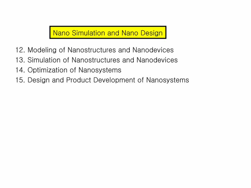
12. Modeling of Nanostructures and Nanodevices
13. Simulation of Nanostructures and Nanodevices
14. Optimization of Nanosystems
15. Design and Product Development of Nanosystems
Nano Simulation and Nano Design
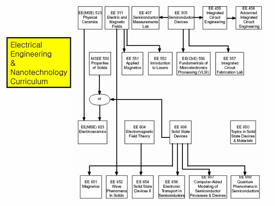
ElectricalEngineering&NanotechnologyCurriculum
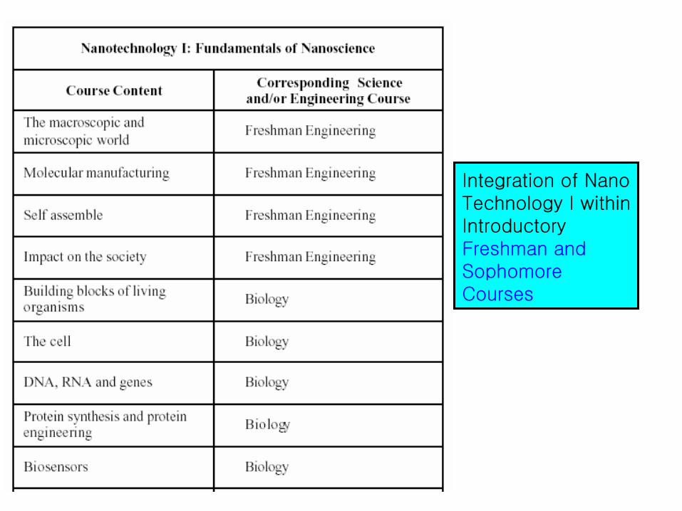
Integration of NanoTechnology I withinIntroductoryFreshman and SophomoreCourses

Integration of NanoTechnology II withinJunior and Senior Courses
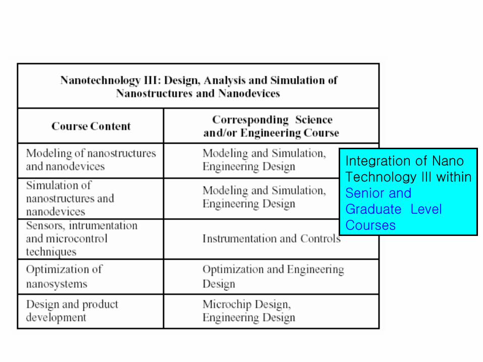
Integration of NanoTechnology III withinSenior and Graduate LevelCourses
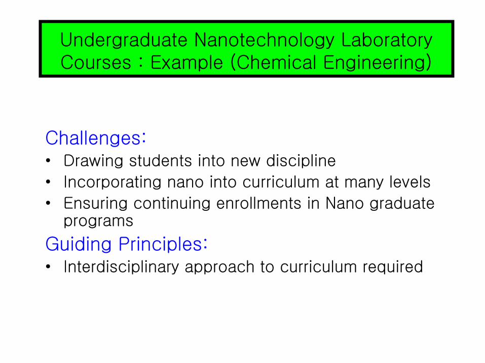
Challenges:• Drawing students into new discipline
• Incorporating nano into curriculum at many levels
• Ensuring continuing enrollments in Nano graduate programs
Guiding Principles:• Interdisciplinary approach to curriculum required
Undergraduate Nanotechnology Laboratory Courses : Example (Chemical Engineering)
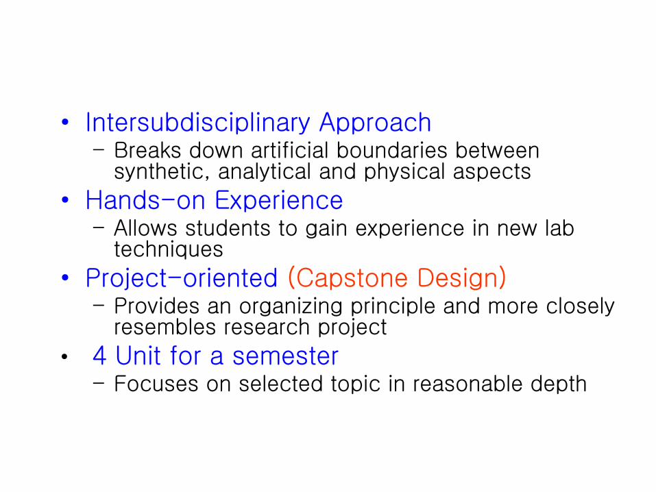
• Intersubdisciplinary Approach– Breaks down artificial boundaries between
synthetic, analytical and physical aspects
• Hands-on Experience– Allows students to gain experience in new lab
techniques
• Project-oriented (Capstone Design)– Provides an organizing principle and more closely
resembles research project
• 4 Unit for a semester– Focuses on selected topic in reasonable depth
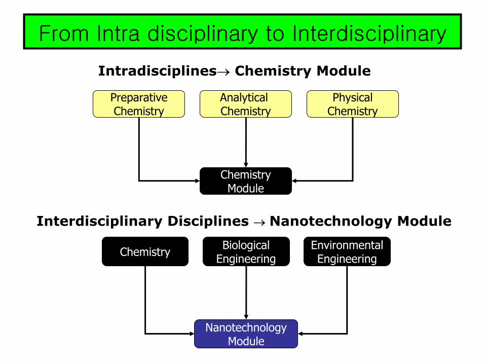
From Intra disciplinary to Interdisciplinary
ChemistryModule
PreparativeChemistry
Analytical Chemistry
PhysicalChemistry
Intradisciplines→ Chemistry Module
NanotechnologyModule
Chemistry BiologicalEngineering
EnvironmentalEngineering
Interdisciplinary Disciplines → Nanotechnology Module
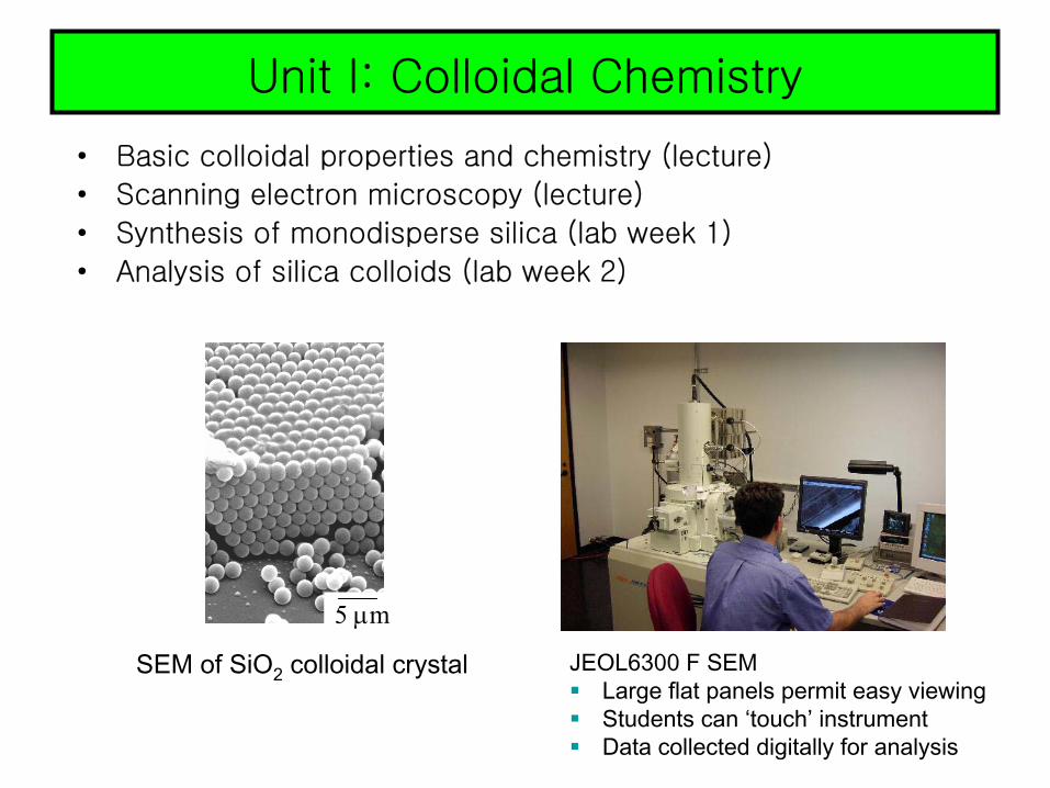
Unit I: Colloidal Chemistry
• Basic colloidal properties and chemistry (lecture)
• Scanning electron microscopy (lecture)
• Synthesis of monodisperse silica (lab week 1)
• Analysis of silica colloids (lab week 2)
JEOL6300 F SEMLarge flat panels permit easy viewingStudents can ‘touch’ instrument Data collected digitally for analysis
5 µm
SEM of SiO2 colloidal crystal

Unit II: Metal colloids/nanocrystals
JEOL 2010 TEMRoom for two to watch processHigh resolution imaging is possible/digital images
• Properties of metal colloids, historical uses (lecture)
• Chemistry and capping of gold nanocrystals (lecture)
• Transmission electron microscopy (lecture)
• Synthesis of gold nanocrystals-citrate method (lab week 2)
• Phase transfer method for gold nanocrystals and capping (lab week 3)
• Transmission electron microscopy of gold nanocrystals (lab week 4)
High resolution EM of TiO2nanocrystal
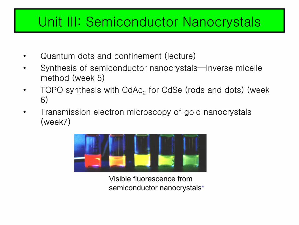
Unit III: Semiconductor Nanocrystals
• Quantum dots and confinement (lecture)
• Synthesis of semiconductor nanocrystals—Inverse micelle method (week 5)
• TOPO synthesis with CdAc2 for CdSe (rods and dots) (week 6)
• Transmission electron microscopy of gold nanocrystals(week7)
Visible fluorescence from semiconductor nanocrystals*

Unit IV : Fullerene Chemistry
Nd:YAG laser
Probephotodiode
Exc itation monitor
photodiode
FilterLens
λ/2 plate, filter
Sample cell
Beam flag
Beam stop
Dispersing prism
Diode laser
Beam sampler
Triplet Kinetics ApparatusOptical Schematic
• Isolation, Purification and Characterization– Soxhlet extraction of
fullerenes from soot– HPLC separation of C60 and
C70
– UV-vis spectrophotometry– Mass Spectrometry– 13C NMR Spectrometry
• Electrochemistry– Cyclic Voltammetry and
Differential Pulse Voltammetry
• Photophysics– Triplet decay Kinetics via
Flash Photolysis
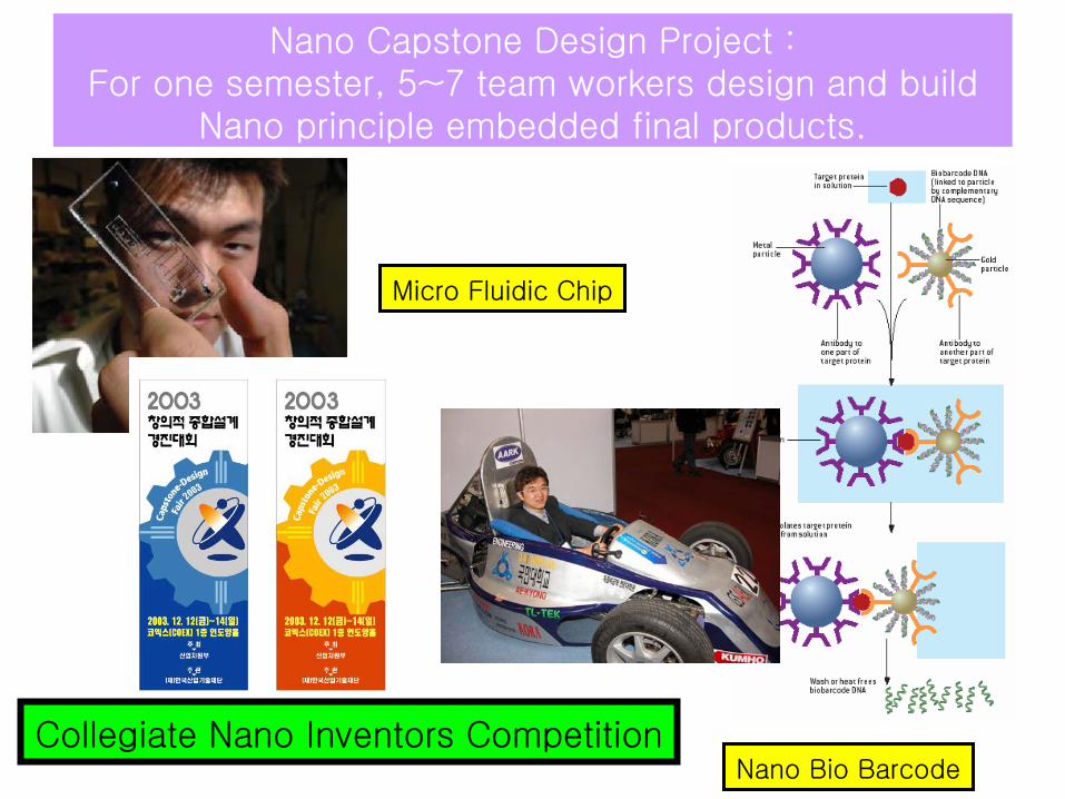
Nano Capstone Design Project :For one semester, 5~7 team workers design and build
Nano principle embedded final products.
Nano Bio Barcode
Micro Fluidic Chip
Collegiate Nano Inventors Competition
인천
대우전자GM 대우INI Steel
안양 수원
기흥
오산
평택천안
용인
서산(대산)
온양청주
대전
익산
광주
나주
광양
여수
구미 포항
창원 김해 부산
온산
울산
LG Philips
삼성전자삼성전기SKCKCC
대우전자
삼성전자
LG 전자
화성현대모비스 이천
하이닉스
LG 전자현대모비스
LG 화학 삼성전자
삼성전자삼성 SDISK 텔레텍SKC현대모비스
LG 전자LG 화학하이닉스
삼성전기
삼성전자LG 전자LG philips하이닉스대우전자
LG 화학
LG 화학대우전자삼성전자
LG 화학
POSCO
LG 화학
POSCOINI Steel
LG 전자LG 전자
삼성전기르노삼성
LG 화학
SK ㈜LG 화학현대자동차현대중공업
여주
KCC
생명공학연구소KAIST 뇌과학센터충남대의대LG 생명과학Bio Venture
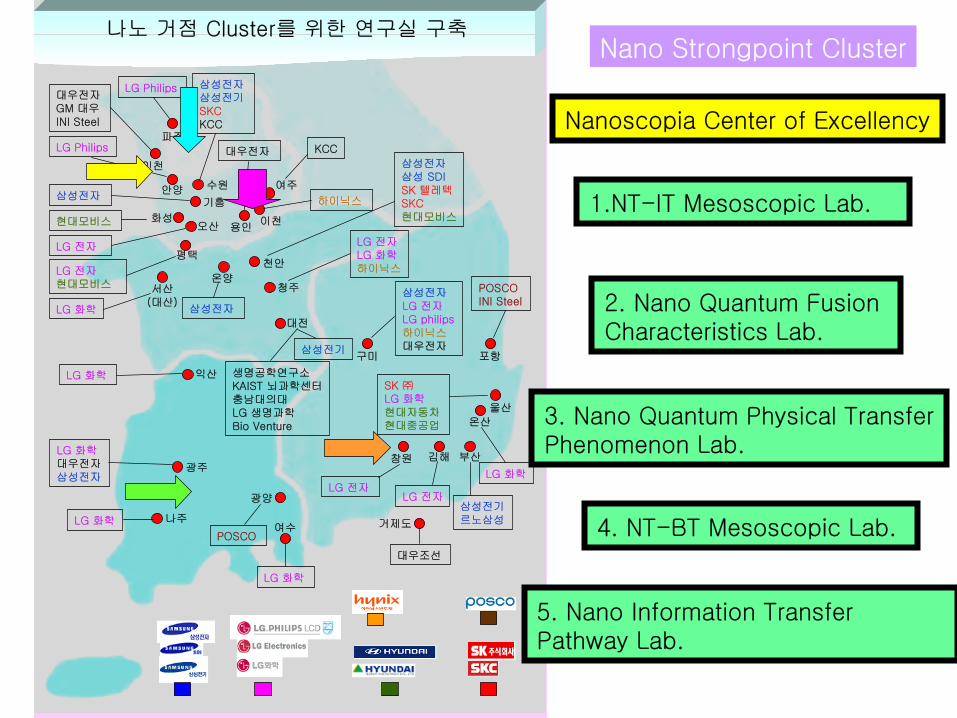
나노 거점 Cluster를 위한 연구실 구축
파주
LG Philips
대우조선
거제도
1.NT-IT Mesoscopic Lab.
2. Nano Quantum Fusion Characteristics Lab.
3. Nano Quantum Physical TransferPhenomenon Lab.
4. NT-BT Mesoscopic Lab.
5. Nano Information Transfer Pathway Lab.
Nanoscopia Center of Excellency
Nano Strongpoint Cluster
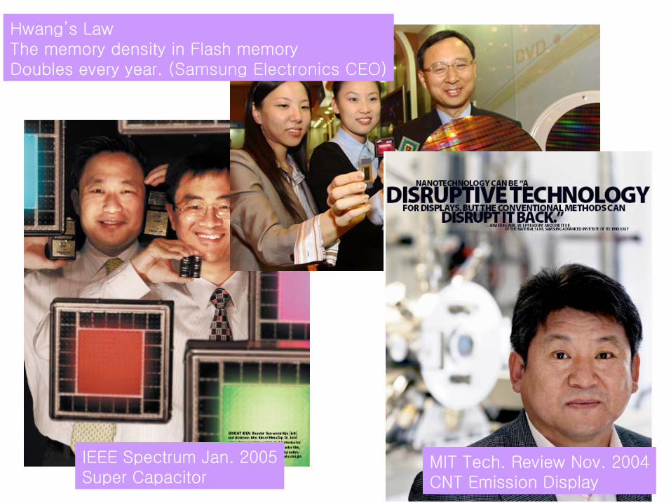
Hwang’ s Law
IEEE Spectrum Jan. 2005Super Capacitor
MIT Tech. Review Nov. 2004CNT Emission Display
Hwang’s LawThe memory density in Flash memoryDoubles every year. (Samsung Electronics CEO)
Thank you very much!!