Embed Size (px)
Citation preview

Planar GaAs Nanowires on GaAs (100)Substrates: Self-Aligned, NearlyTwin-Defect Free, and Transfer-PrintableSeth A. Fortuna,† Jianguo Wen,‡ Ik Su Chun,† and Xiuling Li*,†
Department of Electrical and Computer Engineering, Micro and NanotechnologyLaboratory, Frederick-Seitz Materials Research Laboratory, UniVersity of Illinois atUrbana-Champaign, Urbana, Illinois 61801
Received July 31, 2008; Revised Manuscript Received October 13, 2008
ABSTRACT
We report the controlled growth of planar GaAs semiconductor nanowires on (100) GaAs substrates using atmospheric pressure metalorganicchemical vapor deposition with Au as catalyst. These nanowires with uniform diameters are self-aligned in <110> direction in the plane of(100). The dependence of planar nanowire morphology and growth rate as a function of growth temperature provides insights into the growthmechanism and identified an ideal growth window of 470 ( 10 °C for the formation of such planar geometry. Transmission electron microscopyimages reveal clear epitaxial relationship with the substrate along the nanowire axial direction, and the reduction of twinning defect densityby about 3 orders of magnitude compared to <111> III-V semiconductor nanowires. In addition, using the concept of sacrificial layers andelevation of Au catalyst modulated by growth condition, we demonstrate for the first time a large area direct transfer process for nanowiresformed by a bottom-up approach that can maintain both the position and alignment. The planar geometry and extremely low level of crystalimperfection along with the transferability could potentially lead to highly integrated III-V nanoelectronic and nanophotonic devices on siliconand flexible substrates.
Semiconductor nanowires have been extensively studied inthe past decade for applications in nanoelectronics andnanophotonics. The bottom-up approach through metal-catalyzed growth allows for the routine synthesis of nanom-eter-scale devices and the flexibility to form functionalheterostructures with materials that are otherwise incompat-ible as thin films. To date, many classes of photonic andelectronic devices have been demonstrated including electri-cally pumped lasers, light-emitting diodes, photodetectors,field effect transistors, and logic gates.1-3 III-V semicon-ductor nanowires are of particular interest because of theirdirect bandgap, high carrier mobility, and ability to formheterojunctions. However, the abundance of twin-planedefects has been widely reported,4,5 which degrade the opticaland electronic properties. Wafer-scale integration with currentplanar processing technology remains a challenge for thecommonly grown out-of-plane nanowire geometry.3,6 Ex situassembly methods are required to transfer and coarsely alignthe nanowires in plane on a functional device substrate, butwithout control of the position of individual nanowires on awafer scale.7-11 More traditional top-down methods have
alternatively been successfully used to transfer semiconductormicro/nano wires to dissimilar substrates.12,13
The most widely reported process of semiconductornanowire growth is the vapor-liquid-solid (VLS)14 or therecently discovered vapor-solid-solid (VSS)15,16 mecha-nism. The driving force for crystallization is the supersatu-ration of liquid or solid alloy droplets which are formed bymetal catalytic absorption of gas reactants. The diametersof the nanowires are determined by the size of the seedparticles, while the growth direction has largely been reportedto depend on the surface free energy.17 It has been shownfor III-V materials with a cubic lattice that the lowest freeenergy surface is (111)B and thus nanowires grown on(111)B substrates are vertically aligned and perpendicularto the substrate.18 When (100) substrates are used, mostnanowires still grow in the <111>B direction, which is 35.3°angled from the substrate.18 Other growth directions havebeen observed sporadically during nanowire growth, presum-ably due to modification of free energy by strain, surfacetension etc.,17,19-24 and such nanowires have reportedlyshown fewer twinning defects.17 Promising results of planar<110> GaAs nanowire growth has been shown previously;however the length of the nanowires was limited to about500 nm (before the growth direction changed) and controlof the yield of planar nanowires through modulation ofgrowth conditions was not addressed.20 Recently, the self-
* To whom correspondence should be addressed. E-mail: [email protected].† Department of Electrical and Computer Engineering, Micro and
Nanotechnology Laboratory.‡ Frederick-Seitz Materials Research Laboratory.
NANOLETTERS
2008Vol. 8, No. 12
4421-4427
10.1021/nl802331m CCC: $40.75 2008 American Chemical SocietyPublished on Web 11/12/2008

alignment of horizontal ZnO nanowires on an a-planesapphire substrate using phase transport process through thecontrol of catalyst size and spacing22,25 has been reported.
In this research letter, we report a method that enablescontrolled large area growth of self-aligned planar <110>GaAs nanowires on GaAs (100) substrates using metalor-ganic chemical vapor deposition (MOCVD). As confirmedby transmission electron microscopy (TEM), the nanowireshave a zinc-blende crystal lattice and are mostly free of twin-plane defects for nanowires as long as 6 µm. A systematicgrowth study shows that the morphology and yield of theplanar nanowires can be controlled primarily through thegrowth temperature. In addition, by growing the planarnanowires on a sacrificial layer we demonstrate the possibilityof parallel transfer of the highly aligned planar nanowiresto a foreign substrate. The nanowires discussed in this letterwere grown with a Thomas Swan atmospheric pressureMOCVD reactor. Trimethylgallium (TMGa) and arsine(AsH3) were used as the gallium and arsenic precursors,respectively. Typical AsH3 flow was 200-500 sccm andTMGa was at 10 sccm (36-90 V/III molar ratio). GaAs(100) substrates were degreased and subsequently treatedwith diluted hydrochloric acid (HCl) to remove the nativeoxide. Colloidal gold (Au) nanoparticles with 5-20 nmnominal diameters were then directly deposited on thesubstrate (the substrates were not treated with an adhesionlayer such as poly-L-lysine). After colloidal gold deposition,the samples were transported to the MOCVD reactor andannealed at 620 °C under AsH3 flow for 10 min. This stepserved to alloy the Au with the GaAs substrate and desorbany residual native oxide. The temperature was ramped downto the growth temperature (420-520 °C) and TMGa wassubsequently introduced into the reactor. After the growth,samples were cooled under AsH3 flow. Nanowire length andmorphology were analyzed with a Hitachi 4800 scanningelectron microscope (SEM) at 15 kV.
Shown in Figures 1a-c are SEM images of as grownGaAs nanowires catalyzed using Au nanoparticles at 460-475°C under the conditions described above. The nanowires areself-aligned in plane in either the [1-10] or [-110] direction(Figure 1c) axially, and the radial cross-section appears tobe in a half-cylindrical shape. Nanowires that are 30 nm orsmaller in diameter exhibit smooth sidewall morphology.Few larger nanowires as large as 500 nm in diameter arealso observed and probably resulted from the aggregationof Au nanoparticles during dispersion and annealing steps.The large ones display distinct crystal facets on the wiresidewalls but the orientation is still in-plane along the two<110> directions.
Planar <110> nanowires almost completely disappear atlower temperatures (Figure 2a) and are replaced by mostlyangled <111> nanowires. In contrast, at higher growthtemperatures (Figure 2b), well-aligned in-plane triangularshapes (appear like “school of tadpoles”) are observed withthe apex of each triangle terminated with a Au nanoparticle.The top surface of the triangular wire is (001) while thesidewall facets of the triangles appear to be {111}. Thelengths of these triangular planar wires are noticeably shorter
than those cylindrical planar nanowires at 460 °C. Weattribute the shape of these triangular wires to the simulta-neous growth along the Au-catalyzed VLS nanowire growthdirection <110>, and the temperature enhanced nanowiresidewall growth. The sidewall growth apparently suppressesthe VLS growth, leading to lower axial growth rate. This isanalogous to the tapered vertical nanowire growth on (111)Bsubstrates, where a wider base in contact with the substrateand narrower top were formed at elevated temperatures andlonger growth time.26
Clearly, temperature, a well-controllable growth parameter,can be modulated to change the nanowire growth direction.Shown in Figure 3 is an Arrhenius plot of the planar axial
Figure 1. Planar <110> GaAs nanowires grown on GaAs (100)substrate. (a) Low, (b) medium, and (c) high magnification SEMimages of well-aligned <110> planar nanowires. Nanowires weregrown at 460 °C in (a,b) and at 475 °C in (c). Sample is not tiltedin (a) and tilted 75° in (b,c).
4422 Nano Lett., Vol. 8, No. 12, 2008
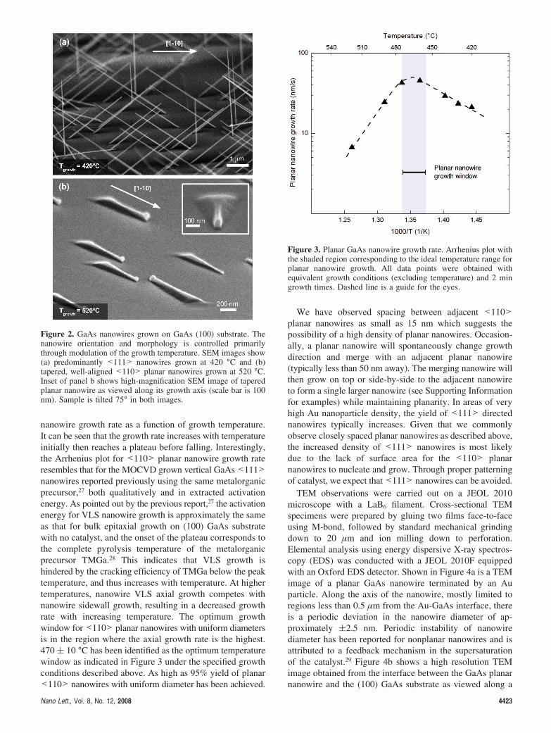
nanowire growth rate as a function of growth temperature.It can be seen that the growth rate increases with temperatureinitially then reaches a plateau before falling. Interestingly,the Arrhenius plot for <110> planar nanowire growth rateresembles that for the MOCVD grown vertical GaAs <111>nanowires reported previously using the same metalorganicprecursor,27 both qualitatively and in extracted activationenergy. As pointed out by the previous report,27 the activationenergy for VLS nanowire growth is approximately the sameas that for bulk epitaxial growth on (100) GaAs substratewith no catalyst, and the onset of the plateau corresponds tothe complete pyrolysis temperature of the metalorganicprecursor TMGa.28 This indicates that VLS growth ishindered by the cracking efficiency of TMGa below the peaktemperature, and thus increases with temperature. At highertemperatures, nanowire VLS axial growth competes withnanowire sidewall growth, resulting in a decreased growthrate with increasing temperature. The optimum growthwindow for <110> planar nanowires with uniform diametersis in the region where the axial growth rate is the highest.470 ( 10 °C has been identified as the optimum temperaturewindow as indicated in Figure 3 under the specified growthconditions described above. As high as 95% yield of planar<110> nanowires with uniform diameter has been achieved.
We have observed spacing between adjacent <110>planar nanowires as small as 15 nm which suggests thepossibility of a high density of planar nanowires. Occasion-ally, a planar nanowire will spontaneously change growthdirection and merge with an adjacent planar nanowire(typically less than 50 nm away). The merging nanowire willthen grow on top or side-by-side to the adjacent nanowireto form a single larger nanowire (see Supporting Informationfor examples) while maintaining planarity. In areas of veryhigh Au nanoparticle density, the yield of <111> directednanowires typically increases. Given that we commonlyobserve closely spaced planar nanowires as described above,the increased density of <111> nanowires is most likelydue to the lack of surface area for the <110> planarnanowires to nucleate and grow. Through proper patterningof catalyst, we expect that <111> nanowires can be avoided.
TEM observations were carried out on a JEOL 2010microscope with a LaB6 filament. Cross-sectional TEMspecimens were prepared by gluing two films face-to-faceusing M-bond, followed by standard mechanical grindingdown to 20 µm and ion milling down to perforation.Elemental analysis using energy dispersive X-ray spectros-copy (EDS) was conducted with a JEOL 2010F equippedwith an Oxford EDS detector. Shown in Figure 4a is a TEMimage of a planar GaAs nanowire terminated by an Auparticle. Along the axis of the nanowire, mostly limited toregions less than 0.5 µm from the Au-GaAs interface, thereis a periodic deviation in the nanowire diameter of ap-proximately (2.5 nm. Periodic instability of nanowirediameter has been reported for nonplanar nanowires and isattributed to a feedback mechanism in the supersaturationof the catalyst.29 Figure 4b shows a high resolution TEMimage obtained from the interface between the GaAs planarnanowire and the (100) GaAs substrate as viewed along a
Figure 2. GaAs nanowires grown on GaAs (100) substrate. Thenanowire orientation and morphology is controlled primarilythrough modulation of the growth temperature. SEM images show(a) predominantly <111> nanowires grown at 420 °C and (b)tapered, well-aligned <110> planar nanowires grown at 520 °C.Inset of panel b shows high-magnification SEM image of taperedplanar nanowire as viewed along its growth axis (scale bar is 100nm). Sample is tilted 75° in both images.
Figure 3. Planar GaAs nanowire growth rate. Arrhenius plot withthe shaded region corresponding to the ideal temperature range forplanar nanowire growth. All data points were obtained withequivalent growth conditions (excluding temperature) and 2 mingrowth times. Dashed line is a guide for the eyes.
Nano Lett., Vol. 8, No. 12, 2008 4423

<110> direction that is perpendicular to the nanowire growthdirection. The GaAs nanowire clearly extends the substratezinc-blende lattice epitaxially and the growth direction isalong the <110> direction. No apparent misfit dislocationsand only a few stacking faults have been found for the 5µm long nanowires examined, in contrast to the high densityof twin boundaries (∼5-10 nm in average spacing) reportedin GaAs <111> nanowires.4,30,31 This is an improvement oftwin defect density by about 3 orders of magnitude. Unlikethe <111> nanowires, the interface between the Au andGaAs for these planar <110> nanowires is not perpendicularto the growth direction. As shown in Figure 4c, the Aunanoparticle intercepts with GaAs at (001) and (110) facets,in addition, a well-defined (111) interface (35° angled fromthe growth direction) between Au nanoparticle and GaAs isactually formed. Observations of (111) interface betweenmetal catalyst nanoparticle and semiconductor have beenreported previously for non-<111> nanowires, presumablydue to its low interfacial energy. We have also observedanother type of Au-GaAs interface, as shown in Figure 4d,where the Au nanoparticle deformed to form mainly (110)and (001) interfaces with Au elevated on top of the long(001) facet. The composition analysis by EDS of Au particlesindicates a Ga composition of 5% or less. This is consistentwith continued precipitation of Ga out of the Au/Ga alloyto form GaAs due to the presence of AsH3 overpressureduring cooling down,15 which could result in different Au-GaAs interfaces due to the high mobility of Au particles.
It has been reported that the surface free energy could bemodified depending on nanowire density, and size (thus edgetension), substrate type and Au/Ga eutectic composi-tion.23,32-35 Although we did not study the nanowire sizeeffect systematically, we do not believe the formation of<110> planar nanowire on (100) substrate is size relatedbecause we have observed planar wires as small as 20 nmand as large as 500 nm in diameter. Close examination of
the nanowire initial growth region clearly shows an angledsidewall profile (not shown), implying <111> as the onsetnucleation direction. The dominant planar geometry for thetapered nanowires (Figure 2b) suggests that sidewall growthpromotes planar growth. Furthermore, a two step growthexperiment, where initial growth was carried out at 460 °Cfollowed by continued growth at 420 °C, yielded <110>planar nanowires. This confirms the critical role of theenergetics of the initial nucleation in determining thenanowire growth direction. We hypothesize that planarnanowire growth initiates in the angled <111> direction viaVLS mechanism, but becomes quickly (likely within a fewmonolayers) pinned to the (100) substrate due to growth fromthe acute angle sidewall; planar growth subsequently pro-ceeds by the Au catalyzed VLS mechanism.
As indicated by the TEM results, the planar nanowiresare epitaxially attached to the substrate. For certain applica-tions, it is desirable to have the nanowires detached fromthe growth substrate and transferred to a foreign substratesuch as silicon or flexible polymer. For out-of-plane nanow-ires, this is typically done by sonicating the nanowires fromthe growth substrate into a solution followed by dispersiononto a foreign substrate. However, achieving both thecontrolled positioning and alignment of transferred nanowireson a wafer scale has not been demonstrated. In our case,transfer of planar nanowires can be achieved by growingthe nanowires on a sacrificial layer epitaxially deposited onthe substrate; the nanowires can then be released from thesubstrate (while maintaining their position and alignment)by selectively removing the sacrificial layer. Thus we canexploit the as-grown alignment along the <110> directionand control the position of nanowires through patternedcatalyst. The released nanowires can then be transferred toa foreign substrate. For GaAs materials, the most commonlyused sacrificial layer AlxGa1-xAs (x g 0.5) is easily oxidizedin air and cannot be used as the surface for Au catalyst
Figure 4. TEM images of planar GaAs nanowires. (a) Low-magnification TEM image of <110> planar nanowire without stacking faults.(b) High-resolution TEM image of the nanowire-substrate interface. The top half of the nanowire delaminated during sample preparationand is not visible. The contrast at the nanowire-substrate interface is most likely from a thickness difference between the two regions. (c,d)TEM images of the two types of Au-GaAs interfaces observed. Insets show defect-free zinc-blende lattice (scale bars are both 2.5 nm).
4424 Nano Lett., Vol. 8, No. 12, 2008

deposition for subsequent planar nanowire growth. Instead,we have developed a method to grow the sacrificial layerafter the Au nanoparticles are deposited, which is schemati-cally illustrated in Figure 5a-d. Au nanoparticles were firstdeposited on the GaAs substrate (Figure 5a), which was thenannealed as described above. A thin (25-50 nm) sacrificialAl0.50Ga0.50As epilayer was grown at 625 °C to favornoncatalyzed overgrowth on the substrate. The Au nanopar-ticles were elevated under such growth condition above thesacrificial layer and onto the surface (Figure 5b). Thetemperature was then ramped down to 460 °C to favor Au-catalyzed growth and planar GaAs nanowires were grownon the Al0.50Ga0.50As epilayer (Figure 5c). The samples werecooled under AsH3 flow and removed from the MOCVDreactor. To release the GaAs nanowires from the substrate,the Al0.50Ga0.50As epilayer was wet etched and removed withaqueous HF (49% HF) (Figure 5d). Figure 5e,f shows theresult of such a process after the sacrificial layer(Al0.50Ga0.50As) is etched with HF to release the GaAsnanowires. The alignment of the nanowires clearly does notchange when they are released from the substrate.
The morphology and structural properties of GaAs nanow-ires grown on Al0.50Ga0.50As behaves identically to GaAsnanowires directly grown on a GaAs substrate. Using TEM,we have confirmed that GaAs nanowires grown on anAl0.50Ga0.50As sacrificial layer also have an extremely lowlevel of twin defects (see Supporting Information). Consider-ing the epitaxial relationship between the planar GaAsnanowire and growth substrate (see Figure 4b), this observa-tion is consistent with the negligible lattice constant mismatch
(0.07%) between GaAs and Al0.50Ga0.50As. In addition, thegrowth rates of GaAs nanowires grown on the sacrificiallayer (Al0.50Ga0.50As) and directly on GaAs substrate arenearly equivalent. However, for higher aluminum composi-tion AlxGa1-xAs layer, reduced nanowire growth rate (Au-catalyzed) is observed due to the competing overgrowth onhighly reactive AlxGa1-xAs (x > ∼0.55) surface. Theovergrowth also prevents clean release of nanowires insubsequent steps, making AlxGa1-xAs (x > 0.5) not suitableas sacrificial layers in this case.
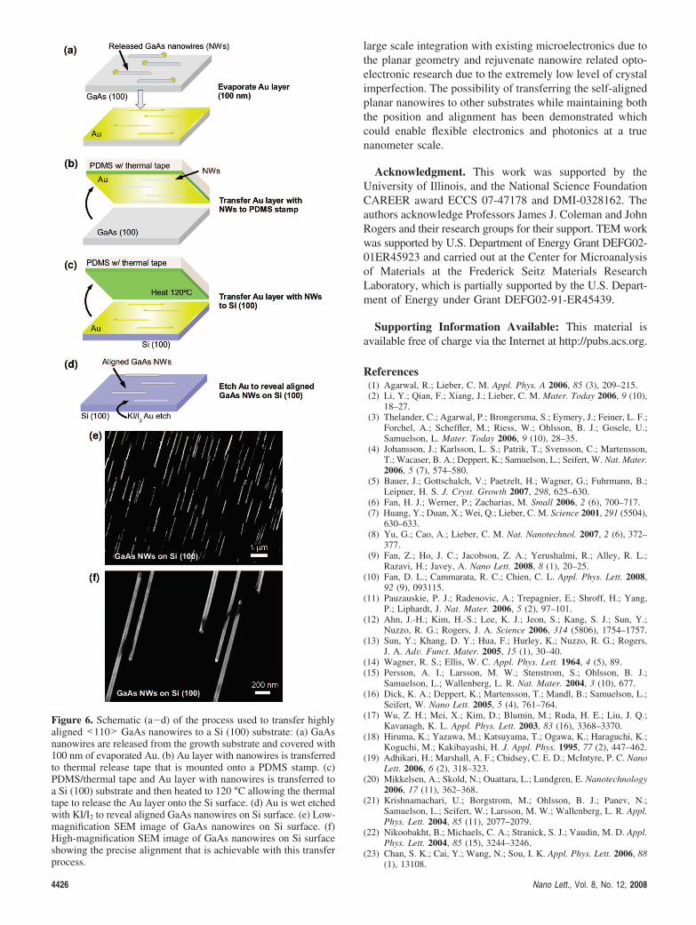
After the nanowires are released, they can readily be lift-off and transfer-printed to desired substrates. Using a similarprocess developed by other groups for the transfer of carbonnanotubes,36,37 we have successfully transferred the GaAsnanowires from their native growth substrate to a silicon(100) substrate with the process illustrated in Figure 6a-d.We first release GaAs nanowires from the growth substrateusing the procedure described in Figure 5 and then evaporatea 100 nm of Au onto the released nanowires (Figure 6a).Using thermal release tape (REVALPHA, Nitto Denko) thatis mounted on a poly(dimethylsiloxane) (PDMS) stamp, theAu layer together with the nanowires are then peeled offthe growth substrate (Figure 6b). Evaporated Au adherespoorly to the GaAs substrate surface, however the bondbetween the Au layer and released nanowires is strongenough such that the nanowires remain attached to the Aulayer during this step. The Au layer with nanowires is thentransferred to a bare silicon substrate and the entire assemblyis heated to 120 °C (Figure 6c). This heating will cause thethermal tape to lose its adhesion to the Au layer. The Auwith nanowires will then remain on the silicon surface afterthe PDMS stamp and thermal tape are removed from thesilicon (Figure 6d). Finally, the Au is removed with a 20 sKI/I2 (Transene) wet etch thus revealing the aligned nano-wires on the silicon surface. Figure 6e,f shows a SEM imageof planar GaAs nanowires that have been transferred to asilicon substrate. Most of the nanowires have clearlymaintained their alignment throughout the entire transferprocess. The discoloration of the silicon surface and nanow-ires evident in Figure 6e,f is from the Au etchant which tendsto leave behind a scum that is difficult to rinse away.Although here we demonstrate the transfer of planar nanow-ires to silicon, the same process can be used to transfer thenanowires to any substrate that can withstand a 120 °C bakeand Au wet etch. To the best of our knowledge, this is thefirst demonstration of a large area direct transfer process fornanowires formed by a bottom-up approach that can controlboth the position and alignment. Future work includespatterning the catalyst and controlling the growth direction([-110] or [1-10]) such that highly aligned arrays of position-controlled nanowires can be transferred.
In conclusion, self-aligned planar <110> GaAs nanowiresgrown by atmospheric pressure MOCVD on GaAs (100)substrates have been reported. The growth modes betweenplanar and angled nanowires can be modulated by growthtemperature. The temperature window for the planar nano-wire formation is ∼20 °C at the experimental conditionspecified. The reported research could potentially lead to
Figure 5. Schematic (a-d) of the process used to release planarGaAs nanowires from the growth substrate: (a) Au catalyst isdispersed on GaAs (100) substrate. (b) A thin (25-50 nm) sacrificialAl0.50Ga0.50As epilayer (blue colored) is grown at T ) 625 °C; Aucatalyst elevates above the sacrificial layer and onto the surface.(c) GaAs nanowires are grown at T ) 460 °C. (d) GaAs nanowiresare released when Al0.50Ga0.50As sacrificial layer (blue colored) isremoved with HF. (e) SEM image of released GaAs nanowires.The nanowires clearly remain aligned. (f) SEM image of a nanowirethat is partially released from the substrate (arrow points to theremaining sacrificial layer).
Nano Lett., Vol. 8, No. 12, 2008 4425
large scale integration with existing microelectronics due tothe planar geometry and rejuvenate nanowire related opto-electronic research due to the extremely low level of crystalimperfection. The possibility of transferring the self-alignedplanar nanowires to other substrates while maintaining boththe position and alignment has been demonstrated whichcould enable flexible electronics and photonics at a truenanometer scale.
Acknowledgment. This work was supported by theUniversity of Illinois, and the National Science FoundationCAREER award ECCS 07-47178 and DMI-0328162. Theauthors acknowledge Professors James J. Coleman and JohnRogers and their research groups for their support. TEM workwas supported by U.S. Department of Energy Grant DEFG02-01ER45923 and carried out at the Center for Microanalysisof Materials at the Frederick Seitz Materials ResearchLaboratory, which is partially supported by the U.S. Depart-ment of Energy under Grant DEFG02-91-ER45439.
Supporting Information Available: This material isavailable free of charge via the Internet at http://pubs.acs.org.
References(1) Agarwal, R.; Lieber, C. M. Appl. Phys. A 2006, 85 (3), 209–215.(2) Li, Y.; Qian, F.; Xiang, J.; Lieber, C. M. Mater. Today 2006, 9 (10),
18–27.(3) Thelander, C.; Agarwal, P.; Brongersma, S.; Eymery, J.; Feiner, L. F.;
Forchel, A.; Scheffler, M.; Riess, W.; Ohlsson, B. J.; Gosele, U.;Samuelson, L. Mater. Today 2006, 9 (10), 28–35.
(4) Johansson, J.; Karlsson, L. S.; Patrik, T.; Svensson, C.; Martensson,T.; Wacaser, B. A.; Deppert, K.; Samuelson, L.; Seifert, W. Nat. Mater.2006, 5 (7), 574–580.
(5) Bauer, J.; Gottschalch, V.; Paetzelt, H.; Wagner, G.; Fuhrmann, B.;Leipner, H. S. J. Cryst. Growth 2007, 298, 625–630.
(6) Fan, H. J.; Werner, P.; Zacharias, M. Small 2006, 2 (6), 700–717.(7) Huang, Y.; Duan, X.; Wei, Q.; Lieber, C. M. Science 2001, 291 (5504),
630–633.(8) Yu, G.; Cao, A.; Lieber, C. M. Nat. Nanotechnol. 2007, 2 (6), 372–
377.(9) Fan, Z.; Ho, J. C.; Jacobson, Z. A.; Yerushalmi, R.; Alley, R. L.;
Razavi, H.; Javey, A. Nano Lett. 2008, 8 (1), 20–25.(10) Fan, D. L.; Cammarata, R. C.; Chien, C. L. Appl. Phys. Lett. 2008,
92 (9), 093115.(11) Pauzauskie, P. J.; Radenovic, A.; Trepagnier, E.; Shroff, H.; Yang,
P.; Liphardt, J. Nat. Mater. 2006, 5 (2), 97–101.(12) Ahn, J.-H.; Kim, H.-S.; Lee, K. J.; Jeon, S.; Kang, S. J.; Sun, Y.;
Nuzzo, R. G.; Rogers, J. A. Science 2006, 314 (5806), 1754–1757.(13) Sun, Y.; Khang, D. Y.; Hua, F.; Hurley, K.; Nuzzo, R. G.; Rogers,
J. A. AdV. Funct. Mater. 2005, 15 (1), 30–40.(14) Wagner, R. S.; Ellis, W. C. Appl. Phys. Lett. 1964, 4 (5), 89.(15) Persson, A. I.; Larsson, M. W.; Stenstrom, S.; Ohlsson, B. J.;
Samuelson, L.; Wallenberg, L. R. Nat. Mater. 2004, 3 (10), 677.(16) Dick, K. A.; Deppert, K.; Martensson, T.; Mandl, B.; Samuelson, L.;
Seifert, W. Nano Lett. 2005, 5 (4), 761–764.(17) Wu, Z. H.; Mei, X.; Kim, D.; Blumin, M.; Ruda, H. E.; Liu, J. Q.;
Kavanagh, K. L. Appl. Phys. Lett. 2003, 83 (16), 3368–3370.(18) Hiruma, K.; Yazawa, M.; Katsuyama, T.; Ogawa, K.; Haraguchi, K.;
Koguchi, M.; Kakibayashi, H. J. Appl. Phys. 1995, 77 (2), 447–462.(19) Adhikari, H.; Marshall, A. F.; Chidsey, C. E. D.; McIntyre, P. C. Nano
Lett. 2006, 6 (2), 318–323.(20) Mikkelsen, A.; Skold, N.; Ouattara, L.; Lundgren, E. Nanotechnology
2006, 17 (11), 362–368.(21) Krishnamachari, U.; Borgstrom, M.; Ohlsson, B. J.; Panev, N.;
Samuelson, L.; Seifert, W.; Larsson, M. W.; Wallenberg, L. R. Appl.Phys. Lett. 2004, 85 (11), 2077–2079.
(22) Nikoobakht, B.; Michaels, C. A.; Stranick, S. J.; Vaudin, M. D. Appl.Phys. Lett. 2004, 85 (15), 3244–3246.
(23) Chan, S. K.; Cai, Y.; Wang, N.; Sou, I. K. Appl. Phys. Lett. 2006, 88(1), 13108.
Figure 6. Schematic (a-d) of the process used to transfer highlyaligned <110> GaAs nanowires to a Si (100) substrate: (a) GaAsnanowires are released from the growth substrate and covered with100 nm of evaporated Au. (b) Au layer with nanowires is transferredto thermal release tape that is mounted onto a PDMS stamp. (c)PDMS/thermal tape and Au layer with nanowires is transferred toa Si (100) substrate and then heated to 120 °C allowing the thermaltape to release the Au layer onto the Si surface. (d) Au is wet etchedwith KI/I2 to reveal aligned GaAs nanowires on Si surface. (e) Low-magnification SEM image of GaAs nanowires on Si surface. (f)High-magnification SEM image of GaAs nanowires on Si surfaceshowing the precise alignment that is achievable with this transferprocess.
4426 Nano Lett., Vol. 8, No. 12, 2008

(24) Song, M. S.; Jung, J. H.; Kim, Y.; Wang, Y.; Zou, J.; Joyce, H. J.;Gao, Q.; Tan, H. H.; Jagadish, C. Nanotechnology 2008, 19 (12),125602.
(25) Nikoobakht, B. Chem. Mater. 2007, 19 (22), 5279.(26) Plante, M. C.; LaPierre, R. R. J. Cryst. Growth 2008, 310 (2), 356–63.(27) Borgstrom, M.; Deppert, K.; Samuelson, L.; Seifert, W. J. Cryst.
Growth 2004, 260 (1-2), 18–22.(28) Larsen, C. A.; Li, S. H.; Buchan, N. I.; Stringfellow, G. B.; Brown,
D. W. J. Cryst. Growth 1990, 102 (1-2), 126–136.(29) Kohno, H.; Takeda, S. J. Cryst. Growth 2000, 216 (1-4), 185–191.(30) Xiong, Q.; Wang, J.; Eklund, P. C. Nano Lett. 2006, 6 (12), 2736.(31) Davidson, F. M., III; Lee, D. C.; Fanfair, D. D.; Korgel, B. A. J.
Phys. Chem. C 2007, 7, 2929–2935.
(32) Ihn, S. G.; Song, J. I.; Kim, Y. H.; Lee, J. Y. Appl. Phys. Lett. 2006,89 (5), 53106.
(33) Yuan, C.; Siu Keung, C.; Iam Keong, S.; Yu Fai, C.; Su, D. S.; Ning,W. Small 2007, 3 (1), 111.
(34) Yue, W.; Yi, C.; Lynn, H.; Barrelet, C. J.; Bell, D. C.; Lieber, C. M.Nano Lett. 2004, 4 (3), 433.
(35) Schmidt, V.; Senz, S.; Gosele, U. Nano Lett. 2005, 5 (5), 931.(36) Seung-Hyun, H.; Park, O. O.; John, A. R. Appl. Phys. Lett. 2005, 86
(24), 243502.(37) Chuan, W.; Koungmin, R.; Alexander, B.; Nishant, P.; Albert, L.;
Subhasish, M.; Wong, H. S. P.; Chongwu, Z. Appl. Phys. Lett. 2008,93 (3), 033101.
NL802331M
Nano Lett., Vol. 8, No. 12, 2008 4427

![Metal-catalyzed semiconductor nanowires · Axial and radial impurity doping for both n-type ... 110 a comprehensive list 112 a GaAs 111 Ba/[0001] ... (a)(b) (c)(d) (e)(f)](https://img.pdfslide.net/doc/110x75/5acbc8bf7f8b9a93268babf1/metal-catalyzed-semiconductor-nanowires-and-radial-impurity-doping-for-both-n-type.jpg)


![Field Emission from Self-Catalyzed GaAs Nanowires · One-dimensional pillars fabricated by the electrochemical etching of (111) GaAs substrate [33,34] resulted in a diameter (~2 m)](https://img.pdfslide.net/doc/110x75/602d27305d1f537330616710/field-emission-from-self-catalyzed-gaas-nanowires-one-dimensional-pillars-fabricated.jpg)


![Optical properties of heavily doped GaAs nanowires and ... · Nanowire EL structures have already been demonstrated in axial pn-junctions [3, 5] as well as in axial quantum well structures](https://img.pdfslide.net/doc/110x75/5f416b32f223013ea10ccf0a/optical-properties-of-heavily-doped-gaas-nanowires-and-nanowire-el-structures.jpg)