Embed Size (px)
Citation preview
Nano-optical Spectroscopy of Low Dimensional Semiconductor
By
Wei Bao
A dissertation submitted in partial satisfaction of the requirements for the degree of
Doctor of Philosophy
in
Engineering - Materials Science and Engineering
in the
Graduate Division
of the
University of California, Berkeley
Committee in charge:
Professor Miquel Salmeron, Co-Chair
Professor Ting Xu, Co-Chair
Professor Eli Yablonovitch
Professor Peidong Yang
Spring 2015
Nano-optical Spectroscopy of Low Dimensional Semiconductor
Copyright 2015
By
Wei Bao
1
Abstract
Nano-optical Spectroscopy of Low Dimensional Semiconductor
Wei Bao
Doctor of Philosophy in Materials Science and Engineering
University of California, Berkeley
Professor Miquel Salmeron, Chair
The necessity to push the spatial resolution of optical microscopy and spectroscopy beyond the diffraction limit has been of high interest for almost three decades starting with the idea of using an aperture smaller than the diffraction limit by Ash and Nicholls (Nature 237, 510 – 512) and first examples on nano spectroscopy by Betzig and Trautman (Science 257, 189-195), who advertised: “two of the most exciting possibilities are localized optical spectroscopy of semiconductors and fluorescence imaging of living cells”. However, albeit its enormous potential for the advancement of nano science to study at the critical length scales physical and chemical properties of nano materials that can be accessed only optically, nano optics has developed only a niche existence. The reasons are many limitations of present nano optics, which advanced specific aspects e.g. high local field intensity via the concept of optical antennae (Science 308, 1607-1609) but with major trade offs such as lack of band width, background of diffraction limited light or intrinsic geometries that enable only the study of e.g. monolayers of molecules squeezed between metal substrate and a metal tip. Here we present a wildly applicable solution to the nanoscale spectroscopy problem with the concept of a far-field to near field optical transformer that does not require the trade offs made in the past and combines record near field enhancement, enormous bandwidth, background free and complete sample independence to perform nano scale optical spectroscopy. The “campanile” transformer is the missing element that enables to perform the whole bandwidth of optical spectroscopy modalities. In the first part of this thesis, the finite element method is used compare the properties of this “campanile” structure with conventional aperture and apertureless NSOM tips, as well as state-of-the-art adiabatic-compression-type
2
probes. These benchmarks elucidate a number of advantages of the campanile design, showing that its unique characteristics are crucial for optical techniques such as nano-Raman and nano-IR spectroscopy and nano-photoluminescence studies.
In the second part of the thesis, we have experimentally used the campanile transformer to perform indeed local optical spectroscopy of semiconducting Indium Phosphite nanowires (InP NW),1D semiconductor, taking advantage of enhancement, bandwidth as well as the ability to excite and collect through the campanile, to show the influence of trap states on the local excitation energy and charge recombination rate. InP NWs have fascinating opto-electronic properties (Science 293, 1455-1457) and are expected to be the functional elements of next generation opto-electronic devices. However, many of the observed optical phenomena in nanowire systems are not understood due to the lack of spatial resolution. This work provides the necessary insight to start understanding the optical properties of nanowire and nano crystals systems. We demonstrate how the concept of optical campanile transformers convert bi-directional light with high efficiency between far and near field over a bandwidth spanning the visible to the near IR. Utilizing the campanile to perform hyperspectral nano optical spectroscopy on InP NWs revealed strong heterogeneity of the local photoluminescence, both in local intensity and spectral response, along individual NWs, due to the local influence of trap states.
In the last part of the thesis, we present the first nano-optical investigation of 2D transition metal dichalcogenides (TMDCs). Establishing a breakthrough solution to the “nanospectroscopy imaging” problem for these materials, we cross the boundary from insufficient to sufficient optical spatial resolution, mapping critical optoelectronic properties at their native length scales. In doing so, we uncover new optoelectronic regions and spatially-varying features in CVD-grown MoS2 that were hidden in prior optical studies. We discover an unexpected edge region in synthetic MoS2 (~300 nm wide) that acts as a collection of disordered states effectively localizing carriers and excitons. Moreover, we show that significant nanoscale optoelectronic heterogeneity is present even within more “conventional” regions, and directly visualize the optoelectronic effects of key features such defects and edges – highly-soughtafter information that was unobtainable previously. By revealing key structure-function relationships at the proper length scales, these findings directly impact nearly all anticipated atomically-thin device technologies including novel quantum-optical circuitry, bio sensors and valley-based electronics.

i
Dedicated to my family

ii
Table of Contents Abstract ............................................................................................................ 1
Table of Contents ............................................................................................. ii
Acknowledgements .......................................................................................... iii
Chapter 1 : Introduction .................................................................................... 1
Chapter 2 : Campanile probe: A in-depth theory comparison with other probes 5
Motivation and introduction ................................................................... 5
Materials and methods ......................................................................... 8
Results and discussions........................................................................ 9
Conclusion............................................................................................. 20
Chapter 3 : Mapping InP nanowires local charge recombination heterogeneity. 27
Motivation and introduction ................................................................... 27
Results and discussions ........................................................................ 32
Conclusion.............................................................................................. 38
Materials and methods ........................................................................... 39
Chapter 4 : Nano-optical spectroscopic imaging of monolayer MoS2.........…… 49
Motivation and introduction ..................................................................... 49
Results and discussions ......................................................................... 52
Conclusion .............................................................................................. 59
Materials and methods ........................................................................... 59
Chapter 5 : Conclusion and future work ............................................................ 77

iii
Acknowledgments
First, I would like to thank my advisor Prof. Miquel Salmeron for providing me the opportunity to work with him on this exciting project. I really appreciate his great vision, enthusiasm, and continuous support during the past years. I would want to thank the other advisor of mine Dr. P. James Schuck. I really appreciate his open mind when I chose a new topic to work on and his guidance, support and profound knowledge in the area of nano-optics. He is really my senior friends and will to defense and help me at all time. I want to express my thanks to my first mentor in experiment Dr. Alexander Weber-Bargioni. I could still remember the time we spent together in the cleanroom and the happiness we have when my first paper is accepted by Science. I wish him a great success in his future as a tenured scientist in LBNL. I would also like to take this opportunity to thank my thesis committee member Prof. Eli Yablonovitch. I always learnt a lot whenever I talked with Prof. Yablonovitch, his unique vision on metal-optics always help me go through the most difficult problem. Also without his early pioneering work on the optical transformer, it will be really hard to imagine I could finish this research. I would like to acknowledge Prof. Junqiao Wu, Prof. Ting Xu for chairing my qualify exam and my thesis respectively. I also enjoy a lot on the collaboration projects we have in the past years. I want to thank Prof. Peidong Yang for serving as one of my dissertation committee members as well. I would like take this opportunity to thank my colleague and friend, who is the most talent postdoc I have ever worked with in the past, Dr. Nicholas J. Borys, I learn about from him not only in the scientific side but also in the social aspect. We also generated the best scientific results, even not the best journal, in my Ph.D. together. I would like take this occasion to thank my colleagues, friends and collaborators: Ed Wong, Dr. Jiye Lee, Dr. Keiko Munechika, Dr. Francesca Intonti, Dr. Niccolo Caselli, Dr. Changhyun Ko, Prof. Sefaattin Tongay, Joonki Suh, Dr. Wen Fan, Dr. Deyi Fu, Dr. Chun Cheng, Dr. D. Frank Ogletree, Dr. Xiaofeng Feng, Dr. Zhongwei Zhu, Yingjie Zhang, Peter Bai, Sui Yang, Dr. Giuseppe Calafiore, Tianbo Sun, Prof. Connie Chang-Hasnain, Prof. Xiaogan Liang, Dr. Kibum Kang, Saien Xie, Prof. Jiwoong Park and David Hom. Specially thank to my parents Guosheng Bao and Shuqin Gao, for their endless love and support since the very first day I was born; my seven month old adorable daughter Amelia X. Bao, who pushes me a lot to work harder in the lab.

iv
Finally, I want to thank my dear wife Wenjun Shao, who married me without any hesitation at a time that I owed nothing and gave me a warm family ever since. She is an extremely good listener and always be on my side. She constantly tries her best to encourage me to pursue the most important scientific challenges.

v
Preface Being a productive graduate student is not easy, that is especially true, when I spent most of my time working in the Molecular Foundry, Lawrence Berkeley National Lab.
It is a place with many politics and non-scientific issues. Some of the time one will feel frustrated. On one hand, I feel I might potentially have access to the state of art instrumentations; on the other hand, there are many invisible nonscientific barriers on your way to solving the most frontier scientific questions. I was not always strong enough and smart enough to overcome these barriers.
Looking back into the past five years, I wish I could do a lot better, I wish I could have less struggle; I wish I could have more time focus on science. But the reality is cruel that most of the time one does not always get what they are deserved.
1
Chapter 1: Introduction
Visualizing object with better temporal and spatial resolution is a long-term challenge in science and technology. However, in the field optical microscopy and spectroscopy, it is extremely difficult to achieve spatial resolution below diffraction limit in a widely applicable fashion. Therefore, it is highly demanded that one can bring the spatial resolution of optical spectroscopy down to nanometer resolution and use it to probe the rich chemical and electronic states of material systems.
The fundamental diffraction limit physically comes from the wave nature of light.(1) In the traditional lens based system, the physical objectives which contain different spatial frequency information have to be propagate through medium (with refraction index n) and get focused on the imaging plane or detector. But the highest spatial frequency, which can propagate freely far away (longer than one wavelength) with exponential decay, can be written as:
0
2 2 nK π πλ λ
= =
Where K is the wave vector, 0λ is the vacuum wavelength. All the high frequency spatial information will be lost and, therefore, the best spatial resolution is
0.61. .N Aλ
, where . . sinN A n θ= × is the numerical aperture of the objective lens. A typical high quality air objective has a numerical aperture ~ 0.9. As an example, if one uses 632.8 nm laser light the best achievable spatial resolution is ~430 nm.
This is the fundamental limit of any lens-based imaging system. Traditionally, one simple way to improve the spatial resolution of the system is to use high refraction index materials. However, the transparent objective oil can only has a limited refraction index and, to date, most of the immersion lens system is using an immersion oil product with n around or below 2. The other way to push down the spatial resolution is to use shorter wavelength source, such as X-ray and electron beam. The major issues with these two techniques are sample damages and high vacuum requirements. Therefore, it is very challenging to get high-resolution optical imaging and ambient environment compatibility at the same time.
2
The first experimental approach to address this issue is aperture based near-field scanning optical microscopy (NSOM). The basic idea of NSOM is to collect the high spatial frequency signal at a near enough distance from samples, where they have not fully dies out. However, conventional aluminum coated tapered glass fiber probes, which serve as the central component of NSOM, has an extremely low throughput and weak intensity of light at the sample. For a typical 50 nm diameter probe, the transmission is only 10-5 – 10-6. Therefore, in order to get a decent signal to noise ratio, the spatial resolution of SNOM is typically limited at ~100 nm. This is because in a tapered glass fiber, when the size of core region shrinks gradually, propagating modes get cut-off one after another until the fundamental HE11 mode get cut-off at inner diameters <160 nm and only exponentially decayed evanescent waves leak out of the probe’s aperture(7). Suffering the transmission issue, the typical aperture based NSOM can only measure reflection or transmission of laser line and they cannot provide any optical spectral information, which contains both electronic and chemical information of the samples.
In 1994 a new approach(2), which is called apertureless NSOM (a-NSOM) nowadays, is proposed based on scattering from the apex of a sharp tip. The central element of the a-NSOM is a sharp smooth plasmonic metallic tip, typically made of silver or gold. When light illuminates from the side or bottom of the metallic sharp tip, due to the lightning rod and plasmonic effects, the electromagnetic field will be concentrated at the tip apex. The electric field direction near the tip will be mainly along z direction. The spatial resolution of images will be determined by the radius of the sharp tip instead of the incident wavelength. Many a-NSOM techniques have been developed including tip-enhanced Raman spectroscopy(3). Another configuration is to use STM to spatially both induce and map optical emission from specific orbitals of single molecules with angstrom resolution(4).
Using the most popular a-NSOM, researchers demonstrate a wide range of optical spectroscopy applications, including infrared plasmon and phonon imaging, single molecule TERS. But despite providing important information on material local chemical properties with ~10 nm, results from many a-NSOM experiments have proven inconsistent. This is because a-NSOM measurement is highly depends on the tip apex condition. In another word, the metallic tip apex shape and roughness will strongly affect the final electric field enhancement. Another issue is high electric field enhancement can be only achieved with a plasmonic substrate in STM mode. Therefore, in ambient dielectric substrate condition the only reliable measurement is still the scattering imaging of laser line signal.

3
The thesis present here is to solve the NSOM challenge mentioned above and bring a wildly applicable solution to the nanoscale spectroscopy problem in a way that does not require tradeoffs made in the past.

4
Reference 1. J. B. Pendry, Negative refraction makes a perfect lens. Physical Review
Letters 85, 3966-3969 (2000). 2. F. Zenhausern, M. P. Oboyle, H. K. Wickramasinghe, Apertureless near-
Field Optical Microscope. Applied Physics Letters 65, 1623-1625 (1994). 3. R. M. Stockle, Y. D. Suh, V. Deckert, R. Zenobi, Nanoscale chemical
analysis by tip-enhanced Raman spectroscopy. Chem Phys Lett 318, 131-136 (2000).
4. S. W. Wu, G. V. Nazin, W. Ho, Intramolecular photon emission from a single molecule in a scanning tunneling microscope. Physical Review B 77, (2008).
5
Chapter 2: Campanile probe: A in-depth theory comparison with other probes
Most of the work described in this chapter was published in
Optics express 21 (7), 8166-8176, 2013
Introduction and Motivation
The design of advanced nanostructured materials can benefit from spectroscopic characterization techniques that provide chemical information with nanoscale spatial resolution. In principle, optical near-field investigations can access this parameter space, but despite offering optical imaging and spectroscopy capabilities with sub-diffraction-limited resolution (1–8), the general applicability of near-field microscopy has been limited by the far-field to near-field coupling properties of its probes. A novel near-field probe structure (9,10) – known as the “campanile” geometry – based on a design originally proposed by Staffaroni and Yablonovitch (11) has recently been shown to enable multidimensional nanospectroscopic imaging of nanostructures without many of the constraints and limitations encountered by previous near-field probes (9). To better understand the capabilities of the campanile probe geometry, it is important to compare its optical properties with those of other near-field probes, which is the main focus of this Chapter.
An ideal near-field probe should possess nanoscale resolution, efficient far-field to nearfield coupling, strong local field enhancement, and perhaps most importantly, reproducibility and robustness. In addition, such a probe should provide background-free operation, control over near-field polarization, and operate over a wide range of frequencies (i.e. – it should be broadband rather than resonant). Compatibility with existing instrumentation would also be desirable. Conventional aperture-based near-field scanning optical microscopy (NSOM) tips are lacking in a number of these categories. This, combined with the increased need to characterize materials at nm length scales, has led in recent years to a number of approaches aimed at improving one or more of these desired near-field probe properties.
6
One such approach, termed a-NSOM, uses the apex of a sharp tip as either a local field scatterer or as a locally-enhanced optical source (12–17). In either case, spatial resolution is determined by the radius of curvature of the tip, which is typically 10~20 nm (7, 18–25). It is also well-known from surface-enhanced Raman spectroscopy (SERS) that nanoplasmonic fields are strongest in nanogap-like regions between plasmonically-coupled structures (18, 26–29). Therefore, some of the largest signals in a-NSOM originate from tips exhibiting surface roughness and a SERS-like “hot-spot” at the apex (30). But although the surface roughness enhances both light-surface plasmon polariton (SPP) coupling efficiency and local fields in hot-spots, the random nature of the roughness leads to performance that is extremely variable and not reproducible. To better exploit the additional enhancement resulting from the small gaps in coupled plasmonic structures, tip-enhanced Raman scattering (TERS) methods based on the so-called “tip-substrate gap mode” geometry have been developed. In the tip-substrate gap mode, a sharp metal tip is held ~1nm above a metallic substrate, with the sample located in the gap, effectively forming a three-dimensional (3D) vertically-oriented coupled dipole- or bowtie-like plasmonic antenna (25, 31–36). In practice, however, the operational requirements of tip-substrate gap mode in a-NSOM limit its general applicability. It requires both a metallic substrate and a very small tipsubstrate gap, meaning only very thin samples (e.g. molecular monolayers) can be investigated. Also, the highest enhancements can be achieved only when the light is polarized in the “z” direction normal to the sample surface.
A solution to these limitations is to engineer coupled optical antenna structures (37, 38), i.e. – optical antennas with a small gap (39), directly on the scan-probe tip (40, 41). However, these probes are, by design, resonant structures: enhancement and throughput is large only for a small wavelength range. This is also true for probes based on extraordinary optical transmission (42, 43) and antenna apertures (44, 45). Ideally, enhancement should be large over a wide spectral range for optimized spectroscopic measurements. The desire to achieve large near-field enhancement over many wavelengths while operating in a background-free excitation modality has led researchers to adopt novel nanofocusing strategies based on the broadband adiabatic propagation and compression of SPP modes on a conically tapered tip. These strategies combine elements of the previously mentioned a-NSOM tips, which also utilized the adiabatic taper for near-field enhancement, with efficient photon-to-plasmon coupling structures that can be illuminated far from the sample, launching a
7
plasmon wave towards the tip apex and avoiding most unwanted background excitation. For example, grating couplers were fabricated a few microns up the conical adiabatic taper (CAT) tip shaft (46–48), leading to far-field to near-field coupling efficiencies of ~2%-4%. Though grating couplers are narrow-band by design, Researchers have successfully “chirped” the grating spacing within the far-field illumination area to enable SPP coupling over a relatively broad wavelength range. Another example is the probe geometry described in (49), where a photonic crystal fabricated on a cantilever is used to capture and convert light to plasmons propagating adiabatically on a sharp cone located at the center of the photonic crystal cavity. Although these photonic crystals are also narrowband couplers, it is conceivable that more complex designs (e.g. fractal-based structures) could allow for coupling over a greater number of wavelengths. These types of probes represent a significant step forward, as they efficiently integrate the concepts of broadband photon-to-plasmon couplers, plasmonic waveguides, and optical antennas. They have recently demonstrated large TERS enhancements from a number of different samples including molecular monolayers (50) and silicon nanocrystals (49). However, there is one primary drawback to these CAT tips: for realistic tip radii of curvature, maximum enhancement is still only achieved in the tip-substrate gap mode. Thus, the question remains: is it possible to realize the best properties of these CAT tips in a structure that moves beyond this limitation?
It is in this context that we proposed the photonic-plasmonic hybrid NSOM probe termed the “campanile” tip, so-called due to its resemblance to bell towers of the same name. These campanile tips couple the photonic to the plasmonic field, then adiabatically compress the plasmon mode over a broad bandwidth. The confinement of the optical near field is determined by the gap size between the two antenna arms, which can be well below 10 nm given the appropriate resolution of the dielectric deposition method. Based on excitation through the back of the tip similar to traditional aperture-based NSOM tips, the campanile tips enable nearly background-free nanoscale imaging and spectroscopy, even on dielectric, non-transparent substrates. In this work we used FEM to simulate state-of-the-art adiabatic-compression-type probes, and compare it with the campanile tip geometry. Understanding the relative strengths and weaknesses of each NSOM probe geometry ultimately helps in designing probes with superior field coupling, enhancement and resolution capabilities.
8
Materials and Methods
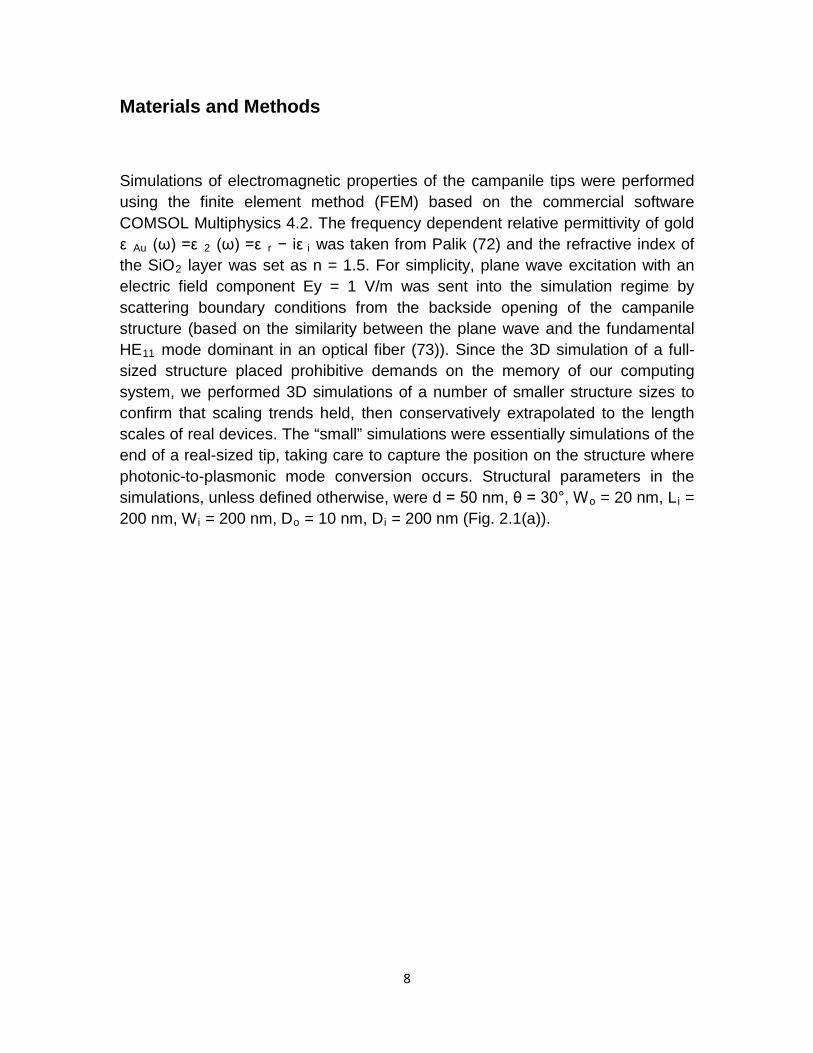
Simulations of electromagnetic properties of the campanile tips were performed using the finite element method (FEM) based on the commercial software COMSOL Multiphysics 4.2. The frequency dependent relative permittivity of gold ε Au (ω) =ε 2 (ω) =ε r − iε i was taken from Palik (72) and the refractive index of the SiO2 layer was set as n = 1.5. For simplicity, plane wave excitation with an electric field component Ey = 1 V/m was sent into the simulation regime by scattering boundary conditions from the backside opening of the campanile structure (based on the similarity between the plane wave and the fundamental HE11 mode dominant in an optical fiber (73)). Since the 3D simulation of a full-sized structure placed prohibitive demands on the memory of our computing system, we performed 3D simulations of a number of smaller structure sizes to confirm that scaling trends held, then conservatively extrapolated to the length scales of real devices. The “small” simulations were essentially simulations of the end of a real-sized tip, taking care to capture the position on the structure where photonic-to-plasmonic mode conversion occurs. Structural parameters in the simulations, unless defined otherwise, were d = 50 nm, θ = 30°, Wo = 20 nm, Li = 200 nm, Wi = 200 nm, Do = 10 nm, Di = 200 nm (Fig. 2.1(a)).
9
Results and Discussion
Perhaps still, the most common near-field imaging modality is the aperture-based NSOM, with the probes consisting of metal-coated tapered dielectric structures with a resolutiondefining sub-wavelength aperture at the apex (3, 51–57). While this geometry is ”background-free”, the boundary conditions for this type of optical waveguide demand that all propagating modes within the taper get cut off before reaching the aperture, causing only evanescent waves to leak out from the end, which results in low optical throughput and signal strength (1, 58). In addition, maximum probe input intensity is limited by thermal damage to the metal film in the taper region. Because throughput is inversely proportional to the fourth power of the aperture radius, signal-to-noise considerations in NSOM ultimately constrain aperture size, and resolution, to ~50 – 100 nm.
To get past the cut-off mode problem one can turn to a metal-insulator-metal (MIM) waveguide geometry (Fig. 2.1(a) inset). It is well-known that the symmetric SPP mode in a metal-insulator-metal (MIM) waveguide is supported without any cut-off frequency (59) no matter how thin the insulating layer. A linearly tapered MIM structure provides one of the simplest methods for overcoming the diffraction limit and has been utilized extensively at longer wavelengths, in the microwave (59) and terahertz regimes (60, 61). As the thickness D of the dielectric layer decreases, higher order modes are cut off, until only the fundamental plasmonic mode is allowed to propagate (the tapered MIM waveguide effectively acts as mode filter). In addition, the fundamental mode’s propagation constant increases as D decreases. Therefore, the SPP wavelength decreases as the structure is tapered down, analogous to the tapered adiabatic compression described previously (47, 62, 63). It has been demonstrated that efficient delivery of light to an ultra-small region is possible in 2D space using a tapered planar MIM structure (64–69), and in 3D space with an MIM dimple lens structure (70), which is similar to the campanile geometry. When a linearly tapered MIM structure with an optimal taper angle is employed, it is possible to convert ≥ 84% of the incident photonic mode energy into the fundamental SPP mode (67) (consistent with other geometries (71)), which then propagates and gets concentrated at the nanoscale end of the taper without ever being cut off (10).
10
Fig. 2.1. (a) 3D schematic of a campanile structure at the end of a gold-coated conical tapered NSOM fiber. A diagram of a metal-insulating-metal (MIM) structure is shown in the inset. (b) FEM simulations of a campanile structure with a final gap size Do = 10 nm and a round corner radius of 4 nm; λ = 713 nm was used here. The yz-section of the spatial profile of the steady state electric field amplitude near the end of the campanile, normalized to the amplitude of the incident field and a geometric factor (9). The white arrows indicate the polarization of the electric field. The simulation shows an 8% reduction in enhancement relative to the simulation in reference (9) with no rounding at the corners at the gap.
11
The concept of a robust 3D tapered structure forms the basis of the reproducible near-field campanile probes (Fig. 2.1(a)). The campanile geometry in this work consists of two symmetric linearly tapered Au cladding plates enclosing a SiO2 core. Using nanofabrication techniques like focused ion beam (FIB) milling, metal deposition and, potentially, dielectric material deposition), this design can easily be integrated at the apex of a number of scan probe types including atomic force microscope (AFM) cantilevers or tapered optical fibers like those used in conventional aperture-based NSOM (9). The campanile schematic shown in Fig. 2.1(a) is located at the end of a fiber probe, with a ~3-4 μm opening at the MIM backside designed to match the core region of a chemically-etched optical fiber taper. As with the dimple lens (70), the campanile design can take advantage of thin-film growth/deposition capabilities to effectively define a nanoscale gap size smaller than what is reproducibly achievable using other nanofabrication techniques. While the gap size Do and width Wo (see Fig. 2.1(a)) mainly determine the final spot size and field enhancement of the focusing point, the separation of the two metal plates Di will determine the efficiency of energy coupling from the photonic mode to the SPP mode, and the taper angle θ will determine the SPP transfer efficiency toward the end of the final aperture gap. For a linearly tapered two-dimensional (2D) MIM structure, the optimal taper angle is around 20°-40° (68), over which range the transfer efficiency shows only minor changes. For simplicity, we have used θ = 30° in our simulations.
Calculated electric field distributions and enhancements are shown in Fig. 2.1(b). The highly localized field near the gap has an enhancement comparable to that from a bowtie or dipolar optical antenna with the same sized gap (gap = 10 nm) (37). For comparison with other tip geometries given below, we use the convergent enhancement value at the gap center when appropriate (a few meshing layers away from the Au), where spurious unphysical field values from edge singularities in the simulation tend to be smoothed out. Simulations of structures with both sharp corners near the gap (9) and rounded corners (Fig.2. 1(b); 4 nm radii of curvature) were performed. The difference in the enhancement in those two cases is below 8%. Because of this modest difference, we use sharp corners in the following simulations of the campanile tip to reduce the simulation time. Also, the field polarization is aligned predominantly along the y axis near the gap, as expected. As mentioned above, conical adiabatically tapered (CAT) tips offer field localization capabilities over a broad spectral bandwidth, as well as extremely large field enhancements when operated in tip-(metal) substrate gap mode, with the potential for nearly-background free excitation. In order to directly compare the campanile probes with these geometries, we have run simulations
12
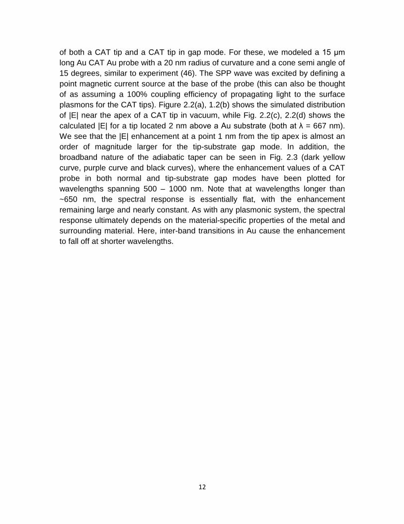
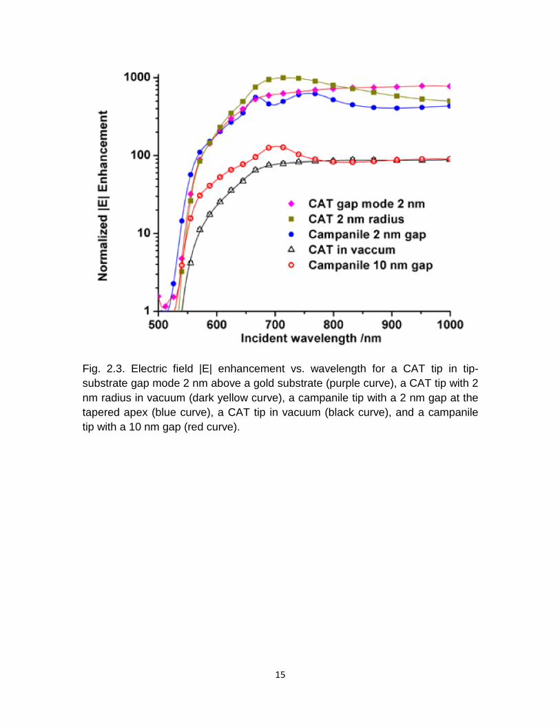
of both a CAT tip and a CAT tip in gap mode. For these, we modeled a 15 μm long Au CAT Au probe with a 20 nm radius of curvature and a cone semi angle of 15 degrees, similar to experiment (46). The SPP wave was excited by defining a point magnetic current source at the base of the probe (this can also be thought of as assuming a 100% coupling efficiency of propagating light to the surface plasmons for the CAT tips). Figure 2.2(a), 1.2(b) shows the simulated distribution of |E| near the apex of a CAT tip in vacuum, while Fig. 2.2(c), 2.2(d) shows the calculated |E| for a tip located 2 nm above a Au substrate (both at λ = 667 nm). We see that the |E| enhancement at a point 1 nm from the tip apex is almost an order of magnitude larger for the tip-substrate gap mode. In addition, the broadband nature of the adiabatic taper can be seen in Fig. 2.3 (dark yellow curve, purple curve and black curves), where the enhancement values of a CAT probe in both normal and tip-substrate gap modes have been plotted for wavelengths spanning 500 – 1000 nm. Note that at wavelengths longer than ~650 nm, the spectral response is essentially flat, with the enhancement remaining large and nearly constant. As with any plasmonic system, the spectral response ultimately depends on the material-specific properties of the metal and surrounding material. Here, inter-band transitions in Au cause the enhancement to fall off at shorter wavelengths.
13
Fig. 2.2. Cross-sections of the electric field distribution surrounding a CAT tip in vacuum are shown in (a-b). For the simulations, plasmonic current sources are placed directly in the tip shaft. The field distribution cross-sections for a CAT tip in tip-substrate gap mode are shown in (c-d). In this case, the fields in the gap mode are much larger and more localized (λ = 667 nm).
14
To assess the relative merits of the campanile geometry, we simulated campanile probes with a 2 nm gap and 10 nm gap, a 20 nm radius CAT probe with a 2 nm tip-substrate separation, as well as an ultrasharp 2 nm radius CAT probe in vaccum. We note that reproducible growth of a 2 nm-thick dielectric (or even thinner) is quite feasible with current growth/deposition techniques. On the other hand, the 2 nm radius-of-curvature metalized CAT probe may only exist in theoretical calculations because of metal material properties such as the stress-limited finite grain size of noble plasmonic metals. Furthermore, maintaining an ultrasharp tip on a soft plasmonic metal probe during scanning can be problematic in real experiments. The results of this simulation are plotted in Fig. 2.3 (blue curve), where it is shown that the smallest physical feature of the probe structure (e.g. the gap size or the tip radius) predominantly determines the final optical confinement and enhancement of all the adiabatic compression probes (74). Note that the campanile tip provides nearly the same enhancement, ultralocalized field concentration (i.e. – high spatial resolution for imaging and spectroscopy), and broadband response, but without operating in tip-substrate gap mode. In other words, by effectively putting the gap on the tip while still utilizing plasmonic adiabatic compression, the campanile probes significantly increase the general applicability of nano-optical investigations (e.g. – samples with thickness greater than~2nm can now be studied) without sacrificing the benefits associated with the more-limited tip-substrate gap modality. As with all near-field probes, the campanile tips also have the benefit of probing only surface/interface material located within a few nm of the tip, eliminating most background spectroscopic signal not arising from the interface region of interest (i.e. – there is very little excitation of signal from the “bulk”, or from the surrounding solution if the tip is immersed in liquid (75). Also, the electric field polarization for the campanile probe is in the plane of the sample, which is complementary to the CAT tip polarization that is primarily oriented normal to the surface.
15
Fig. 2.3. Electric field |E| enhancement vs. wavelength for a CAT tip in tip-substrate gap mode 2 nm above a gold substrate (purple curve), a CAT tip with 2 nm radius in vacuum (dark yellow curve), a campanile tip with a 2 nm gap at the tapered apex (blue curve), a CAT tip in vacuum (black curve), and a campanile tip with a 10 nm gap (red curve).
16
Also, visible in Fig. 2.3 are a couple of small oscillations in the enhancement spectrum of the campanile tip in the 650 – 800 nm region. These “wiggles” in the spectrum result from weak geometric resonances in the design. As with the CAT tip, enhancement falls off at shorter wavelengths due to interband transitions in the Au. Though not discussed here, we expect the large enhancements to extend well into the infrared (IR) region based on Au material properties (and suitable choice of dielectric material). Metals other than Au (e.g. Ag or Al) can be used for extending the enhancement into the blue, or even ultraviolet (UV), region of the visible spectrum. For demanding applications such as heat-assisted magnetic recording that require a particularly robust field-concentrating structure, transparent conducting oxides can be used as the plasmonic material if operating near the visible is not required (76). As mentioned above, completely background-free near-field excitation is a clear goal for nano-optical imaging and spectroscopy. While an ideal adiabatic taper will concentrate and guide the SPP mode toward the campanile apex without scattering light out, in practice it is likely that some radiation will scatter from the edges (and edge roughness) of the taper and onto the sample before reaching the tip end. In addition, a small fraction of the photonic mode that is not converted fully to the SPP mode by the campanile probe will also partially leak out from the Au-uncovered sides. For these reasons, we refer to the campanile tips as being ”nearly-background-free” rather than strictly “background free”, though based on simulations and preliminary experiments, we expect the intensity of this excess scattered light on the sample to be very small relative to the ultra-enhanced fields at the apex. When considering that one will often operate in a mode where signal is collected back through the gap of the campanile tip, the total collected background from the sample arising from the edge-scattered light is expected to be insignificant, and so far has been below the noise floor in our experiments (9). More extensive simulations (and hyperspectral imaging experiments) investigating this potential source of background are currently under way.
With regard to roughness, another potential advantage of the campanile geometry over the CAT tip is that it is less susceptible to surface roughness at the metal-dielectric interfaces of the waveguides, and thus to losses and other effects related to surface roughness along the tapered waveguide. This is because the optically-relevant surfaces of the campanile tip are formed by depositing the metal on a smooth dielectric, while the waveguiding metal-air surface of the CAT tips are often formed by evaporation or etching techniques (though advances based on template stripping have recently been demonstrated) (77).
17
In cylindrical coordinates, the equivalent of the MIM waveguide is a coaxial waveguide, which also supports a fundamental mode that propagates without cut-off no matter how thin the dielectric layer (see (41) and references therein). Therefore, a tapered coaxial waveguide will also have the benefits of the campanile tip when excited with radially polarized light. In this case, the localized, enhanced spot will be z-polarized and its size will be determined by the radius of curvature of the apex of the central pin. In passing, we note that it may be tempting to design a campanile-type tip with metal layers on all four sides of campanile structure in order to create a polarization-insensitive structure, as in the case of cross optical antennas (78–80). However, even with the four sides of the waveguide being electrically isolated from one another, all modes supported by this geometry will be cut off when the thickness of the dielectric is tapered below a certain value; i.e. – it behaves very similarly to a conventional aperture-based NSOM probe.
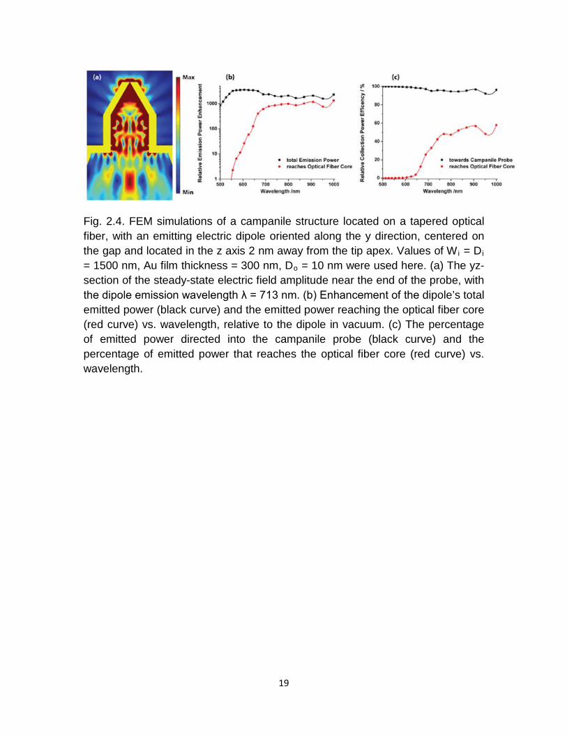
Besides efficiently concentrating light to nanoscale dimensions, reciprocity would imply that the campanile probe also efficiently collects emission (81), and simulations show that this is indeed the case. To understand this, we simulated a larger scale campanile structure probe with an electric dipole located near the middle of the nano-gap (Fig. 2.4). The dipole was positioned 2 nm away from the campanile apex in the z direction and oscillated along the y direction. In this simulation, the campanile structure sits near the end of a tapered optical fiber (20 degree taper; Nufern 780-HP fiber ncore = 1.4597, ncladding = 1.4535), which has a 4.4 μm core size. The backside aperture of the campanile structure is 1.5 μm by 1.5 μm in size (Fig. 2.4) and is located at a position on the fiber where the fiber taper reaches a diameter of 3 μm. Both the total emitted power from the dipole and the power in the fiber at the position where the tapered optical fiber reaches its full core size were calculated. The latter represents an estimate of how efficiently the SPPs in the campanile back-couple to the photonic mode in the optical fiber. Figure 2.4(b) shows that the total power emitted by the dipole is largely enhanced (more than 1000 times) compared with the same dipole in vacuum. These numbers are similar for a CAT probes either in tip-substrate gap mode or with ultrasharp (~2 nm) tip radii. In addition, more than 90% of that total emitted power is directed into the campanile MIM waveguide (Fig. 2.4(a), 2.4(c)). This efficient emission collection can be attributed to the large optical density of states at the campanile probe apex and the enhanced spontaneous emission near the Au cavity. Also notable is that > 50% of the power reaches the fiber core

18
in the campanile probe (Fig. 2.4(a), 2.4(c)), with metal losses and radiation accounting for the bulk of the lost power.
19
Fig. 2.4. FEM simulations of a campanile structure located on a tapered optical fiber, with an emitting electric dipole oriented along the y direction, centered on the gap and located in the z axis 2 nm away from the tip apex. Values of Wi = Di = 1500 nm, Au film thickness = 300 nm, Do = 10 nm were used here. (a) The yz-section of the steady-state electric field amplitude near the end of the probe, with the dipole emission wavelength λ = 713 nm. (b) Enhancement of the dipole’s total emitted power (black curve) and the emitted power reaching the optical fiber core (red curve) vs. wavelength, relative to the dipole in vacuum. (c) The percentage of emitted power directed into the campanile probe (black curve) and the percentage of emitted power that reaches the optical fiber core (red curve) vs. wavelength.
20
Conclusion
Finally, we emphasize the breadth of optical characterization techniques that are possible at the nanoscale using optical transformer-type probes such as the campanile tip, which combines wide bandwidth with maximum field enhancement and resolution. This tip geometry provides near-optimal excitation and collection properties for nano-Raman and nano-IR/FTIR hyperspectral imaging and also enables measurements such as white-light nano-ellipsometry/interferometric mapping of dielectric functions, nonlinear optical experiments that involve multiple optical frequencies (such as sum-frequency and second harmonic generation), coherent anti-Stokes and stimulated Raman spectroscopy, as well as other ultrafast pump-probe investigations of local dynamics (82).
In conclusion, we have compared the “campanile” probe paradigm with other nano-optical probe geometries. This type of hybrid photonic-plasmonic structure geometry effectively marries the beneficial properties of photonic waveguides, plasmonic waveguides, and optical antennas. We used FEM to simulate conventional aperture-based probes, traditional a-NSOM tips and the state-of-the-art adiabatic-compression-type probes, examining their nano-optical properties relative to those of the campanile structure. More specifically, beyond insights from the circuit theory of metal-optics (11), understanding of the relative strengths and weaknesses of each NSOM probe geometry served as the guideline for the design of the campanile tips, resulting in their superior field coupling, spectral bandwidth, enhancement, and resolution capabilities. We expect these types of probes to have a broad impact as they enable a general approach towards manipulating light and the investigating light-matter interactions at the nanoscale.
21
Reference
1. H. A. Bethe, Theory of diffraction by small holes. Phys Rev 66, 163-182 (1944).
2. E. A. Ash, G. Nicholls, Super-Resolution Aperture Scanning Microscope. Nature 237, 510-& (1972).
3. M. A. Paesler, P. J. Moyer, Near-Field Optics: Theory, Instrumentation and Applications. (Wiley, New York, 1996).
4. D. W. Pohl, W. Denk, M. Lanz, Optical Stethoscopy - Image Recording with Resolution Lambda/20. Applied Physics Letters 44, 651-653 (1984).
5. E. Betzig, J. K. Trautman, Near-Field Optics: Microscopy, Spectroscopy, and Surface Modification Beyond the Diffraction Limit. Science 257, 189-195 (1992).
6. S. Kawata, Y. Inouye, P. Verma, Plasmonics for near-field nano-imaging and superlensing. Nat Photonics 3, 388-394 (2009).
7. L. Novotny, B. Hecht, Principles of Nano-Optics. (Cambridge University Press, 2006).
8. A. V. Zayats, D. Richards, Eds., Nano-optics and Near-field Optical Microscopy, (Artech House, 2008).
9. W. Bao et al., Mapping local charge recombination heterogeneity by multidimensional nanospectroscopic imaging. Science 338, 1317-1321 (2012).
10. H. Choo et al., Nanofocusing in a metal-insulator-metal gap plasmon waveguide with a three-dimensional linear taper. Nat Photon 6, 838-844 (2012).
11. M. Staffaroni, J. Conway, S. Vedantam, J. Tang, E. Yablonovitch, Circuit analysis in metal-optics. Photonics and Nanostructures - Fundamentals and Applications 10, 166-176 (2012).
12. J. Wessel, SURFACE-ENHANCED OPTICAL MICROSCOPY. J. Opt. Soc. Am. B-Opt. Phys. 2, 1538-1541 (1985).
13. Y. Inouye, S. Kawata, NEAR-FIELD SCANNING OPTICAL MICROSCOPE WITH A METALLIC PROBE TIP. Opt. Lett. 19, 159-161 (1994).
14. F. Zenhausern, Y. Martin, H. K. Wickramasinghe, SCANNING INTERFEROMETRIC APERTURELESS MICROSCOPY - OPTICAL IMAGING AT 10 ANGSTROM RESOLUTION. Science 269, 1083-1085 (1995).
15. L. Novotny, S. J. Stranick, Near-field optical microscopy and spectroscopy with pointed probes. Annual Review of Physical Chemistry 57, 303-331 (2006).
22
16. N. Anderson, A. Bouhelier, L. Novotny, Near-field photonics: tip-enhanced microscopy and spectroscopy on the nanoscale. Journal of Optics A: Pure and Applied Optics 8, S227-S233 (2006).
17. R. Hillenbrand, F. Keilmann, Complex optical constants on a subwavelength scale. Physical Review Letters 85, 3029-3032 (2000).
18. J. Stadler, T. Schmid, R. Zenobi, Developments in and practical guidelines for tip-enhanced Raman spectroscopy. Nanoscale 4, 1856-1870 (2012).
19. D. Roy, J. Wang, C. Williams, Novel methodology for estimating the enhancement factor for tip-enhanced Raman spectroscopy. Journal of Applied Physics 105, 013530 (2009).
20. K. F. Domke, B. Pettinger, Studying Surface Chemistry beyond the Diffraction Limit: 10 Years of TERS. ChemPhysChem 11, 1365-1373 (2010).
21. K. G. Lee et al., Vector field microscopic imaging of light. Nat Photonics 1, 53-56 (2007).
22. D. S. Kim et al., Real-Space Mapping of the Strongly Coupled Plasmons of Nanoparticle Dimers. Nano Letters 9, 3619-3625 (2009).
23. R. L. Olmon et al., Determination of Electric-Field, Magnetic-Field, and Electric-Current Distributions of Infrared Optical Antennas: A Near-Field Optical Vector Network Analyzer. Physical Review Letters 105, 167403 (2010).
24. A. Hartschuh, Tip-Enhanced Near-Field Optical Microscopy. Angewandte Chemie-International Edition 47, 8178-8191 (2008).
25. J. Stadler, T. Schmid, R. Zenobi, Nanoscale Chemical Imaging Using Top-Illumination Tip-Enhanced Raman Spectroscopy. Nano Letters 10, 4514-4520 (2010).
26. S. M. Nie, S. R. Emery, Probing single molecules and single nanoparticles by surface-enhanced Raman scattering. Science 275, 1102-1106 (1997).
27. A. Jamshidi et al., NanoPen: Dynamic, Low-Power, and Light-Actuated Patterning of Nanoparticles. Nano Letters 9, 2921-2925 (2009).
28. A. T. Zayak et al., Chemical Raman Enhancement of Organic Adsorbates on Metal Surfaces. Physical Review Letters 106, 083003 (2011).
29. C. F. Bohren, D. R. Huffman, in Absorption and Scattering of Light by Small Particles. (Wiley-VCH Verlag GmbH, 2007), pp. 499-519.
30. Y. Saito, T. Murakami, Y. Inouye, S. Kawata, Fabrication of silver probes for localized plasmon excitation in near-field Raman spectroscopy. Chem Lett 34, 920-921 (2005).
31. B. Pettinger, B. Ren, G. Picardi, R. Schuster, G. Ertl, Nanoscale probing of adsorbed species by tip-enhanced Raman spectroscopy. Physical Review Letters 92, - (2004).
23
32. C. C. Neacsu, J. Dreyer, N. Behr, M. B. Raschke, Scanning-probe Raman spectroscopy with single-molecule sensitivity. Physical Review B (Condensed Matter and Materials Physics) 73, 193406-193404 (2006).
33. M. Sackrow, C. Stanciu, M. A. Lieb, A. J. Meixner, Imaging nanometre-sized hot spots on smooth Au films with high-resolution tip-enhanced luminescence and Raman near-field optical microscopy. ChemPhysChem 9, 316-320 (2008).
34. T. Deckert-Gaudig, V. Deckert, Ultraflat Transparent Gold Nanoplates - Ideal Substrates for Tip-enhanced Raman Scattering Experiments. Small 5, 432-436 (2009).
35. K. F. Domke, B. Pettinger, In Situ Discrimination between Axially Complexed and Ligand-Free Co Porphyrin on Au(111) with Tip-Enhanced Raman Spectroscopy. ChemPhysChem 10, 1794-1798 (2009).
36. R. Esteban, R. Vogelgesang, K. Kern, Tip-substrate interaction in optical near-field microscopy. Physical Review B 75, 195410 (2007).
37. P. Biagioni, J. S. Huang, B. Hecht, Nanoantennas for visible and infrared radiation. Rep. Prog. Phys. 75, 024402 (2012).
38. P. Muhlschlegel, H. J. Eisler, O. J. F. Martin, B. Hecht, D. W. Pohl, Resonant Optical Antennas. Science 308, 1607-1609 (2005).
39. P. J. Schuck, D. P. Fromm, A. Sundaramurthy, G. S. Kino, W. E. Moerner, Improving the mismatch between light and nanoscale objects with gold bowtie nanoantennas. Physical Review Letters 94, 017402 (2005).
40. J. N. Farahani, D. W. Pohl, H. J. Eisler, B. Hecht, Single quantum dot coupled to a scanning optical antenna: A tunable superemitter. Physical Review Letters 95, 017402 (2005).
41. A. Weber-Bargioni et al., Hyperspectral Nanoscale Imaging on Dielectric Substrates with Coaxial Optical Antenna Scan Probes. Nano Letters 11, 1201-1207 (2011).
42. L. Neumann et al., Extraordinary Optical Transmission Brightens Near-Field Fiber Probe. Nano Letters 11, 355-360 (2011).
43. Y. Wang, W. Srituravanich, C. Sun, X. Zhang, Plasmonic nearfield scanning probe with high transmission. Nano Letters 8, 3041-3045 (2008).
44. L. Wang, S. M. Uppuluri, E. X. Jin, X. F. Xu, Nanolithography using high transmission nanoscale bowtie apertures. Nano Letters 6, 361-364 (2006).
45. J. A. Matteo et al., Spectral analysis of strongly enhanced visible light transmission through single C-shaped nanoapertures. Applied Physics Letters 85, 648-650 (2004).
46. C. Ropers et al., Grating-coupling of surface plasmons onto metallic tips: A nanoconfined light source. Nano Letters 7, 2784-2788 (2007).
24
47. C. C. Neacsu et al., Near-Field Localization in Plasmonic Superfocusing: A Nanoemitter on a Tip. Nano Letters 10, 592-596 (2010).
48. D. Sadiq et al., Adiabatic Nanofocusing Scattering-Type Optical Nanoscopy of Individual Gold Nanoparticles. Nano Letters 11, 1609-1613 (2011).
49. F. De Angelis et al., Nanoscale chemical mapping using three-dimensional adiabatic compression of surface plasmon polaritons. Nature Nanotechnology 5, 67-72 (2010).
50. S. Berweger, J. M. Atkin, R. L. Olmon, M. B. Raschke, Light on the Tip of a Needle: Plasmonic Nanofocusing for Spectroscopy on the Nanoscale. J Phys Chem Lett 3, 945-952 (2012).
51. E. Verhagen, M. Spasenovic, A. Polman, L. Kuipers, Nanowire Plasmon Excitation by Adiabatic Mode Transformation. Physical Review Letters 102, 203904 (2009).
52. Y. D. Suh, R. Zenobi, Improved probes for scanning near-field optical microscopy. Advanced Materials 12, 1139 (2000).
53. S. Sun, G. J. Leggett, Matching the resolution of electron beam lithography by scanning near-field photolithography. Nano Letters 4, 1381-1384 (2004).
54. T. H. Taminiau, R. J. Moerland, F. B. Segerink, L. Kuipers, N. F. van Hulst, lambda/4 Resonance of an optical monopole antenna probed by single molecule fluorescence. Nano Letters 7, 28-33 (2007).
55. J.-S. Bouillard, S. Vilain, W. Dickson, A. V. Zayats, Hyperspectral imaging with scanning near-field optical microscopy: applications in plasmonics. Optics Express 18, 16513-16519 (2010).
56. M. Burresi et al., Probing the Magnetic Field of Light at Optical Frequencies. Science 326, 550-553 (2009).
57. H. W. Kihm et al., Bethe-hole polarization analyser for the magnetic vector of light. Nature Communications 2, 451 (2011).
58. L. Novotny, C. Hafner, Light-Propagation in a Cylindrical Wave-Guide with a Complex, Metallic, Dielectric Function. Physical Review E 50, 4094-4106 (1994).
59. D. M. Pozar, Microwave engineering. (J. Wiley, Hoboken, NJ, ed. 3rd, 2005), pp. xvii, 700 p.
60. E. Peytavit, J. F. Lampin, T. Akalin, L. Desplanque, Integrated terahertz TEM horn antenna. Electron. Lett. 43, 73-75 (2007).
61. D. Dragoman, M. Dragoman, Terahertz fields and applications. Progress in Quantum Electronics 28, 1-66 (2004).
25
62. A. J. Babadjanyan, N. L. Margaryan, K. V. Nerkararyan, Superfocusing of surface polaritons in the conical structure. Journal of Applied Physics 87, 3785-3788 (2000).
63. M. I. Stockman, Nanofocusing of optical energy in tapered plasmonic waveguides. Physical Review Letters 93, - (2004).
64. D. F. P. Pile, D. K. Gramotnev, Adiabatic and nonadiabatic nanofocusing of plasmons by tapered gap plasmon waveguides. Applied Physics Letters 89, 041111 (2006).
65. H. Choi, D. F. P. Pile, S. Nam, G. Bartal, X. Zhang, Compressing surface plasmons for nano-scale optical focusing. Optics Express 17, 7519-7524 (2009).
66. M. Schnell et al., Nanofocusing of mid-infrared energy with tapered transmission lines. Nat Photonics 5, 283-287 (2011).
67. P. Ginzburg, D. Arbel, M. Orenstein, Gap plasmon polariton structure for very efficient microscale-to-nanoscale interfacing. Opt. Lett. 31, 3288-3290 (2006).
68. J. Conway, 3251514, University of California, Los Angeles, United States -- California (2006).
69. D. K. Gramotnev, D. F. P. Pile, M. W. Vogel, X. Zhang, Local electric field enhancement during nanofocusing of plasmons by a tapered gap. Physical Review B 75, - (2007).
70. S. Vedantam et al., A Plasmonic Dimple Lens for Nanoscale Focusing of Light. Nano Letters 9, 3447-3452 (2009).
71. X. W. Chen, V. Sandoghdar, M. Agio, Highly Efficient Interfacing of Guided Plasmons and Photons in Nanowires. Nano Letters 9, 3756-3761 (2009).
72. E. D. Palik, G. Ghosh, Knovel (Firm). (Academic Press, San Diego, 1998). 73. K. Okamoto, Fundamentals of optical waveguides. Optics and photonics
(Academic, San Diego, Calif. ; London, 2000), pp. xiv, 428 p. 74. W. H. Zhang, X. D. Cui, O. J. F. Martin, Local field enhancement of an
infinite conical metal tip illuminated by a focused beam. J Raman Spectrosc 40, 1338-1342 (2009).
75. T. Schmid, B. S. Yeo, G. Leong, J. Stadler, R. Zenobi, Performing tip-enhanced Raman spectroscopy in liquids. J Raman Spectrosc 40, 1392-1399 (2009).
76. G. V. Naik, J. Kim, A. Boltasseva, Oxides and nitrides as alternative plasmonic materials in the optical range (Invited). Opt. Mater. Express 1, 1090-1099 (2011).
26
77. T. W. Johnson et al., Highly Reproducible Near-Field Optical Imaging with Sub-20-nm Resolution Based on Template-Stripped Gold Pyramids. Acs Nano 6, 9168-9174 (2012).
78. P. Biagioni, J. S. Huang, L. Duo, M. Finazzi, B. Hecht, Cross Resonant Optical Antenna. Physical Review Letters 102, 256801 (2009).
79. Z. Zhang et al., Manipulating Nanoscale Light Fields with the Asymmetric Bowtie Nano-Colorsorter. Nano Letters 9, 4505-4509 (2009).
80. A. McLeod et al., Nonperturbative Visualization of Nanoscale Plasmonic Field Distributions via Photon Localization Microscopy. Physical Review Letters 106, 037402 (2011).
81. H. Eghlidi, K. G. Lee, X. W. Chen, S. Gotzinger, V. Sandoghdar, Resolution and Enhancement in Nanoantenna-Based Fluorescence Microscopy. Nano Letters 9, 4007-4011 (2009).
82. P. Vasa, C. Ropers, R. Pomraenke, C. Lienau, Ultra-fast nano-optics. Laser Photon. Rev. 3, 483-507 (2009).
27
Chapter 3 : Mapping InP nanowires local charge recombination heterogeneity
Most of the work described in this chapter was published in
Science 338 (6112), 1317-1321, 2012
Introduction and Motivation
An ongoing challenge to understanding matter at the nanoscale is the difficulty in carrying out local optical spectroscopy. On a fundamental level, this should be possible by squeezing light beyond the diffraction limit (1-4). Optical-antenna-based geometries have been designed to address this ‘nanospectroscopy imaging’ problem by transforming light from the far-field to the near-field, but unfortunately with serious limitations on sensitivity, bandwidth, resolution, and/or sample types (5).
Herein we report a strategy for overcoming these limitations by designing a unique geometry capable of efficiently coupling far-field light to the near-field and vice-versa without excess background illumination, and more significantly, doing so over a wide range of wavelengths. The geometry consists of a three-dimensional tapered structure terminating in a nano-gap (Fig. 3.1A), thus giving a shape resembling that of a “campanile” bell tower (hereafter referred to as campanile). We demonstrate how the campanile allowed us to achieve hyperspectral nanoimaging of local optoelectonic properties in InP nanowires by exciting and collecting signal through the tips. InP nanowires, with their direct solar-spectrum-matched bandgap and assumed low surface recombination velocity, are expected to be the central functional elements of many next generation light-harvesting devices. By using the campanile, we gain access to a new level of information, wherein a full spectrum is collected at each pixel in the scan (often referred to as hyperspectral or multidimensional imaging). Specifically, we reveal photoluminescence (PL) heterogeneity along individual nanowires, in effect mapping local charge recombination originating from trap states – critical optoelectronic information unobtainable using previous methods. This work shows that the solution to the nanospectroscopy imaging problem offered by the campanile constitutes a new paradigm in plasmonics, non-linear optics, and especially near-field investigations.
28
This new concept does not require the trade-offs made in the past that limited performance. Previous near-field probe geometries, for example, have been engineered with extraordinary optical transmission (6) or coupled optical antenna structures (7, 8) directly on the scan-probe apex, greatly improving coupling efficiencies. However, these rely on resonant structures with limited spectral bandwidth and have often used excitation modalities that are not background-free (9, 10). Of note are recent approaches combining elements of apertureless near-field scanning microscopy (a-NSOM) tips with efficient photon-to-plasmon coupling structures that can be illuminated far from the sample (10, 11). When designed correctly, these types of probes can be broadband since they exploit adiabatic plasmonic compression (12, 13). There is, however, one primary drawback to these probes: maximum enhancement is only achieved in the tip-substrate gap mode. The tip-substrate gap mode can yield large near-field signals, but requires both a metallic substrate and a very small tip-substrate gap. Therefore, only very thin samples (e.g. molecular monolayers) can be studied. This work overcomes all these problems, offering a different concept that unites broadband field enhancement and confinement with efficient bi-directional coupling between far-field and near-field electromagnetic energy, thereby enabling the translation of the wide spectrum of optical measurement modalities to the nm scale. Here, we take advantage of the campanile concept to map optoelectronic properties of InP NWs.
The campanile probe is based on a 3D tapered metal-insulator-metal (MIM) structure ending in a nanogap (Fig. 3.1A-C). Our simulations show that this geometry provides efficient coupling between the far- and near-fields (Fig. 3.1D) since the fundamental mode in an MIM structure is supported without any cut-off frequency no matter how thin the insulating layer (12). In the optical regime, where plasmonic effects become important at small length scales, it has been shown that efficient delivery of far-field light to an ultra-small region is possible in two dimensions using a tapered planar MIM structure (> 84% conversion efficiency (14)), and in three dimensions with a dimple lens structure (15). Equally important is the fact that the campanile probe’s bi-directional coupling is efficient over a large bandwidth (Fig. 3.1G), taking advantage of an adiabatically-tapered (12, 13) geometry utilized at longer wavelengths (e.g., the microwave and terahertz regimes (16)) to provide one of the simplest broadband methods for effectively overcoming the diffraction limit. The bandwidth is limited only by metal absorption at short wavelengths, and in principle can be extended well into the infrared region (and beyond). Other metals can be used for expanding enhancements into the blue or ultraviolet (UV) regions.
The plasmonic mode in the campanile is adiabatically squeezed into the nanogap region. Therefore, as shown in Fig. 3.1E-F, the size of the campanile gap
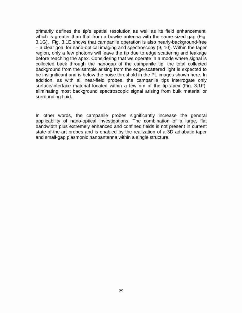
29
primarily defines the tip’s spatial resolution as well as its field enhancement, which is greater than that from a bowtie antenna with the same sized gap (Fig. 3.1G). Fig. 3.1E shows that campanile operation is also nearly-background-free – a clear goal for nano-optical imaging and spectroscopy (9, 10). Within the taper region, only a few photons will leave the tip due to edge scattering and leakage before reaching the apex. Considering that we operate in a mode where signal is collected back through the nanogap of the campanile tip, the total collected background from the sample arising from the edge-scattered light is expected to be insignificant and is below the noise threshold in the PL images shown here. In addition, as with all near-field probes, the campanile tips interrogate only surface/interface material located within a few nm of the tip apex (Fig. 3.1F), eliminating most background spectroscopic signal arising from bulk material or surrounding fluid.
In other words, the campanile probes significantly increase the general applicability of nano-optical investigations. The combination of a large, flat bandwidth plus extremely enhanced and confined fields is not present in current state-of-the-art probes and is enabled by the realization of a 3D adiabatic taper and small-gap plasmonic nanoantenna within a single structure.
30
Fig. 3.1 Structure and optical properties of the 3D tapered (campanile) far-field to near-field transformer. The campanile geometry (A) is composed of a tapered metal insulator–metal waveguide fabricated at the end of a tapered glass fiber (B) by focused ion beam milling. Its shape resembles that of a bell tower of the same name (inset: photo of the Berkeley campanile), with a 39 nm (±2 nm) gap between the 3D tapered Au plates (C). (D) Finite element simulations reveal the highly efficient bidirectional coupling between macro and nano length scales (the electric field strength color-scale contrast is saturated to show the much weaker

31
photonic and weakly confined plasmonic modes). Extending the contrast over the full color scale shows the nearly background-free near-field enhancement at the tip apex (E), while maintaining the linear polarization of the far field (F) (gap size = 10 nm; wavelength = 666 nm). (G) The ultralarge field (|E|) enhancement for a campanile with a 2 nm gap extends over larger bandwidth (red curve) than does a coupled optical bowtie antenna (blue curve) with a 2 nm gap or a sharp Au tip with a 20 nm radius of curvature (gray curve; assuming 100% light-coupling efficiency to the Au tip).
32
Results and Discussions
Using now-standard nanofabrication techniques, the design illustrated in Fig. 3.1A can easily be integrated at the apex of a number of scan probes including atomic force microscope (AFM) cantilevers or tapered optical fibers such as those used in conventional aperture-based NSOM. Representative images of a campanile tip and a gap used in this work are shown in Fig. 3.1B and C. For a linearly tapered 3D MIM structure, the optimal taper angle is around 20o-40o, over which range the transfer efficiency shows only minor changes (12). We point out that similar properties could be obtained in a tapered cylindrical coaxial structure.
To demonstrate the utility of this concept, campanile tips with ~ 40 nm-wide apertures were used to map out the inhomogeneous radiative recombination in individual indium phosphide (InP) nanowires (NWs). InP NWs were chosen based on their interesting PL emission properties and their potential as an ideal nanomaterial for light harvesting due to the 1.4 eV bandgap and assumed low surface recombination rates (17-19). Trap states are believed to be responsible for many optical phenomena in nanocrystals and wires (20, 21) including surface-state-mediated luminescence modification in InP NWs (22), but are not well-understood due to optical resolution limitations. Gaining this crucial insight requires both local optical excitation and local luminescence collection, which is provided by the campanile tip.
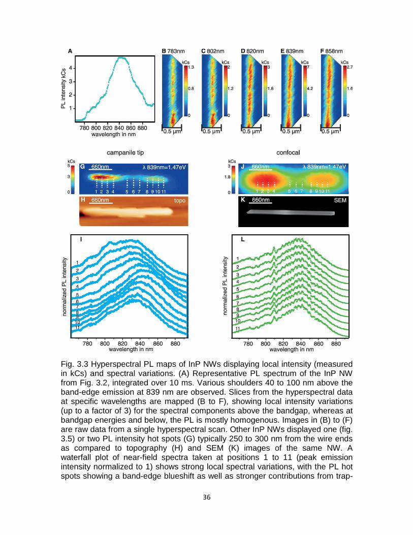
The glass fiber with the campanile tip was mounted in a shear-force scanner and coupled to a laser (633 nm). The ~ zeptoliter near-field spot was scanned over the sample to locally excite the InP NWs and to collect the PL. Because of the campanile’s broadband enhancement, only 100 µW of pre-fiber-coupled excitation power (< 1/10th of a basic laser pointer) was needed to collect and disperse a full spectrum using a high resolution grating set to observe emission between 760 and 900 nm. With just 10 ms integration time, a signal-to-noise ratio > 60/1 was achieved (Fig. 3.3A).
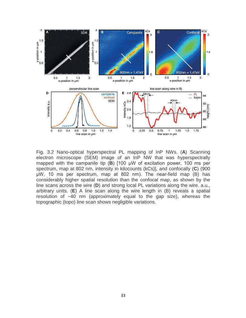
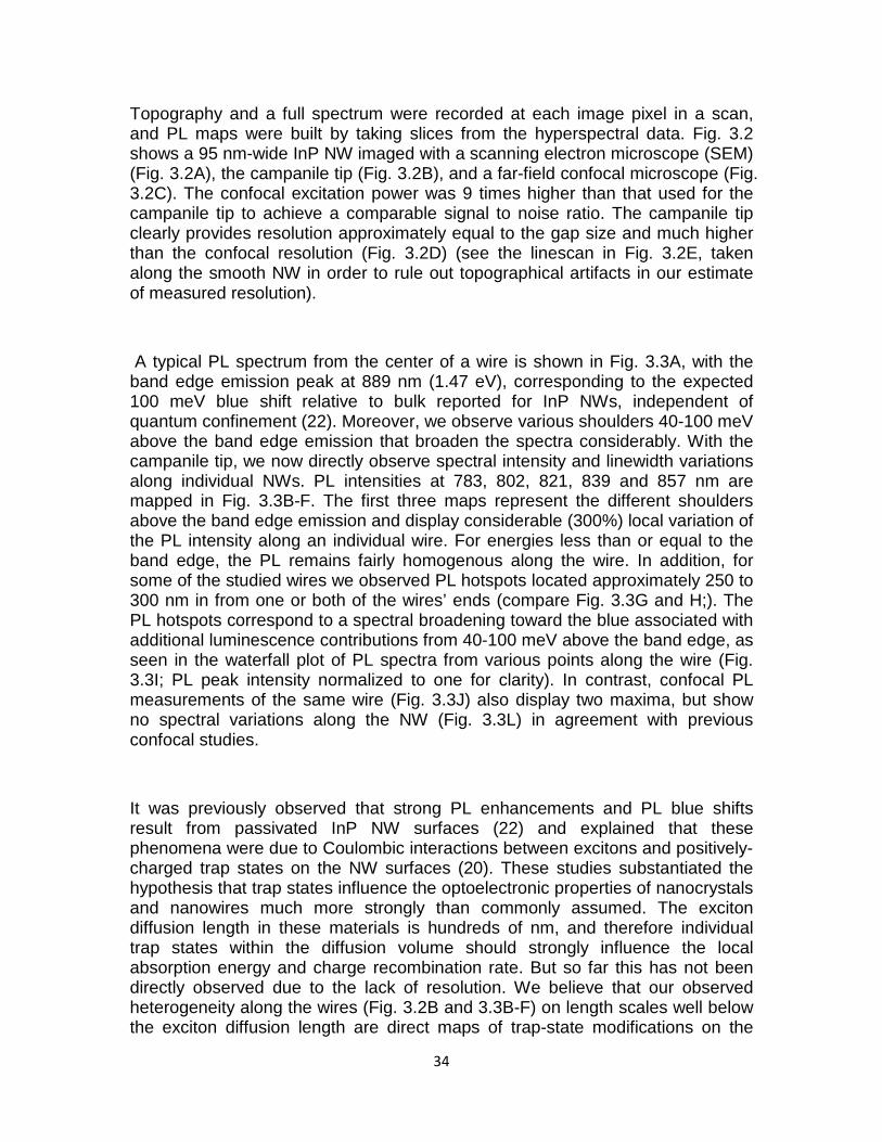
33
Fig. 3.2 Nano-optical hyperspectral PL mapping of InP NWs. (A) Scanning electron microscope (SEM) image of an InP NW that was hyperspectrally mapped with the campanile tip (B) [100 μW of excitation power, 100 ms per spectrum, map at 802 nm, intensity in kilocounts (kCs)], and confocally (C) (900 μW, 10 ms per spectrum, map at 802 nm). The near-field map (B) has considerably higher spatial resolution than the confocal map, as shown by the line scans across the wire (D) and strong local PL variations along the wire. a.u., arbitrary units. (E) A line scan along the wire length in (B) reveals a spatial resolution of ~40 nm (approximately equal to the gap size), whereas the topographic (topo) line scan shows negligible variations.
34
Topography and a full spectrum were recorded at each image pixel in a scan, and PL maps were built by taking slices from the hyperspectral data. Fig. 3.2 shows a 95 nm-wide InP NW imaged with a scanning electron microscope (SEM) (Fig. 3.2A), the campanile tip (Fig. 3.2B), and a far-field confocal microscope (Fig. 3.2C). The confocal excitation power was 9 times higher than that used for the campanile tip to achieve a comparable signal to noise ratio. The campanile tip clearly provides resolution approximately equal to the gap size and much higher than the confocal resolution (Fig. 3.2D) (see the linescan in Fig. 3.2E, taken along the smooth NW in order to rule out topographical artifacts in our estimate of measured resolution).
A typical PL spectrum from the center of a wire is shown in Fig. 3.3A, with the band edge emission peak at 889 nm (1.47 eV), corresponding to the expected 100 meV blue shift relative to bulk reported for InP NWs, independent of quantum confinement (22). Moreover, we observe various shoulders 40-100 meV above the band edge emission that broaden the spectra considerably. With the campanile tip, we now directly observe spectral intensity and linewidth variations along individual NWs. PL intensities at 783, 802, 821, 839 and 857 nm are mapped in Fig. 3.3B-F. The first three maps represent the different shoulders above the band edge emission and display considerable (300%) local variation of the PL intensity along an individual wire. For energies less than or equal to the band edge, the PL remains fairly homogenous along the wire. In addition, for some of the studied wires we observed PL hotspots located approximately 250 to 300 nm in from one or both of the wires’ ends (compare Fig. 3.3G and H;). The PL hotspots correspond to a spectral broadening toward the blue associated with additional luminescence contributions from 40-100 meV above the band edge, as seen in the waterfall plot of PL spectra from various points along the wire (Fig. 3.3I; PL peak intensity normalized to one for clarity). In contrast, confocal PL measurements of the same wire (Fig. 3.3J) also display two maxima, but show no spectral variations along the NW (Fig. 3.3L) in agreement with previous confocal studies.
It was previously observed that strong PL enhancements and PL blue shifts result from passivated InP NW surfaces (22) and explained that these phenomena were due to Coulombic interactions between excitons and positively-charged trap states on the NW surfaces (20). These studies substantiated the hypothesis that trap states influence the optoelectronic properties of nanocrystals and nanowires much more strongly than commonly assumed. The exciton diffusion length in these materials is hundreds of nm, and therefore individual trap states within the diffusion volume should strongly influence the local absorption energy and charge recombination rate. But so far this has not been directly observed due to the lack of resolution. We believe that our observed heterogeneity along the wires (Fig. 3.2B and 3.3B-F) on length scales well below the exciton diffusion length are direct maps of trap-state modifications on the
35
local exciton properties (21), an insight made possible by locally creating excitons and locally detecting the radiative charge recombination near the surface. The observed PL intensity hot spot properties (see Fig. 3.3G-I) are likely due to an increase of trap state densities (and changes in the native oxide layer) at the wire ends resulting from the NW broken-end morphology. Their spectral characteristics are consistent with a trap-induced Stark shift, predicted to be ~60-70 meV above the band edge (20) for positive trap states (22), in accordance with our observation. Additionally, local trap states are known to cause Fermi level pinning and local band bending in some cases (20), which would also affect local recombination rates. In contrast, the absence of spectral variations in our confocal measurements is attributed to (a) the lack of spatial resolution and (b) the far-field PL measurement probing the entire NW thickness; i.e. - surface-specific effects are obscured by bulk behavior. Catholuminesence measurements on InP NWs achieve a comparable resolution and provide complementary information, but fill trap states with the large number of incident electrons and do not detect any spatial variation in emission from InP NWs (23).
We emphasize that the increased density of optical states at the tip apex will change the balance between various recombination pathways and may enable otherwise dark states to radiatively recombine (24-26). Finally, we note that measurements on NWs (and any sample thicker than ~2 nm) are not possible with a-NSOM in tip-substrate gap mode, and therefore all other near-field/tip-enhanced techniques previously demonstrated lack the signal strength and sensitivity shown here, which is critical for investigating the majority of samples.
36
Fig. 3.3 Hyperspectral PL maps of InP NWs displaying local intensity (measured in kCs) and spectral variations. (A) Representative PL spectrum of the InP NW from Fig. 3.2, integrated over 10 ms. Various shoulders 40 to 100 nm above the band-edge emission at 839 nm are observed. Slices from the hyperspectral data at specific wavelengths are mapped (B to F), showing local intensity variations (up to a factor of 3) for the spectral components above the bandgap, whereas at bandgap energies and below, the PL is mostly homogenous. Images in (B) to (F) are raw data from a single hyperspectral scan. Other InP NWs displayed one (fig. 3.5) or two PL intensity hot spots (G) typically 250 to 300 nm from the wire ends as compared to topography (H) and SEM (K) images of the same NW. A waterfall plot of near-field spectra taken at positions 1 to 11 (peak emission intensity normalized to 1) shows strong local spectral variations, with the PL hot spots showing a band-edge blueshift as well as stronger contributions from trap-

37
related spectral components above the bandgap (I). The same wire imaged confocally (J) displays two maxima but no spectral variations along the NW (L).
38
Conclusion
Campanile far- to near-field transformers provide a pathway for understanding energy conversion processes at their critical length scales, in our case yielding new insights into the role of local trap states on radiative charge recombination in InP NWs. More generally, our study demonstrates the impact of the campanile geometry on a wide range of nano-optical measurements, since virtually all possible categories of optical imaging and spectroscopy can now be brought to the nanoscale with this device paradigm, including Raman and IR/FTIR hyperspectral imaging, as well as white-light nanoellipsometry/interferometric mapping of dielectric functions. Additionally, we expect that the combination of large bandwidth and enhancement make them ideal for ultrafast, pump-probe and/or nonlinear experiments down to molecular length scales (27-30), where they would be used for ultrasensitive medical detection, (photo)catalysis and quantum-optics investigations, as plasmonic optomechanics and circuitry elements, and as the cornerstone of tabletop high-harmonic/X-ray and photoemission sources.
39
Methods and Materials
Numerical Simulation
Simulations of the electromagnetic wave distribution were performed using the commercial finite element method (FEM) based software COMSOL Multiphysics 4.2. Frequency dependent relative permittivity of gold used for simulation was taken from Palik’s handbook and the refractive index of the SiO2 layer was set as n=1.5.
Structural parameters of campanile probe in the simulations, unless defined otherwise, were as follows: d=50 nm, =30o , Wo=20 nm, Li=200 nm, Wi=200 nm, Do=10 nm, Di=200 nm. It was placed in the center of a volume with a refractive index n=1. This box was surrounded by 6 layers (100 nm) of Perfect Matched Layers (PML) on five sides to avoid unphysical reflections from the sides. A plane wave with electric field component Ey=1 V/m instead of HE11 mode was sent from the base of the campanile structure, since the linearly polarized transverse mode is the dominant fundamental HE11 mode in NSOM optical fibers. All PMLs were placed far away from the metal structures to avoid spurious effects coming from a potential interaction between the evanescent waves and the PML. This was assured by a convergence study. Ten layers of mesh were used in the terminating nano-gap to guarantee accuracy and mesh independent results. The field enhancement is strongest at the Au film edge but the ultra-sharp edges in the simulation makes the convergence of the simulation in the imaging plane (~1 nm away from the apex) difficult with a low density of meshing (D0=10 nm >>1 nm). To circumvent the lack of memory issue, the maximum electric field enhancement near the apex in the xz-symmetric plane is recorded (the mirror plane in between the two tapered metal plates) to make a conservative estimation of the maximum electric field enhancement in the imaging plane. This will slightly underestimate the maximum value in the imaging plane, but enables realistic, convergent and mesh-independent results 3 layers away from the computation singularity. All the enhancement results were extracted from the maximum value of the electric field Emax in xz-symmetry plane of the campanile and normalized with the incident electric field Ey. Note that the ultimate resolution of our probes is primarily limited by gap size and/or the sharpness of the metal-dielectric interface, not the skin depth of the metal. This is because of the discontinuity in the normal component of the E-field that exists at the metal-dielectric interface, leading to a large, sharp jump in E-field strength at this interface.
θ
40
In the next step the effect of the campanile geometry on the enhancement in the xy-symmetry plane was investigated by varying first the width Wi at the base of the campanile structure, and later the distance Di that separates the metallic plates at the base and third the gap between the plates at the tip apex D0. Figure 3.4 illustrates the normalized electric field enhancement M=Emax/Ey while varying the Wi, Di and D0 parameters.
The width dependence is shown in Figure 3.4D from which one can deduce a square root dependence between the enhancement M and the width: The width is defined as a multiple C of 100nm via Wi = C x Wc, with Wc=100 nm. The enhancement gradually follows a square root dependence of the multiplier C via M= X Ec, with Ec 26 being constant. In contrast, varying the width does not influence the resonance frequency of the campanile structure.
The influence of the separation of the two metallic plates Di is illustrated in Figure 3.4E, and Figure 3.4F displays the enhancement versus the gap distance D0. A 10nm gap will give already a near field enhancement of roughly 20, where 10 nm gap size corresponds to the best achievable resolution using state of the art fabrication tools such as He+ Focus Ion Beam lithography (FIB). The plot illustrates also that the enhancement can be strongly increased by reducing the gap size well below 10nm.
Based on these results a field enhancement can be predicted for a campanile geometry: Assuming a campanile tip structure at the end of a glass fiber with a rectangular base of 3~4 µm, tapered down in 3 dimensions to a 20 nm 10 nm gap at the apex results in a relative electric field enhancement in the imaging plane on a dielectric material of ~125 ( ). Based on the above scaling trends in the smaller scale simulation, all the relative enhancement numbers in the main text will be multiplied by a geometric factor 5 ( ) as the second normalization step to predict what happened in larger size.
In order to show the conversion between photonic mode light and plasmonic mode light as in Figure 3.1E, we also simulated a Wi=Di=1500 nm and film =300 nm campanile structure and plot with the color saturation at the electric field value of 2.5 V/m (i.e. – much of the field is saturated). This allows us to show the distribution of the less-localized fields in/near the structure.
We next simulated a 30 nm thick gold bowtie antennae, shown in Figure 3.1F, composed of two equilateral triangles with the length of sides L=75 nm. The
C ≈
3 /100 25m nmµ ×
3 /100 5.5m nmµ ≈

41
triangles are rounded with R=5 nm radius at the vertex and separated 2 nm with each other. Normalized enhancement is defined as the ratio of the maximum electric field on the xy-symmetry plane and the incident light Ey=1V/m.
As a comparison, 15 µm long conical adiabatically tapered (CAT) gold probe with a 20 nm radius of curvature and a cone semi angle of 15 degrees was also simulated by directly defining a magnetic current at the base of the cone. The normalized enhancement is defined by the ratio of maximum electric field 1 nm away from the probe and 3rd loop of the standing SPP wave away from the magnetic current source. This also means the coupling efficiency from the far-field illumination into the SPP in this simulation is 100%, which is an over-estimated value.
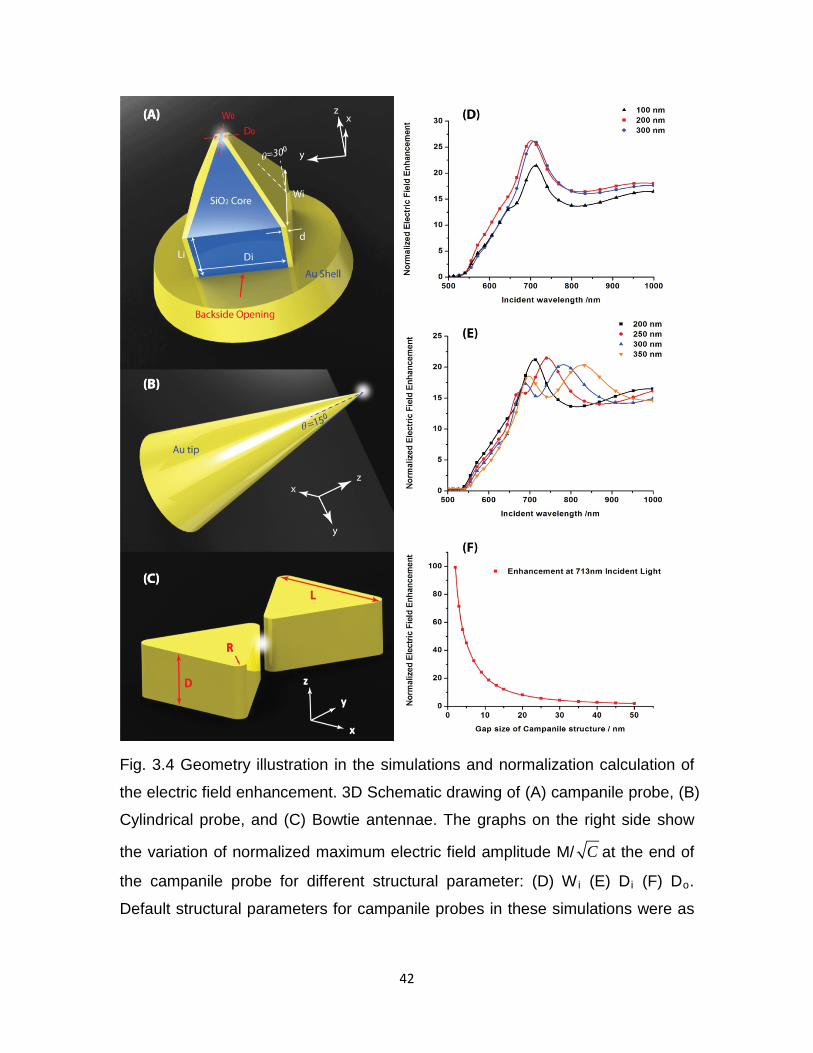
42
Fig. 3.4 Geometry illustration in the simulations and normalization calculation of
the electric field enhancement. 3D Schematic drawing of (A) campanile probe, (B)
Cylindrical probe, and (C) Bowtie antennae. The graphs on the right side show
the variation of normalized maximum electric field amplitude M/ at the end of
the campanile probe for different structural parameter: (D) Wi (E) Di (F) Do.
Default structural parameters for campanile probes in these simulations were as
C
43
follows: d=50 nm, =30o, Wo=20 nm, Li=200 nm, Wi=100 nm, Do=10 nm,
Di=200 nm.
Coupling efficiencies between far-field and near-field
Scattering losses during propagation are minimized since the plasmons travel along the smooth inner dielectric/metal interfaces. More recently, calculations have suggested that the 3D linear tapering approach could focus 830 nm light into a 2-by-5 nm2 area with ≤ 3 dB loss (3).
Campanile probe fabrication
3M single mode optical fibers for 633 nm (2.5 µm core diameter) were wet-etched with concentrated HF to shape a smooth cone with a tip radius of 100 nm. Using Focused Ion Beam (FIB) milling (Zeiss Crossbeam 1540), the campanile geometry was carved into the etched glass fiber tip. Using shadow evaporation, 50 nm thick Au with a 2nm adhesion layer was evaporated on two opposing sides of the campanile structure. Typically the resolution of the angle resolved evaporation was not sufficient to create a well-defined gap between the two triangular plates at the tip apex. Hence, a gap was cut at the tip apex, using FIB, resulting in a gap typically 40-50 nm wide and 30 nm long, as shown in Figure 3.2B. The fabrication resolution can be increased by optimizing the milling process, alternative fabrication procedures or by using a Helium FIB. For the measurements presented here 7 fibers were produced and all of them worked.
Sample preparation
The indium phosphide nanowires were prepared by Chemical Vapor Deposition (MOCVD) using Trimethylindium (TMI) and tertbutylphosphine (TBP) as In and P sources respectively. The nanowires were grown on a Si(111) substrate with a 2 nm thick gold film acting as catalyst for the nanowire formation. The substrate was annealed in-situ at 600 deg C prior to the introduction of the TMI and TBP resulting in a distribution of 10-20 nm in diameter gold clusters on the surface. The nanowires were grown at 4150 C for 10 minutes with an In molar fraction of ~2 x 10⁻⁶, V/III ratio of 40, and under a total flow of 8 l/min of H2. The as grown substrates consist of 1- 5 µm long and 30-100 nm thick nanowires. TEM analysis shows that the wires have a zinc blend structure and grow in the [111] direction with clean and often atomically flat cleaved ends. The nanowires single crystals are covered with a very thin (~ 1nm) thick amorphous layer most from oxidation in air. Their shapes are mostly cylindrical with a minority that exhibits some faceting resulting in hexagonal cross-sections.
θ
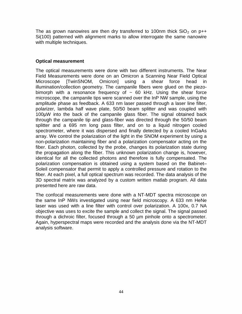
44
The as grown nanowires are then dry transferred to 100nm thick SiO2 on p++ Si(100) patterned with alignment marks to allow interrogate the same nanowire with multiple techniques.
Optical measurement
The optical measurements were done with two different instruments. The Near Field Measurements were done on an Omicron a Scanning Near Field Optical Microscope [TwinSNOM, Omicron] using a shear force head in illumination/collection geometry. The campanile fibers were glued on the piezo-bimorph with a resonance frequency of ~ 60 kHz. Using the shear force microscope, the campanile tips were scanned over the InP NW sample, using the amplitude phase as feedback. A 633 nm laser passed through a laser line filter, polarizer, lambda half wave plate, 50/50 beam splitter and was coupled with 100µW into the back of the campanile glass fiber. The signal obtained back through the campanile tip and glass-fiber was directed through the 50/50 beam splitter and a 695 nm long pass filter, and on to a liquid nitrogen cooled spectrometer, where it was dispersed and finally detected by a cooled InGaAs array. We control the polarization of the light in the SNOM experiment by using a non-polarization maintaining fiber and a polarization compensator acting on the fiber. Each photon, collected by the probe, changes its polarization state during the propagation along the fiber. This unknown polarization change is, however, identical for all the collected photons and therefore is fully compensated. The polarization compensation is obtained using a system based on the Babinet–Soleil compensator that permit to apply a controlled pressure and rotation to the fiber. At each pixel, a full optical spectrum was recorded. The data analysis of the 3D spectral matrix was analyzed by a custom written matlab program. All data presented here are raw data.
The confocal measurements were done with a NT-MDT spectra microscope on the same InP NWs investigated using near field microscopy. A 633 nm HeNe laser was used with a line filter with control over polarization. A 100x, 0.7 NA objective was uses to excite the sample and collect the signal. The signal passed through a dichroic filter, focused through a 50 µm pinhole onto a spectrometer. Again, hyperspectral maps were recorded and the analysis done via the NT-MDT analysis software.
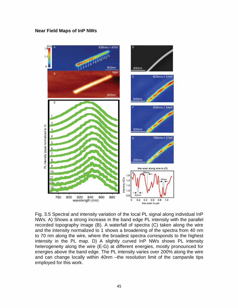
45
Near Field Maps of InP NWs
Fig. 3.5 Spectral and intensity variation of the local PL signal along individual InP NWs. A) Shows a strong increase in the band edge PL intensity with the parallel recorded topography image (B). A waterfall of spectra (C) taken along the wire and the intensity normalized to 1 shows a broadening of the spectra from 40 nm to 70 nm along the wire, where the broadest spectra corresponds to the highest intensity in the PL map. D) A slightly curved InP NWs shows PL intensity heterogeneity along the wire (E-G) at different energies, mostly pronounced for energies above the band edge. The PL intensity varies over 200% along the wire and can change locally within 40nm –the resolution limit of the campanile tips employed for this work.
46
References 1. R. Hillenbrand, T. Taubner, F. Keilmann, , Phonon-enhanced light matter interaction at the nanometre scale. Nature 418, 159 (2002).
2. L. Novotny, B. Hecht, Principles of Nano-Optics. (Cambridge University Press, 2006).
3. S. Kawata, Y. Inouye, P. Verma, , Plasmonics for near-field nano-imaging and superlensing. Nature Photonics 3, 388 (2009).
4. D. Zhang et al., Nanoscale spectroscopic imaging of organic semiconductor films by plasmon-polariton coupling. Phys. Rev. Lett. 104, 056601 (2010).
5. J. Stadler, T. Schmid, R. Zenobi, Developments in and practical guidelines for tip-enhanced Raman spectroscopy. Nanoscale 4, 1856 (2012).
6. Y. Wang, W. Srituravanich, C. Sun, X. Zhang, Plasmonic nearfield scanning probe with high transmission. Nano Letters 8, 3041 (Sep, 2008).
7. J. N. Farahani, D. W. Pohl, H. J. Eisler, B. Hecht, Single quantum dot coupled to a scanning optical antenna: A tunable superemitter. Physical Review Letters 95, 017402 (Jul, 2005).
8. A. Weber-Bargioni et al., Hyperspectral nanoscale imaging on dielectric substrates with coaxial optical antenna scan probes. Nano Letters 11, 1201 (2011).
9. D. Roy, J. Wang, C. Williams, Novel methodology for estimating the enhancement factor for tip-enhanced Raman spectroscopy. Journal of App. Phys. 105, 013530 (2009).
10. C. C. Neacsu et al., Near-field localization in plasmonic superfocusing: A nanoemitter on a tip. Nano Letters 10, 592 (Feb, 2010).
11. F. De Angelis et al., Nanoscale chemical mapping using three-dimensional adiabatic compression of surface plasmon polaritons. Nature Nanotechnol. 5, 67 (Jan, 2010).
12. M. Staffaroni, J. Conway, S. Vedantam, J. Tang, E. Yablonovitch, Photonics and Nanostructures - Fundamentals and Applications 10, 166 (2012).
13. M. I. Stockman, Nanofocusing of optical energy in tapered plasmonic waveguides. Phys. Rev. Lett. 93, 137404 (2004).
14. P. Ginzburg, D. Arbel, M. Orenstein, Gap plasmon polariton structure for very efficient microscale-to-nanoscale interfacing. Opt. Lett. 31, 3288 (Nov 15, 2006).
47
15. S. Vedantam et al., A plasmonic dimple lens for nanoscale focusing of light Nano Lett. 9, 3447 (Oct, 2009).
16. E. Peytavit, J. F. Lampin, T. Akalin, L. Desplanque, Integrated terahertz TEM horn antenna. Electron. Lett. 43, 73 (Jan, 2007).
17. J. F. Wang, M. S. Gudiksen, X. F. Duan, Y. Cui, C. M. Lieber, Highly polarized photoluminescence and photodetection from single indium phosphide nanowires. Science 293, 1455 (2001).
18. J. M. Bao et al., Optical properties of rotationally twinned InP nanowire heterostructures. Nano Lett. 8, 836 (2008).
19. K. Cho et al., Molecular monolayers for conformal, nanoscale doping of InP nanopillar photovoltaics. App. Phys. Lett. 98, (2011).
20. A. Franceschetti, A. Zunger, Optical transitions in charged CdSe quantum dots. Phys. Rev. B 62, R16287 (Dec 15, 2000).
21. S. A. Fischer, C. M. Isborn, O. V. Prezhdo, Excited states and optical absorption of small semiconducting clusters: Dopants, defects and charging. Chemical Science 2, 400 (2011).
22. L. K. van Vugt, S. J. Veen, E. P. A. M. Bakkers, A. L. Roest, D. Vanmaekelbergh, Increase of the photoluminescence intensity of InP nanowires by photoassisted surface passivation. J. Am. Chem. Soc. 127, 12357 (2005).
23. N. Yamamoto, S. Bhunia, Y. Watanabe, Polarized cathodoluminescence study of InP nanowires by transmission electron microscopy. App. Phys. Lett. 88, (2006).
24. E. Shafran, B. D. Mangum, J. M. Gerton, Using the near-field coupling of a sharp tip to tune fluorescence-emission fluctuations during quantum-dot blinking. PRL 107, 037403 (2011).
25. J. J. Greffet, Applied physics. Nanoantennas for light emission. Science 308, 1561 (2005).
26. S. Kuhn, U. Hkanson, L. Rogobete, V. Sandoghdar, Enhancement of single-molecule fluorescence using a gold nanoparticle as an optical nanoantenna. PRL 97, 017402 (2006).
27. H. J. Maas et al., Imaging of photonic nanopatterns by scanning near-field optical microscopy. J. Opt. Soc. Am. B-Opt. Phys. 19, 1295 (2002).
28. M. L. M. Balistreri, H. Gersen, J. P. Korterik, L. Kuipers, N. F. van Hulst, Tracking femtosecond laser pulses in space and time. Science 294, 1080 (2001).

48
29. P. Vasa, C. Ropers, R. Pomraenke, C. Lienau, Ultra-fast nano-optics. Laser Photon. Rev. 3, 483 (2009).
30. M. Seo et al., Active terahertz nanoantennas based on VO2 phase transition. Nano Lett. 10, 2064 (2010).
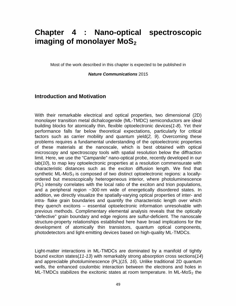
49
Chapter 4 : Nano-optical spectroscopic imaging of monolayer MoS2
Most of the work described in this chapter is expected to be published in
Nature Communications 2015 Introduction and Motivation
With their remarkable electrical and optical properties, two dimensional (2D) monolayer transition metal dichalcogenide (ML-TMDC) semiconductors are ideal building blocks for atomically thin, flexible optoelectronic devices(1-8). Yet their performance falls far below theoretical expectations, particularly for critical factors such as carrier mobility and quantum yield(2, 9). Overcoming these problems requires a fundamental understanding of the optoelectronic properties of these materials at the nanoscale, which is best obtained with optical microscopy and spectroscopy tools with spatial resolution below the diffraction limit. Here, we use the “Campanile” nano-optical probe, recently developed in our lab(10), to map key optoelectronic properties at a resolution commensurate with characteristic distances such as the exciton diffusion length. We find that synthetic ML-MoS2 is composed of two distinct optoelectronic regions: a locally-ordered but mesoscopically heterogeneous interior, where photoluminescence (PL) intensity correlates with the local ratio of the exciton and trion populations, and a peripheral region ~300 nm wide of energetically disordered states. In addition, we directly visualize the spatially-varying optical properties of inter- and intra- flake grain boundaries and quantify the characteristic length over which they quench excitons – essential optoelectronic information unresolvable with previous methods. Complimentary elemental analysis reveals that the optically “defective” grain boundary and edge regions are sulfur-deficient. The nanoscale structure-property relationships established here have broad implications for the development of atomically thin transistors, quantum optical components, photodetectors and light-emitting devices based on high-quality ML-TMDCs.
Light-matter interactions in ML-TMDCs are dominated by a manifold of tightly bound exciton states(11-13) with remarkably strong absorption cross sections(14) and appreciable photoluminescence (PL)(15, 16). Unlike traditional 2D quantum wells, the enhanced coulombic interaction between the electrons and holes in ML-TMDCs stabilizes the excitonic states at room temperature. In ML-MoS2 the
50
most prevalent states are the low energy A exciton and the charged A- trion state(17). The balance of trions and excitons can be tuned by gating, which changes the electron density in the material(17). Furthermore, adsorbates(18), strain(19, 20) and piezoelectric(5) effects can reversibly modify the energy of excitonic states, whereas structural discontinuities such as grain boundaries(21) and defects(18) can enhance or quench luminescence. Although these tunable excitonic states are attractive for device and sensing applications, they are easily perturbed, and their spatial variability at nanometer length scales has been largely neglected. While scanning tunneling(22, 23) and transmission electron (21, 24, 25) microscopies have probed atomic scale electronic properties and structural defects, to date optical investigations have been diffraction-limited. Near-field optical microscopy provides a route to explore material properties below the diffraction limit(26-28). However, nanometer scale optical visualization and spectroscopy of inelastic light-matter interactions (such as nano-PL) in 2D TMDC systems constitutes a formidable challenge necessitating a non-traditional approach that confines optical excitation and collection without hindering detailed spectral analysis. Here, the sub-diffraction hyperspectral imaging capability of the Campanile probes allows us to differentiate the optoelectronic properties of the interior, edge and grain boundary regions of individual flakes of ML-MoS2.
51
Fig. 4.1. Nano-optical imaging of PL in ML-MoS2. a. Illustration of near-field excitation and collection of the PL from ML-MoS2 using the Campanile near-field probe where the optical laser excitation (2.33 eV) and collection of sample emission are confined to the apex of the tip(10) to produce optical maps with ~60 nm resolution. At each pixel a full PL spectrum is acquired. b. Normalized PL emission intensity map of a triangular ML-MoS2 flake using the Campanile probe. The white dashed line indicates the flake boundary as determined from the shear-force topography. c. An image of the same flake acquired with scanning confocal microscopy using a 100×, 0.7 NA air objective. d. Near-field nano-PL spectrum averaged over the spatial extent of the ML-MoS2 flake. The emission contains two peaks arising from the radiative recombination from exciton and trion states. The dashed vertical line shows the position of the spectral median (SM) that splits the spectrum into equal amounts of high and low energy counts and is used to quantify spectral variations in the lower signal-to-noise spectra of individual spatial positions acquired during fast scans. All data were acquired under ambient conditions.
52
Results and Discussions Compared to ML-TMDCs produced by exfoliation from bulk crystals, CVD-grown ML-TMDCs are appealing for device applications where high-yield and large area production is required. Figure 4.1a illustrates hyperspectral near-field microscopy of CVD-grown ML-MoS2. With the Campanile probe, optical excitation and collection are spatially confined to the nanogap at the apex of the tip, which is scanned over the sample, recording a full emission spectrum at each position(10). The spatial distribution of the integrated PL intensity (Fig. 4.1b) exhibits nanoscale fluctuations that are unresolved in the conventional confocal optical microscopy image of the same flake (Fig. 4.1c). The emission arises from the radiative recombination of the A exciton at ~1.84 eV, and its A- trion at ~1.81 eV, which overlap strongly, as shown in Figure 4.1d. To simply describe the energetic distribution of the PL at each position (where the per-pixel data is more noisy than the average spectrum shown in Fig. 1d), we use the “spectral median” (SM) of the emission, which divides the spectrum into low and high-energy regions of equal intensity. The SM captures overall spectral variations at each spatial position in a single value.
A nano-PL map of another MoS2 flake is shown in Figure 4.2. Spatial variations in the intensity (Fig. 4.2a) and emission energy (Fig. 4.2b) are observed across the flake (simultaneously-collected topographic images indicate that these are not topographical artefacts). Additionally, it is clear that the PL intensity weakens near the edges. By systematically analyzing the spectra as a function of distance from the flake boundaries, a distinct edge region ~300 nm wide is revealed (see Fig. 4.12 for details of the analysis). Figure 4.2c shows a correlation plot between the emission energy and intensity for the interior and edge areas, showing that the two regions exhibit different behavior. In the interior region, the intensity and energy of the PL are visibly correlated (orange data points), with the higher-energy emission tending to be brightest. In contrast, the edge data (blue data points) are more disordered, spanning nearly the entire range of emission energies at the lower emission intensities.
To explore the correlation between the spatially-varying intensity and spectral distribution, the emission spectra are grouped by their total emission intensity into one of 5 ranges (ranges I, II, III, IV, and V in Fig. 4.2c). The average emission spectrum for each of these intensity ranges is shown in Figure 4.2d and 4.2e for the interior and edge regions, respectively. In the interior, we see that the spectral variation is due to fluctuations of the relative intensity of the low energy emission, which originates from the trion states (Fig. 4.1d); i.e., the correlated spectral and intensity variations are related to the relative trion population. This trend is consistent with localized regions of increased carrier density that
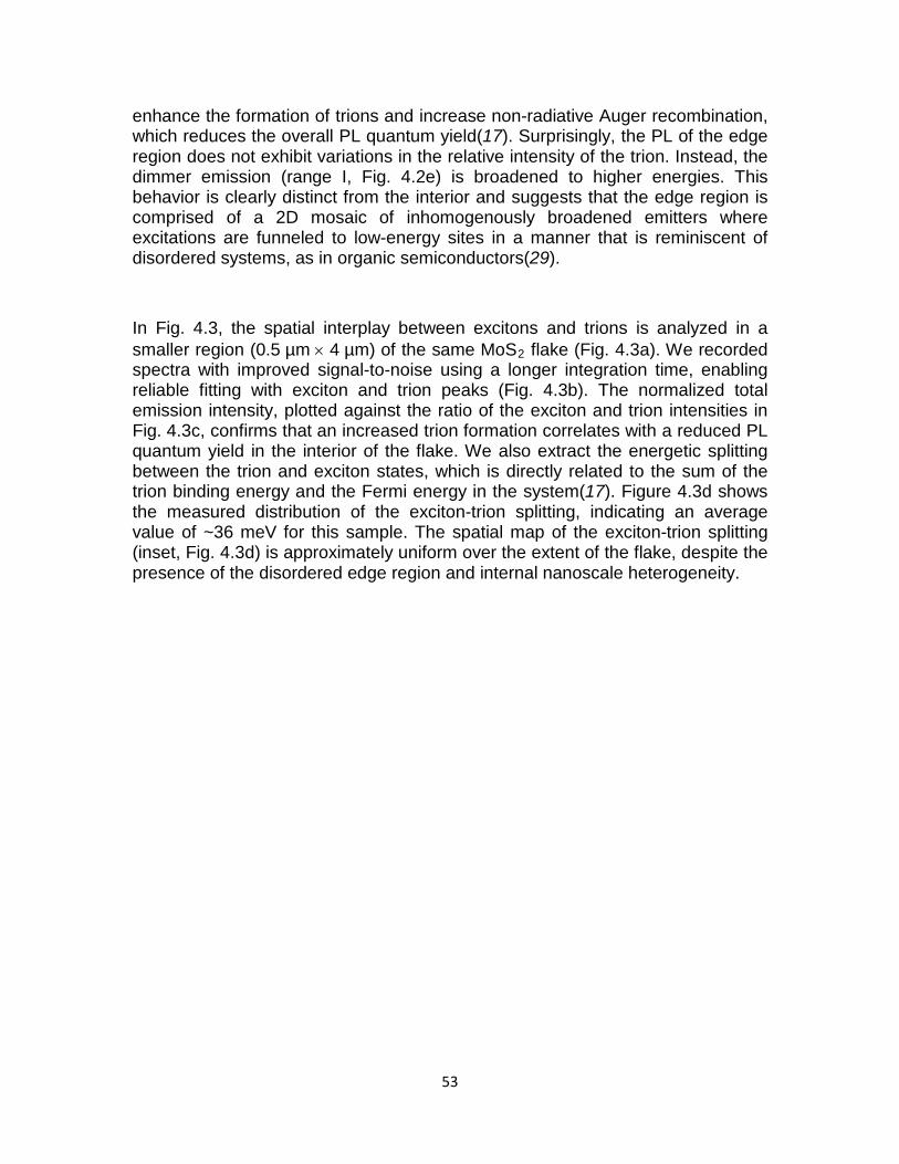
53
enhance the formation of trions and increase non-radiative Auger recombination, which reduces the overall PL quantum yield(17). Surprisingly, the PL of the edge region does not exhibit variations in the relative intensity of the trion. Instead, the dimmer emission (range I, Fig. 4.2e) is broadened to higher energies. This behavior is clearly distinct from the interior and suggests that the edge region is comprised of a 2D mosaic of inhomogenously broadened emitters where excitations are funneled to low-energy sites in a manner that is reminiscent of disordered systems, as in organic semiconductors(29).
In Fig. 4.3, the spatial interplay between excitons and trions is analyzed in a smaller region (0.5 µm × 4 µm) of the same MoS2 flake (Fig. 4.3a). We recorded spectra with improved signal-to-noise using a longer integration time, enabling reliable fitting with exciton and trion peaks (Fig. 4.3b). The normalized total emission intensity, plotted against the ratio of the exciton and trion intensities in Fig. 4.3c, confirms that an increased trion formation correlates with a reduced PL quantum yield in the interior of the flake. We also extract the energetic splitting between the trion and exciton states, which is directly related to the sum of the trion binding energy and the Fermi energy in the system(17). Figure 4.3d shows the measured distribution of the exciton-trion splitting, indicating an average value of ~36 meV for this sample. The spatial map of the exciton-trion splitting (inset, Fig. 4.3d) is approximately uniform over the extent of the flake, despite the presence of the disordered edge region and internal nanoscale heterogeneity.
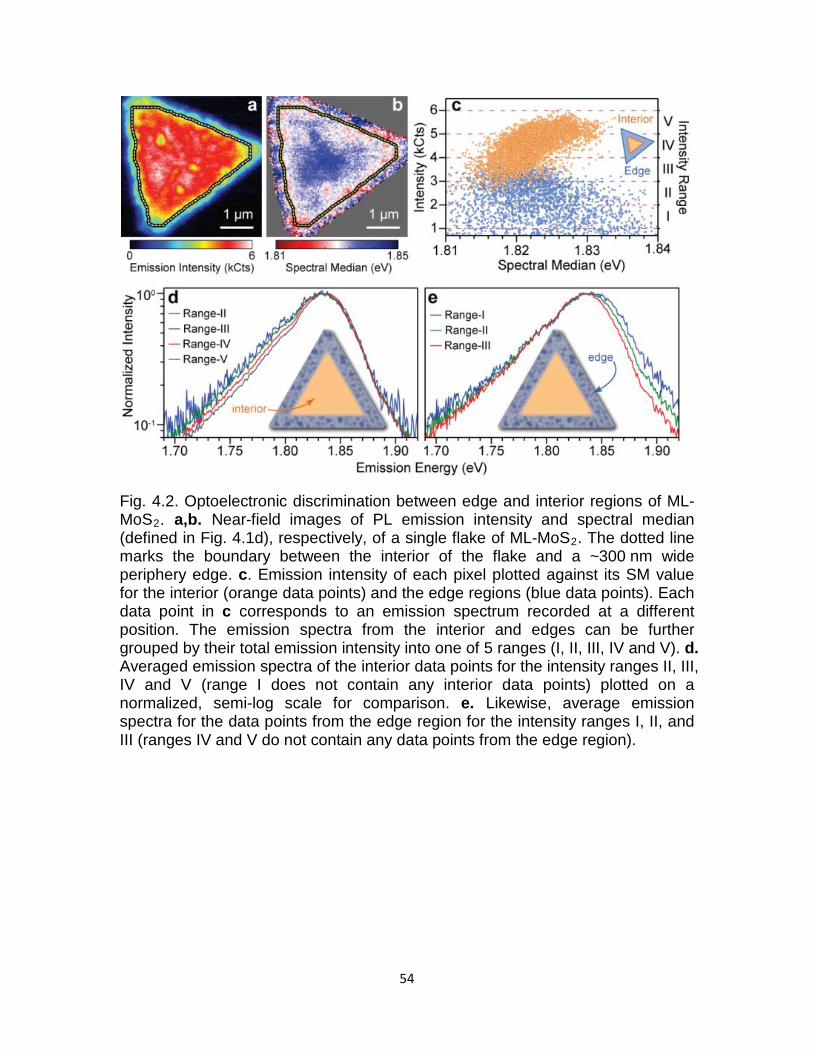
54
Fig. 4.2. Optoelectronic discrimination between edge and interior regions of ML-MoS2. a,b. Near-field images of PL emission intensity and spectral median (defined in Fig. 4.1d), respectively, of a single flake of ML-MoS2. The dotted line marks the boundary between the interior of the flake and a ~300 nm wide periphery edge. c. Emission intensity of each pixel plotted against its SM value for the interior (orange data points) and the edge regions (blue data points). Each data point in c corresponds to an emission spectrum recorded at a different position. The emission spectra from the interior and edges can be further grouped by their total emission intensity into one of 5 ranges (I, II, III, IV and V). d. Averaged emission spectra of the interior data points for the intensity ranges II, III, IV and V (range I does not contain any interior data points) plotted on a normalized, semi-log scale for comparison. e. Likewise, average emission spectra for the data points from the edge region for the intensity ranges I, II, and III (ranges IV and V do not contain any data points from the edge region).
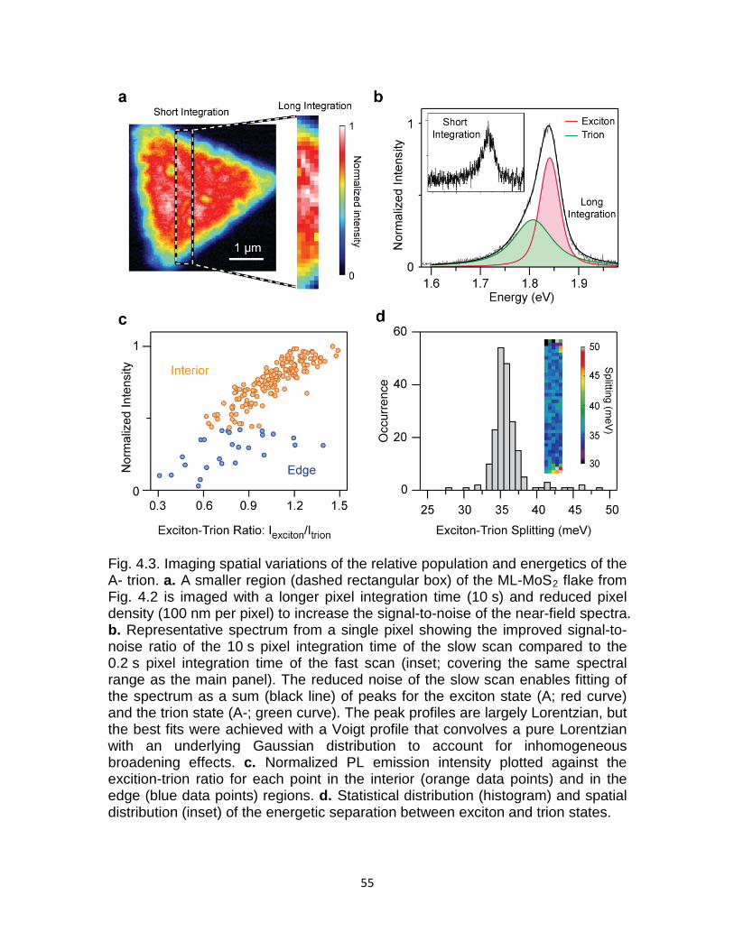
55
Fig. 4.3. Imaging spatial variations of the relative population and energetics of the A- trion. a. A smaller region (dashed rectangular box) of the ML-MoS2 flake from Fig. 4.2 is imaged with a longer pixel integration time (10 s) and reduced pixel density (100 nm per pixel) to increase the signal-to-noise of the near-field spectra. b. Representative spectrum from a single pixel showing the improved signal-to-noise ratio of the 10 s pixel integration time of the slow scan compared to the 0.2 s pixel integration time of the fast scan (inset; covering the same spectral range as the main panel). The reduced noise of the slow scan enables fitting of the spectrum as a sum (black line) of peaks for the exciton state (A; red curve) and the trion state (A-; green curve). The peak profiles are largely Lorentzian, but the best fits were achieved with a Voigt profile that convolves a pure Lorentzian with an underlying Gaussian distribution to account for inhomogeneous broadening effects. c. Normalized PL emission intensity plotted against the excition-trion ratio for each point in the interior (orange data points) and in the edge (blue data points) regions. d. Statistical distribution (histogram) and spatial distribution (inset) of the energetic separation between exciton and trion states.

56
Internal disruptions to the crystalline structure of MoS2 can occur during the CVD growth process. Isolated MoS2 flakes can form intricate star-like structures while multi-flake aggregates form a complex polycrystalline system20,24. Figure 4.4 shows both confocal and nano-PL data from three MoS2 flakes (labeled 1, 2, and 3) that merged during growth. Although the confocal optical microscopy image (Fig. 4.4a) exhibits a mostly-uniform PL intensity distribution within each flake, indicating a “high quality” sample, substantial nanoscale fluctuations are observed in the nano-PL image. Furthermore, in the nano-PL scan, a more pronounced reduction in the PL intensity marks the boundaries between flakes 1 and 2 as well as flakes 2 and 3 (Fig. 4.4b). In addition to the interflake boundaries, three narrow regions can be observed where the PL is quenched by ~20% extending radially from the center of flake 1 (also in flake 3 and others shown in the SI). Interestingly these grain boundaries do not seem to alter the energetics of the PL, as can be observed in the map of the emission energy in Fig. 4.4c, which is devoid of similar features.
The structural extent of a grain boundary has a characteristic width of the order of the lattice spacing20,24. If the atomic scale region defining the grain boundary serves as a non-radiative recombination center20, its optoelectronic width will be determined by the exciton diffusion length (estimated to be 24 nm20) as well as by the width of local band bending or carrier depletion zones. Thus, the observed width reflects a convolution of the optoelectronic properties of the grain boundaries, exciton diffusion length and the imaging resolution. The spatial resolution of the Campanile probe is determined by the nanoscale gap at the tip apex10 and the smallest features observed in these scans are ~60 nm in size, establishing an upper bound on our resolution (see SI for resolution analysis and tip details). By measuring the widths of the edge and grain boundary regions we can establish an upper bound on the average extent of the optoelectronic region of 150 nm for the interflake boundaries and 125 nm for the intraflake defects, with a variability of about 100 nm (Fig. 4.4d).
Interestingly, nano-Auger spectroscopy maps of ML-MoS2 flakes from the same CVD growth run, shown in Fig. 4.4e (and Fig. 4.14), reveal that the grain boundaries and edge regions are S deficient. This is consistent with previous results that show a “Mo rich” edge23. Such S-deficient regions in MoS2 suggest probable n-doping near these boundaries20, and also are suspected to have a higher density of mid-gap trap states20,23, which offers an explanation for the observed reduction in PL quantum yield.
Previous work on epitaxially grown ML-MoS2 has shown that an atomic metallic edge state is formed at the boundary of the flakes21. Here we show that CVD-grown MoS2 flakes are enclosed by a larger disordered, S-deficient edge region.

57
We hypothesize that this edge forms during the termination of the growth process (i.e., the cooling step) producing the defective region23. Together, these results may help to explain observed edge-related effects such as resonantly enhanced second harmonic generation30, and have significant implications on carrier mobility in MoS2 where both hopping and band transport mechanisms have been reported9. It is likely that hopping mechanisms dominate in the disordered edge area as opposed to high mobility band transport in the interior.
58
Fig. 4.4. Excited state quenching of grain boundaries and elemental mapping of ML-MoS2. a,b. Far-field confocal microscopy PL intensity image (a) and normalized nano-PL intensity map (b) of an aggregate of three flakes (labeled 1, 2 and 3) forming three interflake grain boundaries. In the interior of flake 1, radial intraflake grain boundaries are observed extending from the center towards the apexes of the triangular flake. The interflake boundary quenches the PL intensity by 50-80%, whereas the intraflake boundary quenches the PL intensity by ~20%. c. Map of the emission energy (i.e., the SM value defined in Fig. 4.1d). d. Histograms of the half-width-at-half-max (HWHM) sizes of the interflake and intraflake grain boundaries, which are measured from the spatial extent of the PL reduction and sampled semi-equidistantly along the respective features (see Fig. 4.13 for more details). e. Nano-Auger elemental mapping of S and Mo on a similar multiflake aggregate from the same growth run. Both the edge region and grain boundaries are sulfur-deficient while the Mo composition is uniform over the flakes.
59
Conclusion
Altogether, our results provide a new picture of the rich optoelectronic properties of CVD-grown ML-MoS2. In particular, the intraflake grain boundaries and the ~300 nm disordered edge region of localized recombination centers discovered here are expected to have substantial effects on device performance, especially carrier mobility and recombination. Since grain-boundary quenching is limited to ~150 nm, it may be relatively unimportant for micron-sized optoelectronic devices. Detailed information on the subtle variations in optoelectronic properties and their relationship to corresponding nanometer scale structures within synthetic ML-TMDCs can guide the future development of high quality 2D materials and next-generation devices.

60
Materials and Methods
Fabrication details for the Campanile probe
For a single Campanile tip, a Nufern S630-HP pure silica core single mode optical fiber (3.5 μm core diameter) was wet etched with 40% HF to shape a smooth cone with a half-cone-angle of ~18° and a tip-radius that is less than 200 nm. A 300 nm thick layer of a mixture of Pt and Au was sputtered on the fiber surface to ensure high conductivity in Ga+ focused ion beam (FIB) milling (Zeiss Crossbeam 1540) process. The preliminary Campanile geometry was carved into the etched glass fiber tip by FIB milling. A subsequent 300 nm Pt/Au layer was deposited via sputtering to recoat the newly exposed SiO2 surfaces with a conductive metal. A second FIB milling process is used to expose two opposing sides of the Campanile structure. Using tilt evaporation at 24°, a 3 nm Ti adhesion layer followed by a 70 nm thick Au layer and finally a 20 nm thick Cr protection layer were evaporated onto the structure on the SiO2 surfaces exposed in the second FIB milling step to form the opposing metallic plates of the Campanile structure. After a final milling step to refine the shape and ensure that the metal plates are not connected, Cr etchant was used to strip the superfluous Cr layers, and finally 2 nm thick layer of Al2O3 was deposited on the structure by atomic layer deposition at 40 °C. SEM micrographs of the final Campanile structures are shown in Fig. 4.5. Typically the resolution of the angle resolved evaporation was not sufficient to create a well-defined gap between the two triangular metallic plates at the apex. Thus, the gap was further cut using FIB milling, yielding gap with dimensions that were typically 35-40 nm wide and 50 nm long (Fig. 4.5).
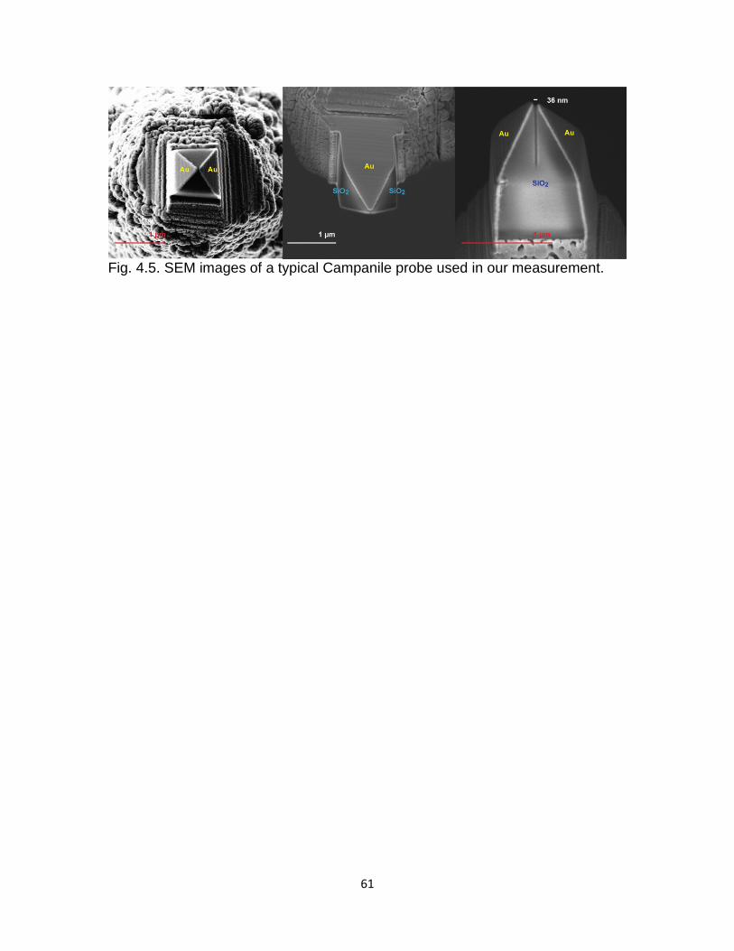
61
Fig. 4.5. SEM images of a typical Campanile probe used in our measurement.
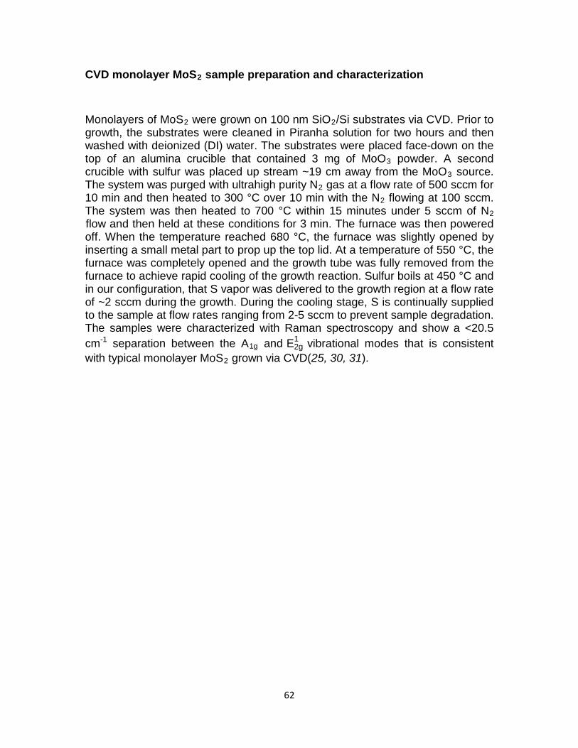
62
CVD monolayer MoS2 sample preparation and characterization
Monolayers of MoS2 were grown on 100 nm SiO2/Si substrates via CVD. Prior to growth, the substrates were cleaned in Piranha solution for two hours and then washed with deionized (DI) water. The substrates were placed face-down on the top of an alumina crucible that contained 3 mg of MoO3 powder. A second crucible with sulfur was placed up stream ~19 cm away from the MoO3 source. The system was purged with ultrahigh purity N2 gas at a flow rate of 500 sccm for 10 min and then heated to 300 °C over 10 min with the N2 flowing at 100 sccm. The system was then heated to 700 °C within 15 minutes under 5 sccm of N2 flow and then held at these conditions for 3 min. The furnace was then powered off. When the temperature reached 680 °C, the furnace was slightly opened by inserting a small metal part to prop up the top lid. At a temperature of 550 °C, the furnace was completely opened and the growth tube was fully removed from the furnace to achieve rapid cooling of the growth reaction. Sulfur boils at 450 °C and in our configuration, that S vapor was delivered to the growth region at a flow rate of ~2 sccm during the growth. During the cooling stage, S is continually supplied to the sample at flow rates ranging from 2-5 sccm to prevent sample degradation. The samples were characterized with Raman spectroscopy and show a <20.5 cm-1 separation between the A1g and E2g
1 vibrational modes that is consistent with typical monolayer MoS2 grown via CVD(25, 30, 31).
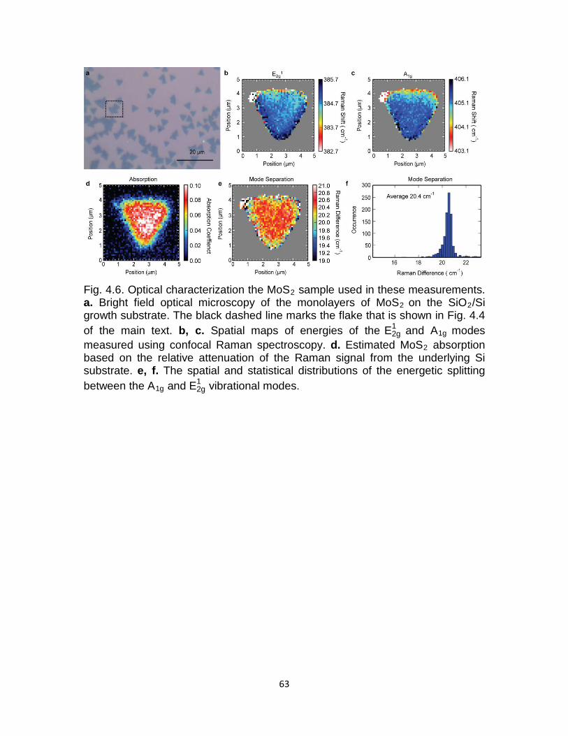
63
Fig. 4.6. Optical characterization the MoS2 sample used in these measurements. a. Bright field optical microscopy of the monolayers of MoS2 on the SiO2/Si growth substrate. The black dashed line marks the flake that is shown in Fig. 4.4 of the main text. b, c. Spatial maps of energies of the E2g
1 and A1g modes measured using confocal Raman spectroscopy. d. Estimated MoS2 absorption based on the relative attenuation of the Raman signal from the underlying Si substrate. e, f. The spatial and statistical distributions of the energetic splitting between the A1g and E2g
1 vibrational modes.
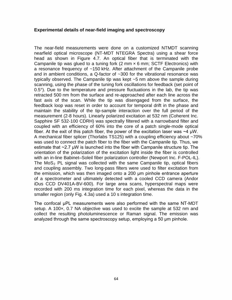
64
Experimental details of near-field imaging and spectroscopy
The near-field measurements were done on a customized NTMDT scanning nearfield optical microscope (NT-MDT NTEGRA Spectra) using a shear force head as shown in Figure 4.7. An optical fiber that is terminated with the Campanile tip was glued to a tuning fork (2 mm × 6 mm; SCTF Electronics) with a resonance frequency of ~150 kHz. After attachment of the Campanile probe and in ambient conditions, a Q-factor of ~300 for the vibrational resonance was typically observed. The Campanile tip was kept ~5 nm above the sample during scanning, using the phase of the tuning fork oscillations for feedback (set point of 0.5°). Due to the temperature and pressure fluctuations in the lab, the tip was retracted 500 nm from the surface and re-approached after each line across the fast axis of the scan. While the tip was disengaged from the surface, the feedback loop was reset in order to account for temporal drift in the phase and maintain the stability of the tip-sample interaction over the full period of the measurement (2-8 hours). Linearly polarized excitation at 532 nm (Coherent Inc. Sapphire SF 532-100 CDRH) was spectrally filtered with a narrowband filter and coupled with an efficiency of 60% into the core of a patch single-mode optical fiber. At the exit of this patch fiber, the power of the excitation laser was ~4 μW. A mechanical fiber splicer (Thorlabs TS125) with a coupling efficiency about ~70% was used to connect the patch fiber to the fiber with the Campanile tip. Thus, we estimate that ~2.7 μW is launched into the fiber with Campanile structure tip. The orientation of the polarization of the excitation light inside the fiber is controlled with an in-line Babinet–Soleil fiber polarization controller (Newport Inc. F-POL-IL). The MoS2 PL signal was collected with the same Campanile tip, optical fibers and coupling assembly. Two long-pass filters were used to filter excitation from the emission, which was then imaged onto a 200 μm pinhole entrance aperture of a spectrometer and ultimately detected with a cooled CCD camera (Andor iDus CCD DV401A-BV-600). For large area scans, hyperspectral maps were recorded with 200 ms integration time for each pixel, whereas the data in the smaller region (only Fig. 4.3a) used a 10 s integration time.
The confocal μPL measurements were also performed with the same NT-MDT setup. A 100×, 0.7 NA objective was used to excite the sample at 532 nm and collect the resulting photoluminescence or Raman signal. The emission was analyzed through the same spectroscopy setup, employing a 50 μm pinhole.
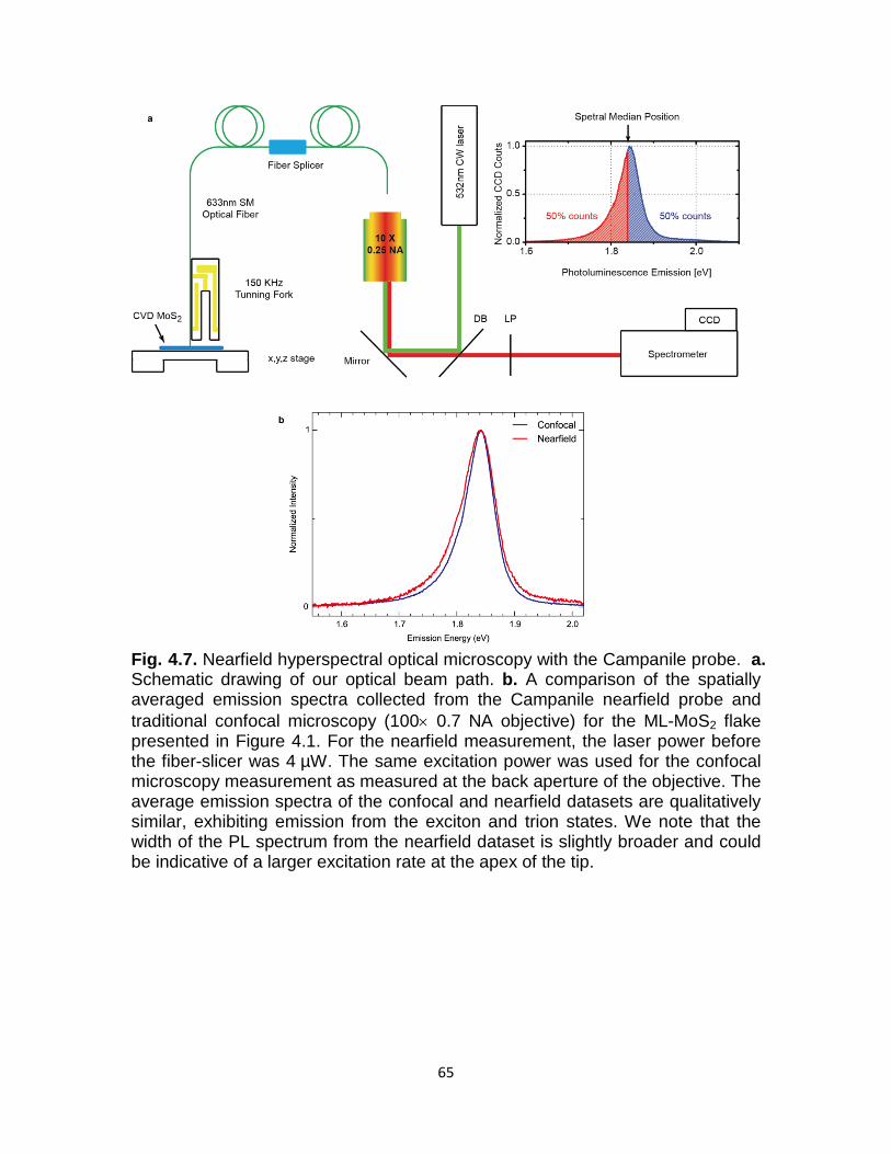
65
Fig. 4.7. Nearfield hyperspectral optical microscopy with the Campanile probe. a. Schematic drawing of our optical beam path. b. A comparison of the spatially averaged emission spectra collected from the Campanile nearfield probe and traditional confocal microscopy (100× 0.7 NA objective) for the ML-MoS2 flake presented in Figure 4.1. For the nearfield measurement, the laser power before the fiber-slicer was 4 µW. The same excitation power was used for the confocal microscopy measurement as measured at the back aperture of the objective. The average emission spectra of the confocal and nearfield datasets are qualitatively similar, exhibiting emission from the exciton and trion states. We note that the width of the PL spectrum from the nearfield dataset is slightly broader and could be indicative of a larger excitation rate at the apex of the tip.
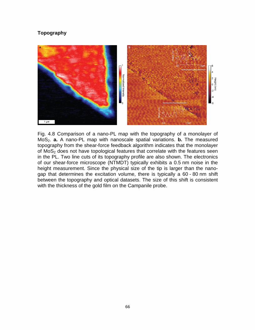
66
Topography
Fig. 4.8 Comparison of a nano-PL map with the topography of a monolayer of MoS2. a. A nano-PL map with nanoscale spatial variations. b. The measured topography from the shear-force feedback algorithm indicates that the monolayer of MoS2 does not have topological features that correlate with the features seen in the PL. Two line cuts of its topography profile are also shown. The electronics of our shear-force microscope (NTMDT) typically exhibits a 0.5 nm noise in the height measurement. Since the physical size of the tip is larger than the nano-gap that determines the excitation volume, there is typically a 60 - 80 nm shift between the topography and optical datasets. The size of this shift is consistent with the thickness of the gold film on the Campanile probe.
67
Estimate of spatial resolution
Without a single point emitter or discrete edge in the monolayer MoS2, the spatial resolution can only be estimated from the sharpest observed features, which ranged from 50-80 nm. In Figure 4.8, one such feature is extracted from the map of the PL intensity (Fig. 4.9a). Here, the feature corresponds to the transition from a dim area to a bright area (Fig. 4.9b). The spatial derivative (Fig. 4.9c) of the feature is well-described by a Gaussian peak with a full-width-a-half-maximum value of 63 nm, corresponding to a 2σ width of 54 nm. In terms of a step, the 2σ width marks the extent of transition from 15% to 84% of the step height and yields the best estimate of the spatial resolution.
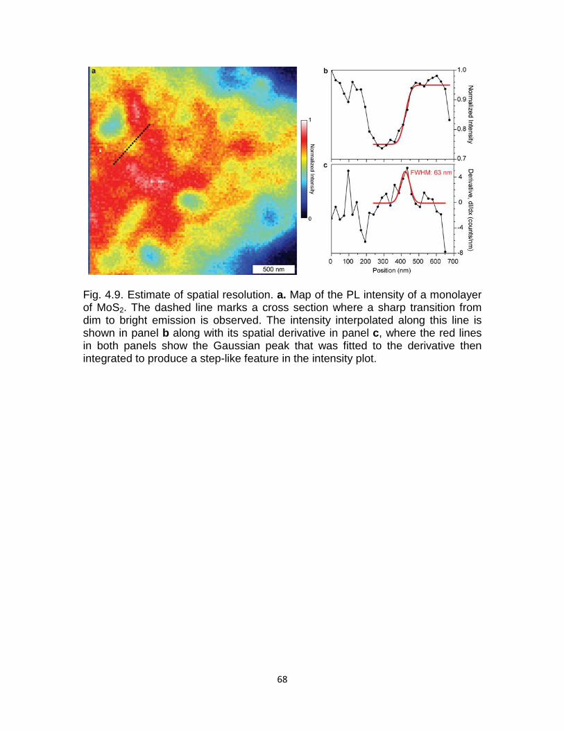
68
Fig. 4.9. Estimate of spatial resolution. a. Map of the PL intensity of a monolayer of MoS2. The dashed line marks a cross section where a sharp transition from dim to bright emission is observed. The intensity interpolated along this line is shown in panel b along with its spatial derivative in panel c, where the red lines in both panels show the Gaussian peak that was fitted to the derivative then integrated to produce a step-like feature in the intensity plot.
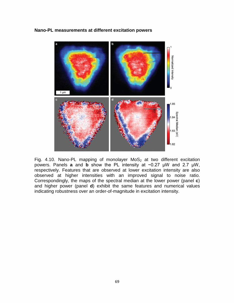
69
Nano-PL measurements at different excitation powers
Fig. 4.10. Nano-PL mapping of monolayer MoS2 at two different excitation powers. Panels a and b show the PL intensity at ~0.27 μW and 2.7 μW, respectively. Features that are observed at lower excitation intensity are also observed at higher intensities with an improved signal to noise ratio. Correspondingly, the maps of the spectral median at the lower power (panel c) and higher power (panel d) exhibit the same features and numerical values indicating robustness over an order-of-magnitude in excitation intensity.
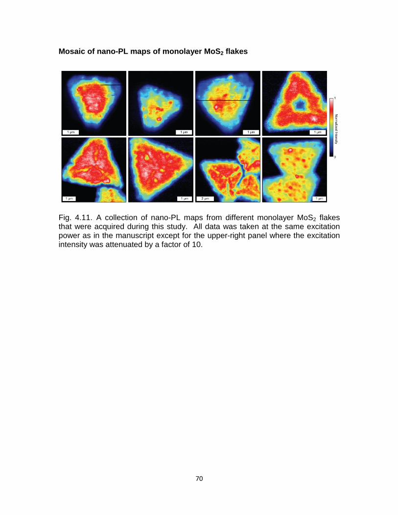
70
Mosaic of nano-PL maps of monolayer MoS2 flakes
Fig. 4.11. A collection of nano-PL maps from different monolayer MoS2 flakes that were acquired during this study. All data was taken at the same excitation power as in the manuscript except for the upper-right panel where the excitation intensity was attenuated by a factor of 10.
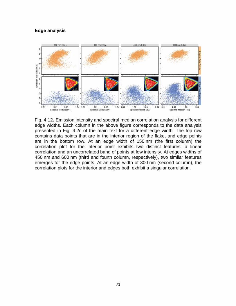
71
Edge analysis
Fig. 4.12. Emission intensity and spectral median correlation analysis for different edge widths. Each column in the above figure corresponds to the data analysis presented in Fig. 4.2c of the main text for a different edge width. The top row contains data points that are in the interior region of the flake, and edge points are in the bottom row. At an edge width of 150 nm (the first column) the correlation plot for the interior point exhibits two distinct features: a linear correlation and an uncorrelated band of points at low intensity. At edges widths of 450 nm and 600 nm (third and fourth column, respectively), two similar features emerges for the edge points. At an edge width of 300 nm (second column), the correlation plots for the interior and edges both exhibit a singular correlation.
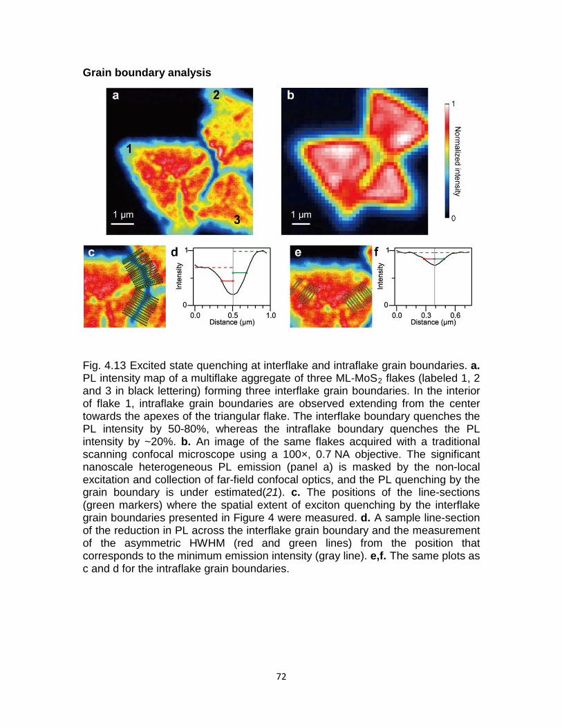
72
Grain boundary analysis
Fig. 4.13 Excited state quenching at interflake and intraflake grain boundaries. a. PL intensity map of a multiflake aggregate of three ML-MoS2 flakes (labeled 1, 2 and 3 in black lettering) forming three interflake grain boundaries. In the interior of flake 1, intraflake grain boundaries are observed extending from the center towards the apexes of the triangular flake. The interflake boundary quenches the PL intensity by 50-80%, whereas the intraflake boundary quenches the PL intensity by ~20%. b. An image of the same flakes acquired with a traditional scanning confocal microscope using a 100×, 0.7 NA objective. The significant nanoscale heterogeneous PL emission (panel a) is masked by the non-local excitation and collection of far-field confocal optics, and the PL quenching by the grain boundary is under estimated(21). c. The positions of the line-sections (green markers) where the spatial extent of exciton quenching by the interflake grain boundaries presented in Figure 4 were measured. d. A sample line-section of the reduction in PL across the interflake grain boundary and the measurement of the asymmetric HWHM (red and green lines) from the position that corresponds to the minimum emission intensity (gray line). e,f. The same plots as c and d for the intraflake grain boundaries.

73
Nano-auger characterization of edge and grain boundaries.
Nano-Auger electron spectroscopy was performed to probe local chemical composition on CVD-grown MoS2 flakes. This instrument uses a field emission electron source that enables focusing of the electron beam to a spot size of ~ 10 nm in the ultra-high vacuum chamber of base pressure ~ 10-10 mbar (Oxford/Omicron Nano-Auger system). The typical uncertainty in the nano-Auger composition measurement is ~3%.
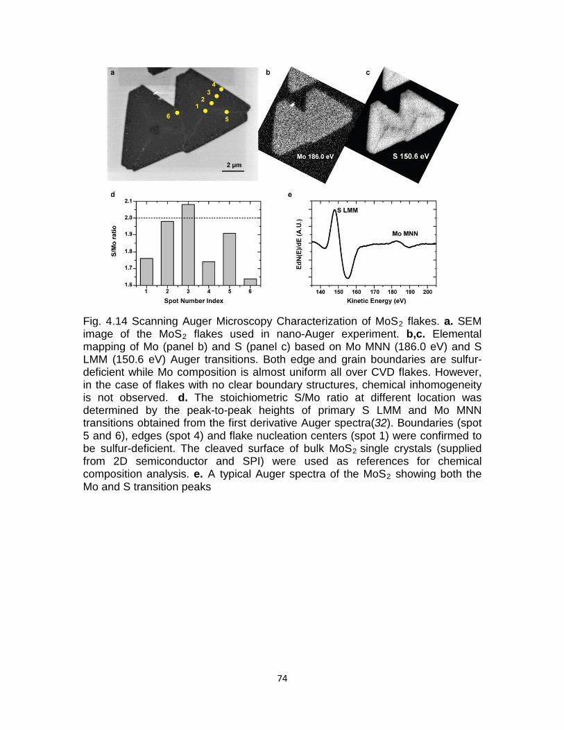
74
Fig. 4.14 Scanning Auger Microscopy Characterization of MoS2 flakes. a. SEM image of the MoS2 flakes used in nano-Auger experiment. b,c. Elemental mapping of Mo (panel b) and S (panel c) based on Mo MNN (186.0 eV) and S LMM (150.6 eV) Auger transitions. Both edge and grain boundaries are sulfur-deficient while Mo composition is almost uniform all over CVD flakes. However, in the case of flakes with no clear boundary structures, chemical inhomogeneity is not observed. d. The stoichiometric S/Mo ratio at different location was determined by the peak-to-peak heights of primary S LMM and Mo MNN transitions obtained from the first derivative Auger spectra(32). Boundaries (spot 5 and 6), edges (spot 4) and flake nucleation centers (spot 1) were confirmed to be sulfur-deficient. The cleaved surface of bulk MoS2 single crystals (supplied from 2D semiconductor and SPI) were used as references for chemical composition analysis. e. A typical Auger spectra of the MoS2 showing both the Mo and S transition peaks
75
Reference
1. B. Radisavljevic, A. Radenovic, J. Brivio, V. Giacometti, A. Kis, Single-layer MoS2 transistors. Nature Nanotechnology 6, 147-150 (2011).
2. Q. H. Wang, K. Kalantar-Zadeh, A. Kis, J. N. Coleman, M. S. Strano, Electronics and optoelectronics of two-dimensional transition metal dichalcogenides. Nature Nanotechnology 7, 699-712 (2012).
3. Z. Y. Yin et al., Single-Layer MoS2 Phototransistors. Acs Nano 6, 74-80 (2012).
4. J. S. Ross et al., Electrically tunable excitonic light-emitting diodes based on monolayer WSe2 p-n junctions. Nature Nanotechnology 9, 268-272 (2014).
5. W. Wu et al., Piezoelectricity of single-atomic-layer MoS2 for energy conversion and piezotronics. Nature 514, 470-474 (2014).
6. B. W. H. Baugher, H. O. H. Churchill, Y. F. Yang, P. Jarillo-Herrero, Optoelectronic devices based on electrically tunable p-n diodes in a monolayer dichalcogenide. Nature Nanotechnology 9, 262-267 (2014).
7. F. H. L. Koppens et al., Photodetectors based on graphene, other two-dimensional materials and hybrid systems. Nature Nanotechnology 9, 780-793 (2014).
8. G. Fiori et al., Electronics based on two-dimensional materials. Nature Nanotechnology 9, 768-779 (2014).
9. W. Zhu et al., Electronic transport and device prospects of monolayer molybdenum disulphide grown by chemical vapour deposition. Nature Communications 5, 3087 (2014).
10. W. Bao et al., Mapping local charge recombination heterogeneity by multidimensional nanospectroscopic imaging. Science 338, 1317-1321 (2012).
11. Z. L. Ye et al., Probing excitonic dark states in single-layer tungsten disulphide. Nature 513, 214-218 (2014).
12. D. Y. Qiu, F. H. da Jornada, S. G. Louie, Optical spectrum of MoS2: many-body effects and diversity of exciton states. Physical Review Letters 111, 216805 (2013).
13. A. Chernikov et al., Exciton binding energy and nonhydrogenic Rydberg series in monolayer WS2. Physical Review Letters 113, 076802 (2014).
14. K. F. Mak, C. Lee, J. Hone, J. Shan, T. F. Heinz, Atomically thin MoS2: a new direct-gap semiconductor. Physical Review Letters 105, 136805 (2010).
15. A. Splendiani et al., Emerging photoluminescence in monolayer MoS2. Nano Letters 10, 1271-1275 (2010).
16. D. Kozawa et al., Photocarrier relaxation pathway in two-dimensional semiconducting transition metal dichalcogenides. Nature Communications 5, 4543 (2014).
17. K. F. Mak et al., Tightly bound trions in monolayer MoS2. Nature Materials 12, 207-211 (2013).
76
18. S. Tongay et al., Broad-range modulation of light emission in two-dimensional semiconductors by molecular physisorption gating. Nano Letters 13, 2831-2836 (2013).
19. J. Feng, X. F. Qian, C. W. Huang, J. Li, Strain-engineered artificial atom as a broad-spectrum solar energy funnel. Nat Photonics 6, 865-871 (2012).
20. Z. Liu et al., Strain and structure heterogeneity in MoS2 atomic layers grown by chemical vapour deposition. Nature Communications 5, 5246 (2014).
21. A. M. van der Zande et al., Grains and grain boundaries in highly crystalline monolayer molybdenum disulphide. Nature Materials 12, 554-561 (2013).
22. S. Helveg et al., Atomic-scale structure of single-layer MoS2 nanoclusters. Physical Review Letters 84, 951-954 (2000).
23. C. Zhang, A. Johnson, C. L. Hsu, L. J. Li, C. K. Shih, Direct imaging of band profile in single layer MoS2 on graphite: quasiparticle energy gap, metallic edge states, and edge band bending. Nano Letters 14, 2443-2447 (2014).
24. W. Zhou et al., Intrinsic Structural Defects in Monolayer Molybdenum Disulfide. Nano Letters 13, 2615-2622 (2013).
25. S. Najmaei et al., Vapour phase growth and grain boundary structure of molybdenum disulphide atomic layers. Nature Materials 12, 754-759 (2013).
26. J. Chen et al., Optical nano-imaging of gate-tunable graphene plasmons. Nature 487, 77-81 (2012).
27. Z. Fei et al., Gate-tuning of graphene plasmons revealed by infrared nano-imaging. Nature 487, 82-85 (2012).
28. Z. Fei et al., Electronic and plasmonic phenomena at graphene grain boundaries. Nature Nanotechnology 8, 821-825 (2013).
29. F. Laquai, Y. S. Park, J. J. Kim, T. Basche, Excitation Energy Transfer in Organic Materials: From Fundamentals to Optoelectronic Devices. Macromol Rapid Comm 30, 1203-1231 (2009).
30. K. Liu et al., Elastic properties of chemical-vapor-deposited monolayer MoS2, WS2, and their bilayer heterostructures. Nano Letters 14, 5097-5103 (2014).
31. K. H. Liu et al., Evolution of interlayer coupling in twisted molybdenum disulfide bilayers. Nature Communications 5, (2014).
32. K. D. Childs et al., Handbook of Auger electron spectroscopy. Physical Electronics, (1995).
77
Chapter 5 : Conclusion and future work
5 years’ endeavor at Cal, I successfully developd the campanile tips (Chapter 2), a new NSOM technology, which eliminate almost all possible the sample restrictions during the measurement. I also experimentally demonstrated that campanile tips indeed could be used as a powerful characterization tool for both 1D nanowires system (Chapter 3) and 2D atomic thin semiconductors (Chapter 4). We found a “uniform” semiconductor materials in reality is very non-uniform when looked at its optical properties at nanometer scale. Those findings on the semiconductor system have a good implication on their future device applications. I think it is just a start point with many exciting discoveries on their way.
I can foresee a lot of fascinating future application with the campanile structures beyond what I have demonstrated in this thesis. One of the future exciting frontiers in my mind is to fabricate this powerful nano-optics transfer at the end of AFM tips and use it as a routine way to measure Raman, IR, and PL spectra with sub-10 nm spatial resolution. The second direction is to carry out single defect measurement in low dimensional semiconductors and directly correlate the structure defect with its optical properties. The last direction is to fabricate the campanile structure with IR compact plasmonic oxide and use it to preform heat assist magnetic recording or sub-10nm optical local lithography.