Embed Size (px)
Citation preview
Department of Materials Science and Engineering, Northwestern University
“640K ought to be enough for anybody”- Bill Gates, 1981
NanoelectronicsNanoelectronics: Device Physics: Device Physicsand Fabrication Technologyand Fabrication Technology
Department of Materials Science and EngineeringNorthwestern University, Evanston, IL 60208-3108
Ph: 847-491-2696, [email protected]://www.hersam-group.northwestern.edu/
Mark C. HersamMark C. HersamAssistant ProfessorAssistant Professor
Department of Materials Science and Engineering, Northwestern University
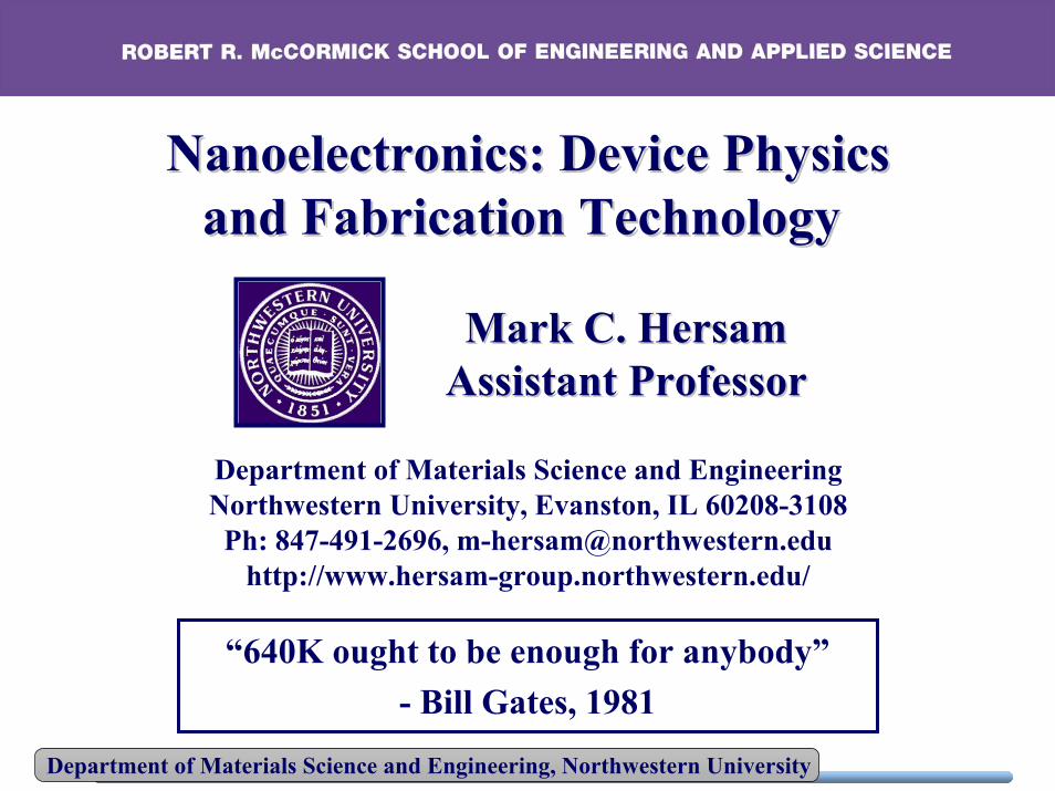
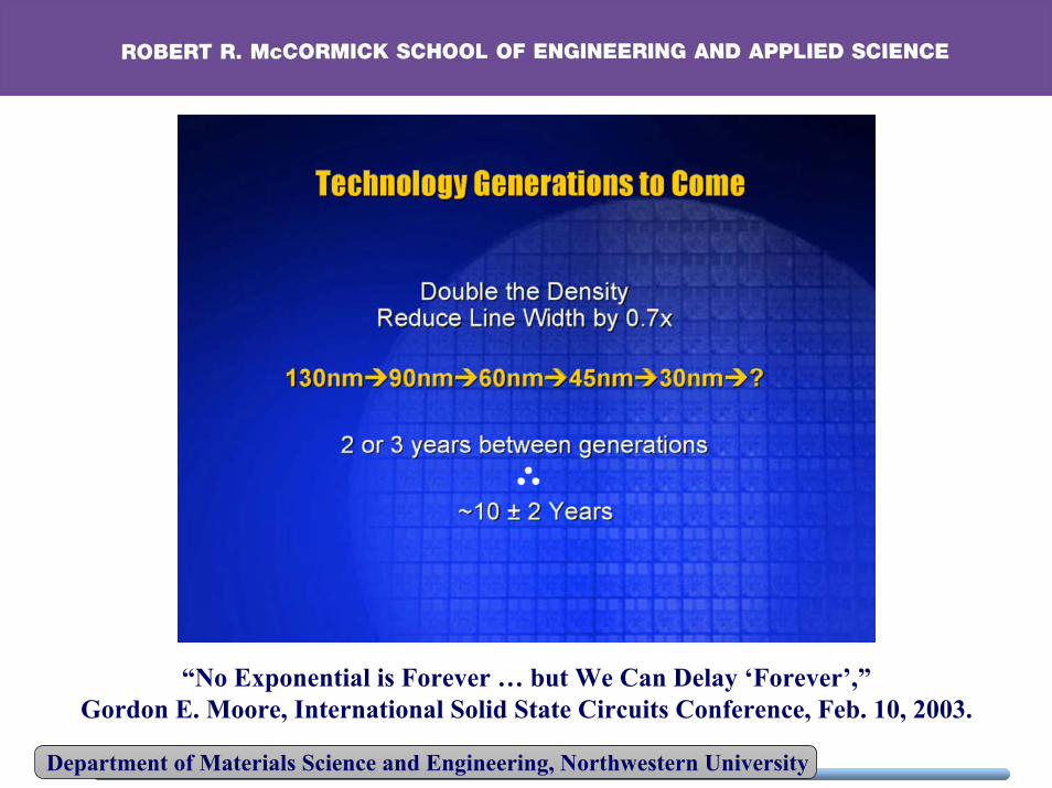
Moore’s Law
“Cramming More Components Onto Integrated Circuits”Author: Gordon E. Moore
Publication: Electronics, April 19, 1965
Intel Co-FounderGordon E. Moore
Department of Materials Science and Engineering, Northwestern University
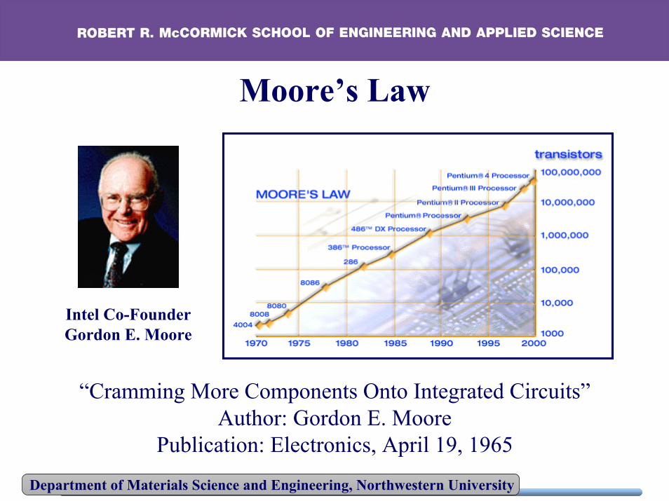
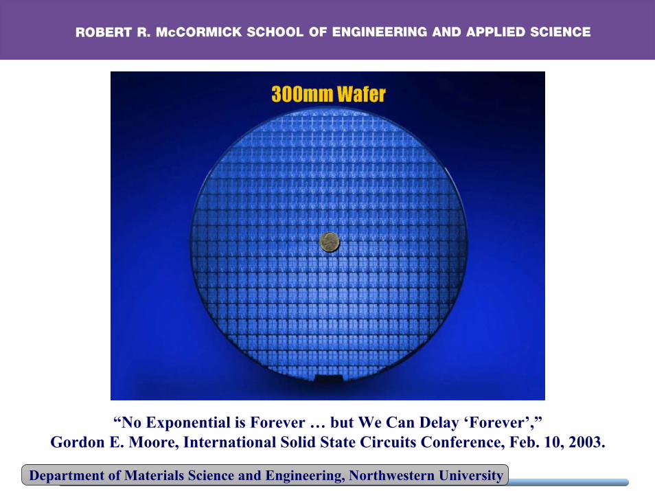
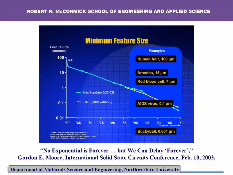
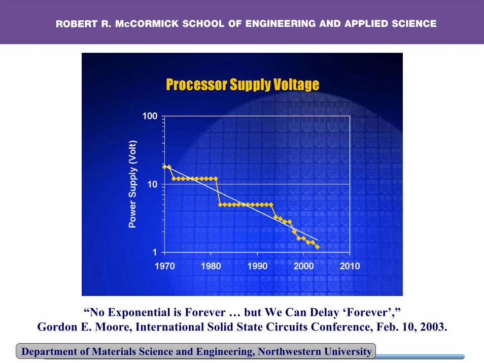
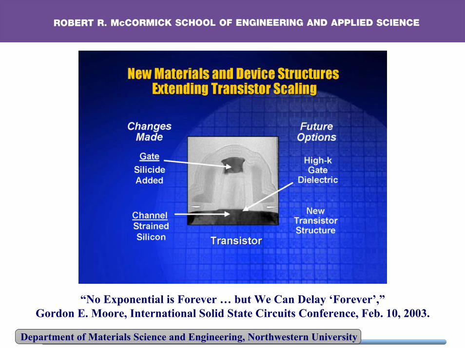
“No Exponential is Forever … but We Can Delay ‘Forever’,”Gordon E. Moore, International Solid State Circuits Conference, Feb. 10, 2003.
Department of Materials Science and Engineering, Northwestern University
“No Exponential is Forever … but We Can Delay ‘Forever’,”Gordon E. Moore, International Solid State Circuits Conference, Feb. 10, 2003.
Department of Materials Science and Engineering, Northwestern University
“No Exponential is Forever … but We Can Delay ‘Forever’,”Gordon E. Moore, International Solid State Circuits Conference, Feb. 10, 2003.
Department of Materials Science and Engineering, Northwestern University
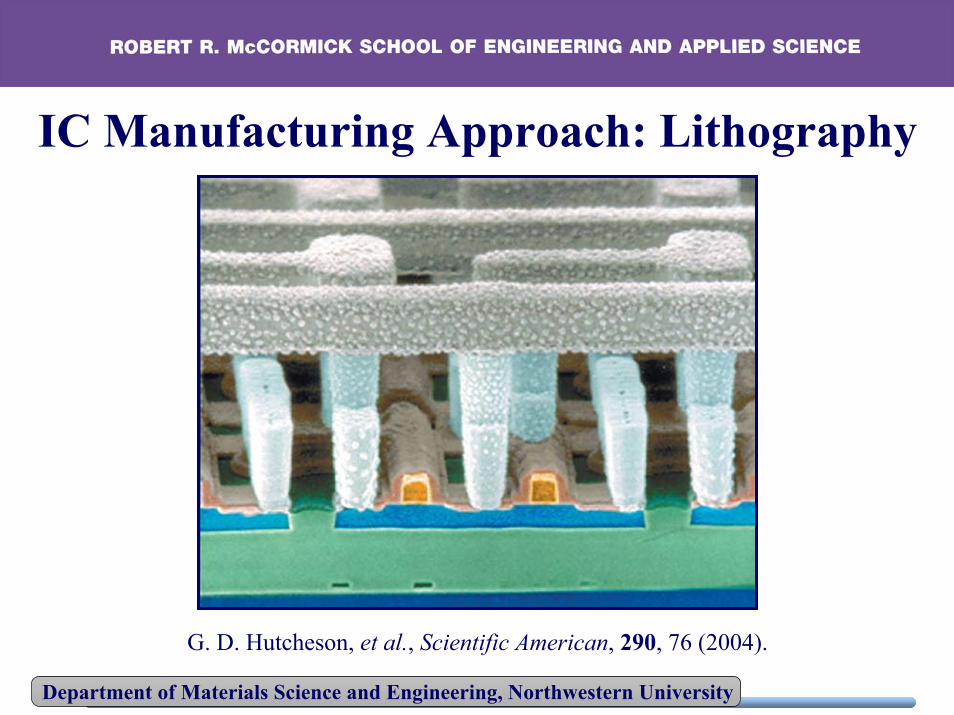
IC Manufacturing Approach: Lithography
G. D. Hutcheson, et al., Scientific American, 290, 76 (2004).
Department of Materials Science and Engineering, Northwestern University
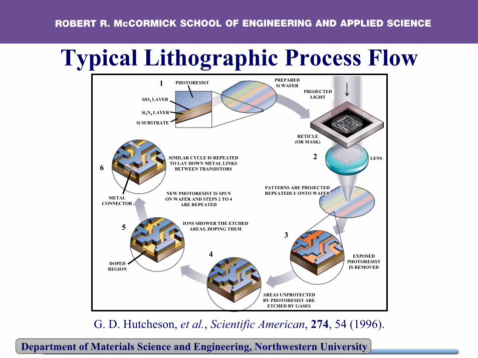
PHOTORESIST
SiO2 LAYER
Si3N4 LAYER
Si SUBSTRATE
1 PREPAREDSi WAFER
PROJECTEDLIGHT
RETICLE(OR MASK)
2
3
LENS
PATTERNS ARE PROJECTEDREPEATEDLY ONTO WAFER
EXPOSEDPHOTORESISTIS REMOVED
AREAS UNPROTECTEDBY PHOTORESIST ARE
ETCHED BY GASES
4
5
6
DOPEDREGION
IONS SHOWER THE ETCHEDAREAS, DOPING THEM
METALCONNECTOR
NEW PHOTORESIST IS SPUNON WAFER AND STEPS 2 TO 4
ARE REPEATED
SIMILAR CYCLE IS REPEATEDTO LAY DOWN METAL LINKS
BETWEEN TRANSISTORS
G. D. Hutcheson, et al., Scientific American, 274, 54 (1996).
Typical Lithographic Process Flow
Department of Materials Science and Engineering, Northwestern University
Lithography Yield
NOTE: Typical fabrication facilities (fabs) have product yields > 95%Lithography yield per step > 99%
Lithography is 90% of the production cost in modern day fabs
G. Timp, Nanotechnology, Chapter 4

Department of Materials Science and Engineering, Northwestern University
Lithography Areal Throughput
PhenomenologicalRelationship:
Resolution (Å) ~ 23At0.2
(At = areal throughput in μm2/hr)
This phenomenological relationship is essentially true over 18 orders of magnitude
in throughput!
G. Timp, Nanotechnology, Chapter 4
Department of Materials Science and Engineering, Northwestern University
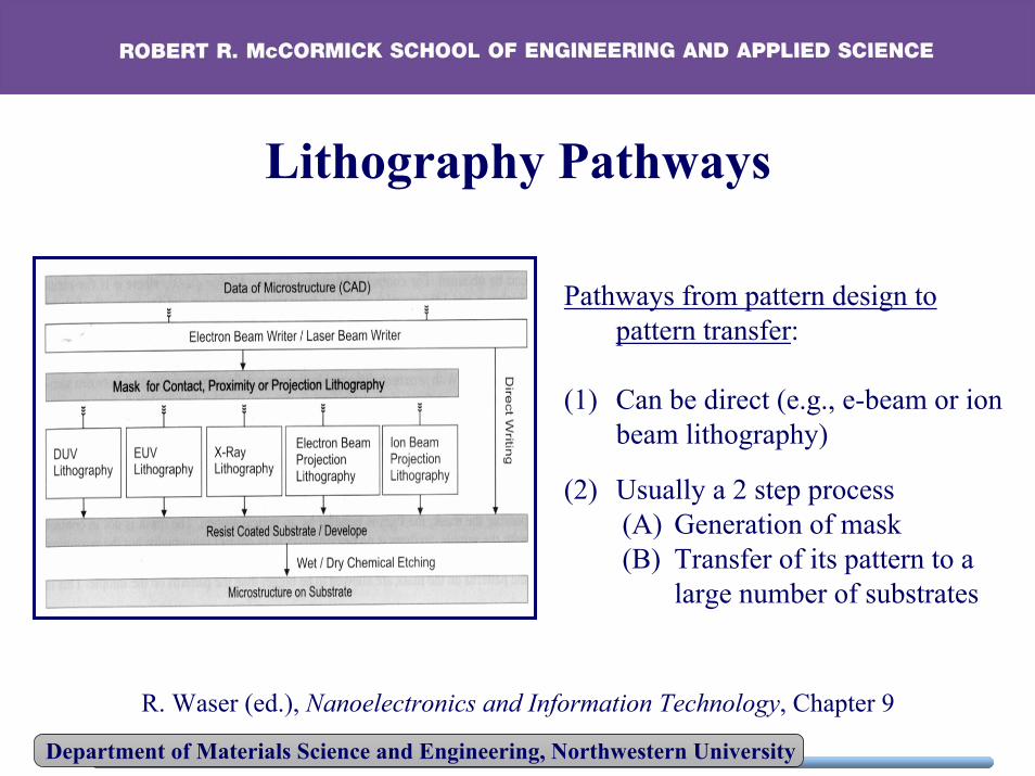
Lithography Pathways
Pathways from pattern design to pattern transfer:
(1) Can be direct (e.g., e-beam or ion beam lithography)
(2) Usually a 2 step process(A) Generation of mask(B) Transfer of its pattern to a
large number of substrates
R. Waser (ed.), Nanoelectronics and Information Technology, Chapter 9

Department of Materials Science and Engineering, Northwestern University
Masking Methods
Contact Proximity Projection
R. Waser (ed.), Nanoelectronics and Information Technology, Chapter 9
Department of Materials Science and Engineering, Northwestern University
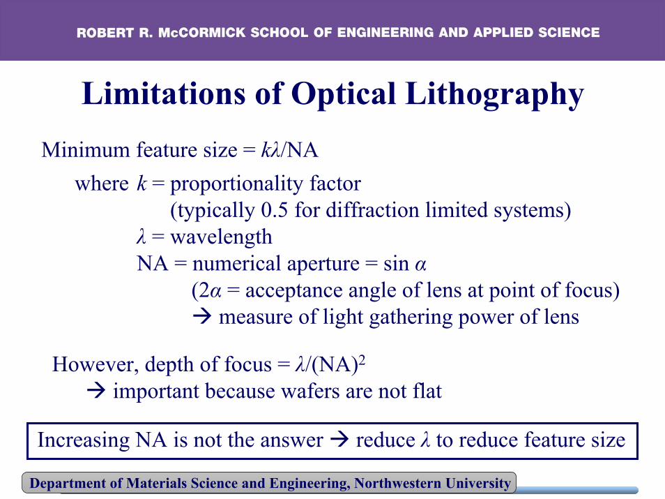
Limitations of Optical LithographyMinimum feature size = kλ/NA
where k = proportionality factor(typically 0.5 for diffraction limited systems)
λ = wavelengthNA = numerical aperture = sin α
(2α = acceptance angle of lens at point of focus)measure of light gathering power of lens
However, depth of focus = λ/(NA)2
important because wafers are not flat
Increasing NA is not the answer reduce λ to reduce feature size
Department of Materials Science and Engineering, Northwestern University
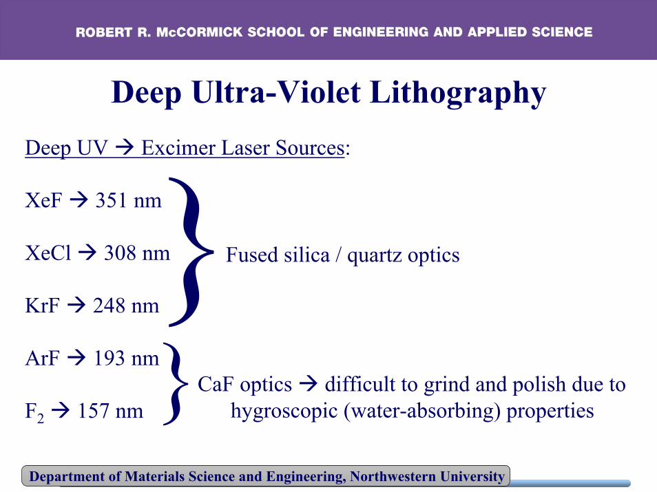
Deep Ultra-Violet LithographyDeep UV Excimer Laser Sources:
XeF 351 nm
XeCl 308 nm
KrF 248 nm
ArF 193 nm
F2 157 nm
Fused silica / quartz optics
}CaF optics difficult to grind and polish due to hygroscopic (water-absorbing) properties
Department of Materials Science and Engineering, Northwestern University
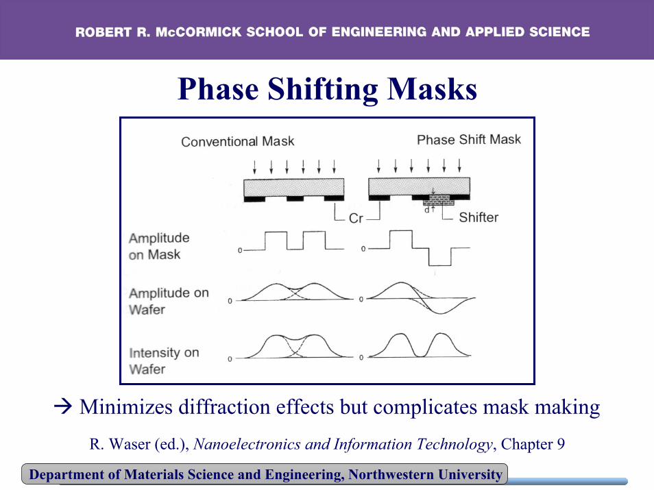
Phase Shifting Masks
Minimizes diffraction effects but complicates mask makingR. Waser (ed.), Nanoelectronics and Information Technology, Chapter 9
Department of Materials Science and Engineering, Northwestern University
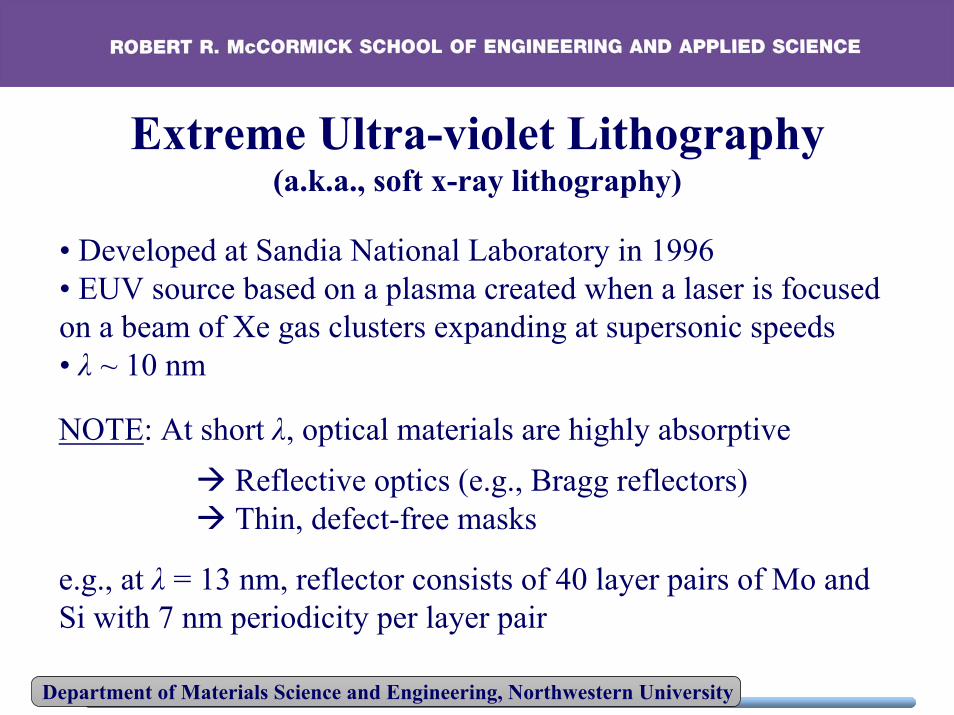
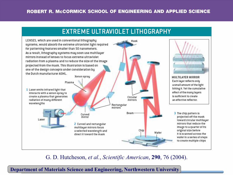
Extreme Ultra-violet Lithography(a.k.a., soft x-ray lithography)
• Developed at Sandia National Laboratory in 1996• EUV source based on a plasma created when a laser is focused on a beam of Xe gas clusters expanding at supersonic speeds• λ ~ 10 nm
NOTE: At short λ, optical materials are highly absorptiveReflective optics (e.g., Bragg reflectors)Thin, defect-free masks
e.g., at λ = 13 nm, reflector consists of 40 layer pairs of Mo and Si with 7 nm periodicity per layer pair
Department of Materials Science and Engineering, Northwestern University
G. D. Hutcheson, et al., Scientific American, 290, 76 (2004).
Department of Materials Science and Engineering, Northwestern University
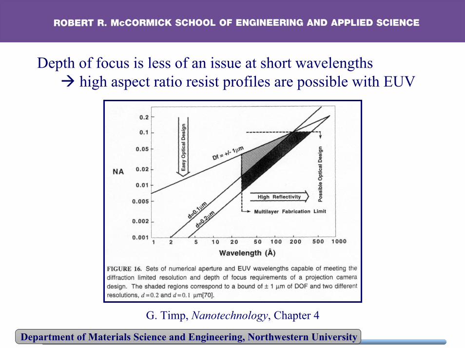
Depth of focus is less of an issue at short wavelengthshigh aspect ratio resist profiles are possible with EUV
G. Timp, Nanotechnology, Chapter 4
Department of Materials Science and Engineering, Northwestern University
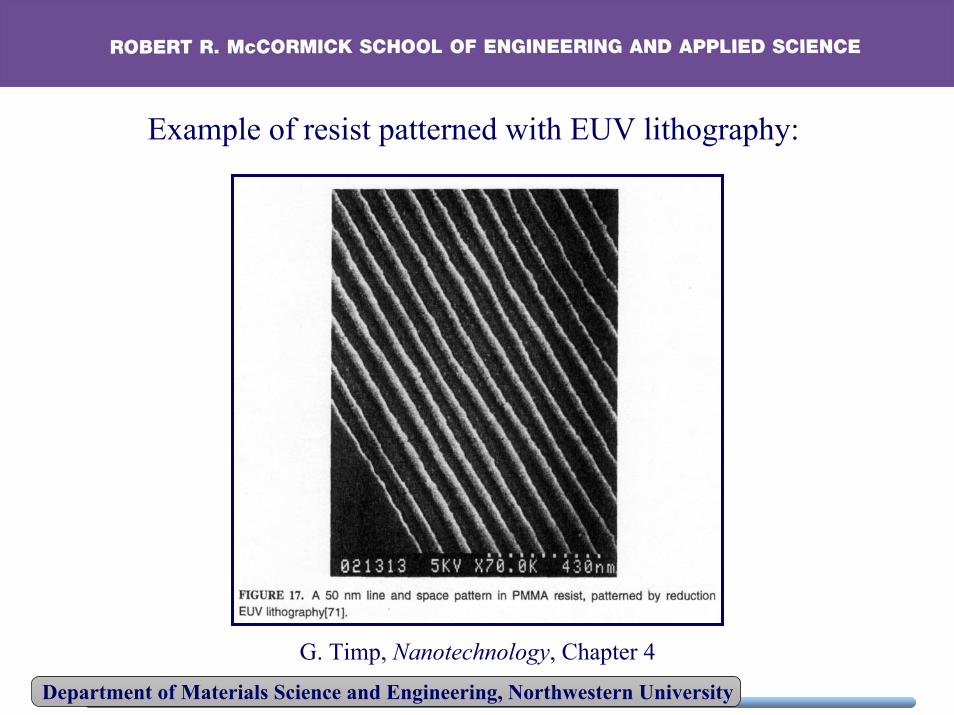
Example of resist patterned with EUV lithography:
G. Timp, Nanotechnology, Chapter 4
Department of Materials Science and Engineering, Northwestern University
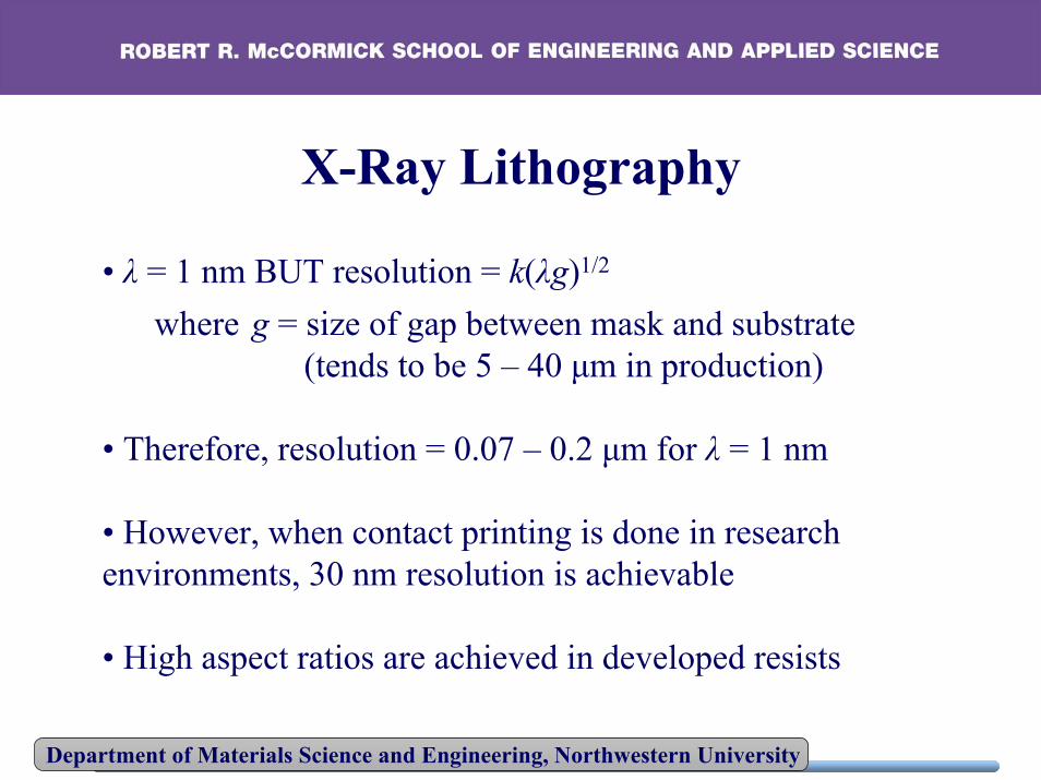
X-Ray Lithography
• λ = 1 nm BUT resolution = k(λg)1/2
where g = size of gap between mask and substrate(tends to be 5 – 40 μm in production)
• Therefore, resolution = 0.07 – 0.2 μm for λ = 1 nm
• However, when contact printing is done in research environments, 30 nm resolution is achievable
• High aspect ratios are achieved in developed resists
Department of Materials Science and Engineering, Northwestern University
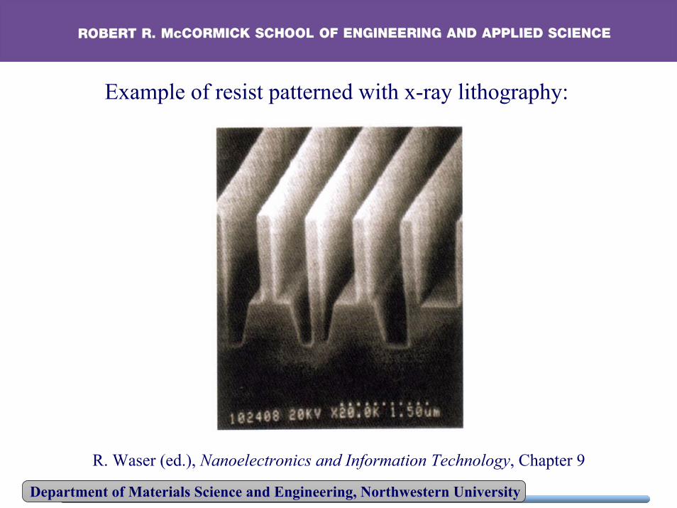
Example of resist patterned with x-ray lithography:
R. Waser (ed.), Nanoelectronics and Information Technology, Chapter 9
Department of Materials Science and Engineering, Northwestern University
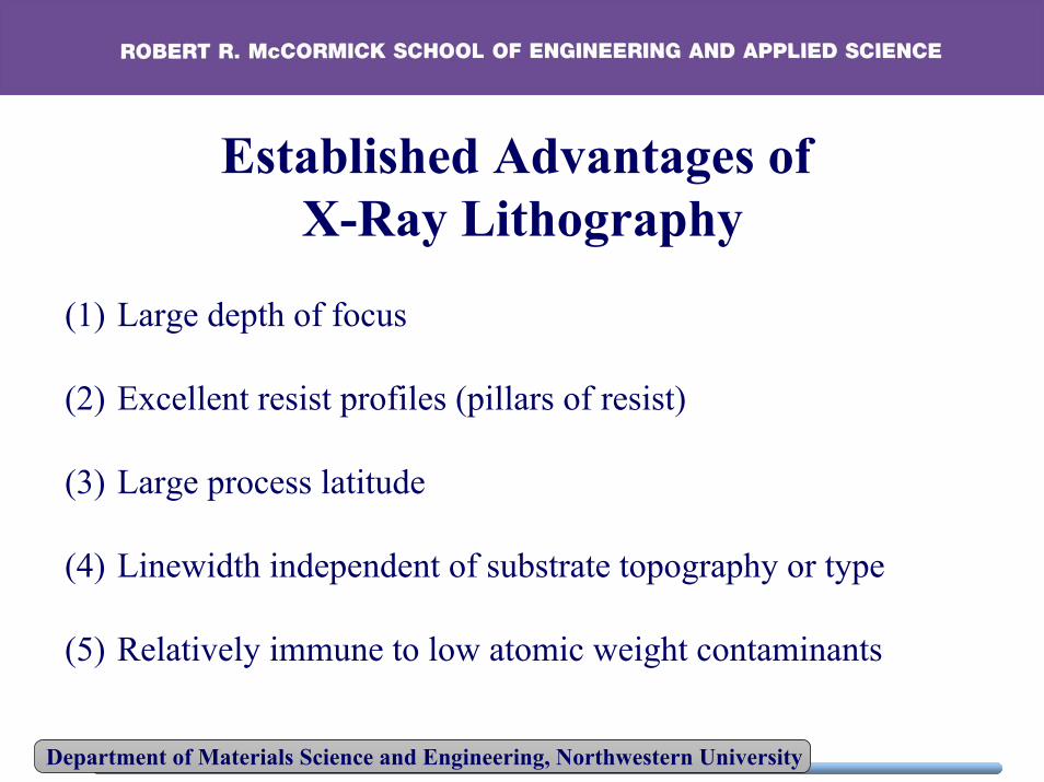
Established Advantages of X-Ray Lithography
(1) Large depth of focus
(2) Excellent resist profiles (pillars of resist)
(3) Large process latitude
(4) Linewidth independent of substrate topography or type
(5) Relatively immune to low atomic weight contaminants
Department of Materials Science and Engineering, Northwestern University
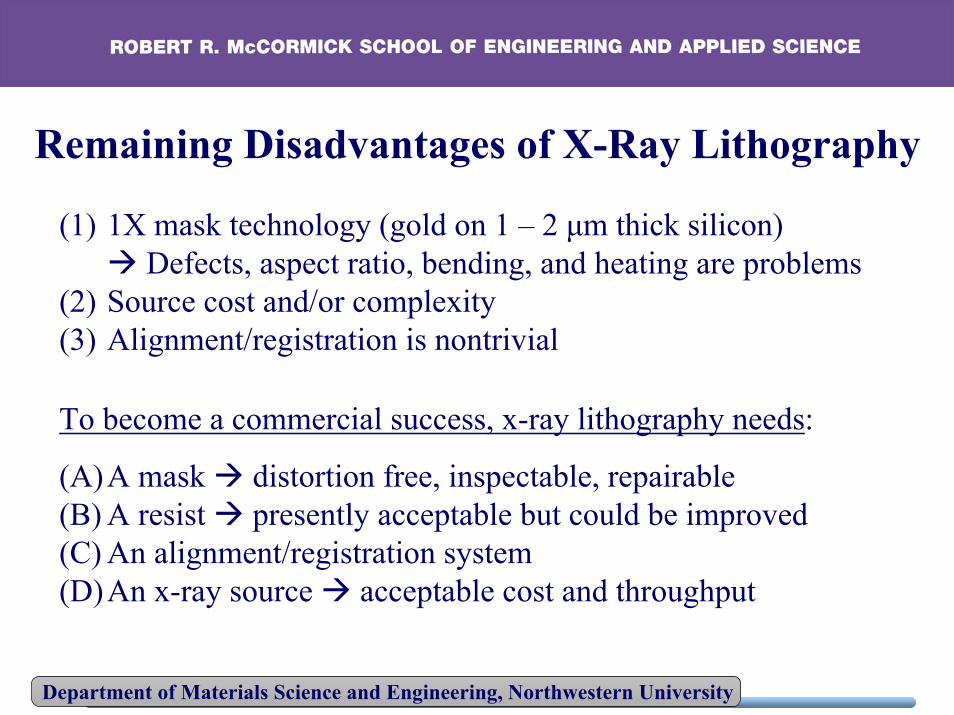
Remaining Disadvantages of X-Ray Lithography
(1) 1X mask technology (gold on 1 – 2 μm thick silicon)Defects, aspect ratio, bending, and heating are problems
(2) Source cost and/or complexity(3) Alignment/registration is nontrivial
To become a commercial success, x-ray lithography needs:
(A)A mask distortion free, inspectable, repairable(B) A resist presently acceptable but could be improved(C) An alignment/registration system(D)An x-ray source acceptable cost and throughput
Department of Materials Science and Engineering, Northwestern University
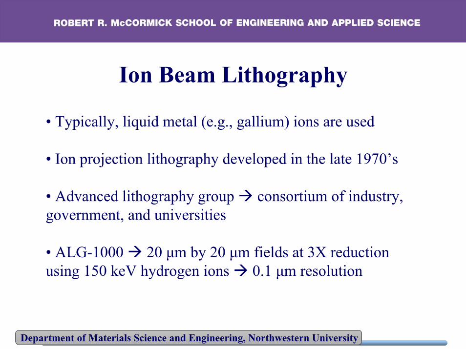
Ion Beam Lithography
• Typically, liquid metal (e.g., gallium) ions are used
• Ion projection lithography developed in the late 1970’s
• Advanced lithography group consortium of industry, government, and universities
• ALG-1000 20 μm by 20 μm fields at 3X reduction using 150 keV hydrogen ions 0.1 μm resolution
Department of Materials Science and Engineering, Northwestern University
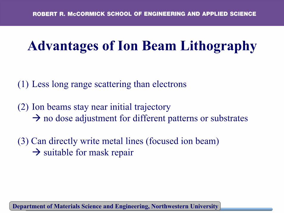
Advantages of Ion Beam Lithography
(1) Less long range scattering than electrons
(2) Ion beams stay near initial trajectoryno dose adjustment for different patterns or substrates
(3) Can directly write metal lines (focused ion beam)suitable for mask repair

Department of Materials Science and Engineering, Northwestern University
Disadvantages of Ion Beam Lithography(1) Ions interact strongly with target causing:
(A)Ion mixing(B) Amorphizing crystals(C) Altered optical properties(D)Implanted dopants(E) Sputter etching
(2) Ions are highly absorbed (typically within 10 nm)Stencil type masksThe center of a ring falls out unless sub-resolution
supports are used
Department of Materials Science and Engineering, Northwestern University
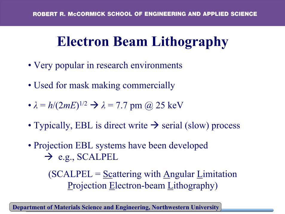
Electron Beam Lithography• Very popular in research environments
• Used for mask making commercially
• λ = h/(2mE)1/2 λ = 7.7 pm @ 25 keV
• Typically, EBL is direct write serial (slow) process
• Projection EBL systems have been developede.g., SCALPEL
(SCALPEL = Scattering with Angular Limitation Projection Electron-beam Lithography)
Department of Materials Science and Engineering, Northwestern University
Advantages of Electron Beam Lithography
(1) High resolution down to 5 nm(2) Useful design tool direct write allows for quick pattern
changes (no masks are needed)
Disadvantages of Electron Beam Lithography
(1) Cost (up to $6 – 10 million for hardware)(2) Direct write has low throughput slow and expensive
Department of Materials Science and Engineering, Northwestern University
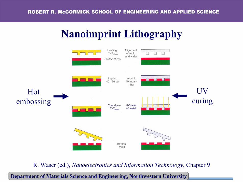
Nanoimprint Lithography
Hotembossing
UVcuring
R. Waser (ed.), Nanoelectronics and Information Technology, Chapter 9
Department of Materials Science and Engineering, Northwestern University
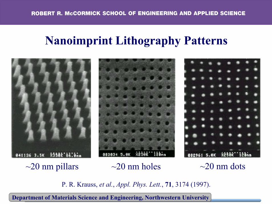
P. R. Krauss, et al., Appl. Phys. Lett., 71, 3174 (1997).
~20 nm pillars ~20 nm holes ~20 nm dots
Nanoimprint Lithography Patterns

Department of Materials Science and Engineering, Northwestern University
p-Si
SiO2 SiO2n-n- n+n+
Silicon MOSFET Geometry
MOSFET = Metal-Oxide-Semiconductor Field Effect Transistor
Department of Materials Science and Engineering, Northwestern University
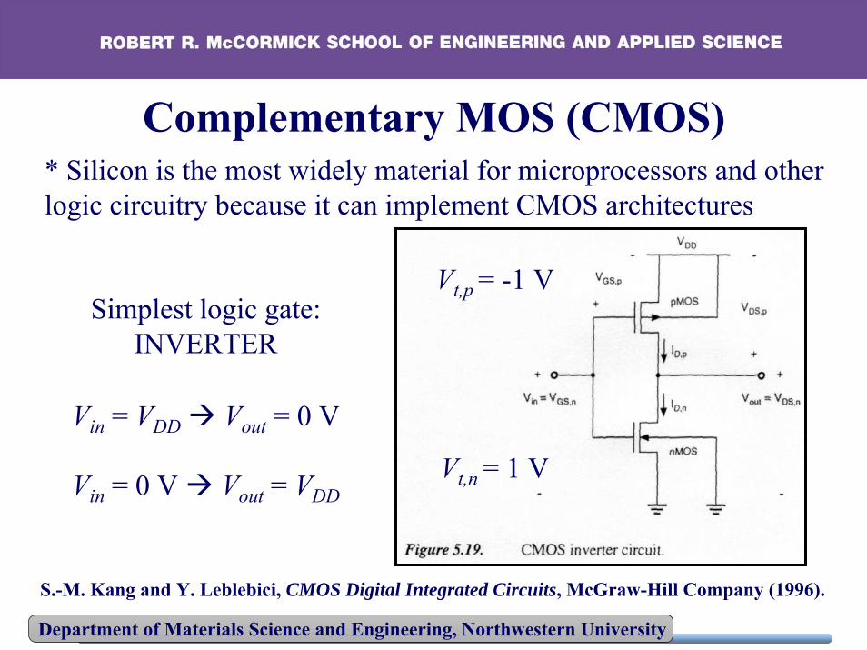
Complementary MOS (CMOS)* Silicon is the most widely material for microprocessors and otherlogic circuitry because it can implement CMOS architectures
Simplest logic gate:INVERTER
Vin = VDD Vout = 0 V
Vin = 0 V Vout = VDD
Vt,p = -1 V
Vt,n = 1 V
S.-M. Kang and Y. Leblebici, CMOS Digital Integrated Circuits, McGraw-Hill Company (1996).
Department of Materials Science and Engineering, Northwestern University
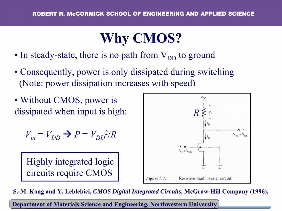
Why CMOS?• In steady-state, there is no path from VDD to ground
• Consequently, power is only dissipated during switching(Note: power dissipation increases with speed)
• Without CMOS, power isdissipated when input is high:
Vin = VDD P = VDD2/R
R
Highly integrated logiccircuits require CMOS
S.-M. Kang and Y. Leblebici, CMOS Digital Integrated Circuits, McGraw-Hill Company (1996).
Department of Materials Science and Engineering, Northwestern University
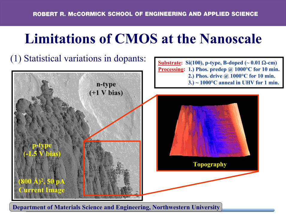
Limitations of CMOS at the Nanoscale(1) Statistical variations in dopants: Substrate: Si(100), p-type, B-doped (~ 0.01 Ω-cm)
Processing: 1.) Phos. predep @ 1000°C for 10 min.2.) Phos. drive @ 1000°C for 10 min.3.) ~ 1000°C anneal in UHV for 1 min.
p-type(-1.5 V bias)
(800 Å)2, 50 pACurrent Image
n-type(+1 V bias)
Topography
Department of Materials Science and Engineering, Northwestern University
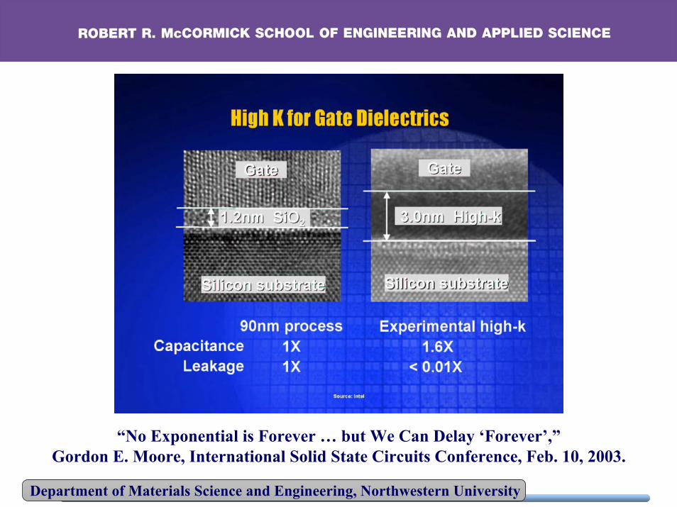
Limitations of CMOS at the Nanoscale(2) Gate oxide scales with channel length
(At ~ 1 nm gate oxide thickness, large gate leakage currentdue to tunneling)
NOTE: Cox = εoxA/dox
(Rather than decrease dox, increase εox)
High k dielectric materials
Department of Materials Science and Engineering, Northwestern University
“No Exponential is Forever … but We Can Delay ‘Forever’,”Gordon E. Moore, International Solid State Circuits Conference, Feb. 10, 2003.
Department of Materials Science and Engineering, Northwestern University
Problems with High K DielectricsTwo new interfaces:
(1) Interface between high k dielectric and silicon needsto be as free of dangling bonds as possible
(2) Interface between high k dielectric and poly silicon gateleads to two problems:
(a) Phonon scattering, which decreases speed
(b) Threshold voltage is pinned to high values
Department of Materials Science and Engineering, Northwestern University
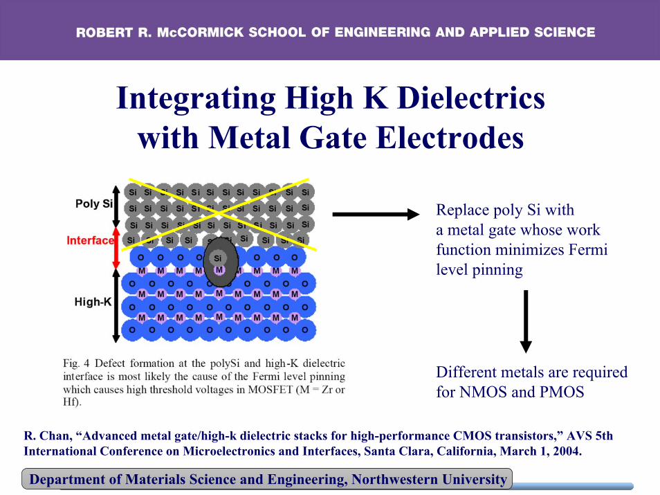
Integrating High K Dielectricswith Metal Gate Electrodes
Replace poly Si witha metal gate whose work function minimizes Fermi level pinning
Different metals are required for NMOS and PMOS
R. Chan, “Advanced metal gate/high-k dielectric stacks for high-performance CMOS transistors,” AVS 5th International Conference on Microelectronics and Interfaces, Santa Clara, California, March 1, 2004.
Department of Materials Science and Engineering, Northwestern University
Limitations of CMOS at the Nanoscale
(3) Interconnects scale with channel length
Higher J = I/A, R = ρl/A
electromigration and other failure mechanisms
electromigration concerns motivated the switchfrom aluminum to copper interconnects

Department of Materials Science and Engineering, Northwestern University
Potentiometry of Nanowire Failure
B
Onset offailure
0.8V 1V C
Failurepoint
0.9V 1.8V
(Breakdown current density = 3.75×10¹² A/m2).
Contact mode AFM potentiometry images: Wire width = 60 nm
0.8V 1VA
Evolution of nanowire failure:
M. C. Hersam, A. C. F. Hoole, S. J. O'Shea, and M. E. Welland, Appl. Phys. Lett., 72, 915 (1998).
Department of Materials Science and Engineering, Northwestern University
Limitations of CMOS at the Nanoscale
(4) Hot electron effects
As channel length decreases, E-field increases (E = V/l)
“Hot electrons” desorb hydrogen at interface(replace with deuterium to increase lifetime)
Alternatively, decrease V implies tighter control ofnoise and device characteristics
Department of Materials Science and Engineering, Northwestern University
“No Exponential is Forever … but We Can Delay ‘Forever’,”Gordon E. Moore, International Solid State Circuits Conference, Feb. 10, 2003.
Department of Materials Science and Engineering, Northwestern University
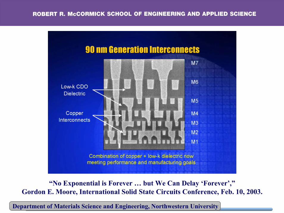
Limitations of CMOS at the Nanoscale
(5) Interconnect cross-talk
Capacitive coupling increases as spacing between interconnects decreases (C = εA/d)
To decrease d, ε needs to be decreased
Low-k dielectric materials (porous materials)
Department of Materials Science and Engineering, Northwestern University
“No Exponential is Forever … but We Can Delay ‘Forever’,”Gordon E. Moore, International Solid State Circuits Conference, Feb. 10, 2003.
Department of Materials Science and Engineering, Northwestern University
(6) Power Dissipation
Although CMOS ideally has no steady state powerdissipation, power is dissipated during switching.
As clock speed and device densities increase, power dissipation increases
Steady state leakage power is also increasing due to gateleakage current and leakage to substrate
Gate leakage is minimized with high k dielectrics;substrate leakage is minimized with silicon-on-insulator
Limitations of CMOS at the Nanoscale

Department of Materials Science and Engineering, Northwestern University
“No Exponential is Forever … but We Can Delay ‘Forever’,”Gordon E. Moore, International Solid State Circuits Conference, Feb. 10, 2003.
Department of Materials Science and Engineering, Northwestern University
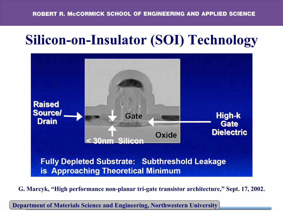
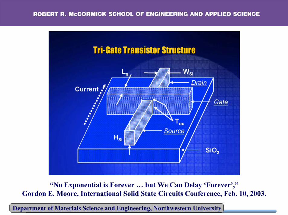
Silicon-on-Insulator (SOI) Technology
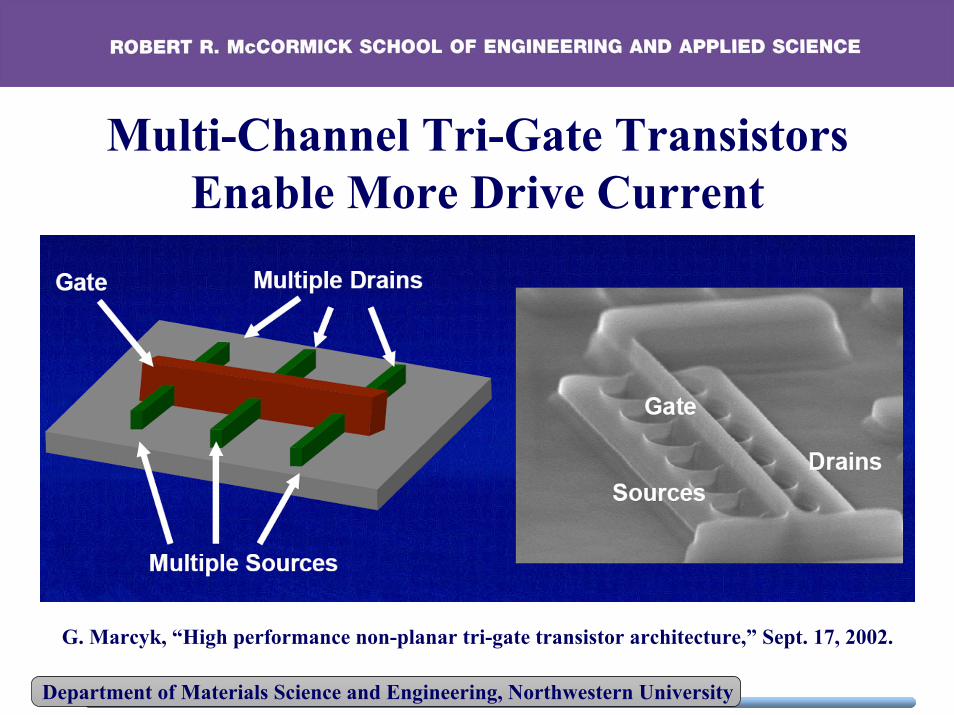
G. Marcyk, “High performance non-planar tri-gate transistor architecture,” Sept. 17, 2002.
Department of Materials Science and Engineering, Northwestern University
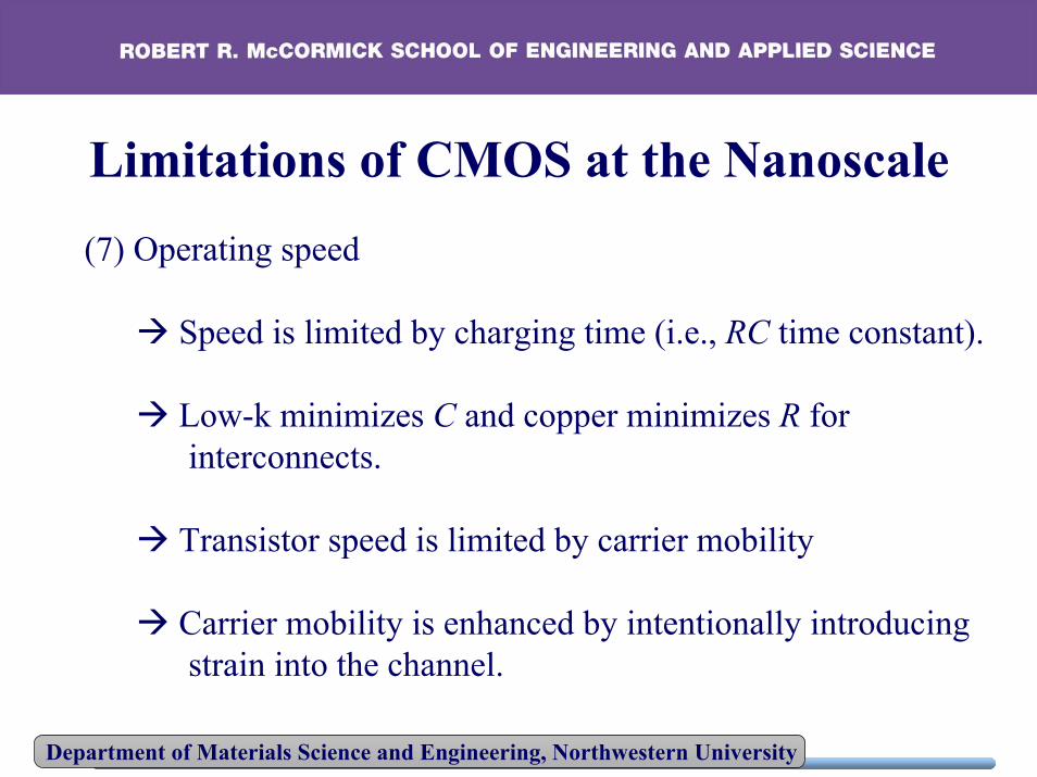
(7) Operating speed
Speed is limited by charging time (i.e., RC time constant).
Low-k minimizes C and copper minimizes R forinterconnects.
Transistor speed is limited by carrier mobility
Carrier mobility is enhanced by intentionally introducing strain into the channel.
Limitations of CMOS at the Nanoscale
Department of Materials Science and Engineering, Northwestern University
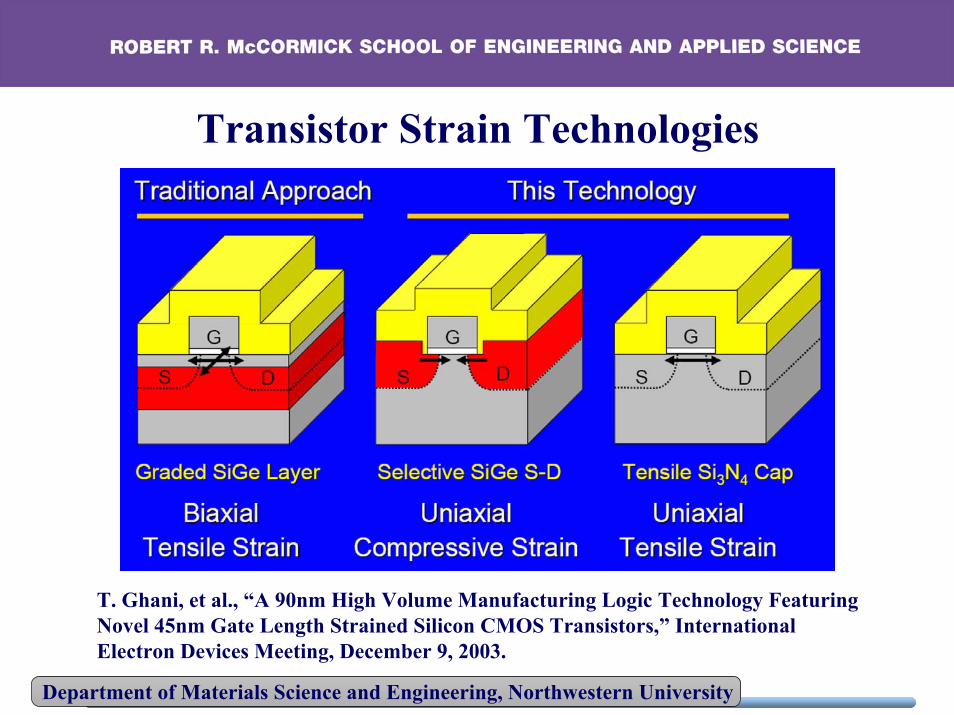
T. Ghani, et al., “A 90nm High Volume Manufacturing Logic Technology Featuring Novel 45nm Gate Length Strained Silicon CMOS Transistors,” International Electron Devices Meeting, December 9, 2003.
Transistor Strain Technologies
Department of Materials Science and Engineering, Northwestern University
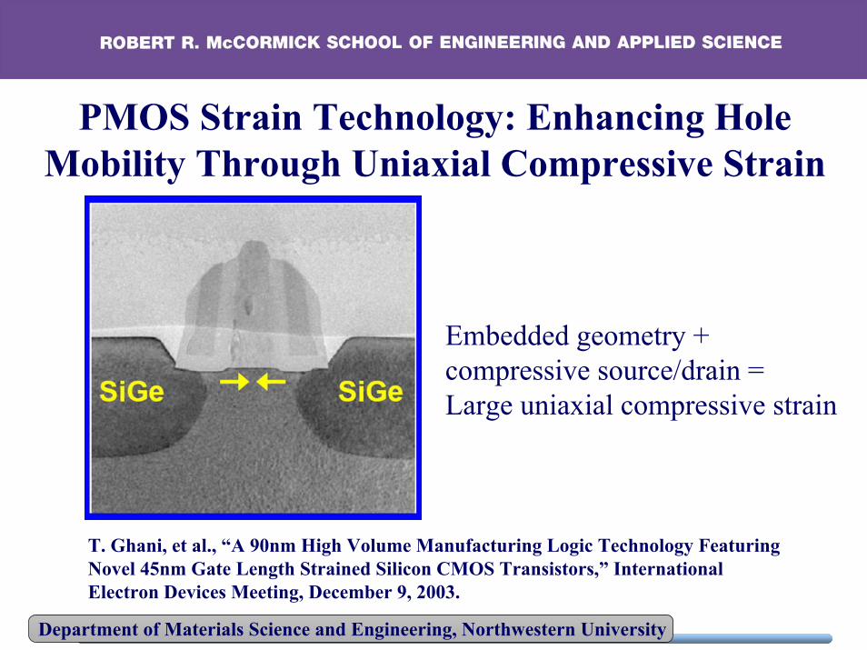
PMOS Strain Technology: Enhancing HoleMobility Through Uniaxial Compressive Strain
T. Ghani, et al., “A 90nm High Volume Manufacturing Logic Technology Featuring Novel 45nm Gate Length Strained Silicon CMOS Transistors,” International Electron Devices Meeting, December 9, 2003.
Embedded geometry +compressive source/drain =Large uniaxial compressive strain
Department of Materials Science and Engineering, Northwestern University
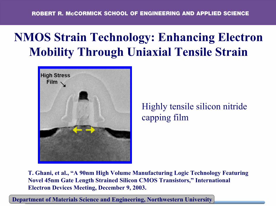
NMOS Strain Technology: Enhancing ElectronMobility Through Uniaxial Tensile Strain
T. Ghani, et al., “A 90nm High Volume Manufacturing Logic Technology Featuring Novel 45nm Gate Length Strained Silicon CMOS Transistors,” International Electron Devices Meeting, December 9, 2003.
Highly tensile silicon nitride capping film
Department of Materials Science and Engineering, Northwestern University
(8) Cost
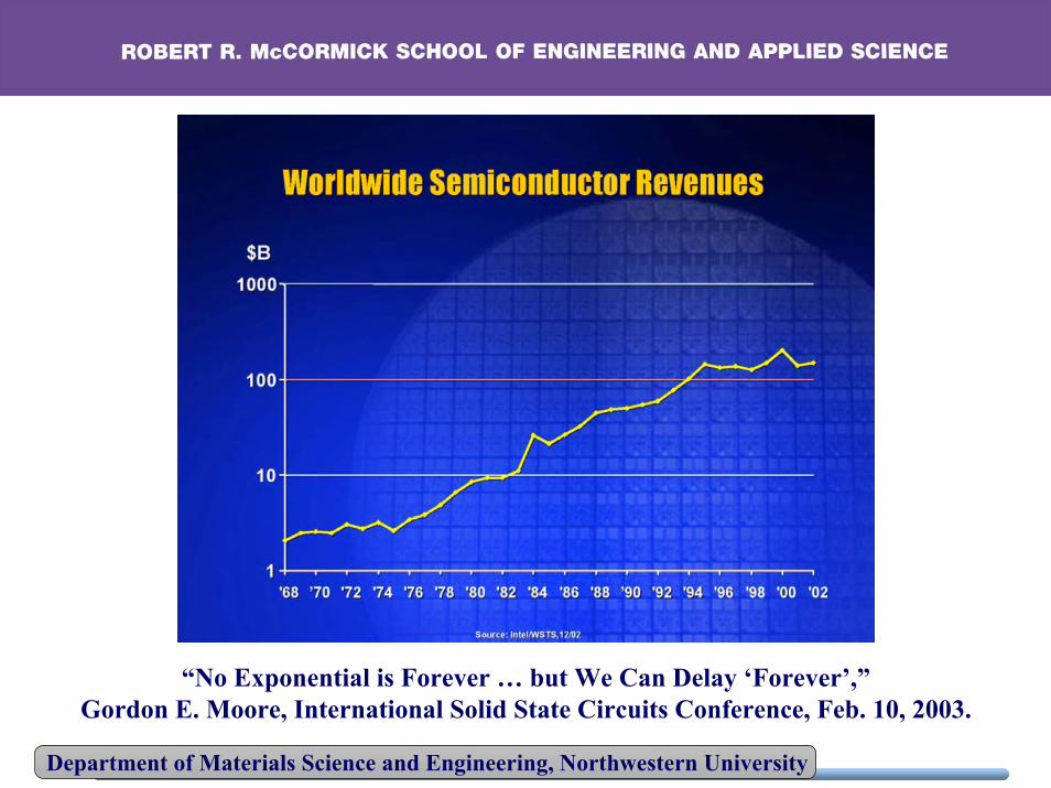
Revenues increase by ~16%/year
Factory cost increases by ~19%/year
Plus, advanced lithographies (e-beam, ion beam, X-ray, EUV)are currently more expensive than DUV lithography
Costs are expected to rise more quickly than revenues in the future
Limitations of CMOS at the Nanoscale
Department of Materials Science and Engineering, Northwestern University
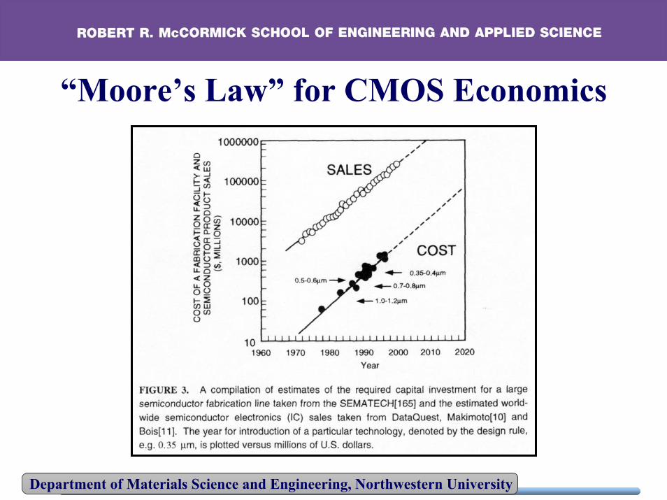
“Moore’s Law” for CMOS Economics
Department of Materials Science and Engineering, Northwestern University
“No Exponential is Forever … but We Can Delay ‘Forever’,”Gordon E. Moore, International Solid State Circuits Conference, Feb. 10, 2003.

Department of Materials Science and Engineering, Northwestern University
“No Exponential is Forever … but We Can Delay ‘Forever’,”Gordon E. Moore, International Solid State Circuits Conference, Feb. 10, 2003.
Department of Materials Science and Engineering, Northwestern University
“No Exponential is Forever … but We Can Delay ‘Forever’,”Gordon E. Moore, International Solid State Circuits Conference, Feb. 10, 2003.
Department of Materials Science and Engineering, Northwestern University
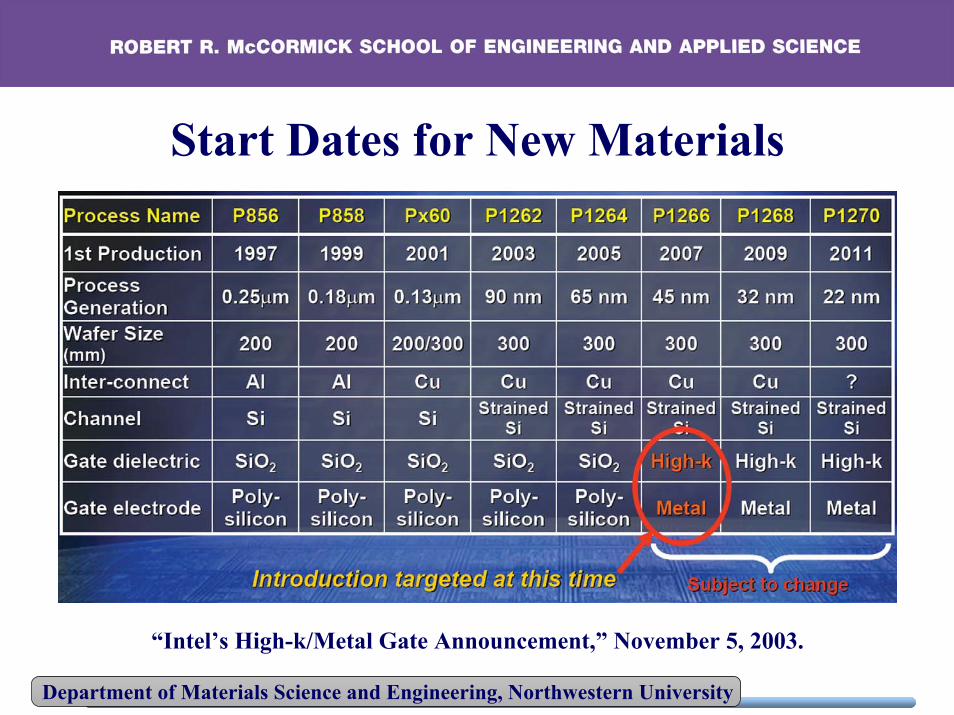
Start Dates for New Materials
“Intel’s High-k/Metal Gate Announcement,” November 5, 2003.
Department of Materials Science and Engineering, Northwestern University
“No Exponential is Forever … but We Can Delay ‘Forever’,”Gordon E. Moore, International Solid State Circuits Conference, Feb. 10, 2003.

Department of Materials Science and Engineering, Northwestern University
Fabricated Tri-Gate Transistor
G. Marcyk, “High performance non-planar tri-gate transistor architecture,” Sept. 17, 2002.
Department of Materials Science and Engineering, Northwestern University
G. Marcyk, “High performance non-planar tri-gate transistor architecture,” Sept. 17, 2002.
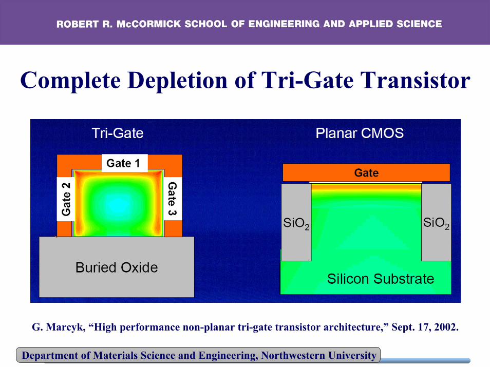
Complete Depletion of Tri-Gate Transistor
Department of Materials Science and Engineering, Northwestern University
G. Marcyk, “High performance non-planar tri-gate transistor architecture,” Sept. 17, 2002.
Multi-Channel Tri-Gate TransistorsEnable More Drive Current
Department of Materials Science and Engineering, Northwestern University
“No Exponential is Forever … but We Can Delay ‘Forever’,”Gordon E. Moore, International Solid State Circuits Conference, Feb. 10, 2003.
Department of Materials Science and Engineering, Northwestern University
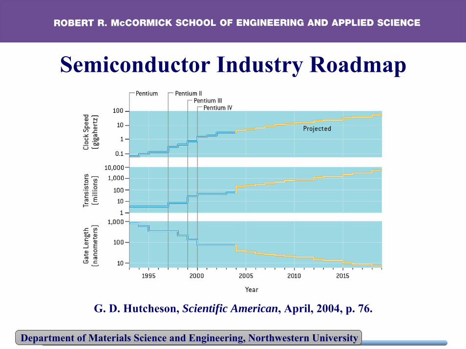
G. D. Hutcheson, Scientific American, April, 2004, p. 76.
Semiconductor Industry Roadmap
Department of Materials Science and Engineering, Northwestern University
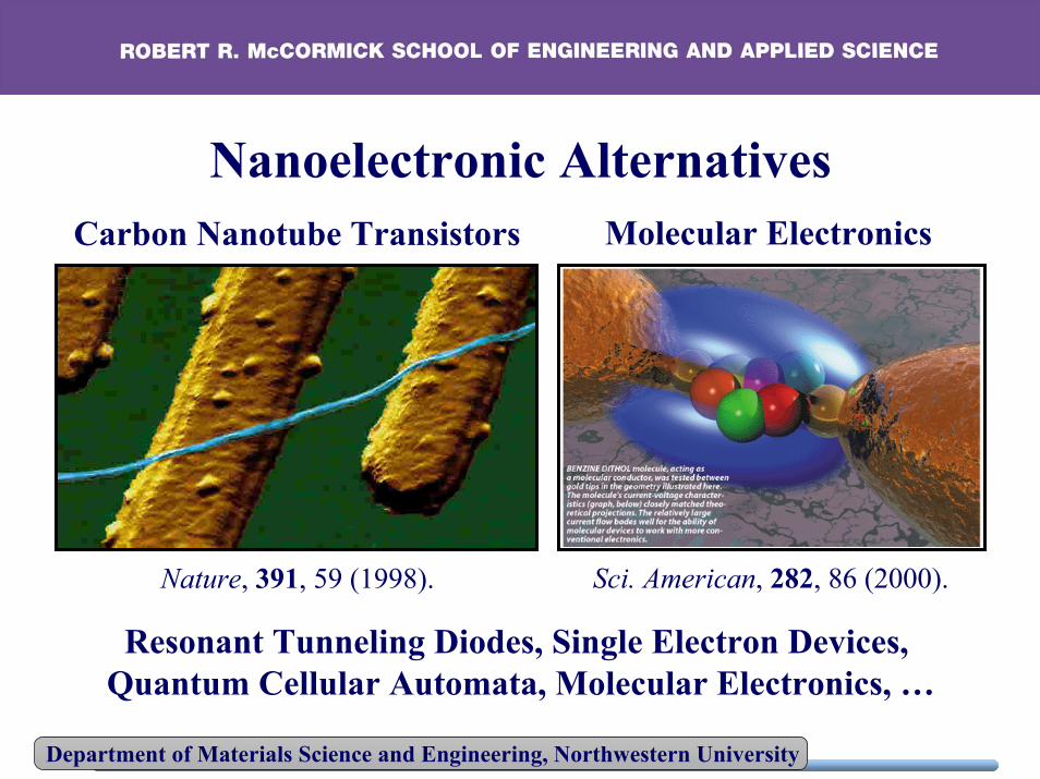
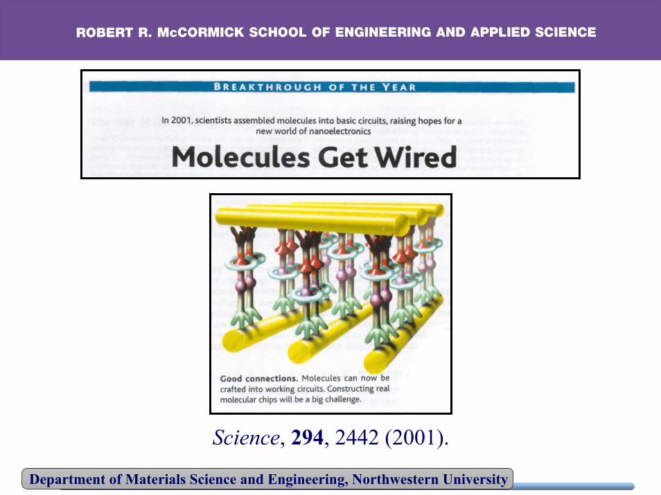
Nanoelectronic Alternatives
Resonant Tunneling Diodes, Single Electron Devices, Quantum Cellular Automata, Molecular Electronics, …
Nature, 391, 59 (1998).
Carbon Nanotube Transistors Molecular Electronics
Sci. American, 282, 86 (2000).
Department of Materials Science and Engineering, Northwestern University
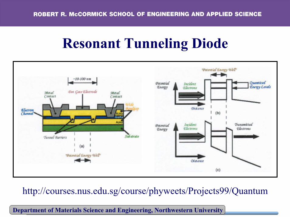
http://courses.nus.edu.sg/course/phyweets/Projects99/Quantum
Resonant Tunneling Diode
Department of Materials Science and Engineering, Northwestern University
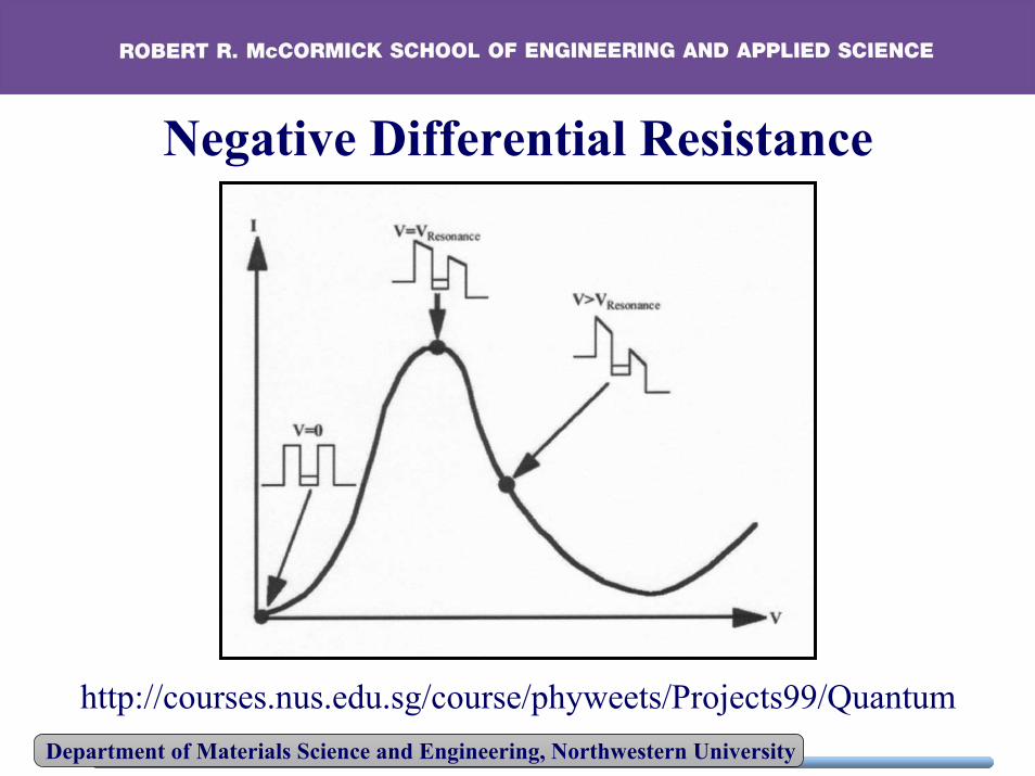
http://courses.nus.edu.sg/course/phyweets/Projects99/Quantum
Negative Differential Resistance
Department of Materials Science and Engineering, Northwestern University
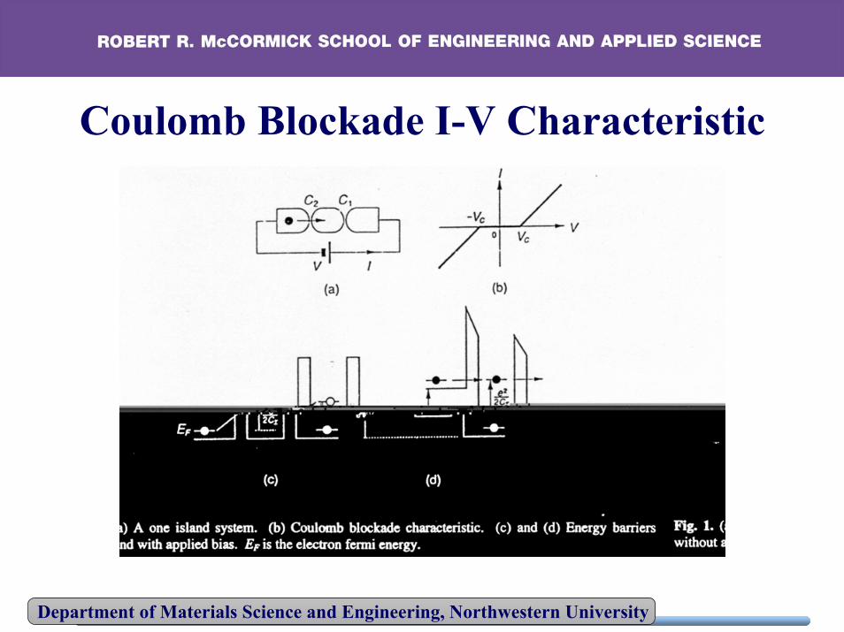
Single Electron DevicesCoulomb Blockade: Suppression of electron tunneling to an island(0-D quantum dot) by a single electron charging energy
NOTE: Capacitor charging energy = Q2/2CFor a single electron e2/2C
Two Conditions for Coulomb Blockade:
(1) Thermal Fluctuations: e2/C >> kT
(2) Heisenberg Uncertainty: ΔEΔt >> h(e2/C)(RtC) >> h Rt >> h/e2
Department of Materials Science and Engineering, Northwestern University
Temperature Requirement forCoulomb Blockade
Temperature Condition for Coulomb Blockade:
To suppress thermal fluctuations, e2/C >> kT
For room temperature operation, C ~ 1 aF = 10-18 F
For C ~ 1 aF, quantum dot dimensions ~ 1 nm
Since it is challenging to fabricate down to 1 nm, mostsingle electron devices only operate at low temperature
Department of Materials Science and Engineering, Northwestern University
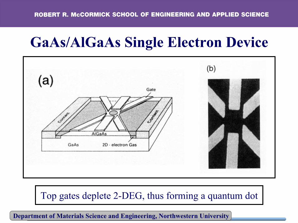
GaAs/AlGaAs Single Electron Device
Top gates deplete 2-DEG, thus forming a quantum dot
Department of Materials Science and Engineering, Northwestern University
Coulomb Blockade I-V Characteristic
Department of Materials Science and Engineering, Northwestern University
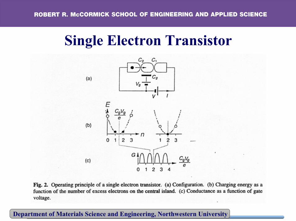
Single Electron Transistor
Department of Materials Science and Engineering, Northwestern University
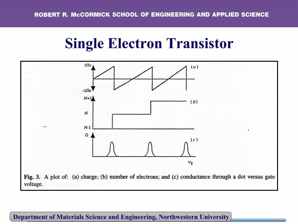
Single Electron Transistor
Department of Materials Science and Engineering, Northwestern University
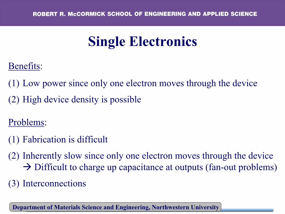
Single ElectronicsBenefits:
(1) Low power since only one electron moves through the device
(2) High device density is possible
Problems:
(1) Fabrication is difficult
(2) Inherently slow since only one electron moves through the deviceDifficult to charge up capacitance at outputs (fan-out problems)
(3) Interconnections
Department of Materials Science and Engineering, Northwestern University
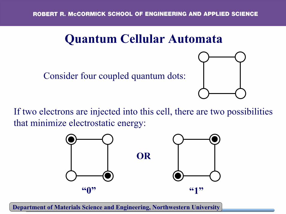
Quantum Cellular Automata
Consider four coupled quantum dots:
If two electrons are injected into this cell, there are two possibilitiesthat minimize electrostatic energy:
OR
“0” “1”
Department of Materials Science and Engineering, Northwestern University
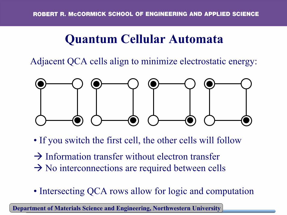
Quantum Cellular Automata
Adjacent QCA cells align to minimize electrostatic energy:
• If you switch the first cell, the other cells will follow
Information transfer without electron transferNo interconnections are required between cells
• Intersecting QCA rows allow for logic and computation
Department of Materials Science and Engineering, Northwestern University
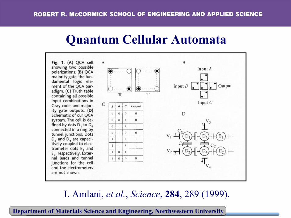
Quantum Cellular Automata
I. Amlani, et al., Science, 284, 289 (1999).
Department of Materials Science and Engineering, Northwestern University
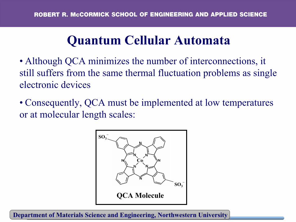
Quantum Cellular Automata• Although QCA minimizes the number of interconnections, itstill suffers from the same thermal fluctuation problems as singleelectronic devices
• Consequently, QCA must be implemented at low temperaturesor at molecular length scales:
SO3–
SO3–
QCA Molecule
Co
Department of Materials Science and Engineering, Northwestern University
Science, 294, 2442 (2001).
Department of Materials Science and Engineering, Northwestern University
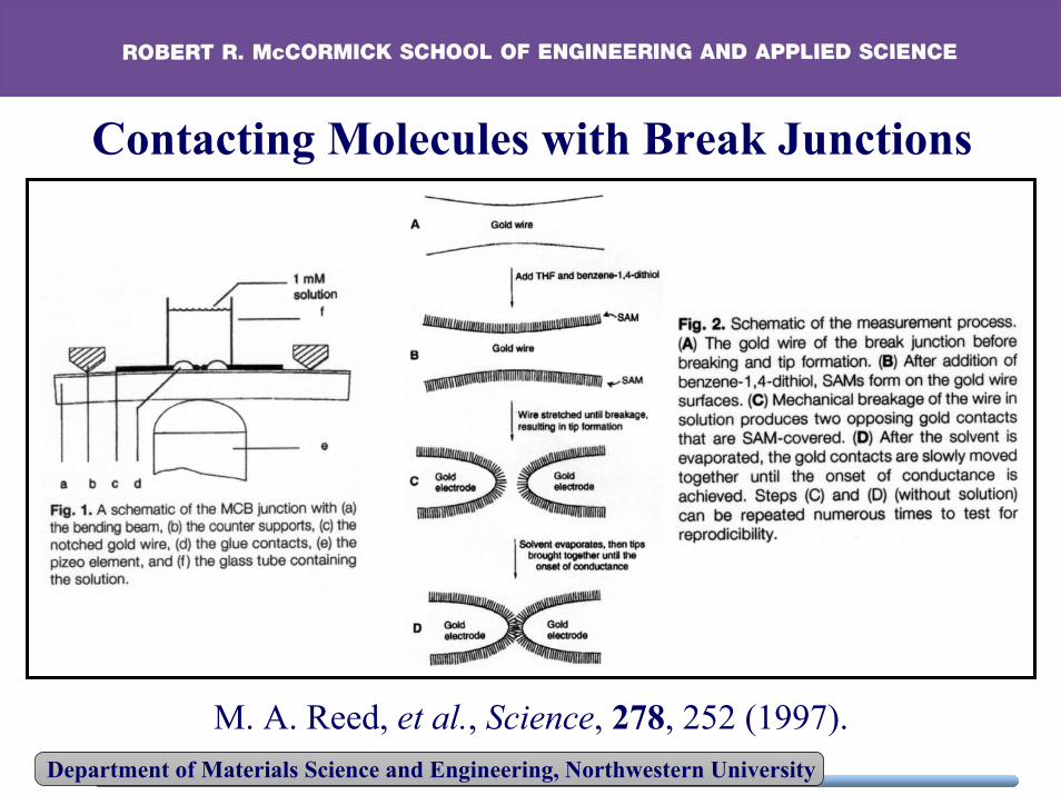
M. A. Reed, et al., Science, 278, 252 (1997).
Contacting Molecules with Break Junctions
Department of Materials Science and Engineering, Northwestern University
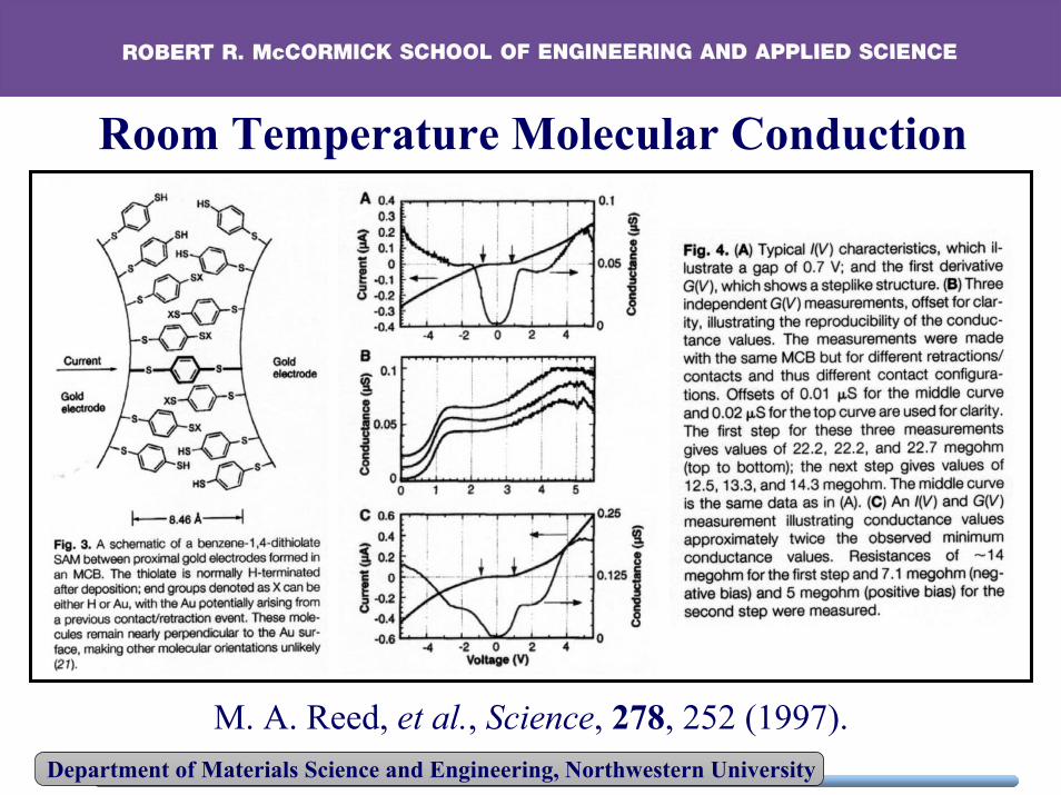
Room Temperature Molecular Conduction
M. A. Reed, et al., Science, 278, 252 (1997).
Department of Materials Science and Engineering, Northwestern University
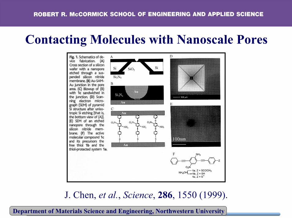
Contacting Molecules with Nanoscale Pores
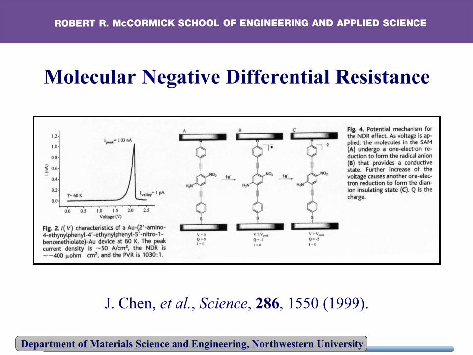
J. Chen, et al., Science, 286, 1550 (1999).
Department of Materials Science and Engineering, Northwestern University
J. Chen, et al., Science, 286, 1550 (1999).
Molecular Negative Differential Resistance
Department of Materials Science and Engineering, Northwestern University
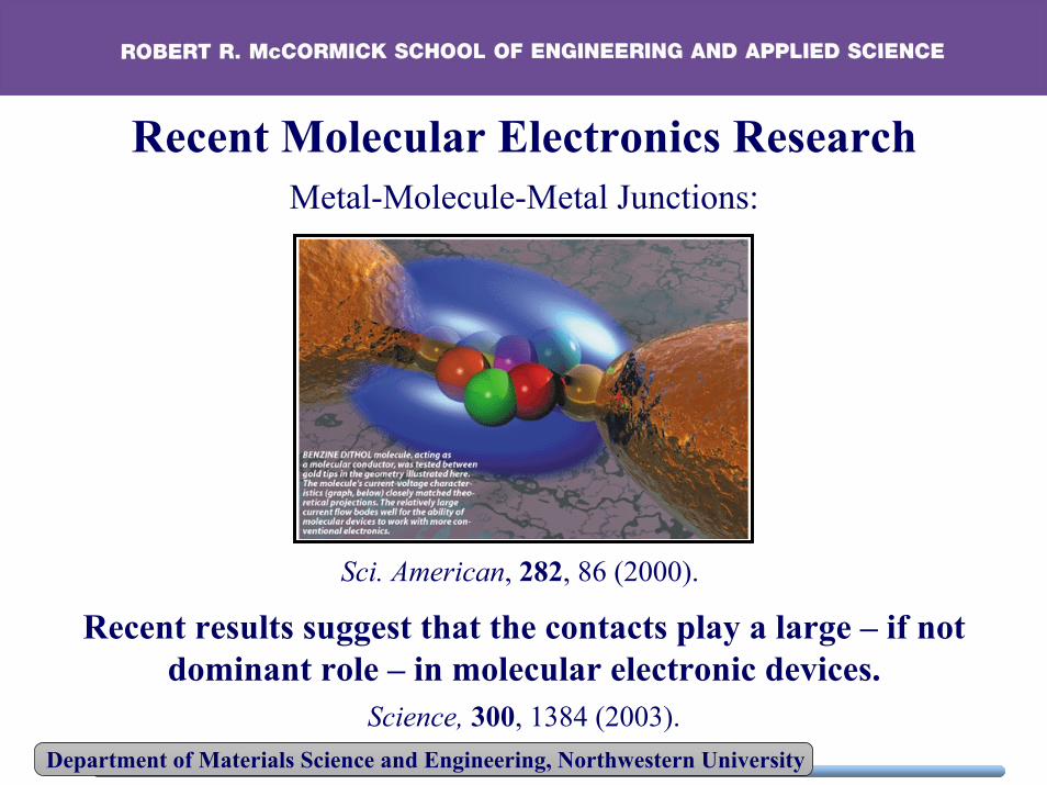
Recent Molecular Electronics Research
Sci. American, 282, 86 (2000).
Metal-Molecule-Metal Junctions:
Recent results suggest that the contacts play a large – if not dominant role – in molecular electronic devices.
Science, 300, 1384 (2003).
Department of Materials Science and Engineering, Northwestern University
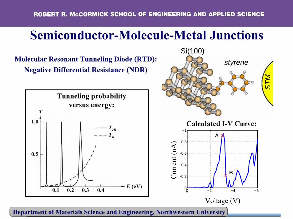
Semiconductor-Molecule-Metal Junctions
−6−4−20
−1
−0.8
−0.6
−0.4
−0.2
0
Applied Voltage
Cur
rent
(μA
)
A
BC
urre
nt (n
A)
Voltage (V)
Calculated I-V Curve:
Molecular Resonant Tunneling Diode (RTD):Negative Differential Resistance (NDR)
Tunneling probabilityversus energy:
styrene
STM
Si(100)
Department of Materials Science and Engineering, Northwestern University
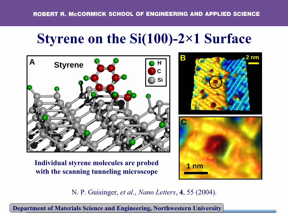
Styrene on the Si(100)-2×1 Surface
1 nm
C
A Styrene HCSi
2 nmB
Individual styrene molecules are probedwith the scanning tunneling microscope
N. P. Guisinger, et al., Nano Letters, 4, 55 (2004).
Department of Materials Science and Engineering, Northwestern University
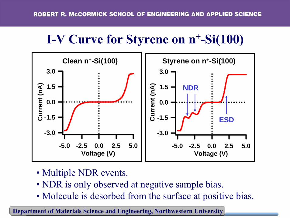
I-V Curve for Styrene on n+-Si(100)
• Multiple NDR events.• NDR is only observed at negative sample bias. • Molecule is desorbed from the surface at positive bias.
-3.0
-1.5
0.0
1.5
3.0
Cur
rent
(nA
)-5.0 -2.5 0.0 2.5 5.0
Voltage (V)
Styrene on n+-Si(100)
NDR
ESD
-3.0
-1.5
0.0
1.5
3.0
Cur
rent
(nA
)
-5.0 -2.5 0.0 2.5 5.0Voltage (V)
Clean n+-Si(100)

Department of Materials Science and Engineering, Northwestern University
TEMPO on the Si(100)-2×1 SurfaceB 3 nm
1 nm
C
A TEMPO NO
HCSi
TEMPO resists electron stimulated desorptionsince it is a saturated hydrocarbon
TEMPO:(2,2,6,6-tetramethyl-1-piperidinyloxy)
N. P. Guisinger, et al., Nano Letters, 4, 55 (2004).
Department of Materials Science and Engineering, Northwestern University
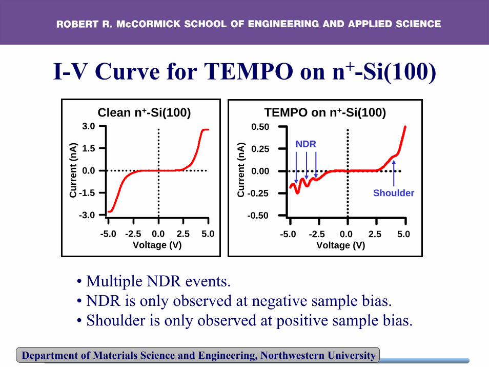
I-V Curve for TEMPO on n+-Si(100)
-0.50
-0.25
0.00
0.25
0.50
Cur
rent
(nA
)-5.0 -2.5 0.0 2.5 5.0
Voltage (V)
TEMPO on n+-Si(100)
NDR
Shoulder
-3.0
-1.5
0.0
1.5
3.0
Cur
rent
(nA
)
-5.0 -2.5 0.0 2.5 5.0Voltage (V)
Clean n+-Si(100)
• Multiple NDR events.• NDR is only observed at negative sample bias. • Shoulder is only observed at positive sample bias.
Department of Materials Science and Engineering, Northwestern University
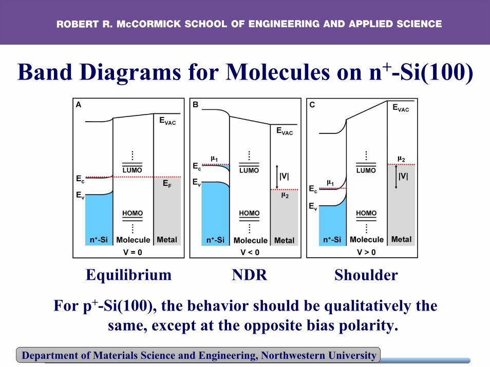
Band Diagrams for Molecules on n+-Si(100)
Equilibrium NDR Shoulder
For p+-Si(100), the behavior should be qualitatively the same, except at the opposite bias polarity.
Department of Materials Science and Engineering, Northwestern University
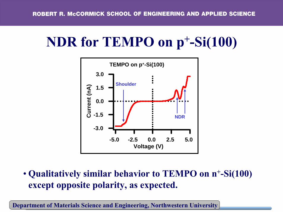
TEMPO on p+-Si(100)
-3.0
-1.5
0.0
1.5
3.0
Cur
rent
(nA
)
-5.0 -2.5 0.0 2.5 5.0Voltage (V)
NDR
Shoulder
NDR for TEMPO on p+-Si(100)
• Qualitatively similar behavior to TEMPO on n+-Si(100) except opposite polarity, as expected.
Department of Materials Science and Engineering, Northwestern University
Molecular Electronics
To become commercially viable, many obstacles must be overcome:
(1) Macroscopic contacts, interconnections
(2) Integration with conventional devices
(3) Reliability
(4) Reproducibility
Defect tolerant architectures and nanotube electronics helpcircumvent some of these problems

Department of Materials Science and Engineering, Northwestern University
J. R. Heath, et al., Science, 280, 1716 (1998).
Department of Materials Science and Engineering, Northwestern University
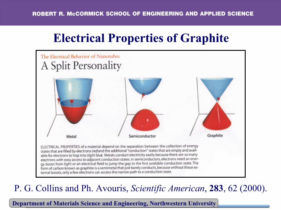
P. G. Collins and Ph. Avouris, Scientific American, 283, 62 (2000).
Electrical Properties of Graphite
Department of Materials Science and Engineering, Northwestern University
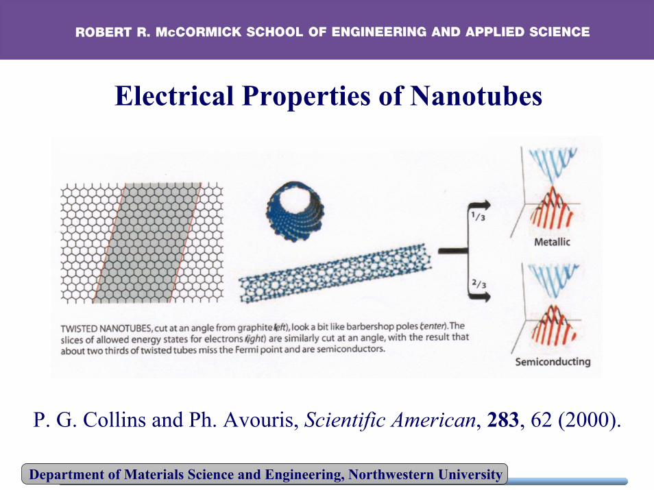
P. G. Collins and Ph. Avouris, Scientific American, 283, 62 (2000).
Electrical Properties of Nanotubes
Department of Materials Science and Engineering, Northwestern University
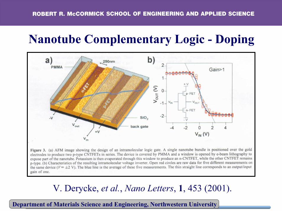
Nanotube Complementary Logic - Doping
V. Derycke, et al., Nano Letters, 1, 453 (2001).
Department of Materials Science and Engineering, Northwestern University
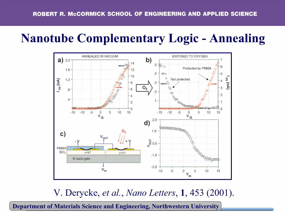
V. Derycke, et al., Nano Letters, 1, 453 (2001).
Nanotube Complementary Logic - Annealing
Department of Materials Science and Engineering, Northwestern University
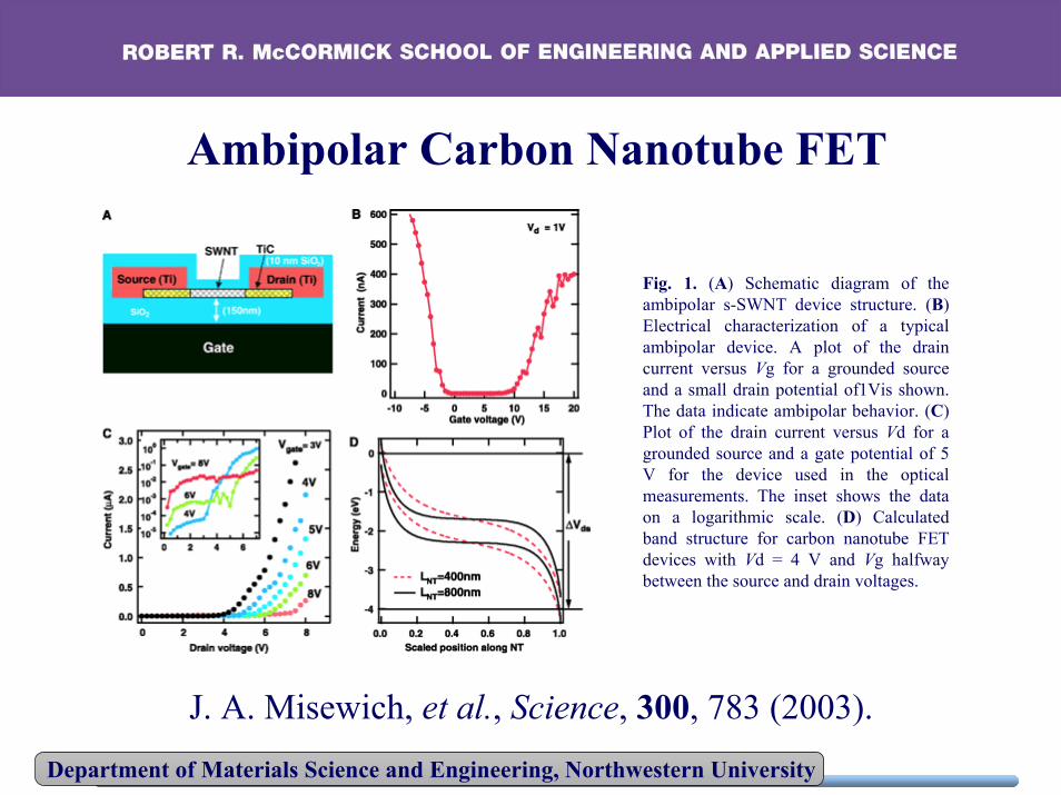
Fig. 1. (A) Schematic diagram of the ambipolar s-SWNT device structure. (B) Electrical characterization of a typical ambipolar device. A plot of the drain current versus Vg for a grounded source and a small drain potential of1Vis shown. The data indicate ambipolar behavior. (C) Plot of the drain current versus Vd for a grounded source and a gate potential of 5 V for the device used in the optical measurements. The inset shows the data on a logarithmic scale. (D) Calculated band structure for carbon nanotube FET devices with Vd = 4 V and Vg halfway between the source and drain voltages.
J. A. Misewich, et al., Science, 300, 783 (2003).
Ambipolar Carbon Nanotube FET
Department of Materials Science and Engineering, Northwestern University
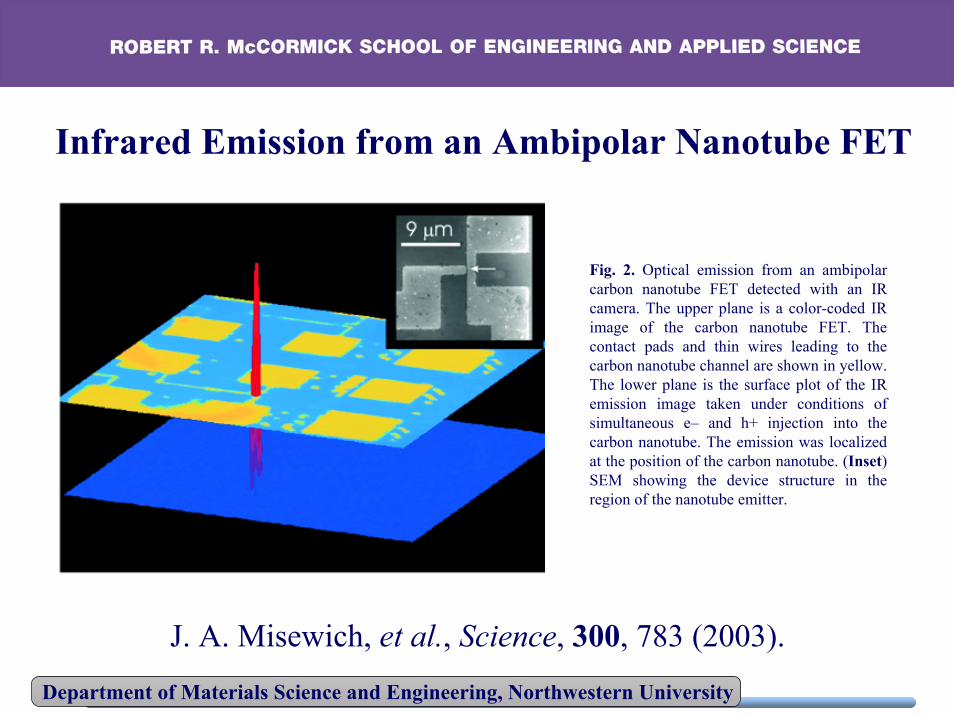
Fig. 2. Optical emission from an ambipolar carbon nanotube FET detected with an IR camera. The upper plane is a color-coded IR image of the carbon nanotube FET. The contact pads and thin wires leading to the carbon nanotube channel are shown in yellow. The lower plane is the surface plot of the IR emission image taken under conditions of simultaneous e– and h+ injection into the carbon nanotube. The emission was localized at the position of the carbon nanotube. (Inset) SEM showing the device structure in the region of the nanotube emitter.
Infrared Emission from an Ambipolar Nanotube FET
J. A. Misewich, et al., Science, 300, 783 (2003).
Department of Materials Science and Engineering, Northwestern University
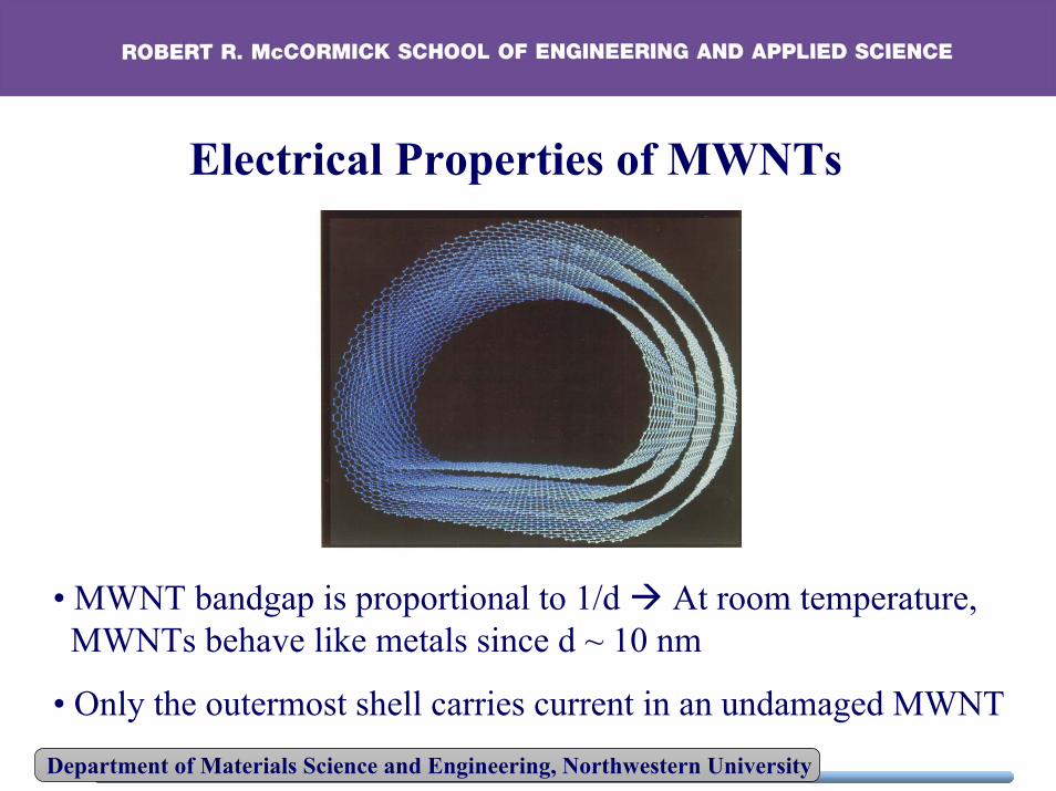
Electrical Properties of MWNTs
• MWNT bandgap is proportional to 1/d At room temperature,MWNTs behave like metals since d ~ 10 nm
• Only the outermost shell carries current in an undamaged MWNT
Department of Materials Science and Engineering, Northwestern University
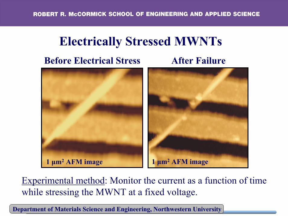
Electrically Stressed MWNTs
Experimental method: Monitor the current as a function of timewhile stressing the MWNT at a fixed voltage.
Before Electrical Stress
1 μm2 AFM image
After Failure
1 μm2 AFM image
Department of Materials Science and Engineering, Northwestern University
8
6
4
2
0
Cur
rent
dens
ity(x
1013
A/m
2 )
1614121086420Electric field (x106 V/m)
Maximum current density: 6.8 x 10¹³ A/m2
Maximum electric field: 1.6 x 10⁷ V/m
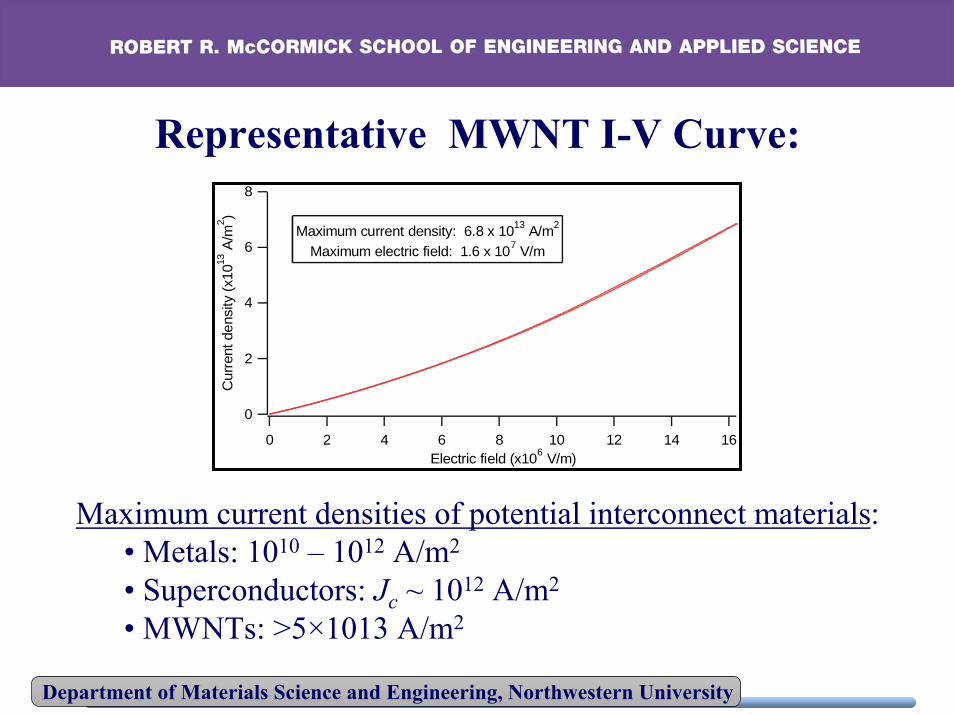
Representative MWNT I-V Curve:
Maximum current densities of potential interconnect materials:• Metals: 1010 – 1012 A/m2
• Superconductors: Jc ~ 1012 A/m2
• MWNTs: >5×10¹³ A/m2

Department of Materials Science and Engineering, Northwestern University
Multiwalled Carbon Nanotube Failure
P. G. Collins, M. C. Hersam, M. Arnold, R. Martel, and Ph. Avouris, Phys. Rev. Lett., 86, 3128 (2001).
Department of Materials Science and Engineering, Northwestern University
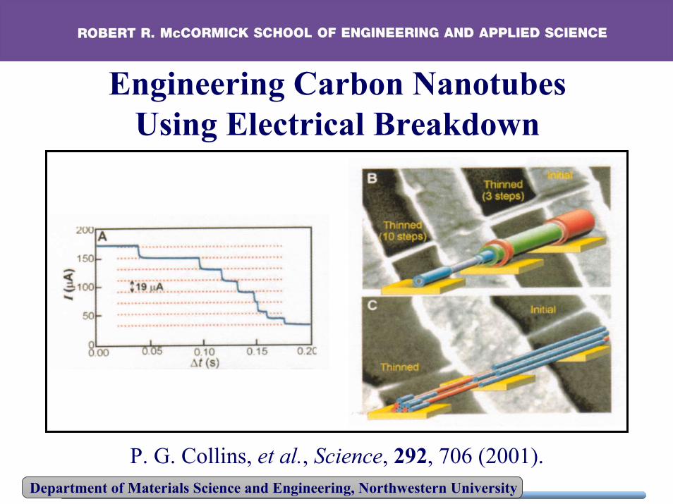
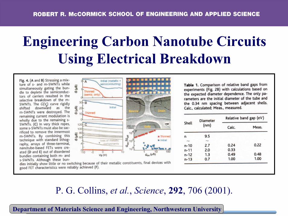
P. G. Collins, et al., Science, 292, 706 (2001).
Engineering Carbon NanotubesUsing Electrical Breakdown
Department of Materials Science and Engineering, Northwestern University
P. G. Collins, et al., Science, 292, 706 (2001).
Engineering Carbon Nanotube CircuitsUsing Electrical Breakdown