Embed Size (px)
Citation preview
October 24, 2016 1
www.bruker.com
NanoForce
-short note -
Ilja Hermann

October 24, 2016 2
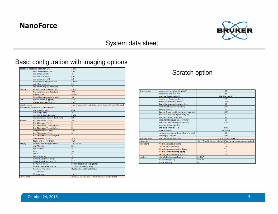
NanoForce
System overview
• Electromagnetic actuator (indentation loads between 0.2 uN and 45 mN) • Three-plate capacitor (indentation depth up to 40 um)• Load control • Depth- and strain-rate control by S/W feedback control• Berkovich tip is included; misc. different indenter geometries optional; easy switch • In-line microscope with coaxial turret optics and AFM are standard• Automatic multi-specimen handling (magnetic, vacuum, mech. clamp mounting)
Coaxial optical lenses and AFM
Thermal/Acoustic/Seismic hood
Internal (3-plate) capacitance sensor housing
Microscope for inspection pre- and pre- and post-test
Actuator housing
Quantitative property assessment: HIT, EIT, E’ , E”, Y, KIC, σRep(εRep), FCrit., topography
Optional vacuum chuck
Specimen tray
October 24, 2016 3
NanoForce
System data sheet
Basic configuration with imaging options
Scratch option

October 24, 2016 4
Typcial Nanoindentation test
AFM & Optical View (post IMG of surface with 9 indents at different surface locations)
Force-Displacement curves(Dynamic indentations at 9 different surface positions)
NanoForce
1. Test positioning
2. Applying the test method (running indent-loading profile and analysis)
3. Post inspection of tested surface area
1.7mm
1.5 um
Indentations
Cube corner into Si (100)
Berkovich into HPFS
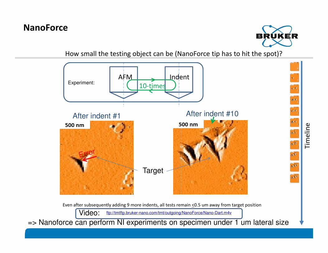
How small the testing object can be (NanoForce tip has to hit the spot)?
Even after subsequently adding 9 more indents, all tests remain <0.5 um away from target position
Tim
eli
ne
NanoForce
IndentAFM
10-timesExperiment:
After indent #1 After indent #10
Target
=> Nanoforce can perform NI experiments on specimen under 1 um lateral size
ftp://tmtftp.bruker-nano.com/tmt/outgoing/NanoForce/Nano-Dart.m4vVideo:
NanoForce
Instrument calibration
October 24, 20167
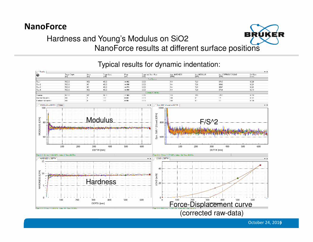
Hardness and Young’s Modulus on SiO2NanoForce results at different surface positions
Typical results for dynamic indentation:
NanoForce
Force-Displacement curve
(corrected raw-data)
F/S^2
Hardness
Modulus
October 24, 2016 8
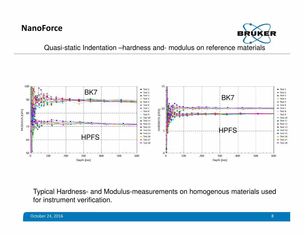
Quasi-static Indentation –hardness and- modulus on reference materials
HPFS
BK7
NanoForce
Typical Hardness- and Modulus-measurements on homogenous materials used
for instrument verification.
HPFS
BK7

NanoForce
Thin film applications
October 24, 2016 10
NanoForce
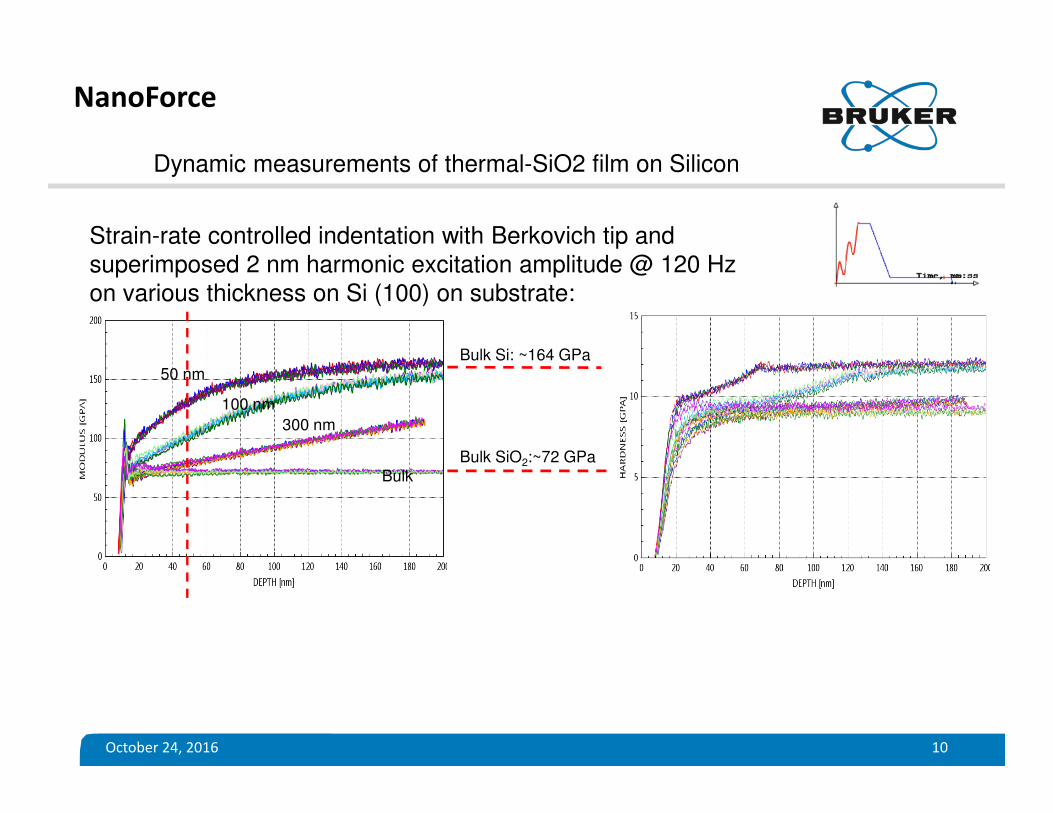
Dynamic measurements of thermal-SiO2 film on Silicon
Strain-rate controlled indentation with Berkovich tip and
superimposed 2 nm harmonic excitation amplitude @ 120 Hz
on various thickness on Si (100) on substrate:
50 nm
100 nm
300 nm
Bulk
Bulk SiO2:~72 GPa
Bulk Si: ~164 GPa
October 24, 2016 11
NanoForce
Brittle material characterization

October 24, 2016 12
Fracture toughness
Nano-indentation results
Method inputs:
E…Young’s modulus
H…hardness
P…test load
a, c, l….distances from imageBerkovich [2]:
Cube Corner [1]:
Step 2: Produce a series of indentations at different loads and surface locations
Step 3: Image indents to find critical load for fully developed set of lead corner radial cracks
Step 4: Calculate Fracture toughness :
Step 1: Measure Hardness and Young’s modulus of the specimen
[1] D. S. Harding, W. C. Oliver and G. M. Pharr: Mat. Res. Soc. Symp. Proc., 356, 1995, 663.
[2] R. Dukino and M.V. Swain, J. Am. Ceram. Soc. 75 12, 1992, 3299

October 24, 2016 13
NanoForce
Characterization of metallic single crystals
October 24, 2016 14
NanoForce
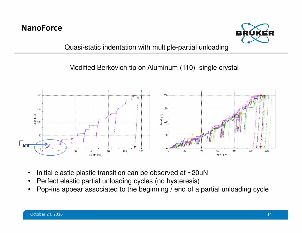
• Initial elastic-plastic transition can be observed at ~20uN
• Perfect elastic partial unloading cycles (no hysteresis)
• Pop-ins appear associated to the beginning / end of a partial unloading cycle
Quasi-static indentation with multiple-partial unloading
Modified Berkovich tip on Aluminum (110) single crystal
Fkrit

October 24, 2016 15
NanoForce
Dynamic indentation on single crystals:
Cu (110)Cu (111)
• The (111) orientation appears stiffer than the (110) orientation
• The (111) orientation exhibits pop-in events at approx. 10 uN load
Fkrit
Cube Corner tip on Copper (110) and (111) orientations

October 24, 2016 16
NanoForce
Indentation Creep
October 24, 2016 17
NanoForce
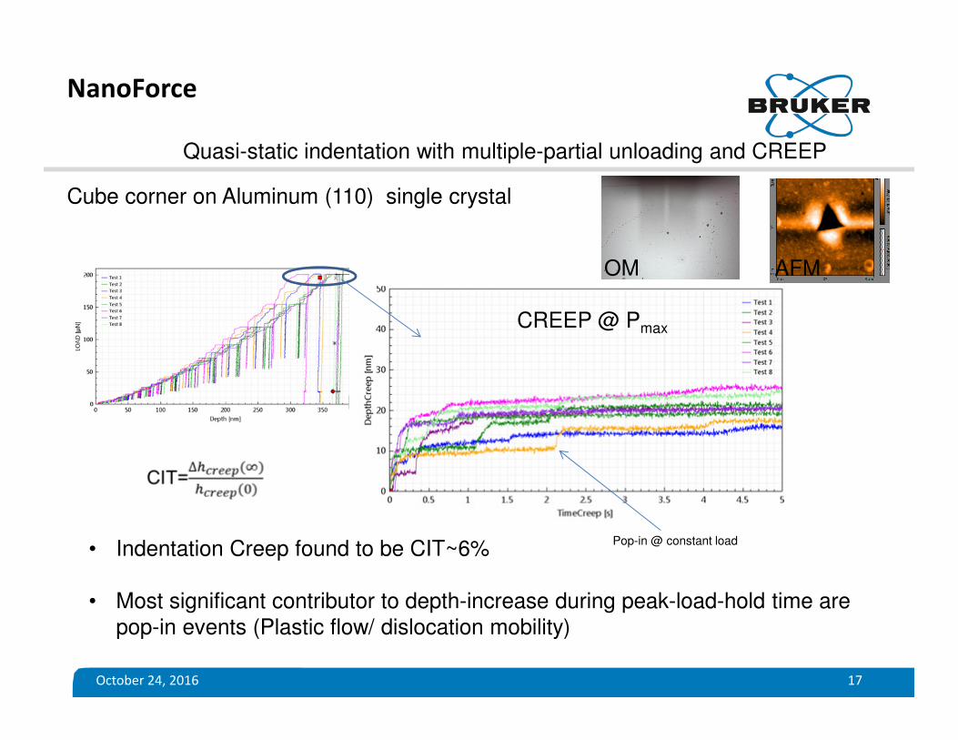
• Indentation Creep found to be CIT~6%
• Most significant contributor to depth-increase during peak-load-hold time are
pop-in events (Plastic flow/ dislocation mobility)
Quasi-static indentation with multiple-partial unloading and CREEP
Cube corner on Aluminum (110) single crystal
OM AFM
CREEP @ Pmax
Pop-in @ constant load

October 24, 2016 18
NanoForce
(Soft) Polymers
October 24, 2016 19
NanoForce
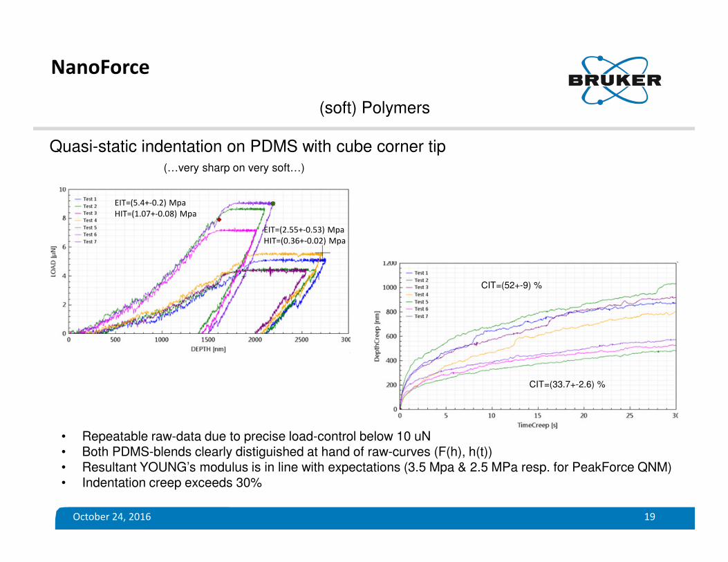
(soft) Polymers
Quasi-static indentation on PDMS with cube corner tip(…very sharp on very soft…)
EIT=(5.4+-0.2) Mpa
HIT=(1.07+-0.08) Mpa
EIT=(2.55+-0.53) Mpa
HIT=(0.36+-0.02) Mpa
CIT=(52+-9) %
CIT=(33.7+-2.6) %
• Repeatable raw-data due to precise load-control below 10 uN• Both PDMS-blends clearly distiguished at hand of raw-curves (F(h), h(t))• Resultant YOUNG’s modulus is in line with expectations (3.5 Mpa & 2.5 MPa resp. for PeakForce QNM)• Indentation creep exceeds 30%

October 24, 2016 20
NanoForce
Adhesion

October 24, 2016 21
NanoForce
Adhesion
Quasi-static indentation on PDMS with 50 um conical tip
Obtain quantitative data : • DMT modulus , starting @ ~1 Mpa• Adhesion • Energy dissipation• Surface deformation
Adhesionrindenter PRdEP +=3
3
4
Tip-stiction forces was measured @ approach (and pull-off) down to 2.5 um radius
Contact model with stiction (DMT)
Nano-Indenter gives
insights into new more
complex contact physics:
R=50um
R=5 um
R=2.5 um

October 24, 2016 22
NanoForce
Scratch

NanoForce
Micro-Scratch
• 5x scratch into AL(110) Length 200 um length, lateral strain rate 0.1 Hz , Conical R=5 um, • 50x optical magnification, stitched
progressive load 0.5-10 mN
constant load 10 mN
Repeatability:

NanoForce
Constant load Nano-Scratch – 300 nm SiO2 on Si with Conical 2.5 um
• Pairs of constant load scratch series (1, 3, 5, 7, 10) mN, Length 20 um, 10mN; Strain rate 0.1 Hz
_P130
topography (NanoLens) 1-D profile through scratch series

NanoForce
Nano-Scratch
1x progressive load scratch; 0.5-10 mN; Length 20 um length, Strain rate 0.1 Hz; Conical R=5 um
25 nm ITO on PET
30 nm SiO2 on PET

NanoForce
Nano-Scratch
2x progressive load scratch; 0.5-50 mN; Length 20 um length, Strain rate 0.1 Hz; Conical R=5 um
24 nm brittle film on Si
Fcrit~44mN
Instrumented scratch data:
Longitudinal Profiling @ load

NanoForce
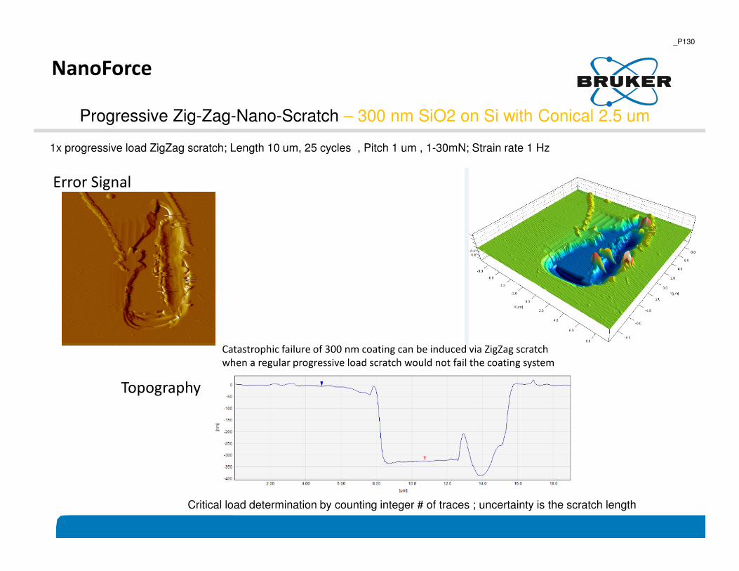
Progressive Zig-Zag-Micro-Scratch – 300 nm SiO2 on Si with Conical 2.5 um
Fcrit~25 mN
Stage Motion Trajectory
1x progressive load ZigZag scratch; Length 50 um, 25 cycles , Pitch 1 um , 1-50mN; lateral strain rate 1 Hz
_P130

NanoForce
Progressive Zig-Zag-Micro-Scratch – 300 nm SiO2 on Si with Conical 2.5 um
Failure event identification by tip-profiling
• 1x progressive load ZigZag scratch; Length 50 um, 25 cycles , Pitch 1 um , 1-30mN; lateral Strain rate 1 Hz
• Transversal post-profiling with indenter tip @ average profiling loads ca. 2 uN
_P130
Cleaned from debris
ZigZag-Trajectory
Straight Trajectory
Topography
Profiling load stability
Critical load determination e.g. by counting integer # of traces ; uncertainty is
the scratch length
Note: Regular progressive scratch shows no failure while ZigZag
scratch promotes this @ same range of load variation
NanoForce
Progressive Zig-Zag-Nano-Scratch – 300 nm SiO2 on Si with Conical 2.5 um
Catastrophic failure of 300 nm coating can be induced via ZigZag scratch
when a regular progressive load scratch would not fail the coating system
1x progressive load ZigZag scratch; Length 10 um, 25 cycles , Pitch 1 um , 1-30mN; Strain rate 1 Hz
_P130
Topography
Critical load determination by counting integer # of traces ; uncertainty is the scratch length
Error Signal

October 24, 2016 30
NanoForce
Other misc. applications
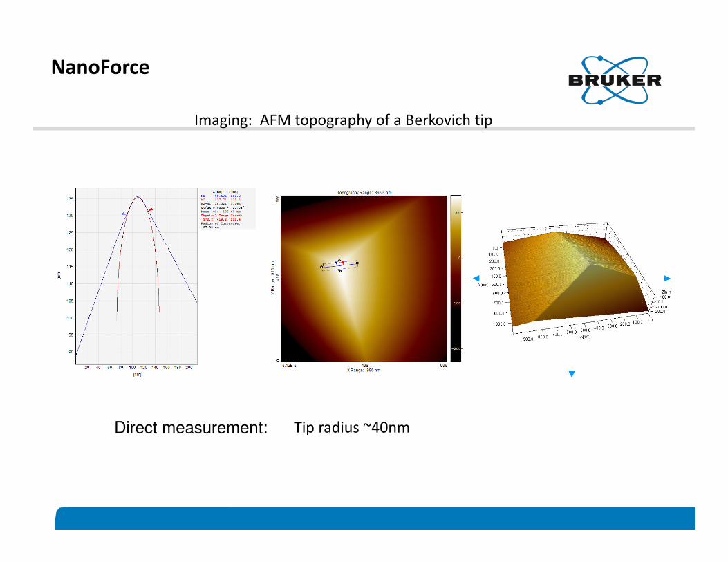
Imaging: AFM topography of a Berkovich tip
Tip radius ~40nm
NanoForce
Direct measurement:

October 24, 2016 32
NanoForce
Precision of head mount and Indenter tip mounting
Cube Corner tip => Berkovich tip
Berkovich Tip => Conical tip
• mod. Berkovich
• Cube Corner
• Vickers
• Conical R=Var
• Flat Punch R=Var
• …
NanoForce tip shape options:
Requires remove/reinstall tip
Experiment: Measure remaining pos. accuracy after tip change
Quiz:
What if re-cal is skipped?:
Pos error ~7 um
Pos error ~5 um
Answer:
No big problem: pos accuracy remain better 10 um !(…and is this is not enough – best accuracy is just s fe clicks away (no new indent required)
and re-calibrate inline offset

October 24, 2016 33
NanoForce
Hertzian contact
i
Experiment
r
HertzModelS
Fh
RE
Fh −=
=
32
,
4
3
With:• Tip radius R from AFM (calculations with radius as function of depth (R(h))• Best Fit for 3 reference materials (Fused Silica, Sapphire 0001 and Si 100)
Extraction of Load-Frame stiffness from Hertzian contact modeling
Overall system stiffness: ~2.5 N/um
(good agreement with 2.2 N/um from elastic-
plastic indentation (F/S^2))
October 24, 2016 34
NanoForce
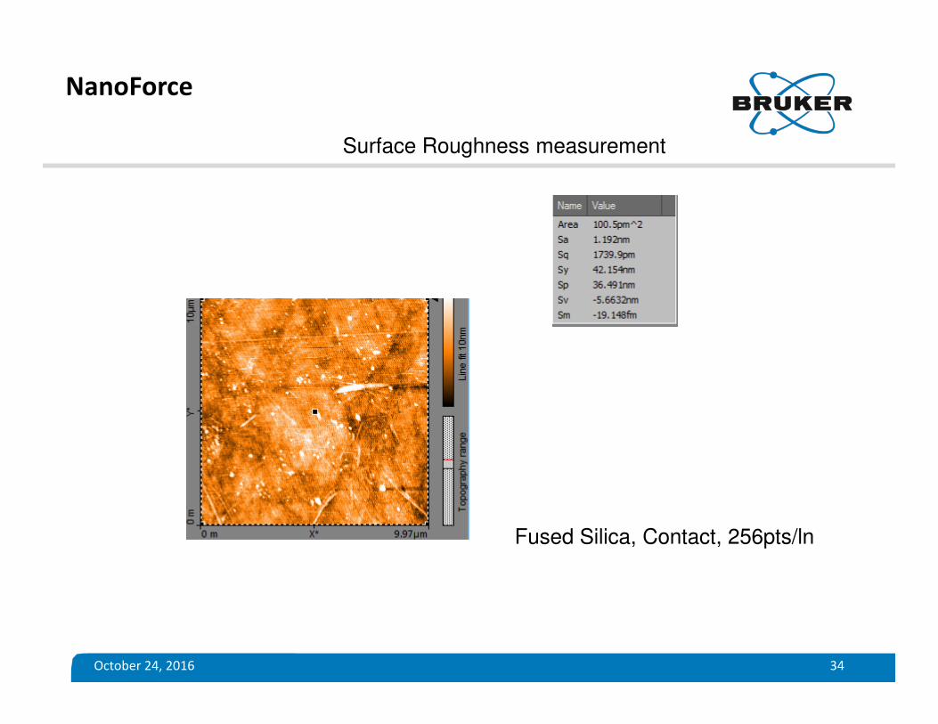
Surface Roughness measurement
Fused Silica, Contact, 256pts/ln

October 24, 2016 35
NanoForce
Optical Microscope
• FOV All pixels
• Resolution ~500nm opt; ~1.7 nm afm scanner
• >3000x total magnification + digital zoom
• Bright-field illumination;
• Optional: Extra objectives & Dark-field
5x2.5x
8x
10x
20x
AFM
optional
Standard
DF
BF
Silicon or smooth, reflective
surfaces in Bright-field…
Skin or rough, absorbing surfaces:
Dark-field…
Vs. dark-field…
2.5x
2.5x50x
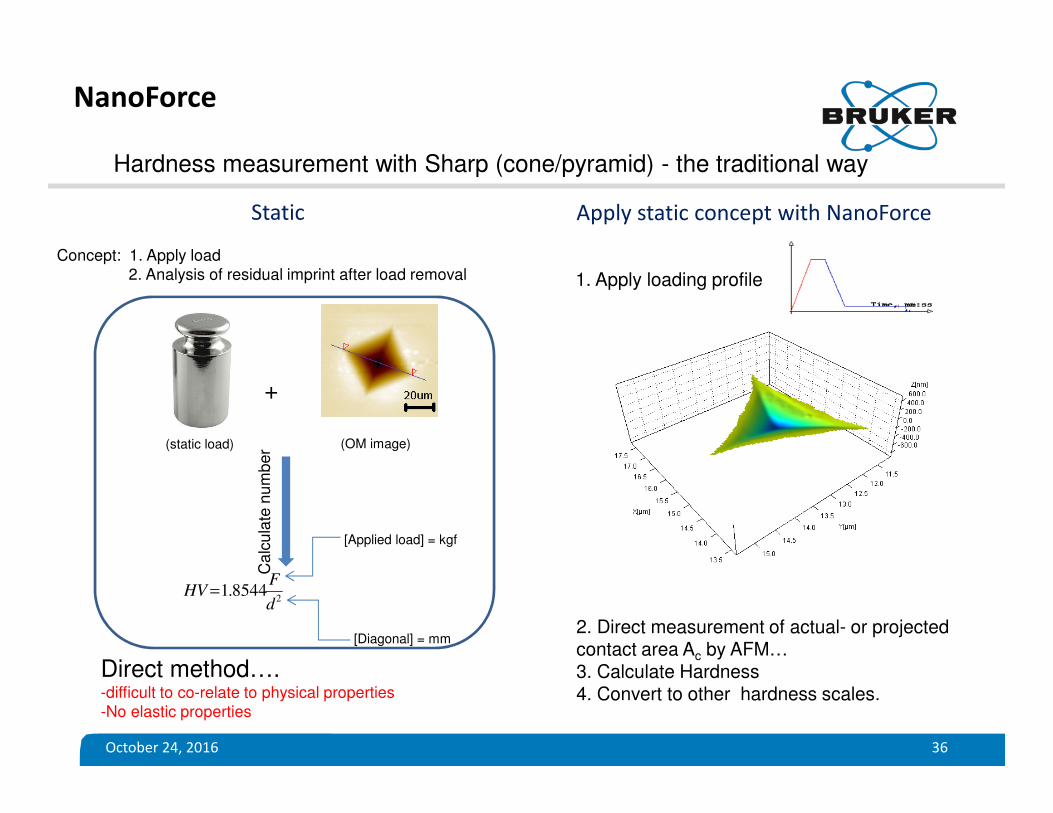
October 24, 2016 36
[Diagonal] = mm
28544.1
d
FHV =
[Applied load] = kgf
Concept: 1. Apply load
2. Analysis of residual imprint after load removal
Direct method…. -difficult to co-relate to physical properties
-No elastic properties
+
(static load) (OM image)
Ca
lcu
late
nu
mb
er
Static Apply static concept with NanoForce
NanoForce
Hardness measurement with Sharp (cone/pyramid) - the traditional way
2. Direct measurement of actual- or projected contact area Ac by AFM…3. Calculate Hardness4. Convert to other hardness scales.
1. Apply loading profile