Embed Size (px)
Citation preview

Nanoimprint Lithography and Applications
Wei Wu
Department of Electrical Engineering
University of Southern California
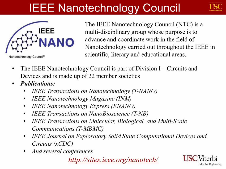
IEEE Nanotechnology Council
The IEEE Nanotechnology Council (NTC) is a multi-disciplinary group whose purpose is to advance and coordinate work in the field of Nanotechnology carried out throughout the IEEE in scientific, literary and educational areas.
• The IEEE Nanotechnology Council is part of Division I – Circuits and Devices and is made up of 22 member societies
• Publications:• IEEE Transactions on Nanotechnology (T-NANO)• IEEE Nanotechnology Magazine (INM)• IEEE Nanotechnology Express (ENANO)• IEEE Transactions on NanoBioscience (T-NB)• IEEE Transactions on Molecular, Biological, and Multi-Scale
Communications (T-MBMC)• IEEE Journal on Exploratory Solid State Computational Devices and
Circuits (xCDC)• And several conferences
http://sites.ieee.org/nanotech/
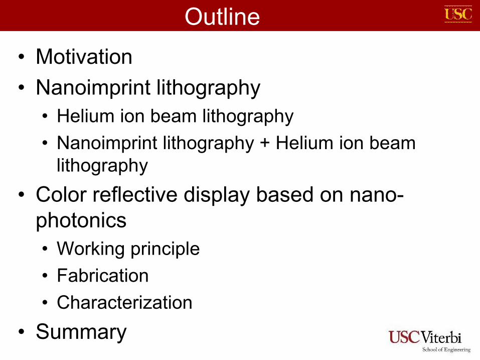
Outline
• Motivation
• Nanoimprint lithography
• Helium ion beam lithography
• Nanoimprint lithography + Helium ion beam lithography
• Color reflective display based on nano-photonics
• Working principle
• Fabrication
• Characterization
• Summary
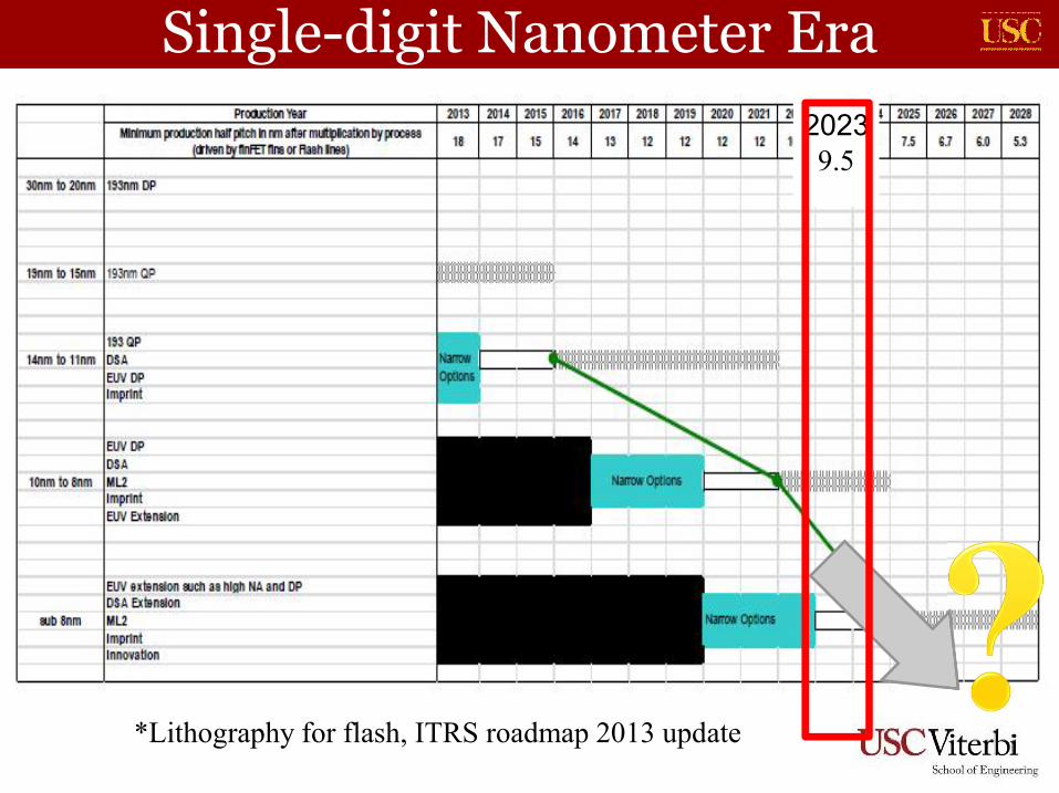
Single-digit Nanometer Era
*Lithography for flash, ITRS roadmap 2013 update
20239.5
Source: Britney Spears guide to Semiconductor Physics
http://britneyspears.ac/lasers.htm
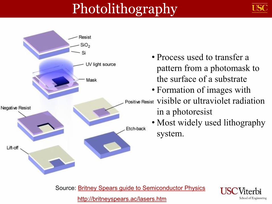
Photolithography
• Process used to transfer a pattern from a photomask to the surface of a substrate
• Formation of images with visible or ultraviolet radiation in a photoresist
• Most widely used lithography system.
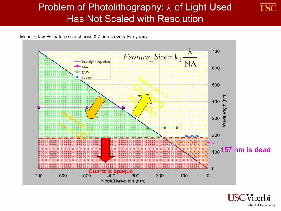
Problem of Photolithography: of Light Used Has Not Scaled with Resolution
Moore’s law feature size shrinks 0.7 times every two years
0
100
200
300
400
500
600
700
0100200300400500600700Node/Half-pitch (nm)
Wave
length
(nm
)
Rayleigh's equation
I-line
DUV
193 nm
NA
λk_ 1SizeFeature
Quartz is opaque
157 nm is dead
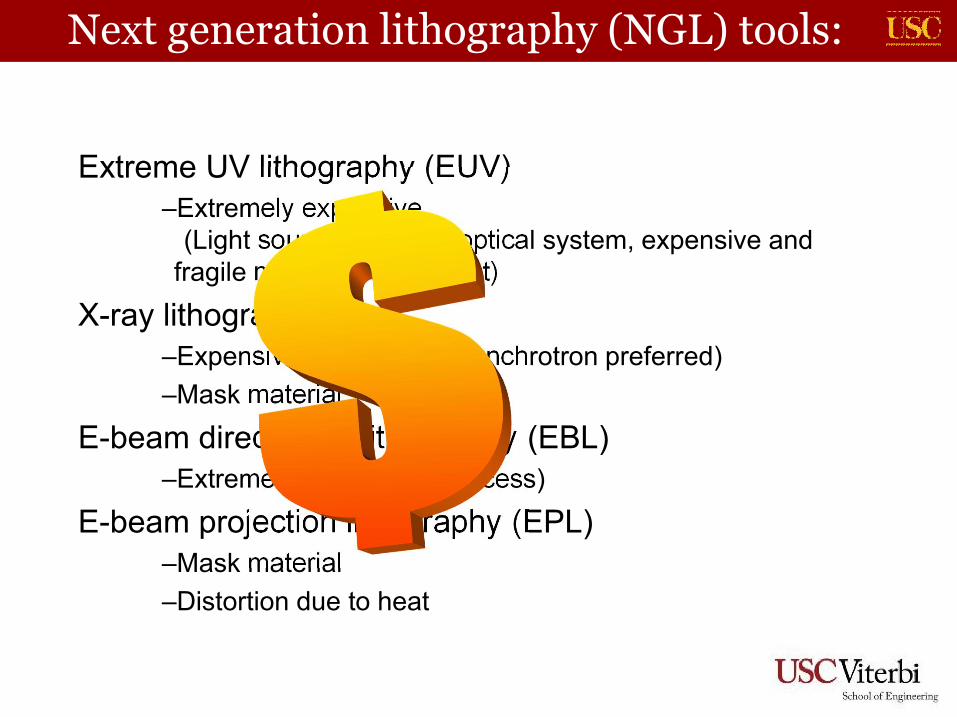
Next generation lithography (NGL) tools:
Extreme UV lithography (EUV)–Extremely expensive
(Light source, complex optical system, expensive and fragile mask, defects count)
X-ray lithography–Expensive light source (synchrotron preferred)
–Mask material
E-beam direct write lithography (EBL)–Extremely slow (serial process)
E-beam projection lithography (EPL)–Mask material
–Distortion due to heat
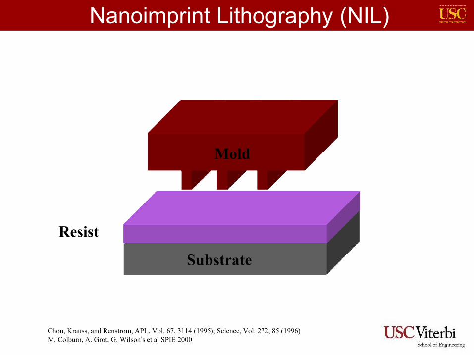
Resist
Mold
Substrate
Nanoimprint Lithography (NIL)
Chou, Krauss, and Renstrom, APL, Vol. 67, 3114 (1995); Science, Vol. 272, 85 (1996)M. Colburn, A. Grot, G. Wilson’s et al SPIE 2000

Substrate
Resist
Mold
Substrate
Nanoimprint Lithography (NIL)
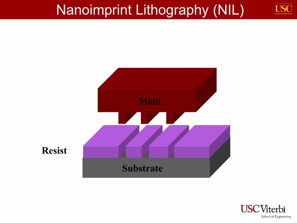
Substrate
Resist
Mold
Substrate
Nanoimprint Lithography (NIL)
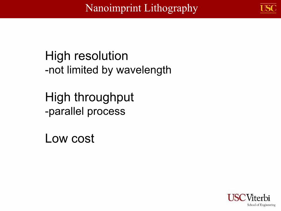
Nanoimprint Lithography
High resolution-not limited by wavelength
High throughput -parallel process
Low cost
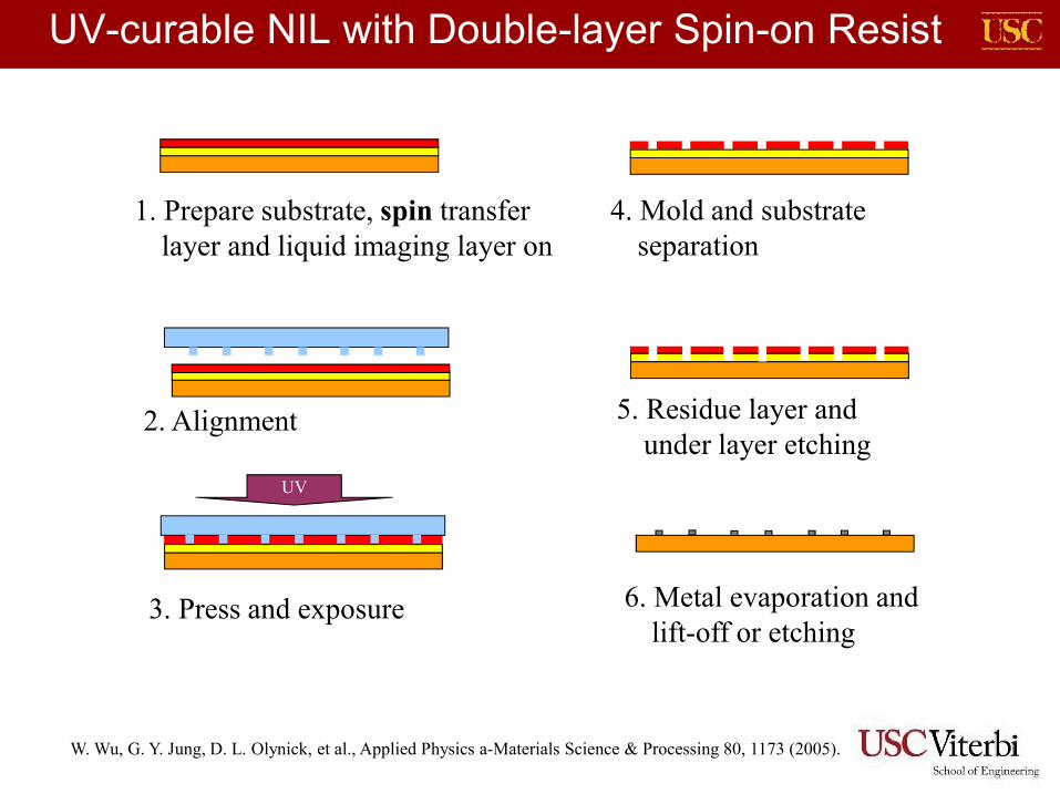
UV-curable NIL with Double-layer Spin-on Resist
UV
W. Wu, G. Y. Jung, D. L. Olynick, et al., Applied Physics a-Materials Science & Processing 80, 1173 (2005).
1. Prepare substrate, spin transfer layer and liquid imaging layer on
2. Alignment
3. Press and exposure
4. Mold and substrate separation
5. Residue layer and under layer etching
6. Metal evaporation and lift-off or etching
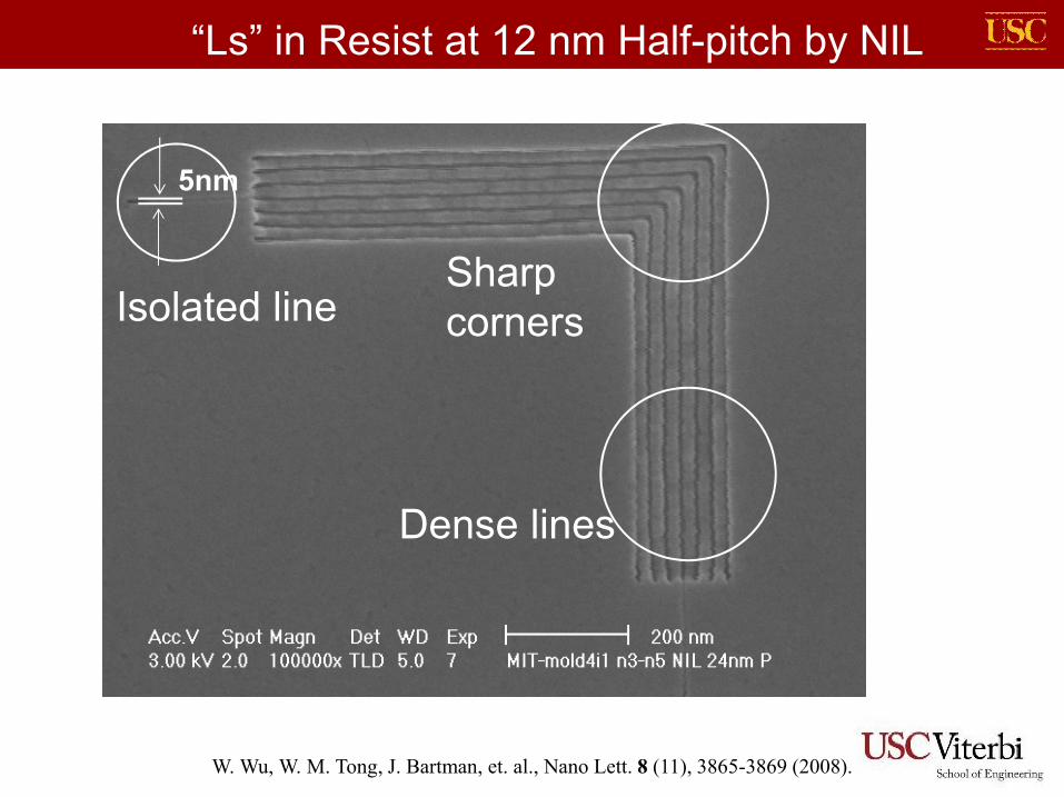
“Ls” in Resist at 12 nm Half-pitch by NIL
Dense lines
Isolated lineSharp corners
W. Wu, W. M. Tong, J. Bartman, et. al., Nano Lett. 8 (11), 3865-3869 (2008).
5nm
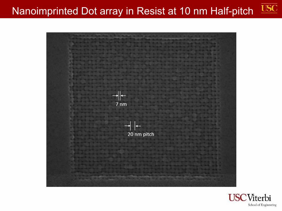
Nanoimprinted Dot array in Resist at 10 nm Half-pitch
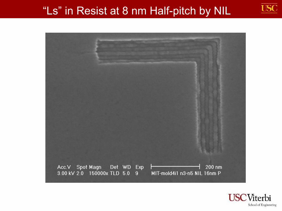
“Ls” in Resist at 8 nm Half-pitch by NIL
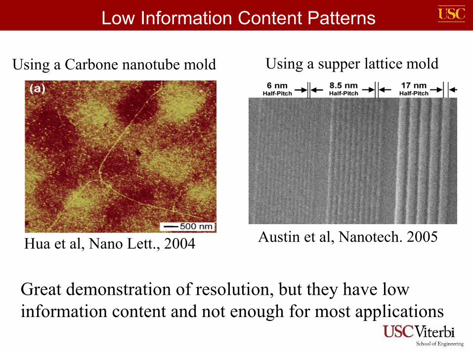
Hua et al, Nano Lett., 2004 Austin et al, Nanotech. 2005
Low Information Content Patterns
Using a Carbone nanotube mold Using a supper lattice mold
Great demonstration of resolution, but they have low information content and not enough for most applications
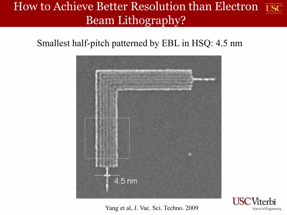
How to Achieve Better Resolution than Electron Beam Lithography?
Smallest half-pitch patterned by EBL in HSQ: 4.5 nm
Yang et al, J. Vac. Sci. Techno. 2009
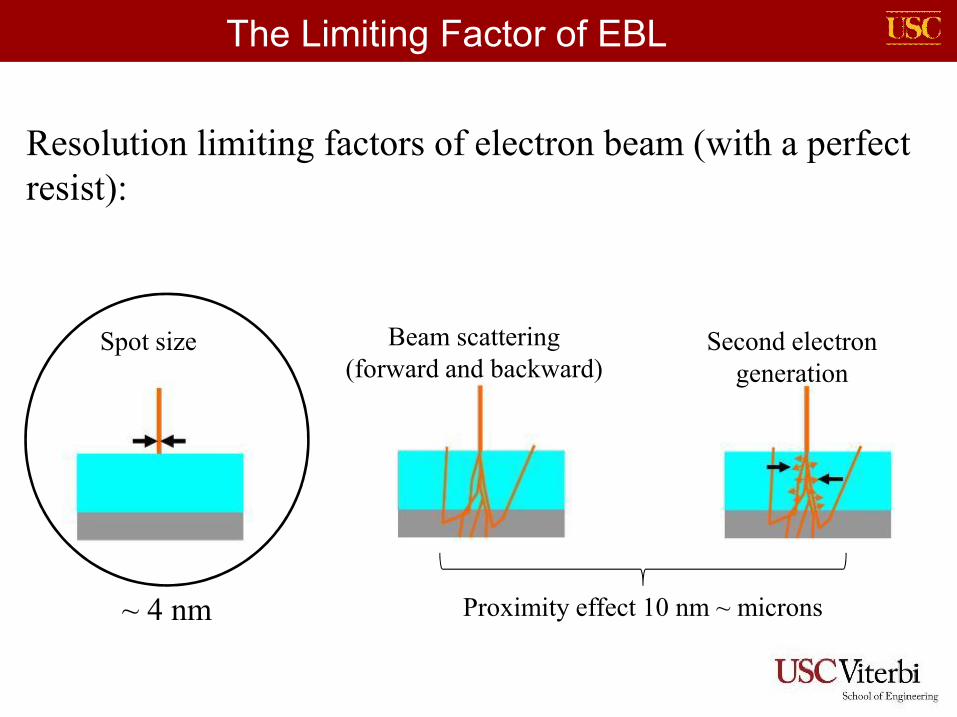
The Limiting Factor of EBL
Resolution limiting factors of electron beam (with a perfect resist):
Beam scattering (forward and backward)
Second electron generation
Proximity effect 10 nm ~ microns
Spot size
~ 4 nm
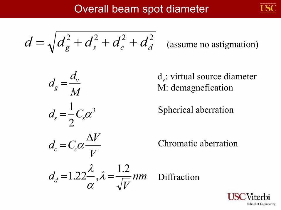
Overall beam spot diameter
2222dcsg ddddd
nmV
d
V
VCd
Cd
M
dd
d
cc
ss
vg
2.1,22.1
2
1 3
dv: virtual source diameterM: demagnefication
Spherical aberration
Chromatic aberration
Diffraction
(assume no astigmation)
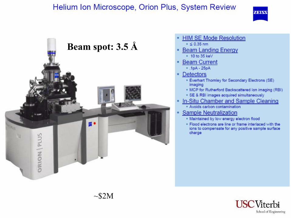
Beam spot: 3.5 Å
~$2M
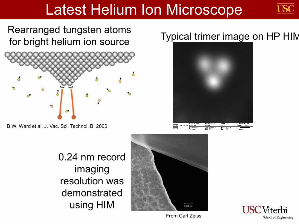
Latest Helium Ion Microscope
Typical trimer image on HP HIM
B.W. Ward et al, J. Vac. Sci. Technol. B, 2006
Rearranged tungsten atoms for bright helium ion source
0.24 nm record imaging
resolution was demonstrated
using HIM From Carl Zeiss

Overall beam spot diameter
2222dcsg ddddd
nmV
d
V
VCd
Cd
M
dd
d
cc
ss
vg
2.1,22.1
2
1 3
dv: virtual source diameterM: demagnefication
Spherical aberration
Chromatic aberration
Diffraction
(assume no astigmation)
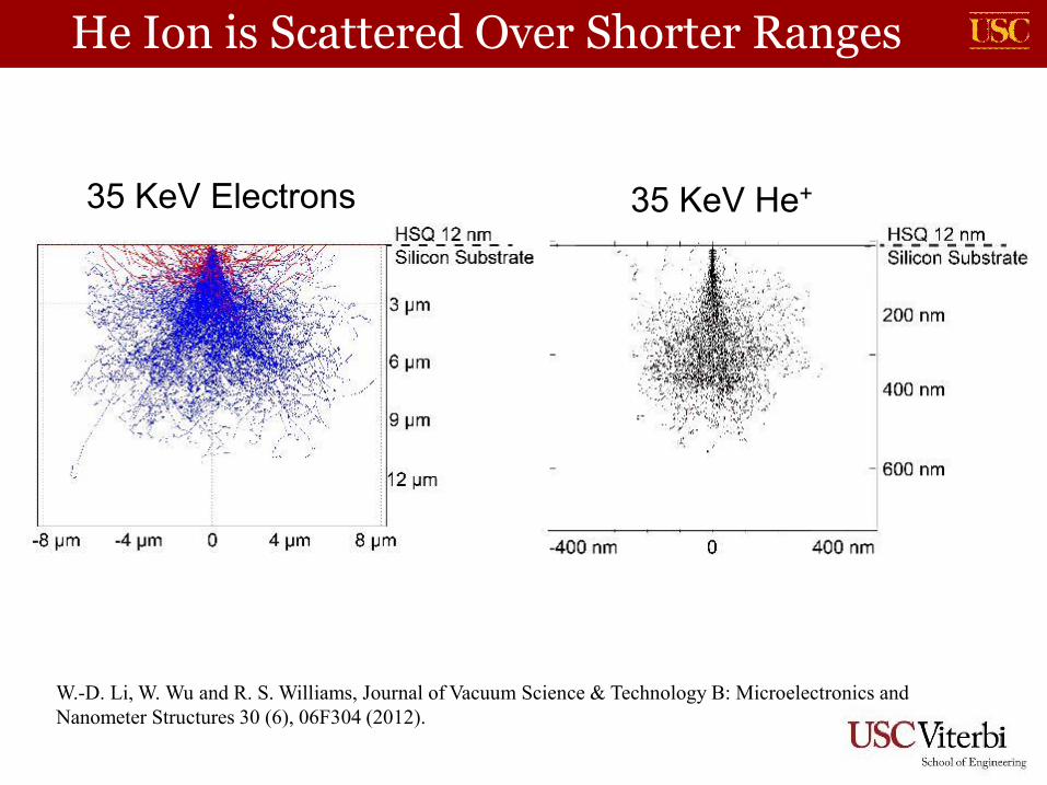
35 KeV Electrons 35 KeV He+
He Ion is Scattered Over Shorter Ranges
W.-D. Li, W. Wu and R. S. Williams, Journal of Vacuum Science & Technology B: Microelectronics and Nanometer Structures 30 (6), 06F304 (2012).
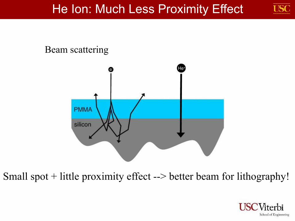
He Ion: Much Less Proximity Effect
Beam scattering
Small spot + little proximity effect --> better beam for lithography!
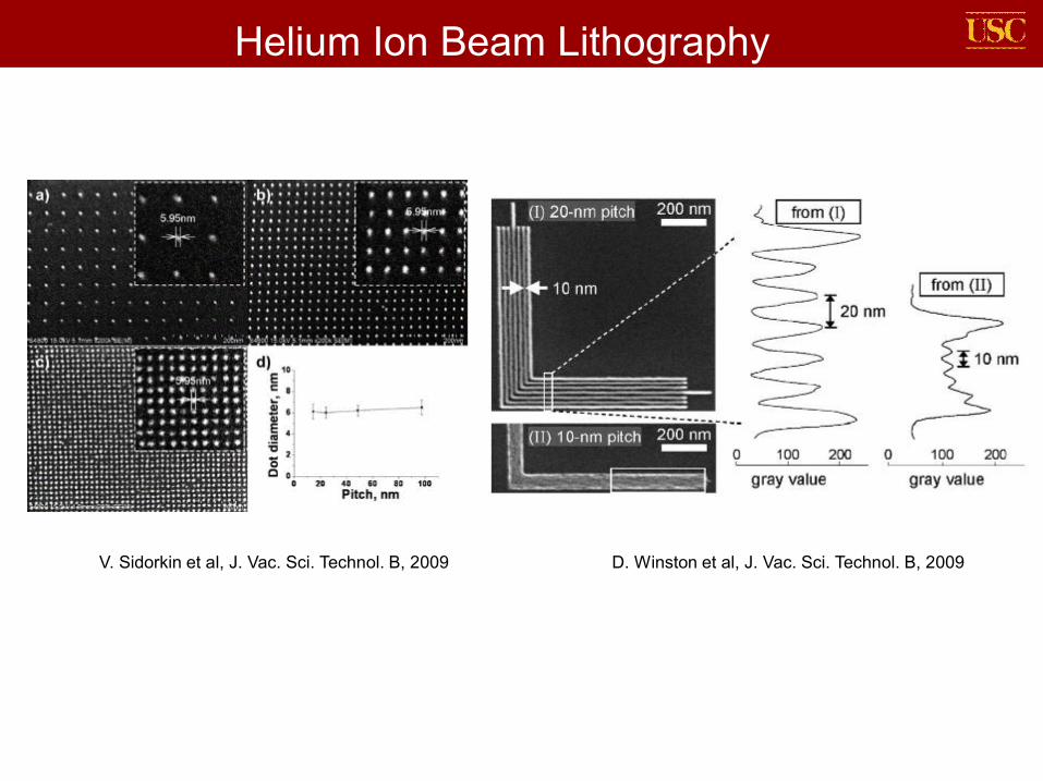
D. Winston et al, J. Vac. Sci. Technol. B, 2009V. Sidorkin et al, J. Vac. Sci. Technol. B, 2009
Helium Ion Beam Lithography
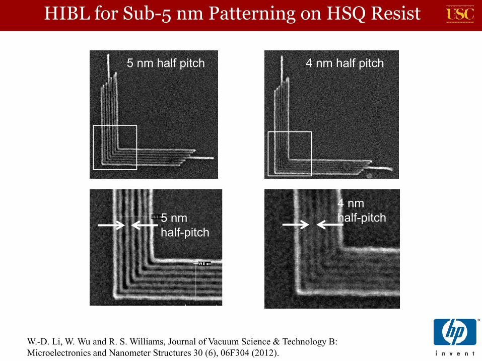
HIBL for Sub-5 nm Patterning on HSQ Resist
5 nm half pitch 4 nm half pitch
5 nm half-pitch
4 nm half-pitch
W.-D. Li, W. Wu and R. S. Williams, Journal of Vacuum Science & Technology B: Microelectronics and Nanometer Structures 30 (6), 06F304 (2012).
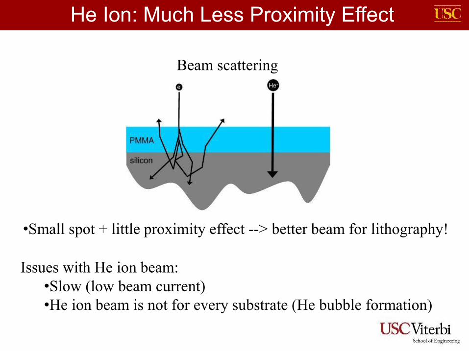
He Ion: Much Less Proximity Effect
Beam scattering
•Small spot + little proximity effect --> better beam for lithography!
Issues with He ion beam:•Slow (low beam current)•He ion beam is not for every substrate (He bubble formation)
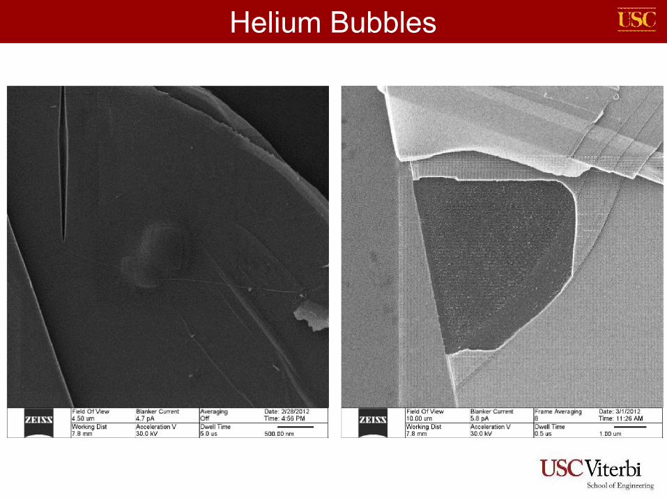
Helium Bubbles
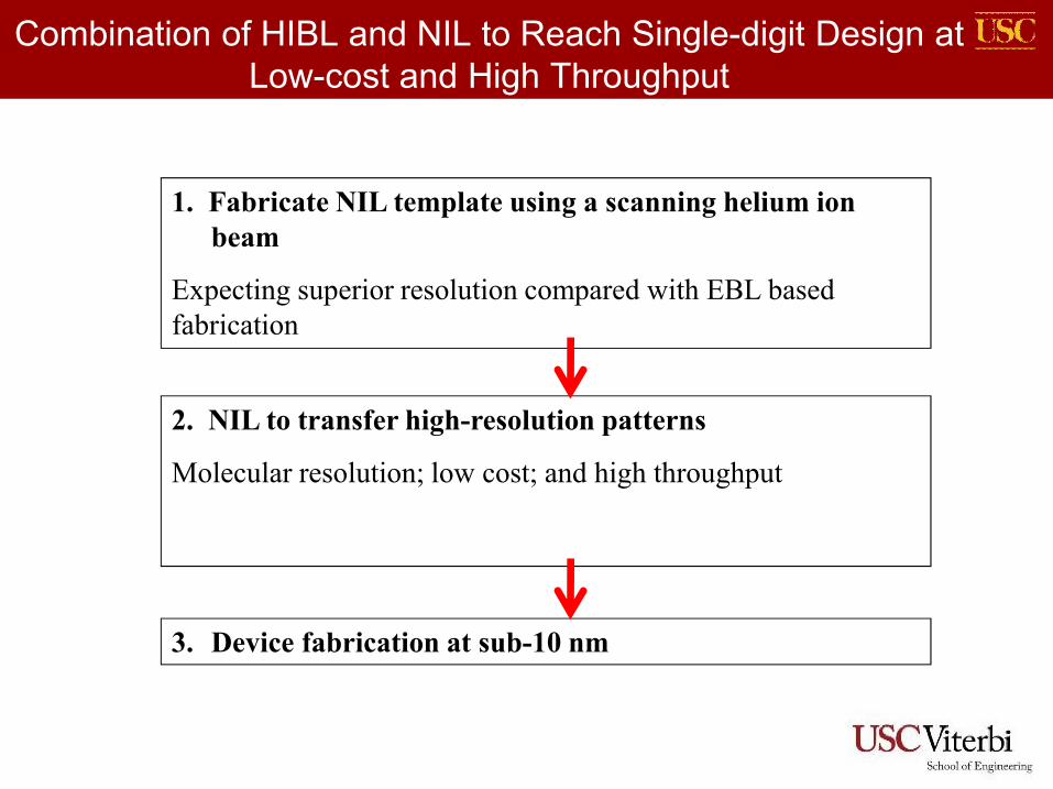
Combination of HIBL and NIL to Reach Single-digit Design at Low-cost and High Throughput
1. Fabricate NIL template using a scanning helium ion beam
Expecting superior resolution compared with EBL based fabrication
2. NIL to transfer high-resolution patterns
Molecular resolution; low cost; and high throughput
3. Device fabrication at sub-10 nm
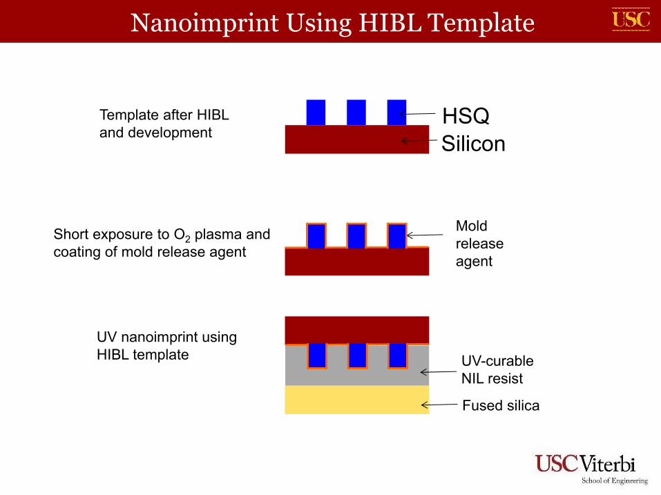
Nanoimprint Using HIBL Template
HSQSilicon
Template after HIBL and development
Short exposure to O2 plasma and coating of mold release agent
Mold release agent
UV-curable NIL resist
Fused silica
UV nanoimprint using HIBL template
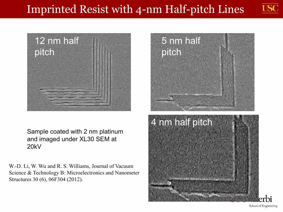
Imprinted Resist with 4-nm Half-pitch Lines
12 nm half pitch
5 nm half pitch
4 nm half pitchSample coated with 2 nm platinumand imaged under XL30 SEM at 20kV
W.-D. Li, W. Wu and R. S. Williams, Journal of Vacuum Science & Technology B: Microelectronics and Nanometer Structures 30 (6), 06F304 (2012).
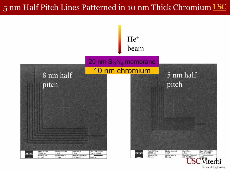
5 nm Half Pitch Lines Patterned in 10 nm Thick Chromium
5 nm half pitch
8 nm half pitch
20 nm Si3N4 membrane
10 nm chromium
He+
beam

Nanoimprint of 3D Patterns
W. Wu, M. Hu, F. S. Ou, Z. Y. Li and R. S. Williams, Nanotechnology 21 (25), -(2010)
Si polymer with Au
• NIL duplicates 3-D nanostructures into a transparent UV-cured polymer
• High aspect ratio and resolution patterning (<10 nm in tip radius, ~ 2 mm in height)
• Si master is fabricated Bosch etching process
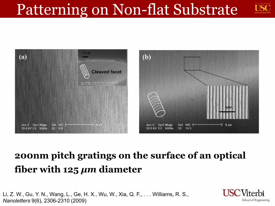
Patterning on Non-flat Substrate
200nm pitch gratings on the surface of an optical
fiber with 125 μm diameter
Li, Z. W., Gu, Y. N., Wang, L., Ge, H. X., Wu, W., Xia, Q. F., . . . Williams, R. S., Nanoletters 9(6), 2306-2310 (2009)
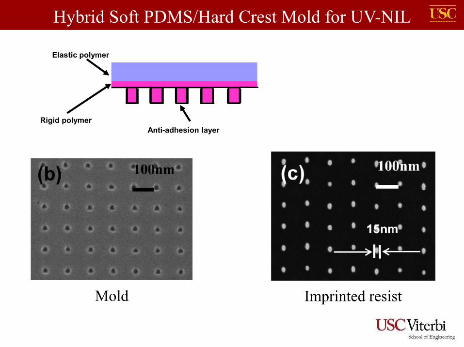
Rigid polymer
Elastic polymer
Anti-adhesion layer
Hybrid Soft PDMS/Hard Crest Mold for UV-NIL
Mold Imprinted resist
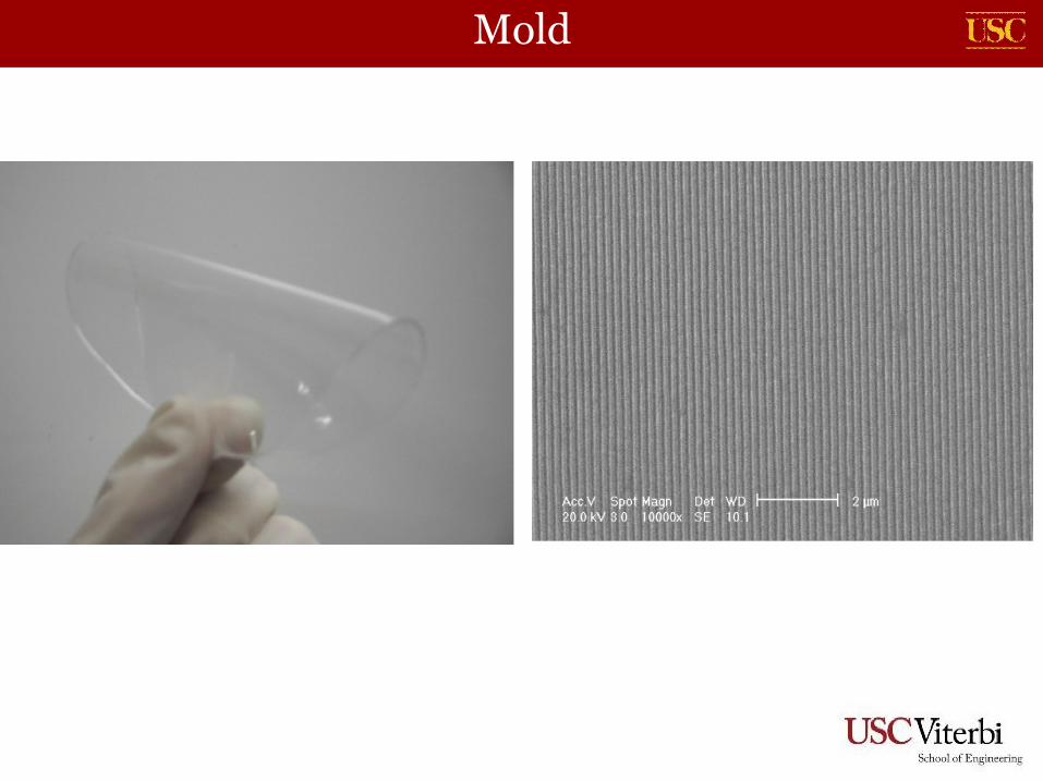
Mold
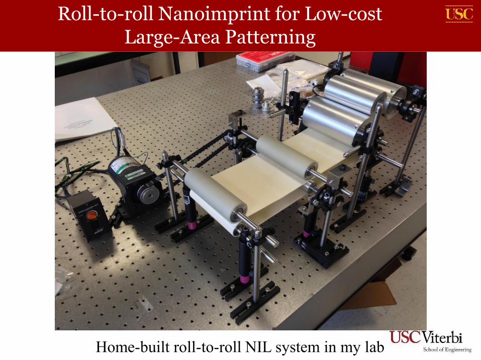
Roll-to-roll Nanoimprint for Low-cost Large-Area Patterning
Home-built roll-to-roll NIL system in my lab
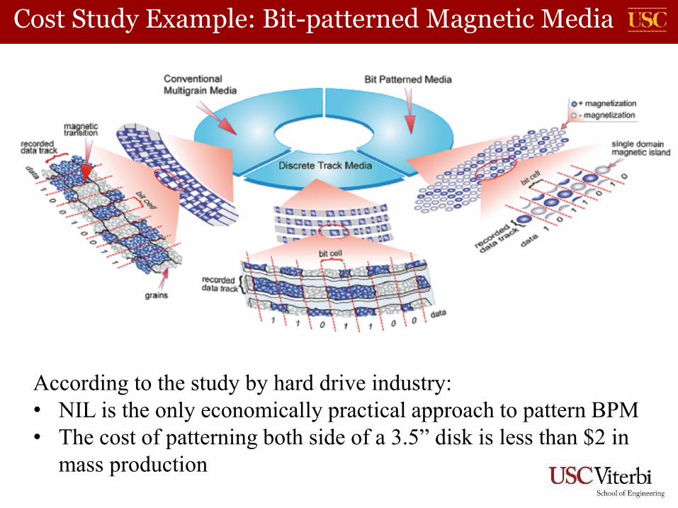
Cost Study Example: Bit-patterned Magnetic Media
According to the study by hard drive industry:• NIL is the only economically practical approach to pattern BPM• The cost of patterning both side of a 3.5” disk is less than $2 in
mass production
Nano-crossbar Circuits
Color Reflective Display Based on Nanophotonics
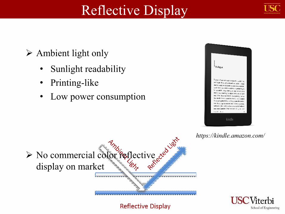
Ambient light only
Reflective Display
https://kindle.amazon.com/
• Sunlight readability
• Printing-like
• Low power consumption
No commercial color reflective display on market
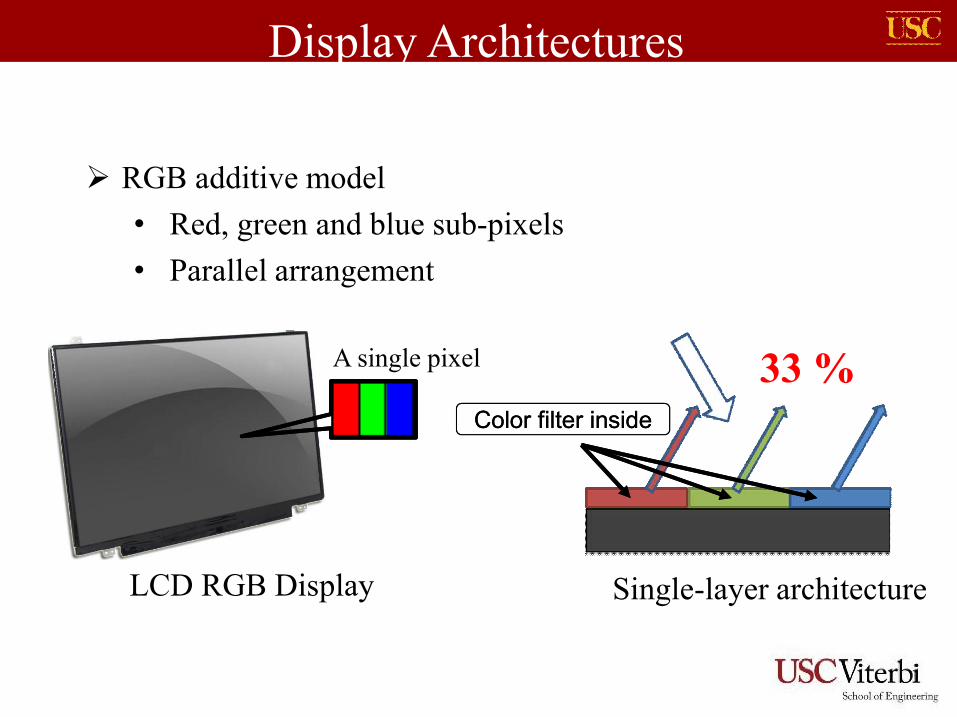
Single-layer architecture
Color filter insideColor filter inside
Display Architectures
RGB additive model
• Red, green and blue sub-pixels
• Parallel arrangement
LCD RGB Display
A single pixel 33 %
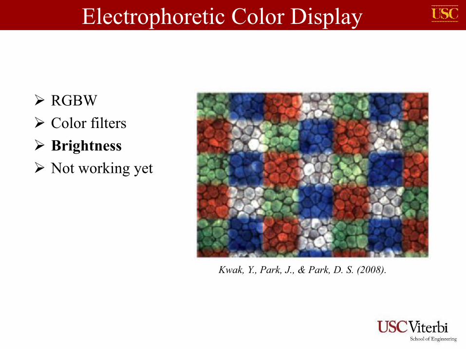
RGBW
Color filters
Brightness
Not working yet
Electrophoretic Color Display
Kwak, Y., Park, J., & Park, D. S. (2008).
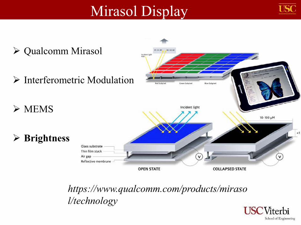
Qualcomm Mirasol
Interferometric Modulation
MEMS
Brightness
Mirasol Display
https://www.qualcomm.com/products/mirasol/technology
Stack Architectures
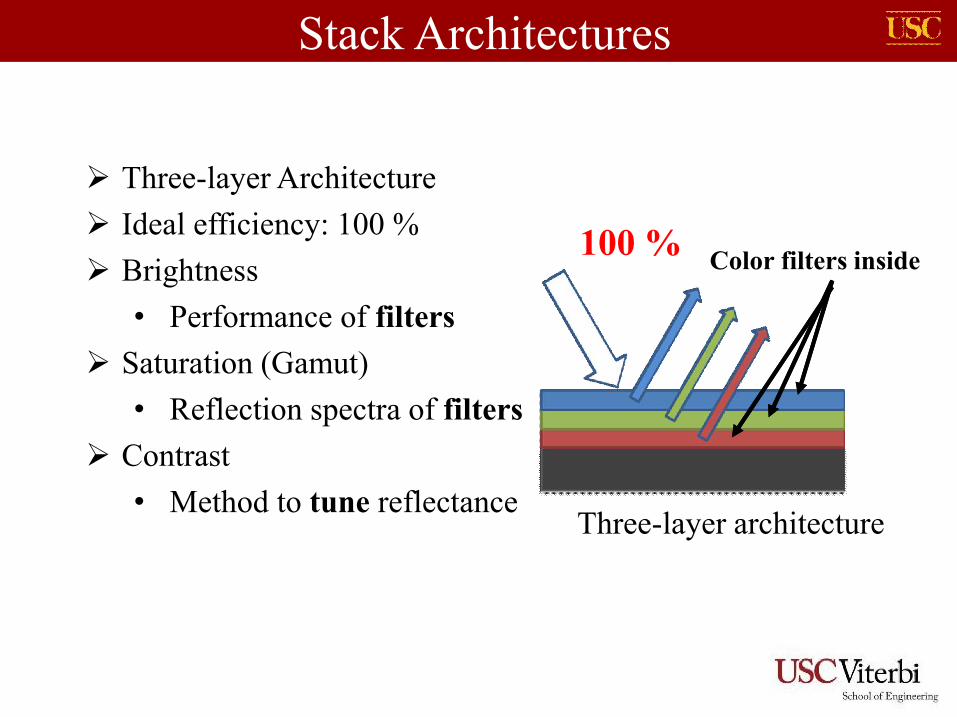
Three-layer Architecture
Ideal efficiency: 100 %
Brightness
• Performance of filters
Saturation (Gamut)
• Reflection spectra of filters
Contrast
• Method to tune reflectanceThree-layer architecture
Color filters inside100 %
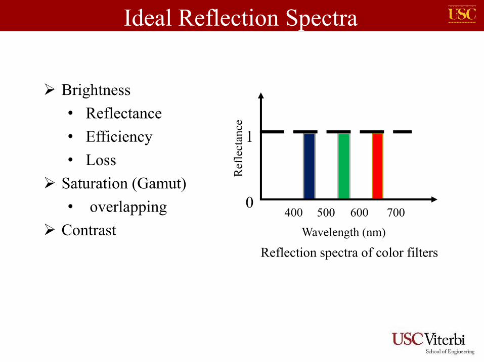
Ideal Reflection Spectra
Brightness
• Reflectance
• Efficiency
• Loss
Saturation (Gamut)
• overlapping
Contrast
1
0400 500 600 700
Wavelength (nm)R
efle
ctan
ce
Reflection spectra of color filters
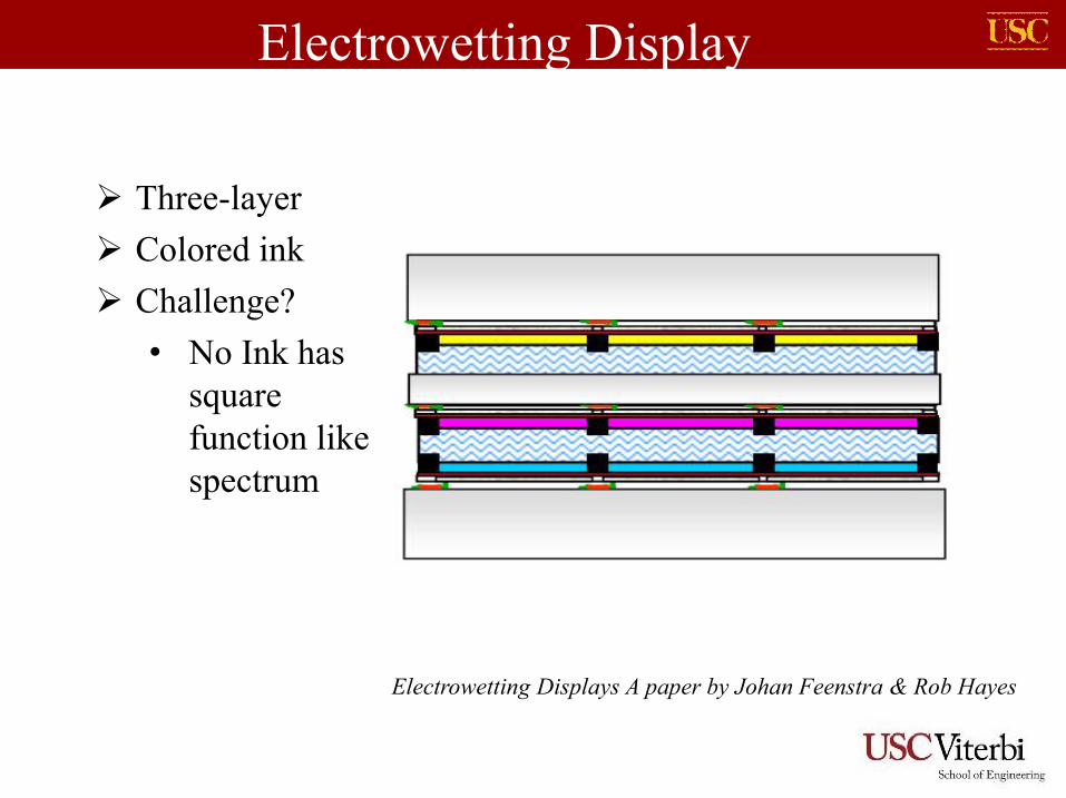
Three-layer
Colored ink
Challenge?
• No Ink hassquarefunction likespectrum
Electrowetting Display
Electrowetting Displays A paper by Johan Feenstra & Rob Hayes
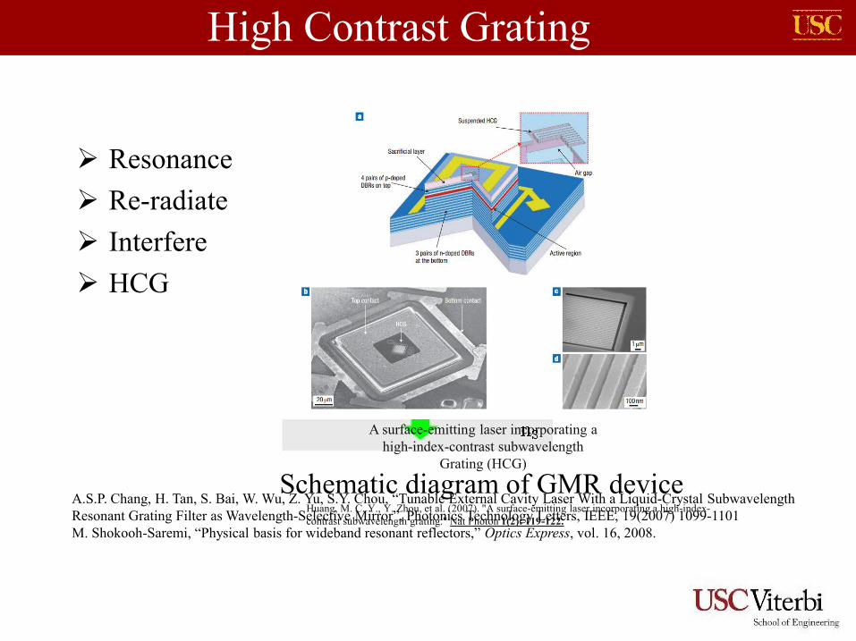
High Contrast Grating
Resonance
Re-radiate
Interfere
HCG
A.S.P. Chang, H. Tan, S. Bai, W. Wu, Z. Yu, S.Y. Chou, “Tunable External Cavity Laser With a Liquid-Crystal SubwavelengthResonant Grating Filter as Wavelength-Selective Mirror”, Photonics Technology Letters, IEEE, 19(2007) 1099-1101M. Shokooh-Saremi, “Physical basis for wideband resonant reflectors,” Optics Express, vol. 16, 2008.
Schematic diagram of GMR device
A surface-emitting laser incorporating ahigh-index-contrast subwavelength
Grating (HCG)
Huang, M. C. Y., Y. Zhou, et al. (2007). "A surface-emitting laser incorporating a high-index-contrast subwavelength grating." Nat Photon 1(2): 119-122.
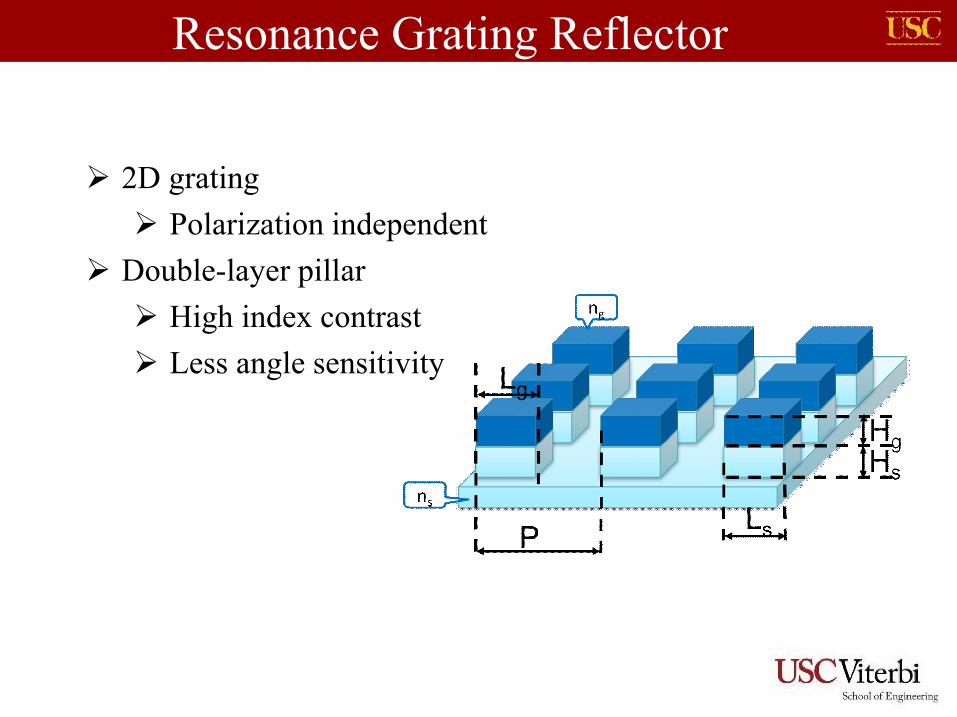
Resonance Grating Reflector
2D grating
Polarization independent
Double-layer pillar
High index contrast
Less angle sensitivity
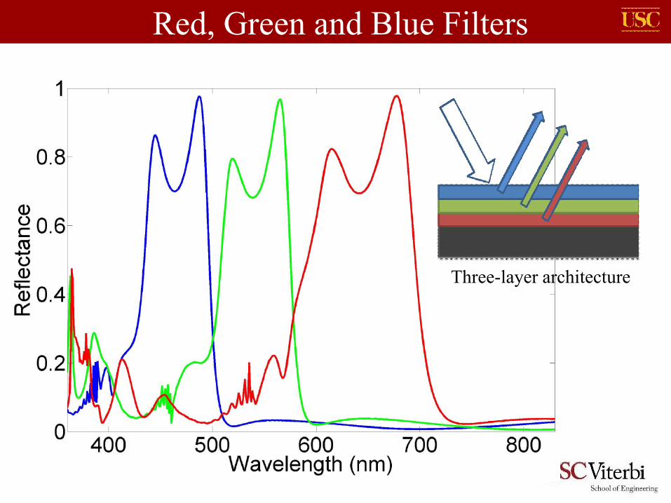
Red, Green and Blue Filters
Three-layer architecture
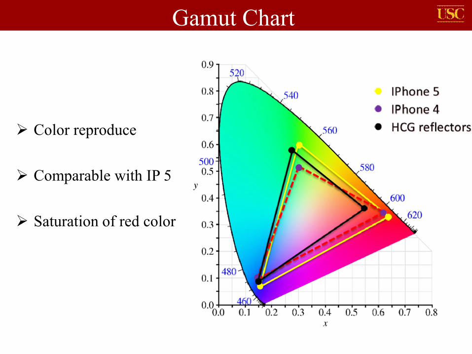
Gamut Chart
Color reproduce
Comparable with IP 5
Saturation of red color
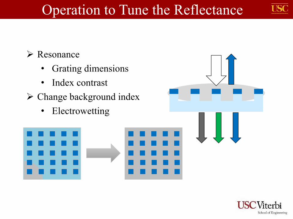
Resonance
• Grating dimensions
• Index contrast
Change background index
• Electrowetting
Operation to Tune the Reflectance
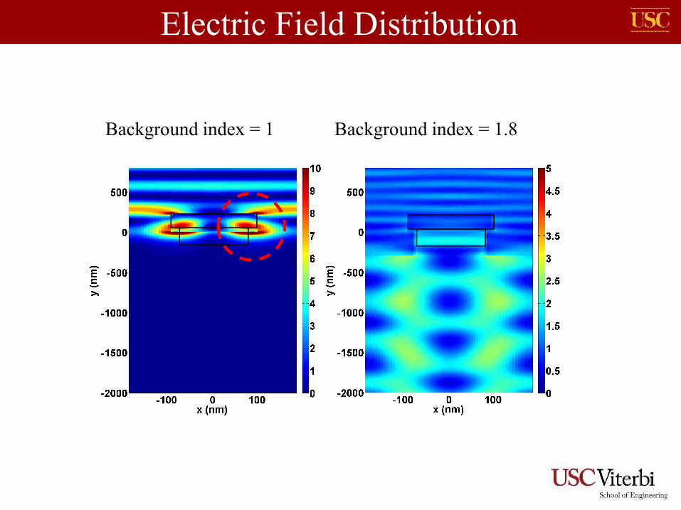
Electric Field Distribution
Background index = 1 Background index = 1.8
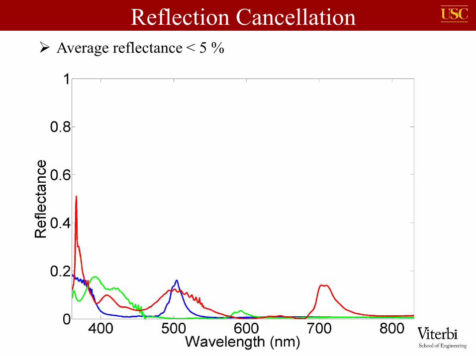
Reflection Cancellation Average reflectance < 5 %
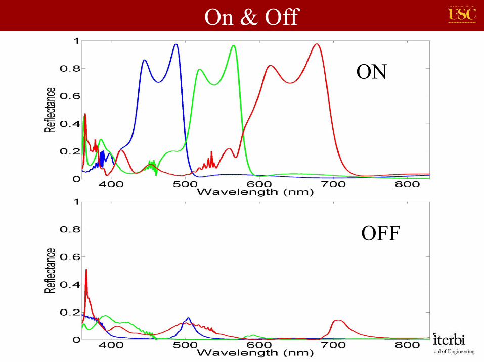
On & Off
ON
OFF

Reflection vs Background Index
Water1.32
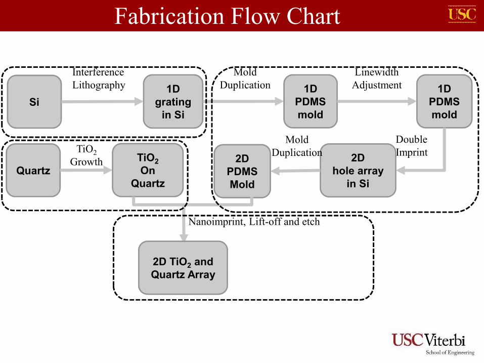
1D grating
in Si
1D PDMS mold
1D PDMS mold
2D hole array
in Si
Si
Interference Lithography
MoldDuplication
LinewidthAdjustment
2D PDMS Mold
MoldDuplication
QuartzTiO2
On Quartz
TiO2
Growth
DoubleImprint
Nanoimprint, Lift-off and etch
2D TiO2 and Quartz Array
Fabrication Flow Chart
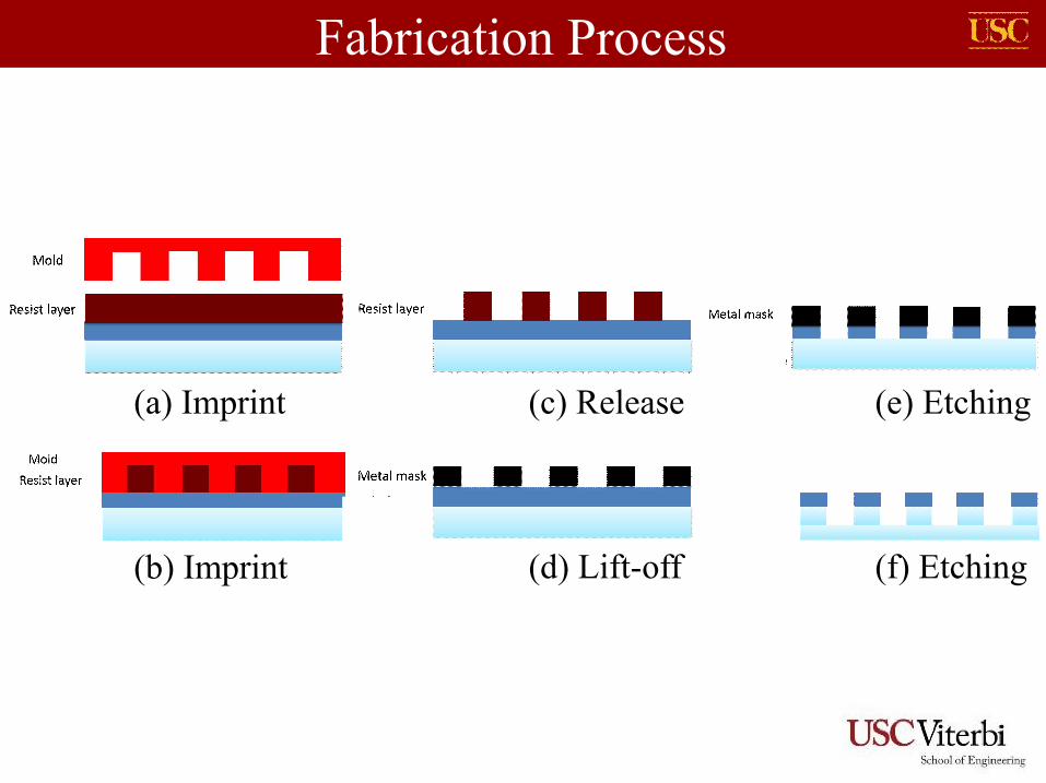
Fabrication Process
(a) Imprint (c) Release (e) Etching
(b) Imprint (d) Lift-off (f) Etching
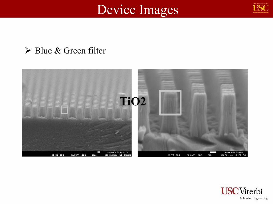
Device Images
Blue & Green filter
TiO2
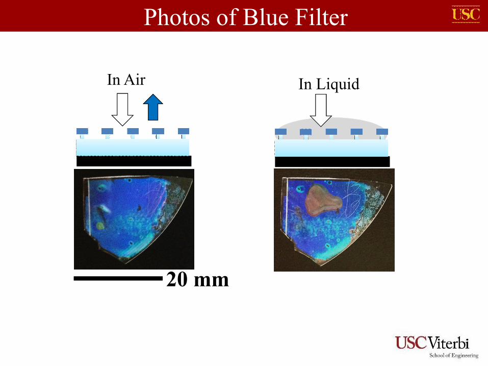
Photos of Blue Filter
20 mm
In Air In Liquid
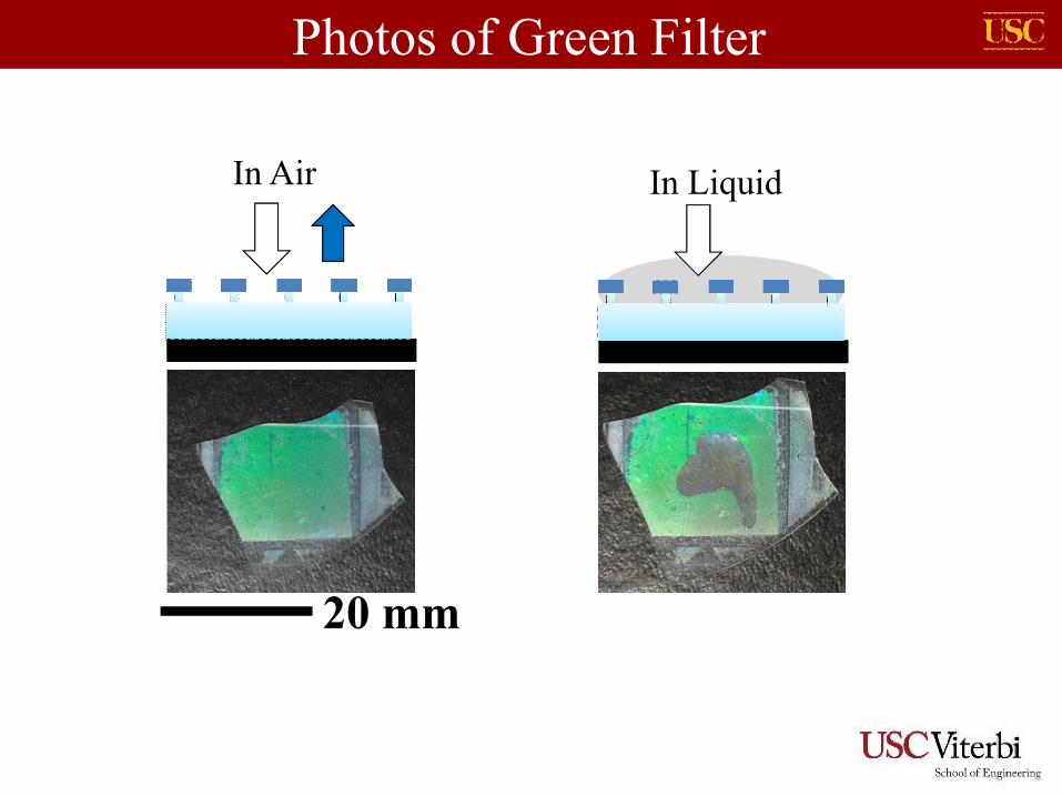
Photos of Green Filter
20 mm
In Air In Liquid
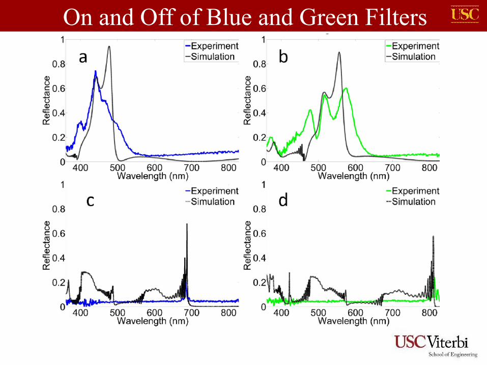
On and Off of Blue and Green Filters
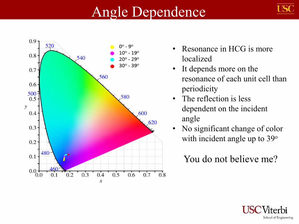
Angle Dependence
• Resonance in HCG is more localized
• It depends more on the resonance of each unit cell than periodicity
• The reflection is less dependent on the incident angle
• No significant change of color with incident angle up to 39o
You do not believe me?
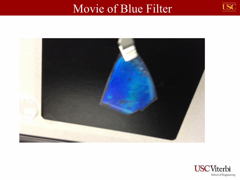
Movie of Blue Filter
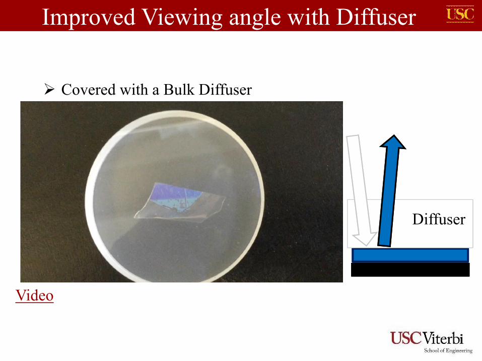
Improved Viewing angle with Diffuser
Covered with a Bulk Diffuser
Diffuser
Video
Important specification
Grating Unit Counts
Optical Localization
Resolution
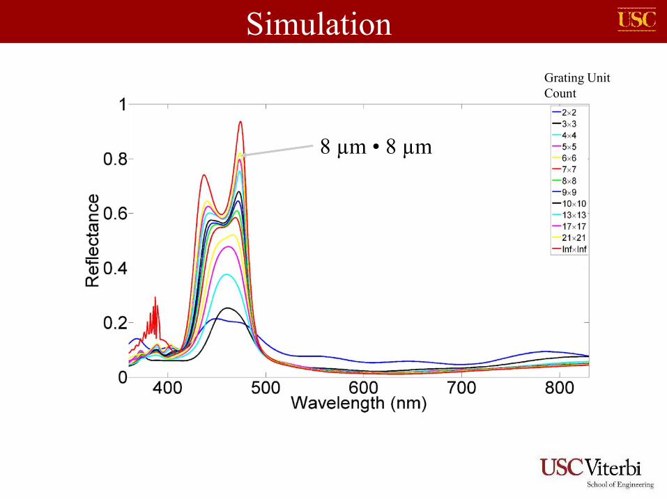
Simulation
8 µm • 8 µm
Grating UnitCount
Resolution
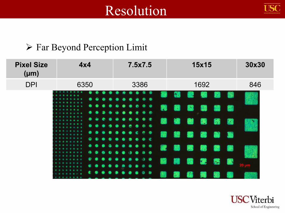
Far Beyond Perception Limit
Pixel Size(µm)
4x4 7.5x7.5 15x15 30x30
DPI 6350 3386 1692 846
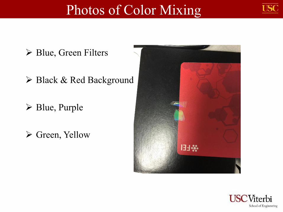
Photos of Color Mixing
Blue, Green Filters
Black & Red Background
Blue, Purple
Green, Yellow
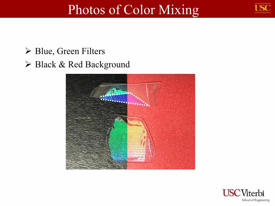
Photos of Color Mixing
Blue, Green Filters
Black & Red Background
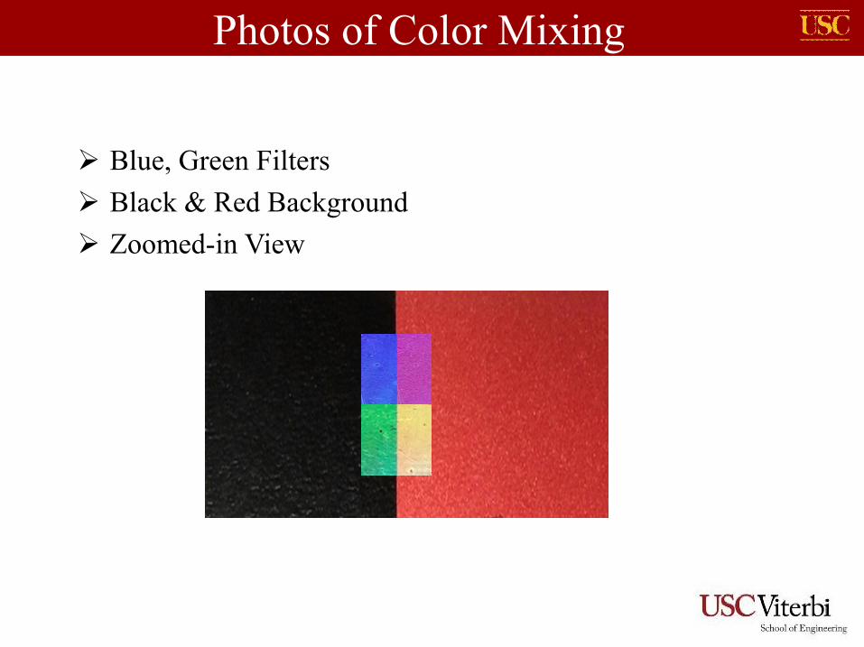
Photos of Color Mixing
Blue, Green Filters
Black & Red Background
Zoomed-in View
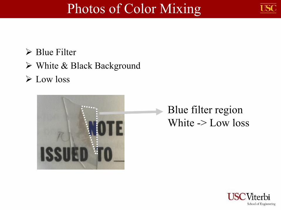
Photos of Color Mixing
Blue Filter
White & Black Background
Low loss
Blue filter regionWhite -> Low loss
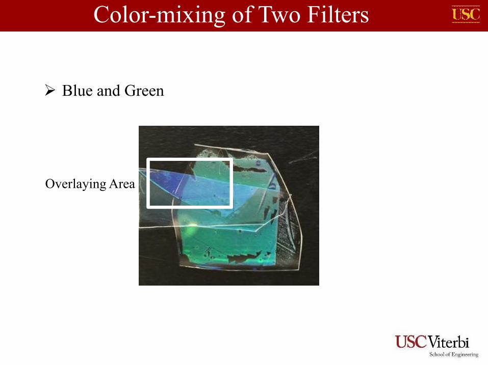
Color-mixing of Two Filters
Blue and Green
Overlaying Area
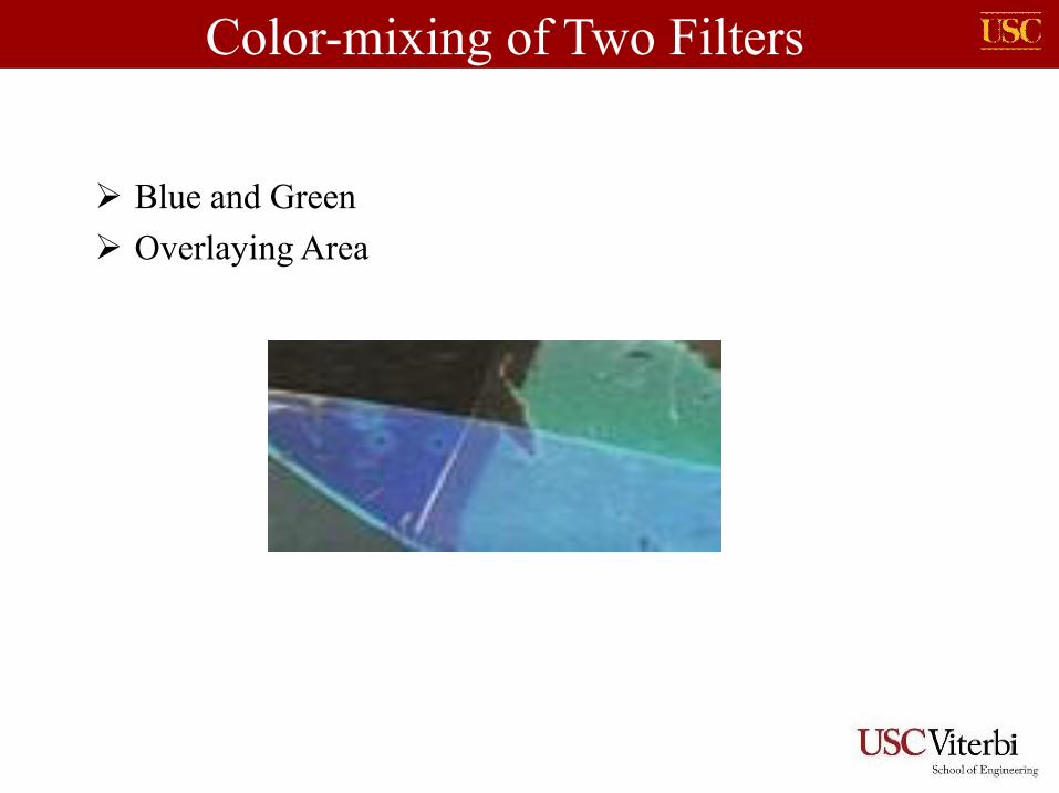
Color-mixing of Two Filters
Blue and Green
Overlaying Area
Summary
• Nanoimprint lithography• High resolution• Low cost• Large area• 3D structure• Non conventional substrates
• Invented a color reflective display with potential forunprecedented vivid color• Developed the fabrication processes• Proved the feasibility
• Bright color• Large Viewing Angle• Colored & Clear States• High resolution• Color-mixing
• Nanoimprint has great potential beyond semiconductor
Acknowledgement
R. Stan Williams, Doug Ohlberg
Wen-Di Li
Yuhan Yao, Yifei Wang, He Liu, Yuanrui Li, Boxiang Song


![Etching of 42 nm and 32 nm Half-Pitch Features Patterned ...cnt.canon.com/wp-content/uploads/2014/07/SPIE-2008-etch-study.pdf · [Figure 1]. The authors demonstrate control of CDs,](https://img.pdfslide.net/doc/110x75/5eba3308912d953f6d5f60de/etching-of-42-nm-and-32-nm-half-pitch-features-patterned-cntcanoncomwp-contentuploads201407spie-2008-etch-studypdf.jpg)