Embed Size (px)
Citation preview
HAL Id: hal-00651636https://hal.archives-ouvertes.fr/hal-00651636
Submitted on 14 Dec 2011
HAL is a multi-disciplinary open accessarchive for the deposit and dissemination of sci-entific research documents, whether they are pub-lished or not. The documents may come fromteaching and research institutions in France orabroad, or from public or private research centers.
L’archive ouverte pluridisciplinaire HAL, estdestinée au dépôt et à la diffusion de documentsscientifiques de niveau recherche, publiés ou non,émanant des établissements d’enseignement et derecherche français ou étrangers, des laboratoirespublics ou privés.
Nanoscience with non-equilibrium plasmas atatmospheric pressure
T Belmonte, G Arnoult, G Henrion, T Gries
To cite this version:T Belmonte, G Arnoult, G Henrion, T Gries. Nanoscience with non-equilibrium plasmas at atmo-spheric pressure. Journal of Physics D: Applied Physics, IOP Publishing, 2011, 44 (36), pp.363001.�10.1088/0022-3727/44/36/363001�. �hal-00651636�

1
NANOSCIENCE WITH NON-EQUILIBRIUM PLASMAS AT
ATMOSPHERIC PRESSURE
T Belmonte* G Arnoult G Henrion T Gries
Institut Jean Lamour, Department of Chemistry and Physics of Solids and Surfaces, Nancy-
Université, CNRS, Parc deSaurupt, CS 14234, F-54042 Nancy Cedex, France
* Corresponding author
Fax : +33 3 83 53 47 64
E-mail : [email protected]
PACS number: 81.16.-c Methods of nanofabrication and processing
52.77.-j Plasmaapplications
Keywords: atmospheric pressureplasma ; microplasma ; nanoscience
Confidential: not for distribution. Submitted to IOP Publishing for peer review 10 June 2011

2
Abstract
This review devoted to nanoscience with atmospheric pressure plasmas shows how
nanomaterials are synthesised locally using three main ways: localized PECVD, nanoparticles
and templates. On the other hand, self-organization of nano-objects on surfaces is driven by
electric fields, stress and high temperatures. We show that the specificities of plasmas at high
pressure, as their small size, their self-organization or their filamentation have been little
exploited in thesynthesis of nanomaterials. Finally, perspectives in the field are given.
3
1. Introduction
After the development of micro-discharges that resulted from the renewed interest in plasmas
generated at atmospheric pressure, many attempts were made to grow nanostructures on
surfaces without vacuum [1-5]. The first nanostructures were built by mimicking the methods
adopted to grow carbon nanotubes under vacuum [6-10]. These original approaches consisted
in utilizing atmospheric plasmas that are much easier to implement on industrial production
lines in order to reproduce results obtained in low-pressure conditions.
The development of micro-plasmas has strongly contributed in reorienting works towards
applications where a localized treatment is necessary. One of the best example is certainly
plasma treatment for biomedical applications where the possibility to operate at atmospheric
pressureopens up new perspectives [11-16].
Treatments at atmospheric pressure have specific characteristics. For example, cold plasmas
at atmospheric pressure differ from cold plasmas under vacuum by weak laminar diffusion
fluxes that are most often negligible compared to other fluxes of transfer of matter. Increasing
the pressure gives rise spontaneously to plasma filaments of small dimensions [17-20]. Then,
plasmas at atmospheric pressure have features that cannot be found in low-pressure plasmas.
We shall endeavour to illustrate how these features can be advantageously used in the field of
nanoscienceand nanotechnology.
Several important topical reviews [21-34] were proposed over the last decade to give brilliant
overviews of plasma nanoscience. Some focussed on specific materials like carbon and its
various forms [21, 22, 24, 29] or semi-conductor nanocrystals [28]. Ostrikov et al.
emphasized the specificity not only of low-pressure plasmas [23, 25-27, 32-34] but also of
thermal plasmas [26]. Finally, two excellent papers written by Mariotti and Sankaran [30, 35]
discuss some features of microplasmas for nanomaterials synthesis. The present review aims

4
to complete these works and more specifically the last ones by detainling strategies to grow
nanostructures with non-equilibrium plasmas at atmospheric pressure.
In this work, we introduce two general approaches. In the first one, self-organized
nanostructures grow on surfaces as parts of a coating deposited at larger scale by plasma.
Such an approach was first proposed under vacuum [26-39], and more recently at atmospheric
pressure [40-43]. Matter gets organized spontaneously on the substrate and, under the effect
of the plasma, produces architectures of nanometric objects. In the second approach, the
possibility to grow an isolated nanometric object from atmospheric plasmas and eventually to
assemble several of these elementary units into given architectures was described by several
groups [44-47], with modest, yet undeniable, success. To date, all the achievements made
with this second approach are micrometric, but recent developments on plasmas in or on
liquids [48] suggest that it would be possible to reach the nanometre scale. Indeed, liquid
interfaces or media could be used to scale down processes where cold plasmas at atmospheric
pressure already allows experimentalists to synthesise micrometric objects. For example, it is
possible to determine locally, i.e. over distances limited to several hundreds of nanometres,
thecomposition of a liquid by creating aplasma with ananotube electrodeand by observing it
by optical emission spectroscopy [49].
We propose to establish an overview of the state-of-the-art nanoscience based on cold
plasmas at atmospheric pressure. This article is structured as follows. In section 2, we present
a general overview of the different plasma sources used in the two approaches described
previously for growing nanostructures on a surface. In section 3, we describe the three ways
that are adopted to grow an isolated nanometric object on a surface. In section 4, we discuss
two main ways to get self-organized nanostructures. The article concludes with a summary of
themain challenges ahead and theoutlook for the future research in the field.
2. Plasma sources at atmospheric pressure for nanostructures

5
Plasma sources used to grow nanostructures are very heterogeneous in terms of gas
temperature, electron temperature, active species density, etc. Categorising them is not an
easy task. Roughly, we can distinguish three types of sources: Large Area Dielectric Barrier
Discharges, Microplasma jets and plasma torches. This presentation suffers from a lack of
consistency since specificities of each type of sources can be found in another type. For
example, microplasma jets can be dielectric barrier discharges. However, this classification is
generally adopted by the authors themselves and it will be kept here on purpose. Indeed, we
shall not review in this part the physics of these sources which can be found elsewhere (for
dielectric barrier discharges, see [1, 50, 51] ; for microplasma jets, see [2, 6, 52, 53] ; for
plasma torches see [54] ; and [55] for a general overview). We shall give only the main
specificities that are looked for when onewishes to use thesesources in nanoscience.
2.1. Large Area Dielectric Barriers Discharges
Dielectric Barrier Discharges are low temperature plasmas that can be used to treat large
areas. A DBD device consists of two parallel metal electrodes, at least one of which being
covered by a dielectric layer (figure 1a – after Jiang et al. [44]). To ensure stable operation,
the gap which separates the electrodes is limited to a few millimetres wide. The discharge is
sustained by a sinusoidal or a pulsed electric field. Depending on the composition of the
working gas, the voltage and the frequency excitation, the discharge can be either filamentary
or glow. A filamentary discharge is a set of micro-discharges or streamers more or less
randomly distributed over the dielectric surface. One key issue of Dielectric Barrier
Discharges used for material processing is the distribution of these streamers as a function of
time. Different mechanisms were identified showing that preferential conditions can be
encountered to reignite a streamer on a spot just hit by a previous streamer. For instance,
periodic patterns like hexagon structure and stripe structure have been observed in DBD due
to short-range interactions between streamers. The non-uniformity caused by the filamentary

6
nature of the discharge can be turned into an advantage as described later. However, no self-
organized pattern of streamers was used for nanosciencepurposes.
Important efforts were made to produce atmospheric pressure glow discharges. However,
special conditions must be fulfilled to get a homogenous discharge like the addition of helium
or nitrogen in the discharge and the use of millimetre gaps. Basically, the avalanche-to-
streamer transition can be avoided by increasing the avalanche radius and by providing
sufficient pre-ionization [56]. Helium and nitrogen are gases which favour this phenomenon
and therefore, glow discharges. These glow discharges, as such, have been used to grow
carbon nanotubes [57] and silicon nanoparticles [58]. Associated with cyclone system, they
can be run to coat particles [59, 60]. They are certainly used by default in DBD microplasma
jets where gaps areextremely small (down to 100 µm).
The electron density of atmospheric pressure glow discharges lies between 109 and 1013 cm−3.
In non-uniform discharges, it lies rather between 1014 and 1015 cm−3. To increase the plasma
density, “pin-to-plate” arrangements and dielectric barrier with capillary holes were proposed
(figure 1b-e). Pin-to-plate dielectric barrier discharges [61] are composed of a multi-pin
power electrode. Such sources were developed to generate high density plasmas with low
breakdown voltage [62]. The pin shape enhances the applied local electric field. Substrates
can be processed in direct plasma (figure 1b after [63]). However, to avoid the non-uniformity
caused by the filamentary nature of the discharge, another source was designed to operate in
the remote mode [64]. In this case, the power electrode is made of aluminium and machined
to have multi-pins with a pyramid shape, as shown in figure 1c (after [65]). Electrodes are
coated with 300 µm thick alumina to have the dielectric barrier. Another solution was
proposed by Kyung et al. [66]. A dielectric barrier with capillary holes was preferred (figure
1d) to get a more uniform reactive gas distribution compared to conventional dielectric barrier
discharges. It also produces a higher plasma density due to ion-beam like plasmas created in

7
holes. Another configuration based on the same idea was proposed by Jiang et al. [67] (figure
1e). A grid electrode made of stainless steel, much easier to machine than the dielectric
material, is placed between the dielectric barrier and the substrate. It turns out that high
density plasmas with high uniformity areusually preferred to grow nanostructures.
2.2. Microplasma jets
Microplasma jets can be created by any excitation mode (dc [68], rf [45], microwave [46,
47]). They can be processed directly or in a remote mode, continuously or in a pulsed regime.
Basically, a low total energy is deposited into a localized small space, making possible the
control of the heat flux, a necessary condition to fulfil to preserve the materials integrity. A
fine plasma jet at high temperature but with low total energy can be created. This principle
rules the behaviour of the microplasma jets that differ strongly from plasma torches where the
local thermodynamic equilibrium prevails.
Three important items concerning microplasma jets have to beaddressed:
- theuseof a capillary to localize the flow of at least oneprecursor,
- theuseof wires as consumablesources of matter,
- theexcitation mode(dc, rf, microwave) and the way the electric field is applied, which
may influence the growth of nano-objects.
The first point deals with the location of one of the two reactive precursors through
capillaries. Currently, most methods based on the use of capillaries can locate the deposition
area over a few thousands of square micrometers (the distribution in thickness generally
encountered is Gaussian and its full width at half maximum gives the diameter of the
deposition area). Capillaries are obtained by pulling a micropipette commonly made of fused
silica. When the inner diameter of the capillary is reduced, the total gas flow must be adapted
to avoid astrong increase in theupstream pressure.

8
Resorting to consumable wires can be seen as a way to synthesise vapours or nanoparticles
that are the precursors of the nanostructures to be built. In that sense, any reactive plasma
used as a source of nanoparticles plays the same role. One of the most explicit examples
based on this idea was first proposed by Ito and Terashima [69] and by Shimizu et al. during
the following years [46, 47, 70-72]. The microplasma generator consists of a capillary (100–
500 µm inner diameter) made of quartz or alumina [72] joined to a metal tube where the gases
are injected, and a tungsten wire (50 µm in diameter) inserted into the capillary. This capillary
is wound around by a 5-turn coil whose end is connected to a 450 MHz UHF generator (5–30
W) via a matching circuit, while the other end is grounded (figure 2a) [46]. An outer metallic
armour must be placed around the process to shield the external components from the high
frequency electric field. Plasma ignition is ensured by a 15 kV dc power supply. This original
idea underwent several successive changes. The previous setup was first modified with a
pinched nozzle (60–70 µm exit inner diameter) made by pulling the quartz capillary [70, 72]
(figure 2b). A 20-turn coil made of Cu wire (280 µm in diameter) was preferred to the
previous 5-turn coil. The tungsten wire was replaced by other metallic wires (50 µm in
diameter). The choice of the metal is mainly defined by the possibility to get a volatile oxide
at the temperature of the neutral species in the plasma. It is defined by the total gas flow rate
and the plasma power [73]. This strong link between plasma conditions and production of the
source material of the nanostructures is probably the biggest drawback. The problem of the
consumption of the wire could be circumvented by using a mechanism to feed the wire
continuously.
The last point deals with the excitation mode and the way the electric field is applied. Using
the same example, we notice that the distance between the substrate and the wire plays an
essential role on the final morphology of the nanostructures. This distance changes with time
because the wire is consumed. As shown in reference [71], this consumption is not uniform.
9
The control of such a process is quite complex, although it is cheap and relatively easy to
build. The energy coupling between the power supply and the plasma depends on the way the
wire vaporizes. The influence of the emission of vapours of volatile oxides on the behaviour
of the plasma is still to be clarified. The energy coupling also depends on the way the ultra
high frequency is applied. A major modification was brought to the previous device by
Mariotti et al. [40] when they proposed to remove the coil and to apply directly the UHF
signal on a bottom glass epoxy copper plated electrode (2×2 cm2) which acts as a patch
antenna (figure 2c). The substrate is placed on top of this electrode. This modification in the
power coupling strongly influences the growth of the nanostructures. As explained latter, both
the distribution of the surface electric field and the incoming flux of species from the plasma
act on theway matter gets organized.
Ichiki et al. [16] and Kikuchi et al. [74] proposed a similar configuration with a rf-plasma
(13.56 MHz). For the formers, the plasma is generated inside a capillary (1 mm inner
diameter) by applying a 100-MHz VHF power of 200–300 W to a solenoid antenna (figure
2d). SF6 gas is added to the plasma jet ejected from an annular nozzle (100-µm inner
diameter) to produce a high-density etchant flux to the sample surface. For the latters, a
needle capillary electrode, made of tungsten carbide (2 cm in length and a minimum inner
hole diameter of 150 µm) is used as rf-power electrode (figure 2e). This choice influences the
energy coupling between the power supply and the plasma. Losses of electrons and negatively
charged species at the wall of the needle electrode are described as being the main mechanism
that limits the energy transfer. The excitation temperature increases when these losses
increase. Consequently, no plasma can be sustained as soon as the oxygen concentration in
helium exceeds 5%. From a practical standpoint, it is convenient to work with microwaves
instead of radio-frequency, more difficult to implement to get a stable power matching. It
would be certainly possible to use "strip" technology [75-78] to deposit on lines instead of

10
spots. However, since erosion of the strips has always been presented as being negligible [77-
79], thestrips could not beused as a consumable material for deposition.
Among other important plasma sources, microplasmas constitutes a promising way to
synthesise nanoparticles when they are used as component of an electric circuit where charge
conduction occurs through a liquid [30, 80]. Basically, the experimental set-up contains a DC
power supply, a ballast resistance, a metal anode immersed in a conductive liquid (deionized
water with diluted acid) and a microplasma, acting as a cathode, and located 1-2 mm above
the surface of the liquid (figure 3). Synthesis of nanoparticles is explained as follows.
Dissolution of the anode produces metal cations that are transported to the anode where they
areneutralised and agglomerate to producenanoparticles.
2.3. Plasma torches
Plasma torches and micro-torches are used principally to grow nanoparticles. They can be
excited by microwave power supplies (figure 4a) [81-88] or by dc generators (figure 4b and
4c) [89-94]. Cathodic arc is mostly employed for powder synthesis whereas anodic arc is
employed for synthesis of carbon nanostructures [92-96], with a few exceptions [97]. Indeed,
anodic arc is characterized by primary anode ablation during the arc process in contrast to
cathodic arc in which cathode ablation prevails. When anodic arc is implemented for carbon
nanotube synthesis it is supported by ablation of the anode material and substantial part of the
ablated material is deposited on thecathode.
rf excitation is commonly found in thermal plasmas [26, 98-102] to grow nanoparticles. The
so-called rf induction thermal plasma (figure 4d) offers longer residence times, because of
large plasma volume and low gas velocities. Furthermore, as for microwave sources, rf
torches arecontamination freebecause it can be generated without any internal electrodes.
The main issued attached to the synthesis of nanoparticles in atmospheric plasmas are the
following ones:
11
- Control of the purity (high quality gases, no vapour release from the walls, no leak
flow, etc.)
- Control of the modal and size distributions of the particles, and consequently, the
electric charges carried by thesenanoparticles.
- Avoid theaggregation into clusters
- Production of core-shell and alloy nanoparticles
In regards to theory, we can also add the need to model accurately the growth of nanoparticles
in thermal plasmasynthesis.
The supersaturation of species in the vapour phase is the driving force for particle
condensation, resulting in the production of ultrafine particles by homogeneous nucleation. In
any process of powder synthesis, the plasma torch is only one part of a more complex layout
in which it is associated with other devices. A quenching section improves strongly the
product quality (figure4b). By varying thequenching gas flow in this section, thewidth of the
particle size distribution can be reduced significantly. The main difference between
unquenched and quenched products is found in the tail on the large particle side of the size
distribution. The size distribution of the largest part of the particles is hardly affected [103].
Next, a collector is needed to extract particles from the gas phase. Finally, process gases can
be recirculated but this step usually affects thepurity of the gases with process time.
Atmospheric pressure plasma torches are fed by a precursor which is mainly solid or liquid.
Liquid precursors are either suspensions, aqueous or organic solutions. The precursor is
admixed to the system either axially, the inner electrode playing the role of a nozzle, or
outside the electrode system, perpendicularly to the plasma torch (figure 4c). The former
configuration is mainly used when liquid precursors are chosen and care must taken to avoid
clogging at the tip of the nozzledue to reaction products.
12
These plasma torches are usually at or not too far from thermal equilibrium. Temperatures are
commonly above 4000 K [104]. Since all the metals and most oxides are melted, there is no
correlation between the size distributions of the input and the output particles. Bipolar
charged particles are produced, leading to relatively broad size distribution of the output
particles.
Microwave torches are characterized by gas temperatures up to a few thousands Kelvins.
They are mainly excited at 2.45 GHz by surface guided waves [81, 83-88] or by TIA-like
structures [105-107] following the original idea of the Torche à Injection Axiale (TIA)
proposed by Moisan et al. in 1994 [108]. Sources excited by surface guided waves are useful
to treat nanoparticles, confining them in the reaction tube used to guide the waves whereas
TIA-likestructures aremoreadapted to localized treatments.
3. Isolated nanometric object
In general, using plasmas to grow isolated nanometric objects presents the major advantage to
lower the process temperature and to offer a wide range of materials that can be processed. In
particular, resorting to atmospheric plasmas not only simplifies the treatment procedures but
also give access to the treatment of fragile materials that could be damaged under vacuum,
like living materials. For industrial applications, deposition of isolated nanometric objects
could be used for direct local machining without the use of a mask [71]. With a motorized
xyz-stage, it is possible to control the location of the deposition area on the substrate
accurately and to build with these elemental units larger architectures [109]. Semiconductor
with a large band-gap that could be deposited locally would present a great potential as a gas-
sensing device [59]. The next step is to be able to grow coatings from a direct assembly of
nanoparticles. Indeed, nanostructuration of composites is known to confer extraordinary
properties to materials. New ultra-hard materials could be “designed” by these new processes
[110]. On the other hand, the possibility to deposit isolated nanometric objects could also be
13
exploited to decorate fibres for a variety of potential applications, including catalysis, sensors,
electronic devices, magnetics, optics and others [111]. Finally, 1D nanostructures grown in
templates such as nanotubes and nanowires, offer potential applications in nanodevices [112].
The synthesis of isolated objects at the micrometre scale by plasma at atmospheric pressure
takes today three main ways. The first one is based on plasma enhanced chemical vapour
deposition (PECVD) by locating the deposit on an area as small as possible. The second one
focuses on theuseof nanoparticles. The last oneuses templates.
3.1. Localized PECVD
The ability to "localize" coatings by PECVD appeared in 2001. Jiang et al. [44] use the
specificity of a filamentary Dielectric Barrier Discharge (260 torr - Ar-2.6 vol.%C2H2
mixture) to deposit an array of carbon-based columns that grow along streamers self-
organized in network. These authors mention for the first time a “ localized PECVD”. The
plasma deposition process evolves as time passes. Three steps are clearly identified. The
plasma is of the glow-type during a short period and quickly becomes filamentary, leading to
dot-like structures of 10 µm in diameter. Next, the localised growth of columns occurs from
some of the deposited dots and it compels streamers to attach on the tips of these emerging
microstructures. Thicker but fewer filaments appear progressively, attached on the highest
columns. They form, after a short transient step, an unchanging pattern. The columns (~100
µm in diameter) present naturally three different structures corresponding to each step. The
transition from one mode to another is likely due to enhancement of the electric field due to
shape effects. Columns are stacks of nanoparticles where carbon atoms with single, double
and even triple bonds form the structure of a polymer-like network. This was show by Fourier
Transformed Infra Red analyses (C−H at 3000-2850 cm−1, ≡C−H at 3300 cm−1 and C=C at
1656-1600 cm−1 stretching vibration peaks and various C−H bending vibration peaks).
Oxygen is also present, due to leak flows. No information is available on the deposition
14
temperature. In fact, huge gradients likely exist and distinction should be made at least
between streamer-assisted deposition and deposition occurring in between streamers.
We may think that starting from a patterned surface obtained by any method prior to
treatment would be a way to get columns with ahigh aspect ratio. However, the column width
should be larger than several micrometers, the diameter of streamers being limited by the
Debye’s length at atmospheric pressure. Furthermore, the poor control that the user has on the
stability of self-organised patterns of streamers of streamers limits drastically the use of DBD
for surfacepatterning.
Simultaneously to the works performed by Jiang et al. [44], and without mentioning the
localized nature of their coating, Babayan et al. [45] realize yet localized deposits of silica
with a rf plasma jet at atmospheric pressure. However, one must wait until 2002-2003 to see
the first approaches aiming to deposit isolated object. On the one hand, studies on PECVD
from micro-discharges arecarried out in Japan by Ito et al. [46, 47, 69, 113-115]. On theother
hand, works onPECVD under vacuum using capillary areperformed by Hollander et al. [109,
116, 117]. These latter authors formalize the concept of localized PECVD. A deposit is said
"localized" when it might be used as building unit of 1, 2 or 3D-objects. In this sense,
localized deposition differs from thin film deposition. In 2004, Kikuchi et al. [74] propose a
similar reactor to that of Hollander et al. but, this time, run at atmospheric pressure.
Babayan et al. [45] designed a rf plasma jet made of two concentric electrodes separated by a
1.6 mm gap through which a flow of He-0.4%O2 mixture is introduced at high rate (49 slm).
A remote plasma is thus created downstream the gap and blown out through a nozzle in the
centre of which a 1.6-mm tube is used to inject the precursor (TetraEthoxyOrthoSilicate or
TEOS). The film properties are strongly dependent on the surface temperature of the
substrate. Hydroxyl groups detected by FTIR analyses are progressively removed as
temperature rises. The deposit, which is porous and rough below 573 K (as observed by AFM
15
measurements) becomes dense and smooth above this threshold. The growth of the film is
driven by a two-step process: one involving a reaction with O atoms to produce silanol
intermediates, followed by the decomposition of these intermediates on the film surface into
SiO2. If a two-step process seems highly likely, the reaction pathways proposed by theauthors
must be confirmed. For instance, adsorption is said to be the rate-limiting step but desorption
of OH is probably very slow and would need to be quantified accurately. In this situation, the
decrease in the apparent deposition rate when temperature rises must be attributed to the
growth of amoredense film instead of adecrease in thechemical reaction rates.
This millimetric torch treats a relatively large area, although unknown (at least twice larger).
Shimizu et al. [46, 47] succeeded in building a sub-millimetric torch-assisted CVD system by
creating a UHF microplasma in a quartz capillary (500 µm in diameter) where the precursor
(0.5% CH4 diluted in Ar) is confined. A metallic wire, usually made of tungsten or
molybdenum, is used as an antenna. As in the case of Babayan et al. [45], the columnar
growth of cauliflower-like microstructures made of spherical graphite nuclei is described as a
surface process. The crystallinity of this non-continuous film is closely related to the actual
temperature of the area where crystals grow and probably to the temperature radial gradient in
the plasma jet. The presence of carbon nano-onions is also noteworthy but no explanation is
given on the possible origin of these objects. When a ferrocene vapour is mixed to methane
and introduced in the torch, multiwall carbon nanotubes can also be grown on the metallic
wire [47]. In this case, the deposition rate is relatively high (up to 120 µm h−1). The origin of
such high deposition rates when surface reactions drive the growth of the deposit is mainly
due to the hydrodynamic conditions that can drag by turbulence one of two precursors in the
localized jet of theother [118].
In 2006, the same group [47, 72] used melting and evaporation of the oxidized surface of a
metallic wire to deposit micrometric pillars at growth rates of 50 µm s−1. This process differs

16
strongly from the previous one although it is exactly the same experimental set-up. Due to the
presence of oxygen, the surface of the refractory metal is oxidized. The melting point of this
oxide being much lower than that of the metal, the surface is liquid and evaporates, producing
a metallic oxide vapour. At low flow rates (below 20 sccm), this vapour is dissociated in the
plasma and species are transported downstream. At high flow rates (above 20 sccm), droplets
are emitted mechanically from themolten surface. These droplets are nanoparticles with mean
diameters of a few tens of nanometres typically. Spraying nanoparticles increases deposition
rates by nearly two orders of magnitude relative to rates defined by surface reactions (from
several hundreds of micrometres per hour to several tens of micrometres per second). In
regards to the chemical composition of the deposit, the residence time of species changes the
oxidation level of the wire surface by changing the temperature of the plasma, and then of the
wire. Consequently, the shape of the nanostructures obtained under different flow rate
conditions is strongly modified.
One important issue raised by these works deals with the influence that the residence time of
the precursor from the end of the capillary to the substrate exerts on the characteristics of the
deposit. This issue resonates with the question raised by the works of Höllander et al. [109,
116, 117]. These authors developed a process based on a similar idea, even though it was
scaled to operate under low-pressure (0.2-2 mbar). A capillary, through which a precursor
(HMDSO or acetylene) is fed, is located between the two electrodes of a capacitively coupled
rf plasma. The lapse of time during which gaseous species are transported together, are
dissociated by the plasma and do react with one another influences not only the stoichiometry
of the deposit but also its morphology. At a given pressure, this parameter is affected by the
plasma power, the flow rate and the distance between the capillary and the substrate (except
for oxygen in carbon deposit made with acetylene where the contain is between 8 and 10 at.%
oxygen in the surface as determined by XPS). Actually, the authors found out that for shorter
17
residence times of species crossing the gap from thecapillary exit to thesubstrate, larger input
power are required to dissociate gases and create precursors. The input power must beadapted
to set a residence time that corresponds to the creation of the precursors. Lower as well as
longer times reduce deposition rate either by incomplete conversion of gases into precursors
or by creation of sufficiently large particles in the gas phase to be removed by the gas flow.
This description assumes that surface reactions are responsible for the growth of the deposit.
We shall see next (paragraph 3.2) that nanopowders thrown at high speed on a surface may
pile up to create very similar objects. That is basically the idea proposed by Girshick, as
described hereafter [119]. The previous reasoning is still valid but the time needed in the gap
is now defined by the time needed to create the precursors augmented by the time needed to
let the precursors form nanoparticles with a size remaining below a certain threshold. Indeed,
according to results presented in reference [117], the deposition rate goes through a
maximum. This threshold must now be defined and this issue will be discussed later. Another
striking feature of this process concerns the unusually high deposition rates that are obtained,
as in the work of Shimizu et al. [46, 47] and Mariotti et al. [40-43]. These rates reach 240 µm
s−1, even though thedensity of thedeposited materials is probably much inferior to the density
of the same bulk materials because of their powdery structure. The conversion efficiencies of
theprecursors areclose to 100% at optimum input plasmapower.
The concept proposed by Kikuchi et al. [74] is similar to Ito’s [69] and Höllander’s [109]
ideas. A bevelled needle is used as rf electrode whereas the substrate is grounded. Maximum
deposition rates of 1.4 µm s−1 are obtained with methane as precursor. The study of this
corona-like discharge at atmospheric pressure emphasizes the link existing between the gas
flow rate and the nanostructure of the deposit for a given needle diameter. The excitation
temperature increases with decreasing gas flow rates because the electron temperature
increases to maintain the discharge against electron loss to the wall of the needle electrode.

18
Simultaneously, a maximum electron density is measured at an optimum flow velocity. At
this maximum, and for high flow rates (flow velocities > 10 m s−1), the largest number of
disc-shaped nanostructures composed of amorphous carbon and graphite is obtained. At low
flow rates, the synthesis of films composed of particles, wires and CNTs is dominant. The
authors could observe the single walled (SW)-CNT related Raman band corresponding to the
breaching mode was observed at 260 cm−1, including D- and G-bands at 1350 and 1580 cm−1
[74]. The metallic needle and the substrate when it is metallic serve as source of catalysts for
thegrowth of wires and CNTs. Once more, it turns out that the residence timeof species plays
a fundamental role in the synthesis and organization of thedeposit.
In atmospheric-pressure plasmas, gas-phase collisions usually dominate over plasma-surface
interactions. However, by controlling the gas flow, and the residence time of species, the
relative importance of volume and surface reactions can be adjusted. That is essentially why
the control of this parameter becomes so crucial in all the works previously described. All the
distances must be adapted to the plasma parameters in micro-volumes. The expected
consequence of this conclusion is that deposition driven by surface processes requires setting
operating parameters in very narrow ranges of values. On the contrary, handling nanoparticles
seems to bemuch easier and decreases remarkably theprocessing time.
The main drawback of this relative simplicity lies in the composite nature of the deposited
material. As shown for instance in reference [71], the high velocity impaction of sprayed
particles and their sintering induced via heat flux from the jet is probably an important factor
to determine the density of the material. The particles and their interfaces constitute a kind of
composite whose properties depend on the way the assembly occurs. The control of the flow
at the exit of the capillary is then extremely important. This issue will be discussed in detail
hereafter.
19
The possibility to localize treatments with micro-plasmas was also used in other fields than
deposition such as etching. In 2003, Ichiki et al. [16] perform a localized treatment at ultra-
high etching rate on silicon wafers using a microwave plasma jet of one hundred micrometers
in radius. The source is excited at 100 MHz. Ichiki et al. [16] manage to etch silicon and
quartz with halogens at rates approaching 70 µm s−1 and 200 nm s−1 respectively. Again, it
appears that the localized nature of treatment is apt to increase the treatment rates by several
orders of magnitude [65, 120]. This increase is attributed to a comparable increase in the
plasma density relative to plasma sources conventionally employed in micro-fabrication
processes [121]. This ability to etch at high rates is also exploited in the field of biological
materials [13, 122, 123] but at a scale that remains macroscopic. Finally, we find that it is
possible to oxidize or to clean locally metals and metallic alloys by means of localized
plasmas [124].
3.2. Nanoparticles
According to the definition given above, localized deposition could be limited to a single
nanoparticle adhering to a surface. Therefore, using nanoparticles as basic units for localized
deposition makes sense.
Radio-frequency induction thermal plasmas (RF-ITP) are widely used for nanoparticle
fabrication. With this kind of source, TiO2 nanoparticles [125, 126] and alloy particles (Fe3+-
doped TiO2 [127] and (Eu3+–Nb5+)-codoped TiO2 [128]) were synthesized from liquid
precursors. SiO2 [129, 130], Al2O3 [131], TaC [132], α and β SiC, WC [133, 134] and TiCN
nanoparticles [135] were also produced. Carbon nanostructures can be grown by arc processes
likeSWNTs and graphenesheets [92]. Themagnetic field present in this kind of process has a
profound effect on the diameter, chirality, and length of the SWNTs. Synthesis of a few-layer
graphene in amagnetic field presence is also possible.
20
Other works [81, 82, 85-87, 89, 90, 136] are based on microwave plasma sources that have,
according to Bang et al. [81], the following interests: they can be easily implemented and are
inexpensive, they can be used for treatments in continuous processes and thus ensure a mass
production. Finally, they arequitecompact and easily versatile for various applications.
Several new processes have been proposed recently that exploit the specificity of high
pressureplasmas.
First, the filamentary nature of Dielectric Barrier Discharges has been used to control the
particle size of a unimodal distribution [58, 137]. The interaction between a streamer and a
dielectric surface creates nanoparticles with composition, size and structure that are related to
plasma parameters (energy, number of streamers per unit surface and time and thermal
gradients). Alloyed nanoparticles (Cu core coated by a hydrocarbon shell) can be synthesised
in DBDs [138]. This could also be done by post-discharge treatments since the process
described in [138] is very similar to an afterglow configuration.
Second, nucleating nanoparticles in a microplasma [80] from a vapour phase offers also the
possibility to synthesize alloyed nanoparticles by mixing different precursors (figure 5). In
this kind of studies, the size, composition and morphology of as-grown nanoparticles is
usually evaluated by high-resolution transmission electron microscopy (HRTEM) and energy-
dispersive x-ray spectroscopy (EDX). The TEM results must be in agreement with the
measurement of the size distribution of gas-phase nanoparticles that can be determined for
examplewith adifferential mobility analyzer coupled with acondensation particlecounter.
In the case of a microplasma source, the small physical size of the plasma restricts the
distribution of these nanoparticles over a small area, making possible localized synthesis and
modification of materials.
Third, the use of a microplasma as “switch” in a electric circuit where a liquid phase is
present constitutes a real breakthrough in nanoparticle synthesis [80]. Electrochemical

21
reactions can be driven by gas-phase electrons that react at the plasma–liquid boundary with
metal cations present in the solution, and they result finally in particle nucleation. The whole
process is probably not straightforward but certainly assisted by energetic species from the
plasma, even though the basic mechanisms governing this nucleation step are not known yet.
Thepossibility to use a largenumber of liquids offers new perspectives.
It is possible to synthesise in the gas phase nanoparticles of SnO2 [89], V2O5 [85, 86], ZnO
[85, 90], TiN [87], TiO2 [87, 82], TiO2-xNx [136] and most of the catalysts used for the growth
of carbon nanotubes [84, 139-141]. It is also possible to obtain nanoparticles of silicon by
vaporization of crystalline silicon using an atmospheric mini-arc [142]. A similar principle is
used for the synthesis of cadmium oxide nanocubes [143]. Particles of noble metals (Au [144]
and Pt [145]) were produced using a rf plasma [144] and an AC plasma with a liquid
electrode used to easily collect the particles [145]. Polymeric nanoparticles have been
produced from PTFE precursor [59], siloxane [146] and furan [147]. Finally, about carbon
nanoparticles, the synthesis of spheres of graphite [148], DLC [149] fullerenes [150], sheets
of graphene [151], nanodisks [91], rods [152] or crumpled paper sheets [153] is also possible.
The first group to have proposed the use of nanoparticles to deposit localized structures is the
group of Kashu et al. [154, 155]. The main developments based on their works were carried
out at the end of the 90s [156-158]. The group of Girshick [159-163] developed the concept
of depositing particles produced in a hypersonic plasma (HPPD for hypersonic plasma
particle deposition). The original idea relies on the availability of mono-disperse distribution
of nanoparticles by plasma and then, on the projection of these nanoparticles at high speed on
a surface (figure 6a). The particle velocity is fixed by means of a pressure gradient established
between the plasma source and the deposition chamber that communicate through a nozzle of
controlled size. This nozzle can be heated to avoid clogging and to drive particles away from
the nozzle walls by thermophoretic forces. To avoid this difficulty and to further decrease the
22
size of the deposit, it is necessary to get rid of the nozzle. This can be achieved by focusing
the spray of particles with aerodynamic lenses [119]. Thin plates, with an orifice located at
their centre, sample successively the beam of nanoparticles. In passing through each plate, the
gas contracts and then re-expands. Depending on their size, particles follow or not the gas
streamlines. Large and medium particles accelerate radially towards the axis as the flow
approaches the orifice. They cross the flow streamlines and, depending on their inertia, either
terminate on one of them, or continue their trajectory until they hit the opposite wall. By this
selection process, the lightest particles get concentrated along the axis. The particle impacts
the substrate at velocity in the range 200–300 m s−1. These velocities are in the same order of
magnitude as those found in the works of Shimizu et al. [46, 47] and Höllander et al. [109,
116, 117] wheresupersonic velocities are reached.
The control of the flow is then extremely important to carry the nanoparticles at high speed. A
free jet occurs when a high pressure gas source expands in a lower pressure background
without boundary. Depending upon the ratio of upstream pressure and background pressure,
the flow may reach sonic speed that is, mean velocity equal to the local speed of sound at the
exit, as explained by Abhinandan and Holländer [116]. As the gas flows along the capillary
length, its pressure decreases and its specific volume increases. To accommodate this increase
in volume, the speed of the gas increases. The measured pressure drop along the channel
length is caused by both shear and acceleration. Then, the average friction factor is a key
parameter to know in order to describe the flow in the capillary but also at its exit where the
pressure is atmospheric. We observe from data in table 1 that the diameter of the deposition
area is nearly three times larger than the nozzle diameter. We also notice that down to 20 µm,
the diameter of the nozzle does not change significantly the pressure drop, setting the pressure
in the capillary at a sufficiently low value to avoid its explosion. However, if smaller and
smaller capillary diameters are used, the upstream pressure increases. Using data given in
23
[116] to calculate this friction factor, we can estimate the pressure needed to blow an argon
gas through a capillary with a diameter of 100 nm. It should be about 100 bars, a pressure
requiring capillaries with largewalls to avoid explosion.
We may also think that the jet expanding in the air through such a tiny orifice would diverge
rapidly and the working distance between the capillary and the surface of the substrate would
probably need to beset by nanopositioning.
Currently, the full width at half maximum of the thickness distribution of the deposits is at
best of about several tens of micrometers (figure 7). We notice that the deposited material is
made of an assembly of nanoparticles with a mean diameter of several nanometers. The
deposition mechanism was carefully investigated by Hafiz et al. [110, 111, 164]. Using X-ray
diffraction (XRD) with a microdiffractometer (with 100-µm spatial resolution) and Auger
Electron Spectrometry, deposits were found to consist of small (5-nm in diameter) single-
crystal β-SiC grains, embedded in a matrix that included both a crystalline Si phase and an
amorphous Si-C phase. These grains have approximately the same mean size as the
nanoparticles exiting the aerodynamic lenses. The crystallographic phase of β-SiC grains is
probably stabilized by nanoparticle impact, while thematrix is deposited by CVD.
If we consider the results presented before on the deposition of pillars by other jet-based
processes, this conclusion sounds logical. Above a certain threshold, the residence time of
species makes it possible to have nanoparticles, still surrounded by the vapour phase from
which they nucleate. Homogeneous and heterogeneous processes can occur simultaneously,
leading to a composite material, as previously discussed for localized PECVD. Therefore, the
substrate temperature plays an important role on the quality of the film. We can give a rough
estimate of this threshold. It depends, of course, on the kinetics of the gas phase reaction that
produces nanoparticles. According to Silmy et al. [117], it is close to a fraction of
millisecond. It means that for gas velocities of hundreds of meters per second, the distance

24
between the nozzle exit and the substrate has to be about 1 cm, a value which is commonly
encountered.
These remarks have to be connected to some important conclusion drawn from the works
performed by Pere Roca et al. [165, 166]. Indeed, these authors made a huge effort to explain
the contribution of clusters to the PECVD deposition of nanocrystalline silicon. It is,
somehow, the same mechanisms that are involved in this low-pressure process. For instance,
the increase of the deposition rate is also explained by the contribution of nanoparticles to the
growth. The crystallinity of these nanoparticles depends on plasma composition, hydrogen
atoms seeming to play the major role in the way atoms get organized in silicon clusters.
Consequently, this technique could be combined with other treatments, like CVD, to tailor for
instance thecoating nanostructureor to design interfaces in acompositematerial.
To finish with this issue, we may evoke the works performed by Kakiuchi et al. [167-170]
who built an atmospheric pressure plasma chemical vapour deposition system with a rotary
electrode (the velocity of the electrode surface is close to 80 m/s). Deposition rates reach 1.6
µm/s at 1000 W for a flow rate of helium of 1200 slm. Reactive gas molecules are carried by
high speed viscous flow and homogeneously introduced into the plasma area between the
electrode and the substrate by rotating the electrode. It is possible to cool the electrode surface
sufficiently, so that a high power can be supplied without thermal damage of the electrode.
Therefore, the deposition rate and homogeneity of the films are remarkably improved. The
authors claim that particles generated in the plasma are easily removed from the plasma area
along with the high-speed gas flow, we can assume that small nanoparticles are included in
the film, leading to these relatively high deposition rates. But this assumption must be
confirmed.
Another method proposed to get localized deposits from nanoparticles is to control their
trajectory with a high voltage applied on a nano-electrode, on the principle borrowed from
25
xerography [171] (figure 6b). The plasma is used only as a monodisperse source of charged
nanoparticles [172]. In this case, the resolution is improved spectacularly, the deposited
patterns having a characteristic dimension of about 100 nm.
3.3. Templates
The growth of nano-objects can be “templated” . This approach is radically different from that
described in the preceding paragraph: it requires to start from nano-objects and not to
synthesise them from scratch. It is possible to use nanoparticles to treat them by plasma
enhanced CVD at atmospheric pressure and coat them with another material [173-177]. These
treatments can take place in a fluidized bed [60, 178-181] but high pressures are needed to
have a sufficiently high gas current for fluidization. The main difficulty associated with these
treatments is to separate the particles from the aggregates they form under the influence of the
considerable forces of inter-particle cohesion. Then, it is necessary to add additional devices,
like ultrasonic transmitters [179], that provide the energy needed to disaggregate particles
whose diameters are around 100 nm (see figure 8). This pitfall can be avoided by using a
source of nanoparticles. Another important aspect of these treatments in fluidized bed is the
importance of afterglow reactions as powders spend most of the time in the non-plasma area
[179].
Another original approach was adopted by Li et al. [182, 183] who proposed in 2003 to use as
templates anodized alumina (Aluminum Anodic Oxide - AAO). These templates can be
described as a set of uniform and parallel nanopores of about several tens of nanometres in
diameter (figure 9). Using this method, Li et al. were able to produce nanowires [183] and
nanotubes [182] of carbon at low temperature (~573 K) with a corona discharge (figure 10).
The CNWs synthesized by this method are mainly composed of microcrystalline graphite, full
of defects. Indeed, two broad resonance peaks at 1293 and 1597 cm−1 are detected by Raman.
They are assigned to the disordered carbon mode (D-band) and graphite vibration mode (G-

26
band), respectively. The D-band is attributed to the defects in the curved graphene sheets,
nanowire ends and finite size crystalline domains of the nanowires. The authors suggest that
the growth of the nanotubes would not be driven by the Vapour-Liquid-Solid mechanism in
their specific experiment. Amorphous carbon nanodots are also found on the top of the
bundles of the multiwall carbon nanotubes that are buried in the alumina holes. The etching of
alumina after plasma processing is then difficult and incomplete. However, this amorphous
phasecan be removed by an oxygen plasma [184].
The issue of the plasma penetration in the pores is interesting. The use of high pressure
plasmas is particularly interesting in this case. This issue is discussed, for instance, in the
treatment of woven fabrics where active species have to penetrate in micrometric pores [185,
186]. It gave rise to a novel process called evaporation-driven, template-assisted nanocrystal
assembly (ETNA) [187, 188] whose principle is the following one. An AAO template is
immersed in a dispersion containing nanocrystals. The drying of the solvent leads to a
complete infiltration of the template. Next, the nanocrystals are consolidated within the
template by using nanocrystal plasma polymerization and then, the template is dissolved. In
the case of polymeric templates, the plasma processing consolidates the nanocrystals and
removes the template at the same time. The low-pressure rf plasma treatment is performed at
low power (5 W typically) and room temperature. It removes the organic capping ligands and
embeds the nanocrystals in an inorganic matrix which bestows mechanical stability without
interfering with the size-dependent properties of the nanocrystals. Then, this process has some
similarities in its principlewith theone that is to mix nanoparticles and PECVD.
On surfaces, it is convenient to use pre-deposited catalyst dots. This is particularly true for the
growth of nanotubes by the Vapor-Liquid-Solid (VLS) mechanism. Prior to the introduction
of the carburizing phase, catalytic nanoparticles have to be spread on the surface. This can be
done using any method leading either to a chosen distribution of the dots [189-193], or to a

27
random distribution, as in the case of plasma processes at atmospheric pressure [139-141,
194]. Many groups used atmospheric plasmas to grow carbon nanotubes [57, 61, 66, 67, 83,
88, 98, 105, 195-206]. A detailed review on thesubject is available [200].
Plasma processes at atmospheric pressure would be more interesting than processes under
vacuum because they would produce more easily single-walled nanotubes (SWCNT). The
reason foreseen by Hinkov [195] in 2005 and corroborated by the results obtained by Nozaki
et al. [200, 207], is that atmospheric plasmas prevent damages induced by energetic ions on
the nanotubes during growth. Sheaths are very collisional at atmospheric pressure, leading to
ion energy distributions shifted towards low energies. Another argument is that at high
pressure, the energy of the neutral atoms is low too, because of their short mean free path.
Otherwise, it would be possible to use post-discharge under vacuum to obtain comparable
results. According to these authors, the growth of carbon SWCNT would be controlled by
low-energy ions like +4CH or +
3CH .
Finally, silicon nanocones, CNTs and other nanostructures can be synthesised on Fe-coated Si
substrates by a rf-plasma microplasma assisted process combining etching (or sputtering or
evaporation) and catalytic growth [208]. As often with this kind of sources, results are very
sensitive to the distance between the substrate and the microplasma jet. One nice conclusion
of this work is that growth mechanisms, even if they are still unclear, can be selected to get
nanostructures of very different shapes with oneprocess.
4. Self-organized nanostructures
Nanotechnology aims at achieving a highly controllable and predictable level in the synthesis
of nanostructures and their assemblies. On the other hand, nanoparticles have attracted wide
attention due to their unique size-dependent properties including superparamagnetism,
chemilumiescence and catalysis. To fully harness the potential capabilities of nanoparticles,
we need to develop new methods to assemble them into useful patterns or structures. These
28
self-assembled structures promise new opportunities for developing miniaturized optical,
electronic, optoelectronic, and magnetic devices.
More specifically, oxides have attracted much attention [40-43, 70-72] due to some of their
properties like electrochromic, photochromic, optical, and field emission properties that could
be exploited in applications including, e.g., chemical synthesis, petroleum refining, sensors,
optical/optoelectronic devices, catalysis, smart windows, display, supercapacitor and battery
applications.
Electric field-induced nanostructuring effects, such as organization into an array of
nanoparticles, formation of nanowires and transition from amorphous to nanocrystalline
states, has been demonstrated for thin film surfaces [209]. We shall see that some of these
effects are also observed with plasma assisted processes. In a second time, we shall show that
dispersion forces can be used, leading to dewetting. Physical assembly driven by mechanical
force of stress will be presented next. When buckling takes place, it relieves the stress
generated by the difference in the thermal expansion coefficients of the deposit and the
substrate.
4.1. Building with electric fields
Self-organization of nanostructures by plasma processes at atmospheric pressure was first
observed during the deposition of metallic oxides [40]. The use of oxides stems from their
semi-conductor property which induces diffusion mechanisms driven by charge carriers.
Consequently, these diffusion mechanisms can be oriented by electric fields [210]. This effect
is applied successfully to increase the oxidation rate of metals [210]. Here, the electric field
must beparallel to thesurface to promotesurface rather than volumediffusion.
This approach has been implemented by Mariotti et al. [40-43, 211, 212] using a capillary
process derived from the principle presented in references [46, 47, 70-72]. The high voltage is

29
applied directly onto a metallic wire which serves as a source of metal filler rather than being
applied to acoil wound around thecapillary where thewire is.
These authors have proposed to take advantage of using oxides in the following manner. An
oxygen-containing plasma, created by a very high-frequency power supply, is used to produce
nanoparticles from the metallic wire [46, 47, 70-72]. The filament is oxidized and emits
vapours or droplets depending on the total flow rate. Indeed, oxides have evaporation
temperatures far below the temperature of the metal constituting the wire, especially if it is
refractory like tungsten or molybdenum, and lie in the range of the plasma temperatures. In
the specific case of molybdenum, two oxides must be considered: MoO2 with a melting
temperature of 1373 K and MoO3 with a melting temperature of 1068 K. If the plasma
temperature lies between these two melting temperatures, MoO2 evaporates and MoO3 melts.
Then, droplets are ejected in the gas phase and undergo a spheroidization process during the
solidification step that leads to the synthesis of nanospheres. This step may be interrupted by
shortening the plasma-to-sample distance, what produces irregular shapes. The consumption
of the wire changes the coupling of the applied voltage and it increases the distance between
wire and substrate [41, 43]. The wire temperature decreases, and so the gas temperature,
leading to a highly non-equilibrium state. Then, the growth of MoO3 on the surface of the
substrate is completely controlled by kinetic processes. This gives rise to the formation of
nanosheets of MoO3.
It is possible by using atmospheric plasma to orientate the growth and morphology of
nanostructures on surfaces. If the versatility of this type of processes is a major asset, it is not
shown nor ruled out that the plasma plays a real role on the synthesis of nanostructures.
Indeed, we might think that a process based on thermal evaporation only could lead to similar
results.
30
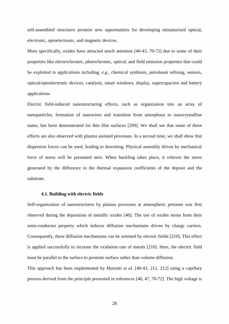
However, this afterglow-like device turns out to be of no use to organize nanostructures into
functional architectures. This problem was solved by applying the VHF field directly on a
copper electrode supporting the substrate [40-43, 211, 212]. In this configuration, it is
possible to expose the surface to a high flux of charged particles from the plasma and also to
create a very specific distribution of electric field where the field lines leave the surface of the
substrate and converge at the wire tip [40]. This phenomenon is not specific to oxides
deposition since it was also observed with carbon deposition made to grow directional
connections between silicon nanocrystals or silver nanoparticles randomly distributed on a
surface (figure 11) [40]. Modelling studies reveal that the directional growth of connections
between dots [211, 212] is controlled by surface diffusion of adatoms which is influenced by
the distribution of the local electric field around the dots. Thus, it appears that the presence of
a particle on the surface can exacerbate the local electric field and change the isotropy of
growth. It would be interesting to control independently the plasma and the electric field
distribution on the surface, the process used in references [40-43, 211, 212] coupling these
two parameters.
Self-organization of micro-filaments may be used as demonstrated by Jiang et al. [44]. As
described previously, a network of immobile streamers could be progressively created in a
DBD by tip effect on growing microstructures. These microstructures were separated one
from each other by 3 mm. They consist of particles of one hundred nanometers in diameter. It
seems likely that the charged powders formed in the gas phase are stacked on the columns
where the electric field is locally exacerbated. However, self-organization of filaments is not
so easy to control [213], and it is certainly much easier to use arrays of microplasmas [214-
216] to grow patterned objects on surfaces.
4.2. Using high temperatures and stress to control surface energies
31
For the synthesis of carbon nanotubes according to the VLS mechanism, it is possible to start
from catalyst droplets spread over the surface of the substrate used for growth. The formation
of such droplets is commonly provided by dewetting of a nanometric layer of the catalyst
deposited by various methods. This mechanism ensures naturally the formation of catalytic
nanoparticles [217, 218]. This process is studied more fundamentally in the case, for example,
of the dewetting of native silica on SOI (silicon-on-insulator) [219, 220]. The important
condition to fulfil in this case is to control the “purity” of the interface between the film and
the surface. Any contaminant affects strongly the dewetting process and the way particles get
distributed over thesurface.
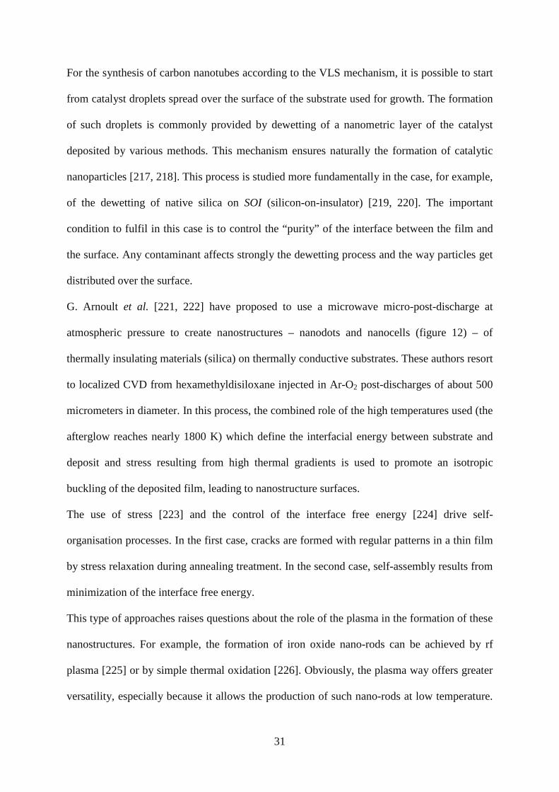
G. Arnoult et al. [221, 222] have proposed to use a microwave micro-post-discharge at
atmospheric pressure to create nanostructures – nanodots and nanocells (figure 12) – of
thermally insulating materials (silica) on thermally conductive substrates. These authors resort
to localized CVD from hexamethyldisiloxane injected in Ar-O2 post-discharges of about 500
micrometers in diameter. In this process, the combined role of the high temperatures used (the
afterglow reaches nearly 1800 K) which define the interfacial energy between substrate and
deposit and stress resulting from high thermal gradients is used to promote an isotropic
buckling of thedeposited film, leading to nanostructuresurfaces.
The use of stress [223] and the control of the interface free energy [224] drive self-
organisation processes. In the first case, cracks are formed with regular patterns in a thin film
by stress relaxation during annealing treatment. In the second case, self-assembly results from
minimization of the interface freeenergy.
This type of approaches raises questions about the role of the plasma in the formation of these
nanostructures. For example, the formation of iron oxide nano-rods can be achieved by rf
plasma [225] or by simple thermal oxidation [226]. Obviously, the plasma way offers greater
versatility, especially because it allows the production of such nano-rods at low temperature.

32
Moreover, in this example, it is also possible to grow nano-belts by adjusting the growth
temperature [227, 228]. But there are conditions of thermal oxidation, which also give the
possibility to select the morphology of nano-oxides in a wide range of possible shapes [229,
230]. Having adirectional flux of ions towards the surface in thecaseof low pressureplasmas
offers increased versatility to the process. From then on, it is nevertheless difficult to conclude
that this specificity can beextended to plasmas at atmospheric pressure.
5. Conclusion
Atmospheric plasmas have a simple implementation that makes them attractive as a source in
the production processes of nano-objects. The current methodologies are mainly based on
those established in low-pressure processes. The specificities of plasmas at high pressure, as
their small size, their self-organization or their filamentation have been little or not exploited
in thedevelopment of nanomaterials.
In this work, several important results could beemphasised:
- Self-organisation of streamers in high pressure plasmas is likely a difficult way to follow to
grow nanstructures on surface.
- Glow discharges at atmospheric pressure offer “smooth” conditions that are suitable for
controlled deposition of nanostructures over large area.
- Plasma jets are versatile tools but their performance and the reproducibility of the results is
strongly dependant on thehydrodynamic distribution of theprecursors, on theway the electric
fields are applied and on the control of the positioning of the plasma in regards to the
substrate.
- The spatial resolution of localized PECVD is not currently sufficient to build micro-electro-
mechanical-systems (MEMS) and micro-total-analytical-system (A-TAS), composed of
elements such as electrode, circuit, and channel smaller than 100 µm in diameter or width.
33
Furthermore, deposition of low melting-point materials such as polyethylene terephthalate
(PET), often used as base material for A-TAS, must bedeveloped.
- Plasma enhanced chemical vapour deposition (PECVD) process combined with nanoparticle
beams are promising hybrid processes. They offer high deposition rates, possible control of
interfaces composition and accurate localisation of thedeposition area.
- Plasmas in or on liquids show remarkable potentialities and if they are extremely simple to
use, their understanding is by far much morecomplex.
- Using templates to grow isolated objects is very well adapted to atmospheric pressure
plasmas.
- Self-organisation is possible with atmospheric pressure plasmas but only a few numbers of
routes havebeen tested and much has still do bedone to build controlled architectures.
34
Bibliography
[1] Kogelschatz U 2003 Plasma Chem. Plasma Proc. 23 1
[2] Schütze A, Jeong J Y, Babayan S E, Park J, Selwyn G S and Hicks R F 1998 IEEE Trans.
Plasma Sci. 26 1685
[3] Massines F, Rabehi A, Decomps F, Ben Gadri R, Ségur P and Mayoux C 1998 J. Appl.
Phys. 83 2950
[4] KanazawaS, KogomaM, Moriwaki T and Okazaki S 1988 J. Phys. D: Appl. Phys. 21 838
[5] Golubovskii Yu B, Maiorov V A, Behnke J and Behnke J F 2003 J. Phys. D: Appl. Phys.
36 39
[6] TachibanaK 2006 IEEJ Trans. Elec. Electron. Eng. 1 145
[7] Wang Q, Economou D J and Donnelly V M 2006 J. Appl. Phys. 100 023301
[8] Foest R, Schmidt M and Becker K 2006 Int. J. Mass Spectrom. 248 87
[9] Makasheva K, Muñoz Serrano E, Hagelaar G, Boeuf J-P and Pitchford L C 2007 Plasma
Phys. Control. Fusion 49 B233
[10] Aubert X, Bauville G, Guillon J, Lacour B, Puech V and Rousseau A 2007 Plasma
Sources Sci. Technol. 16 23
[11] Stoffels E, Flikweert A J, Stoffels W W and Kroesen G M W 2002 Plasma Sources Sci.
Technol. 11 383
[12] Laroussi M 2005 PlasmaProcess. Polym. 2 391
[13] Fridman G Friedman G Gutsol A Shekhter A B Vasilets V N and Fridman A 2008
PlasmaProcess. Polym. 5 503
[14] Boudam M K Moisan M Saoudi B Popovici C Gherardi N and Massines F 2006 J. Phys.
D: Appl. Phys. 39 3494
[15] Iza F Kim G J Lee S M Lee J K Walsh J L Zhang Y T and Kong M G 2008 Plasma
Process. Polym. 5 322

35
[16] Ichiki T, Sugiyama Y, Taura R, Koidesawa T and Horiike Y 2003 Thin Solid Films 435
62
[17] Cardoso R P, Belmonte T, Noël C, Kosior F and Henrion G 2009 J. Appl. Phys. 105
093306
[18] Brauer I, Punset C, Purwins H-G, and Boeuf J-P 1999 J. Appl. Phys. 85 7569
[19] Ráhel' J and Sherman D M 2005 J. Phys. D: Appl. Phys. 38 547
[20] Maximov A V and Schlüter H 1999 Phys. Scr. 60 556
[21] Meyyappan M, Delzeit L, Cassell A and Hash D 2003 Plasma Sources Sci. Technol. 12
205
[22] Melechko A V, Merkulov V I, McKnight T E, Guillorn M A, Klein K L, Lowndes D H
and Simpson M L 2005 J. Appl. Phys. 97 041301
[23] Ostrikov K 2005 Rev. Mod. Phys. 77 489
[24] Gordillo-Vazquez F J, Herrero V J and Tanarro I 2007 Chem.Vap. Depos. 13 267
[25] Ostrikov K 2007 IEEE Trans. Plasma Sci. 35 127
[26] Ostrikov K and Murphy A B 2007 J. Phys. D: Appl. Phys. 40 2223
[27] Ostrikov K 2009 Vacuum 83 4
[28] Kortshagen U 2009 J. Phys. D: Appl. Phys. 42 113001
[29] Meyyappan M 2009 J. Phys. D: Appl. Phys. 42 213001
[30] Mariotti D and Sankaran R M 2010 J. Phys. D: Appl. Phys. 43 323001
[31] Ostrikov K, Levchenko I, Cvelbar U, Sunkara M K and Mozetic M 2010 Nanoscale 2
2012
[32] Zheng J, Yang R, Xie L, Qu J, Liu Y and Li X 2010 Advanced Materials 22 1451
[33] Ostrikov K and Xu S “Plasma-Aided Nanofabrication: From Plasma Sources to
Nanoassembly” 2007 Wiley-VCH Verlag GmbH and Co. KGaA, Weinheim.
36
[34] Ostrikov K “Plasma Nanoscience: Basic Concepts And Applications Of Deterministic
Nanofabrication” 2008 Wiley-VCH Verlag GmbH and Co. KGaA, Weinheim.
[35] Mariotti D and Mohan Sankaran R 2011 J. Phys. D: Appl. Phys. 44 174023
[36] Ostrikov K, Long J D, Rutkevych P P and Xu S 2006 Vacuum 80 1126
[37] Ho J C, Levchenko I and Ostrikov K 2007 J. Appl. Phys. 101 094309
[38] Wang F L, Jiang J C and Meletis E I 2003 Appl. Phys. Lett. 83 2423
[39] Mitani S, Teraji T and Ito T 2006 Diamond Relat. Mater. 15 1544
[40] Mariotti D, Švrček V and Kim D-G 2007 Appl. Phys. Lett. 91 183111
[41] Mariotti D, Lindström H, Chandra BoseA and Ostrikov K 2008 Nanotechnol. 19 495302
[42] Mariotti D, ChandraBoseA and Ostrikov K 2009 IEEE Trans. Plasma Sci. 37 1027
[43] Mariotti D and Ostrikov K 2009 J. Phys. D: Appl. Phys. 42 092002
[44] Jiang N, FaQian S, Wang L and Xian Zhang H 2001 Thin Solid Films 390 119
[45] Babayan S E, Jeong J Y, Schütze A, Tu V J, Moravej M, Selwyn G S and Hicks R F
2001 Plasma Sources Sci. Technol. 10 573
[46] Shimizu Y, Sasaki T, Ito T, Terashima K and Koshizaki N 2003 J. Phys. D: Appl. Phys.
36 2940
[47] Shimizu Y, Sasaki T, Liang C, Bose A C, Ito T, Terashima K and Koshizaki N 2005
Chem. Vap. Depos. 11 244
[48] Staacks D, Gutsol A F, Friedman G and Fridman A 2008 NATO 2008 NATO Science
for Peace and Security Series A: Chemistry and Biology Plasma assisted
decontamination of biological and chemical agents, Ed. by Selçuk Gūçeri and
Alexander Fridman, Springer 79
[49] Staack D, Fridman A, Gutsol A, Gogotsi Y and Friedman G 2008 Angewandte Chemie
International Edition 47 8020
[50] Chirokov A, Gutsol A and Fridman A 2005 Pure Appl. Chem. 77 487
37
[51] Massines F, Ségur P, Gherardi N, Khamphan C and Ricard A 2003 Surf. Coat. Technol.,
174-175 8
[52] Foest R, Schmidt M and Becker K 2006 Int. J. Mass Spectrom. 248 87
[53] Laroussi M and Akan T 2007 Plasma Proc. Polym. 4 777
[54] Gomez E, Amutha Rani D, Cheeseman C R, Deegan D, Wise M and Boccaccini A R
2009 J. Hazardous Mat. 161 614
[55] Tendero C, Tixier C, Tristant P, Desmaison J and Leprince P 2006 Spectrochim. Acta
Part B: Atom. Spectrosc., 61 2
[56] Fridman A, Chirokov A and Gutsol A 2005 J. Phys. D: Appl. Phys. 38 R1
[57] Nozaki T, KimuraY and Okazaki K 2002 J. Phys. D: Appl. Phys. 35 2779
[58] Jidenko N, Jimenez C, Massines F and Borra J-P 2007 J. Phys. D: Appl. Phys. 40 4155
[59] Guo Y, Zhang J, Xu J and Yu J 2008 Appl. Surf. Sci 254 3408
[60] TanakaK, Kogoma M and OgawaY 2006 Thin Solid Films 506-507 159
[61] Lee Y-H, Kyung S-J, Kim C-W and Yeom G-Y 2006 Carbon 44 L799
[62] Lee Y-H, Kyung S-J, Jeong C-H and Yeom G-Y (2005) Jpn. J. Appl. Phys., 44 L78
[64] Park J B, Oh J S, Gil E, Kyoung S-J, Kim J-S and Yeom G-Y 2009 J. Phys. D: Appl.
Phys. 42 215201
[65] Park J B, Kyung S J and Yeom G Y 2008 J. Appl. Phys. 104 083302
[66] Kyung S-J, Lee Y-H Kim C-W, Lee J-H and Yeom G-Y 2006 Thin Solid Films 506-507
268
[66] Kyung S-J, Park J-B, Voronko M, LeeJ-H and Yeom G-Y 2007 Carbon 45 649
[67] Jiang N, Chen H-Y and Qian S-F 2005 Chin. Phys. Lett. 22 161
[68] Staack D Farouk B Gutsol A and Fridman A 2005 Plasma Sources Sci. Technol. 14 700
[69] Ito T and Terashima K 2002 Appl. Phys. Lett. 80 2648

38
[70] Shimizu Y, Chandra Bose A, Mariotti D, Sasaki T, Kirihara K, Suzuki T, Terashima K
and Koshizaki N 2006 Jpn. J. Appl. Phys. 45 8228
[71] Shimizu Y, Sasaki T, Chandra Bose A, Terashima K and Koshizaki N 2006 Surf. Coat.
Technol. 200 4251
[72] Chandra Bose A, Shimizu Y, Mariotti D, Sasaki T, Terashima K and Koshizaki N 2006
Nanotechnol. 17 5976
[73] Mariotti D, Shimizu Y, Sasaki T and Koshizaki N 2007 J. Appl. Phys. 101 013307
[74] Kikuchi T, HasegawaY and Shirai H 2004 J. Phys. D: Appl. Phys. 37 1537
[75] Narendra J J, Grotjohn T A and Asmussen J 2008 Plasma Sources Sci. Technol. 17
035027
[76] Kim J, Katsurai M, Kim D and Ohsaki H 2008 Appl. Phys. Lett. 93 191505
[77] IzaF and Hopwood J 2005 Plasma Sources Sci. Technol. 14 397
[78] Hopwood J, Iza F, Coy S and Fenner D B 2005 J. Phys. D: Appl. Phys. 38 1698
[79] Hopwood J and IzaF 2004 J. Anal. At. Spectrom. 19 1145
[80] Chiang W-H, Richmonds C and Sankaran R M 2010 Plasma Sources Sci. Technol. 19
034011
[81] Uk Bang C, Cheol Hong Y and Sup Uhm H 2007 Surf. Coat. Technol. 201 5007
[82] Hong Y C, Bang C U, Shin D H and Uhm H S 2005 Chem. Phys. Lett. 413 454
[83] Chen C-K, LeePerry W, Xu H, Jiang Y and PhillipsJ 2003 Carbon 41 2555
[84] Cheol Hong Y and Uhm H S 2005 Phys. Plasma 12 53504
[85] Hun Kim J, Cheol Hong Y and Sup Uhm H 2007 Surf. Coat. Technol. 201 5114
[86] Shin D H, Uk Bang C, Cheol Hong Y and Sup Uhm H 2006 Mat. Chem. Phys. 99 269
[87] Uhm H S, Hong Y C and Shin D H 2006 Plasma Sources Sci. Technol. 15 S26
[88] Smiljanic O, Stansfield B L, Dodelet J-P, Serventi A and Desilets S 2002 Chem. Phys.
Lett. 356 189
39
[89] Im J-H, LeeJ-H and Park D-W 2008 Surf. Coat. Technol. 202 5471
[90] Liao S-C, Lin H-F and Hong S-W 2005 “Nanostructured zinc oxide photocatalyst for
visible light and manufacturing method of thesame” US Patent 0249660
[91] Meguro T, Tsuji N, Saito S, Yamamoto Y, Mise T and Watanabe K 2008 Surf. Coat.
Technol. 202 5356
[92] Keidar M, Shashurin A, Volotskova O, Raitses Y and Beilis I I 2010 Phys. Plasmas 17
057101
[93] Keidar M, Levchenko I, Arbel T, Alexander M, Waas A M and Ostrikov K 2008 Appl.
Phys. Lett. 92 043129
[94] Keidar M, Levchenko I, Arbel T, Alexander M, Waas A M and Ostrikov K 2008 J. Appl.
Phys. 103 094318
[95] Keidar M, Raitses Y, Knapp A and Waas A M 2006 Carbon 44 1022
[96] Keidar M and Beilis I I 2009 J. Appl. Phys. 106 103304
[97] TakikawaH, Yatsuki M, SakakibaraT and Itoh S 2000 J. Phys. D: Appl. Phys. 33 826
[98] Cota-Sanchez G, Soucy G, Huczko A and Lange H 2005 Carbon 43 3153
[99] YoshidaT, Kawasaki A, NakagawaK and Akashi K 1979 J. Mater. Sci. 14 1624
[100] YoshidaT and Akashi K 1981 Trans. Japan Inst. Met. 22 371
[101] Kogelschatz U 2004 Plasma Phys. Control. Fusion 46 B63
[102] Cabral V and Silva R 2010 “Nanomaterials: Properties, Preparation and Processes”
(New York: NovaSciencePublishers)
[103] Goortani B M, MendozaN and Proulx N 2006 Int. J. Chem. React. Eng. 4 A33
[104] Vollath D 2008 J. Nanopart. Res. 10 39
[105] Jašek O, Eliáš M, Zajíčková L, Kudrle V, Bublan M, Matějková J, Rek A, Buršík J and
KadlečíkováM 2006 Mater. Sci. Eng. C 26 1189
[106] Wu L, Ma Z, HeA and Wang J 2010 J. Hazardous Mat. 173 305
40
[107] Wilson J I B, Scheerbaum N, Karim S, Polwart N, John P, Fan Y and Fitzgerald A G
(2002) Diamond Relat. Mat. 11 918
[108] Moisan M, Sauvé G, Zakrzewski J and Hubert J 1994 Plasma Sources Sci. Technol.
3 584
[109] Holländer A and Abhinandan L 2003 Surf. Coat. Technol. 174-175 1175
[110] Hafiz J, Mukherjee R, Wang X, Heberlein J V R, McMurry P H, Girshick S L 2006
Thin Solid Films 515 1147
[111] Hafiz J, Wang X, Mukherjee R, Mook W, Perrey C R, Deneen J, Heberlein J V R ,
McMurry P H , Gerberich W W, Carter C B and Girshick S L 2004 Surf. Coat.
Technol. 188–189 364
[112] Xia Y, Yang P, Sun Y, Wu Y, Mayers B, Gates B, Yin Y, Kim F and Yan H 2003 Adv.
Mater. 15 353
[113] Ito T, Izaki T and TerashimaK 2001 Thin Solid Films 386 300
[114] Ito T, Izaki T and TerashimaK 2000 Surf. Coat. Technol. 133–134 497
[115] Ito T and TerashimaK 2001 Thin Solid Films 390 234
[116] Abhinandan L and Holländer A 2004 Thin Solid Films 457 241
[117] Silmy K, Holländer A, Dillmann A and Thömel J 2005 Surf. Coat. Technol. 200 368
[118] Cardoso R P, Belmonte T, Henrion G, Gries T and Tixhon E 2010 J. Appl. Phys. 107
024909
[119] Girshick S L 2008 J. Nanopart. Res. 10 935
[120] OkumuraT, Saitoh M, Yashiro Y and KimuraT 2003 Jpn. J. Appl. Phys. 42 3995
[121] Ichiki T, TauraR, HoriikeY 2004 J. Appl. Phys. 95 35
[122] Mericam-Bourdet N, Laroussi M, Begum A and Karakas E 2009 J. Phys. D: Appl.
Phys. 42 055207
41
[123] van der Laan E P, Stoffels E and Steinbuch M 2006 Plasma Sources Sci. Technol. 15
582
[124] Kim M C, Yang S H, Boo J-H and Han J G 2003 Surf. Coat. Technol. 174-175 839
[125] Li J G, Kamiyama H, Wang X H, Moriyoshi Y and Ishigaki T 2006 J. Eur. Ceram. Soc.
26 423
[126] Li J G, Wang X H, Kamiyama H, Ishigaki T and Sekiguchi T 2006 Thin Solid Films
506–507 292
[127] Wang X H, Li J-G, Kamiyama H, Katada M, Ohashi N, Moriyoshi Y and Ishigaki T
2005 J. Am. Chem. Soc. 127 10982
[128] Zhang C, Li J, Leng Y, Uchikoshi T, Watanabe T and Ishigaki T 2010 Thin Solid Films
518 3531–4
[129] Goortani B M, Proulx P, XueS and Mendoza-Gonzalez N Y 2007 Powder Technol. 175
22
[130] Szépvölgyi J, Mohai I, Károly Z and Gál L 2008 J. Eur. Ceram. Soc. 28 895
[131] Shin J W, Miyazoe H, Leparoux M, Siegmann S, Dorier J L and Hollenstein C 2006
Plasma Sources Sci. Technol. 15 441
[132] Ishigaki T, Oh S M, Li J G and Park D W 2005 Sci. Technol. Adv. Mater. 6 111
[133] Leparoux M, Schreuders C, Shin J W and Siegman S 2005 Adv. Eng. Mater. 7 349
[134] Leconte Y, Leparoux M, Portier X and Herlin-Boime N 2008 Plasma Chem. Plasma
Process. 28 233
[135] Leparoux M, Kihn Y, Paris S and Schreuders C 2008 Int. J. Refract. Met. Hard Mater.
26 277
[136] Bai H, Chen C, Lin C, Den W and Chang C 2004 Ind. Eng. Chem. Res. 43 7200
[137] BorraJ P, Jidenko N and Bourgeois E 2009 Eur. Phys. J. Appl. Phys. 47 22804
[138] Lei H, Tang Y, Li J, Luo J and Li X 2006 Appl. Phys. Lett. 88 083111
42
[139] Chiang W-H and Mohan Sankaran R 2007 Appl. Phys. Lett. 91 121503
[140] Chiang W-H and Mohan Sankaran R 2008 J. Phys. Chem. C 112 17920
[141] Chiang W-H and Mohan Sankaran R 2008 Adv. Mater. 20 4857
[142] Liu M, Lu G and Chen J 2008 Nanotechnol. 19 265705
[143] Kim J H, Hong Y C and Uhm H S 2007 Jap. J. Appl. Phys. 46 4351
[144] Demoisson F, Raes M, Terryn H, Guillot J, Migeon H-N and Reniers F 2008 Surf.
Interface Anal. 40 566
[145] Shim J, Joung K Y, Ahn J H and LeeW M 2007 J. Electrochem. Soc. 154 B165
[146] Rahman M, Amsarani R, Mooney D A, MacElroy J M D and Dowling D P 2009 J.
Nanosci. Nanotechnol. 9 3506
[147] Gok A and Oksuz L 2007 J. Macromol. Sci. A: Pure Appl. Chem. 44 1095
[148] Zou Q and Wang M Z 2009 Micro Nano Lett. 4 63
[149] Bian X, Chen Q, Zhang Y, Sang L and Tang W 2008 Surf. Coat. Technol. 202 5383
[150] Terajima T, Chaudhary K A, Inomata K and Koinuma H 2003 J. Nanosci. Nanotechnol.
13 231
[151] Dato A, Radmilovic V, Zonghoon Lee, Phillips J and Frenklach M 2008 Nano Lett. 8
2012
[152] Zou Q, Wang M Z, Li Y G and Zou L H 2009 J. Low. Temp. Phys. 157 557
[153] Moreno-Couranjou M, Monthioux M, Gonzalez-Aguilar J and Fulcheri L 2009 Carbon
47 2310
[154] Kashu S, FuchitaE, ManabeT and Hayashi C 1984 Jpn. J. Appl. Phys. 23 L910
[155] Oda M, Katsu I, Tsuneizumi M, Fuchita E, Kashu S and Hayashi C 1993 Mater. Res.
Soc. Symp. Proc. 286 121.
[156] Schroth A, Maeda R, Akedo J and Ichiki M 1998 Jpn. J. Appl. Phys. 37 5342
[157] Akedo J and Lebedev M 1999 Jpn. J. Appl. Phys. 38 5397
43
[158] Akedo J, Ichiki M, Kikuchi K and MaedaR 1998 Sens. Actuators A 69 106
[159] Rao N P, Lee H J, Kelkar M, Hansen D J, Heberlein J V R, McMurry P H and Girshick
S L 1997 Nanostruct. Mater. 9 129
[160] Rao N P, Tymiak N, Blum J, Neuman A, Lee H J, Girshick S L, McMurry P H and
Heberlein J 1998 J. Aerosol. Sci. 29 707
[161] Rao N P, Girshick S L, McMurry P H and Heberlein J V R 1999 “Production of
nanostructured materials by hypersonic plasmaparticledeposition” US Patent 5874134
[162] Rao N P, Heberlein J V R, Gerberich W W, Girshick S L and McMurry P H 2005
“Apparatus and method for synthesizing films and coatings by focused particle beam
deposition” US patent 6924004
[163] Blum J, Tymiak N, Neuman A, Wong Z, Rao N P, Girshick S L, Gerberich W W,
McMurry P H and Heberlein J V R 1999 J. Nanopart. Res. 1 31
[164] Hafiz J, Mukherjee R, Wang X, McMurry P H, Heberlein J V R and Girshick S L 2006
J. Thermal Spray Technol. 15 822
[165] Roca i Cabarrocas P, Fontcuberta i Morral A, Lebib S and Poissant Y 2002 Pure Appl.
Chem. 74 359
[166] Chaabane N, Suendo V, Vach H and Roca i Cabarrocas P 2006 Appl. Phys. Lett. 88
203111
[167] Kakiuchi H, Nakahama Y, Ohmi H, Yasutake K, Yoshii K and Mori Y 2005 Thin Solid
Films 479 17
[168] Mori Y, Yoshii K, Kakiuchi H and YasutakeK 2000 Rev. Sci. Instrum. 71 3173
[169] Mori Y, Yoshii K, Yasutake K, Kakiuchi H, Ohmi H and Wada K 2003 Thin Solid
Films 444 138
[170] Mori Y, Kakiuchi H, Yoshii K, Yasutake K and Ohmi H 2003 J. Phys. D: Appl. Phys.
36 3057
44
[171] Barry C R, Lwin N Z, Zheng W and Jacobs H O 2003 Appl. Phys. Lett. 83 5527
[172] ColeJ J, Lin E-C, Barry C R and Jacobs H O 2009 Appl. Phys. Lett. 95 113101
[173] Vons V, Creyghton Y and Schmidt-Ott A 2006 J. Nanopart. Res. 8 721
[174] Marino E, Huijser T, Creyghton Y, van der Heijden A 2007 Surf. Coat. Technol. 201
9205
[175] HeW, Guo Z, Pu Y, Yan L and Si W 2004 Appl. Phys. Lett. 85 896
[176] SzabováR, Černáková L, WolfováM andČernák M 2009 Acta Chimica Slovaca 2 70
[177] Nessim C, Boulos M and Kogelschatz U 2009 Eur. Phys. J. Appl. Phys. 47 22819
[178] Mori T, TanakaK, InomataT, TakedaA and KogomaM 1998 Thin Solid Films 316 89
[179] NakajimaT, TanakaK, InomataT and KogomaM 2001 Thin Solid Films 386 208
[180] OgawaS, Takeda A, Oguchi M, TanakaK, InomataT and Kogoma M 2001 Thin Solid
Films 386 213
[181] Jung S H, Park SM, Park S H and Kim S D 2004 Ind. End. Chem. Res. 43 5483
[182] Li M-X, Hu Z, Wang X-Z, Wu Q and Chen Y 2003 Thin Solid Films 435 116
[183] Li M-X, Hu Z, Wang X-Z, Wu Q, Chen Y and Tian Y-L 2004 Diamond Relat. Mater.
13 111
[184] Jeong S-H, Hwang H-Y, Hwang S-K and LeeK-H 2004 Carbon 42 2073
[185] Wang C X, Ren Y and Qiu Y P 2007 Surf. Coat. Technol. 202 77
[186] Wang C X, Liu Y, Xu H L, Ren Y and Qiu Y P 2008 Appl. Surf. Sci. 254 2499
[187] Ghadimi A, Cademartiri L, Kamp U and Ozin G A 2007 Nano Letters 7 3864
[188] Cademartiri L, von Freymann G, Arsenault A C, Bertolotti J, Wiersma D S, Kitaev V
and Ozin G A 2005 Small 1 1184
[189] Teo K B K, Chhowalla M, Amaratunga G A J, Milne W I, Hasko D G, Pirio G,
Legagneux P, Wyczisk F and Pribat D 2001 Appl. Phys. Lett. 79 1534
45
[190] Fan S, Chapline M G, Franklin N R, Tombler T W, Cassell A M and Dai H 1999
Science 283 512
[191] Wei B Q, Vajtai R, Jung Y, Ward J, Zhang R, Ramanath G and Ajayan P M 2002
Nature 416 495
[192] Merkulov V I, Lowndes D H, Wei Y Y, Eres G and Voelkl E 2000 Appl. Phys. Lett. 76
3555
[193] Sohn J I, Lee S, Song Y-H, Choi S-Y, Cho K-I and Nam K-S 2001 Appl. Phys. Lett. 78
901
[194] Barankin M Creyghton Y and Schmidt-Ott A 2006 J. Nanoparticle Res. 8 511
[195] Hinkov I, Farhat S and Scott C D 2005 Carbon 43 2453
[196] Jašek O, Eliáš M, Zajíčková L, Kučerová Z, Matějková J, Rek A and Buršík J 2007 J.
Phys. Chem. Solids 68 738
[197] Kyung S-J, LeeY-H, Kim C-W, LeeJ-H and Yeom G-Y 2006 Carbon 44 1530
[198] Kyung S-J, Voronko M, Lee Y-H, Kim C-W, Lee J-H and Yeom G-Y 2007 Surf. Coat.
Technol. 201 5378
[199] Lee Y-H, Jang H-S, Eom G-Y, Lee B-J, Burk D, Overzet L and Lee G S 2008 Mater.
Lett. 62 3849
[200] Nozaki T and Okazaki K 2008 Plasma Proc. Polym. 5 300
[201] Yoshiki H, Okada T, Hirai K and HatakeyamaR 2006 Jap. J. Appl. Phys. 45 9276
[202] Mishra L N, Shibata K, Ito H, Yugami N and Nishida Y 2004 IEEE Trans. Plasma Sci.
32 1727
[203] Matsushita A, Nagai M, Yamakawa K, Hiramatsu M, Sakai A, Hori M, Goto T and
ZaimaS 2004 Jap. J. Appl. Phys. 43 424
[204] Choi B H, Kim W J, Kim Y B, Lee J H, Park J W, Kim W S and Shin D C 2008 J.
Nanosci. Nanotechnol. 8 4999
46
[205] Zhang Y-P, Liu C-J and Zhang M-H 2000 Chem. Lett. 10 1204
[206] Chandrashekar A, Lee J-S, Lee G S, Goeckner M J and Overzet L J 2006 J. Vac. Sci.
Technol. A 24 1812
[207] Nozaki T, Karatsu T, Ohnishi K and Okazaki K 2010 Carbon 48 232
[208] Shirai H, Kobayashi T and HasegawaY 2005 Appl. Phys. Lett. 87 143112
[209] Kumar P 2010 Nanoscale Res. Lett. 5 1367
[210] Atkinson A 1985 Rev. Modern Phys. 57 437
[211] Levchenko I, Ostrikov K, Mariotti D and Švrček V 2009 Carbon 47 2379
[212] Levchenko I, Ostrikov K and Mariotti D 2009 Carbon 47 313
[213] Li-Fang D, Ya-Feng H, Zeng-Qian Y and Zhi-Fang C 2003 Chin. Phys. Lett. 20 1524
[214] Eden J G, Park S-J, Ostrom N P and Chen K-F 2005 J. Phys. D: Appl. Phys. 38 1644
[215] Becker K H, Schoenbach K H and Eden J G 2006 J. Phys. D: Appl. Phys. 39 R55
[216] Chai J, Li B, Kwok D Y 2005 Appl. Phys. Lett. 86 034107
[217] Akinwande D, Patil N, Lin A, Nishi Y and Philip Wong H-S 2009 J. Phys. Chem. C
113 8002
[218] Nessim G D, Hart A J, Kim J S, Acquaviva D, Oh J, Morgan C D, Seita M, Leib J S,
and Thompson C V 2008 Nano Lett. 8 3587
[219] Danielson D T, Sparacin D K, Michel J and Kimerling L C 2006 J. Appl. Phys. 100
083507
[220] Pierre-Louis O, ChameA and Saito Y 2007 Phys. Rev. Lett. 99 136101
[221] Arnoult G, Cardoso R P, BelmonteT and Henrion G 2008 Appl. Phys. Lett. 93 191507
[222] Arnoult G, BelmonteT and Henrion G 2010 Appl. Phys. Lett. 96 101505
[223] Bowden N, Terfort A and Carbeck Whitesides G M 1997 Science 276 233
[224] Erdem AlacaB, Sehitoglu H and Saif T 2004 Appl. Phys. Lett. 84 4669
[225] MozetičM, Cvelbar U, SunkaraM K and Vaddiraju S 2005 Adv. Mater. 17 2138

47
[226] Fu Y Chen J and Zhang H 2001 Chem. Phys. Lett. 350 491
[227] Chen Z, Cvelbar U, MozetičM, HeJ and SunkaraM K 2008 Chem. Matter. 20 3224
[228] Cvelbar U, Chen Z, SunkaraM K and MozetičM 2008 Small 4 1610
[229] Dai Z R, Pan Z W and Wang Z L 2003 Adv. Funct. Mater 13 9
[230] Ren S, Bai Y F, Chen J, Deng S Z, Xu N S, Wu Q B and Yang S 2007 Mat. Lett. 61 666
48
Captions
Figure 1: Examples of DBD reactors for large area. a) dissymmetric arrangement (after Jiang
et al. [44]). b) Pin-to-plate dielectric barrier discharge composed of a multi-pin power
electrode (after Kyung et al. [63]). c) Similar source with an aluminium power electrode
coated by alumina (after Park et al. [65]). d) Dielectric barrier with capillary holes proposed
by Kyung et al. [66] to get a more uniform reactive gas distribution. Similar process with a
metallic grid electrode made placed between the dielectric barrier and the substrate (after
Jiang et al. [67]).
Figure 2: Examples of microplasma jets. a) Capillary with a pinched nozzlewound around by
a 5-turn coil connected to a 450 MHz UHF generator. A tungsten wire connected to a 15 kV
dc power supply is used for plasma ignition (After Shimizu et al. [46]). b) Capillary with a
pinched nozzle wound around by a 20-turn coil (After Chandra Bose et al. [72] and Shimizu
et al. [70]). c) Capillary with wire. The UHF signal is applied on a patch antenna (after
Mariotti et al. [40]). d) Additional annular nozzle used for etching (after Ichiki et al. [16]). e)
Capillary with wireused as an antenna (after Kikuchi et al. [74]).
Figure 3: Microplasmas used as component of an electric circuit where charge conduction
occurs through a liquid [80]. The microplasma is formed at the surface of an electrolyte and
operated as the cathode, with an immersed solid metal electrode as the anode, creating a
hybrid plasma–liquid electrochemical cell. At the anode, oxidation reactions leads to
dissolution of thesolid metal into metal cations which were then reduced at thecathodeby the
microplasma to nucleate metal nanoparticles.
Figure 4: Examples of plasma torches at or not too far from thermal equilibrium. a) Plasma
torches excited by microwave power supplies [81-88]. b) Plasma torches excited by dc [89-
91]. c) possible arrangements to introduce precursors in the dc torch. d) rf induction plasma
torch.
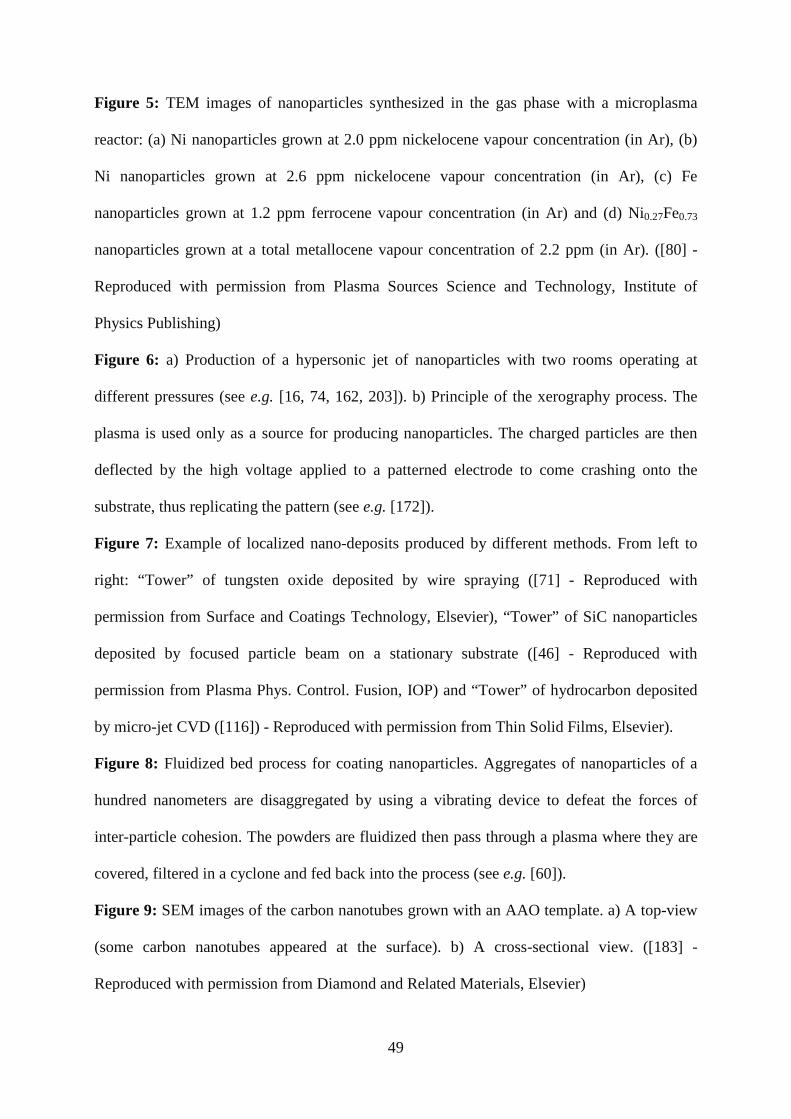
49
Figure 5: TEM images of nanoparticles synthesized in the gas phase with a microplasma
reactor: (a) Ni nanoparticles grown at 2.0 ppm nickelocene vapour concentration (in Ar), (b)
Ni nanoparticles grown at 2.6 ppm nickelocene vapour concentration (in Ar), (c) Fe
nanoparticles grown at 1.2 ppm ferrocene vapour concentration (in Ar) and (d) Ni0.27Fe0.73
nanoparticles grown at a total metallocene vapour concentration of 2.2 ppm (in Ar). ([80] -
Reproduced with permission from Plasma Sources Science and Technology, Institute of
Physics Publishing)
Figure 6: a) Production of a hypersonic jet of nanoparticles with two rooms operating at
different pressures (see e.g. [16, 74, 162, 203]). b) Principle of the xerography process. The
plasma is used only as a source for producing nanoparticles. The charged particles are then
deflected by the high voltage applied to a patterned electrode to come crashing onto the
substrate, thus replicating thepattern (see e.g. [172]).
Figure 7: Example of localized nano-deposits produced by different methods. From left to
right: “Tower” of tungsten oxide deposited by wire spraying ([71] - Reproduced with
permission from Surface and Coatings Technology, Elsevier), “Tower” of SiC nanoparticles
deposited by focused particle beam on a stationary substrate ([46] - Reproduced with
permission from Plasma Phys. Control. Fusion, IOP) and “Tower” of hydrocarbon deposited
by micro-jet CVD ([116]) - Reproduced with permission from Thin Solid Films, Elsevier).
Figure 8: Fluidized bed process for coating nanoparticles. Aggregates of nanoparticles of a
hundred nanometers are disaggregated by using a vibrating device to defeat the forces of
inter-particle cohesion. The powders are fluidized then pass through a plasma where they are
covered, filtered in a cycloneand fed back into the process (see e.g. [60]).
Figure 9: SEM images of the carbon nanotubes grown with an AAO template. a) A top-view
(some carbon nanotubes appeared at the surface). b) A cross-sectional view. ([183] -
Reproduced with permission from Diamond and Related Materials, Elsevier)

50
Figure 10: Example of a method based on the use of templates (see e.g. [146]). The pores of
an anodized alumina plate (Anodic Aluminum Oxide for AAO) are used to grow carbon
nanowires. First, the pores of the AAO template are widened by chemical etching in aqueous
phosphoric acid. Second, a small amount of Fe-Co catalytic particles are electrodeposited into
the template pores. Third, CH4 and H2 (1:10) are fed into the reactor at a total feed rate of 22
ml min−1. The corona discharge is pulsed for 10 min with a high voltage generator operating
at 2800 V and 50 kpps with the power of 10 W. Fourth, alumina is dissolved in a solution of
sodium hydroxide to get thecarbon nanowires standing on thesurface.
Figure 11: SEM images of self-organized nanostructures grown with a microplasma system
based on a patch antenna and using a microdiameter capillary. a) self-aligned Mo-oxide
structures b) Carbon-based connections between Ag particles ([40] - Reproduced with
permission from Applied Physics Letters, American Instituteof Physics)
Figure 12: SEM images of silica cells and dots deposited with a micro-afterglow at
atmospheric pressure by chemical vapour deposition using HMDSO. The stress level controls
theself-organisation of thesestructures [221, 222].
Table 1: Some characteristics of microplasma jets used for localized PECVD at atmospheric
pressure.

51
Gases~
Heater
Heater
Substrate
= Al2O3 dielectric
~
Grid
d)
e)
Gases3 mm
7.5 mm
10 mm1 mm
20-100 kHz
100 kHz
~b)
Gases> 1 mm
50 mm30 kHz
~c)
Gases
50 mm30 kHz
1 mm
Subs
trat
e
~a)
Gases
50 mm3 kHz
2 mm
Figure 1
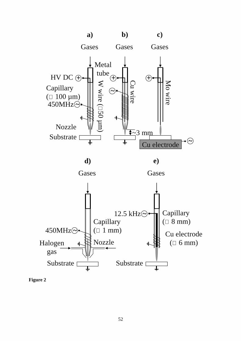
52
Gases
a)
Capillary(∅ 100 µm)
HV DC
450MHz ~
Nozzle
Ww
ire(∅
50µ
m)
Metaltube
Substrate
Gases
b)
Cu
wire
Gases
c)
Mo
wire
Cu electrode
~
~
+ ++
~3 mm
Gases
d)
Capillary(∅ 1 mm)450MHz ~
Nozzle
Substrate
Halogengas
Gases
e)
Capillary(∅ 8 mm)
Cu electrode(∅ 6 mm)
Substrate
12.5 kHz ~
Figure 2

53
ArRballast
M�
Mn++
ne
−
(Mn+)
(Mn+)
+n
e−�
[M]
[M]i +
[M]�
[M]i+
1 electrolyte
microplasmaDC power
supplye− e−
Figure 3
54
Swirlinggases
b) +
Water in
Water out
Quenching tube
Precursor
Collector
Precursor
Swirlinggases
Precursor
Swirlinggases
+
Microwavepower supply
Stub tuner
Circulator
Fused silica tubeSwirlinggases
a)
Taperedwaveguide
Collector
Rf coils
c) d) Precursor
Gascurtain Central gas
Figure 4

55
Figure 5
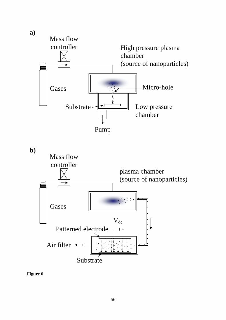
56
Gases
a)Mass flowcontroller High pressure plasma
chamber(source of nanoparticles)
Low pressurechamber
Pump
Micro-hole
Substrate
Gases
b) Mass flowcontroller
plasma chamber(source of nanoparticles)
Patterned electrodeVdc
Substrate
Air filter
Figure 6
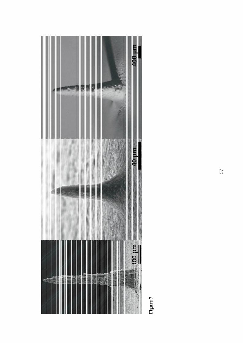
57
Fig
ure
7
400
µm40
µm
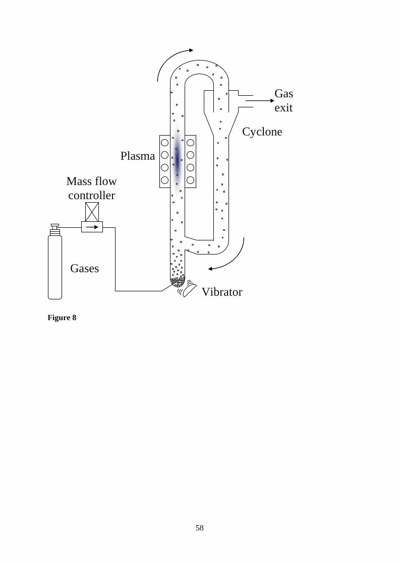
58
Gases
Mass flowcontroller
Plasma
Gasexit
Cyclone
Vibrator
Figure 8
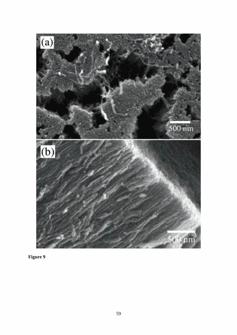
59
Figure 9
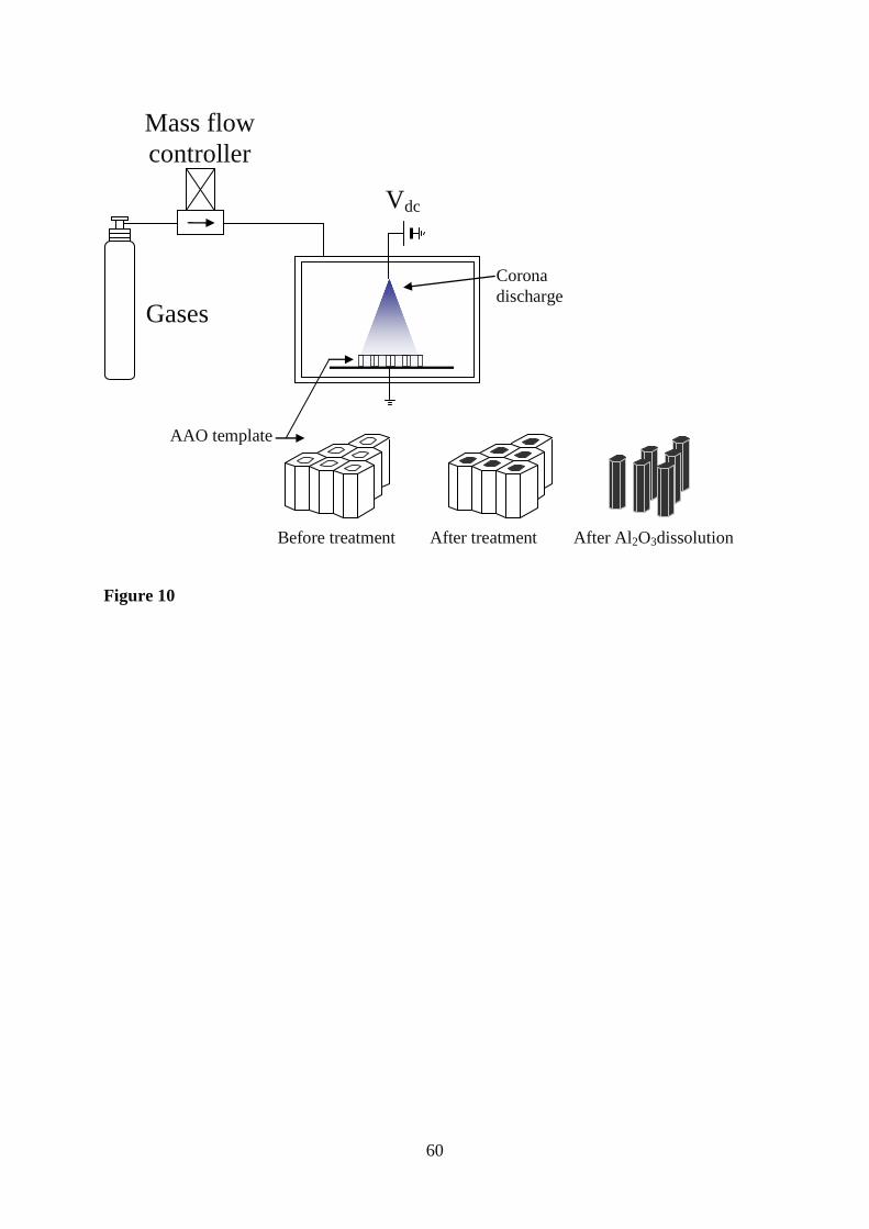
60
Gases
Mass flowcontroller
Vdc
AAO template
Coronadischarge
Before treatment After treatment After Al2O3dissolution
Figure 10
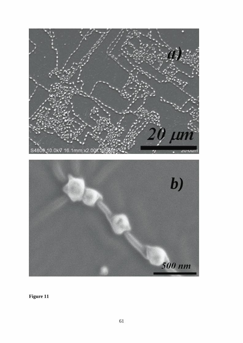
61
Figure 11
b)
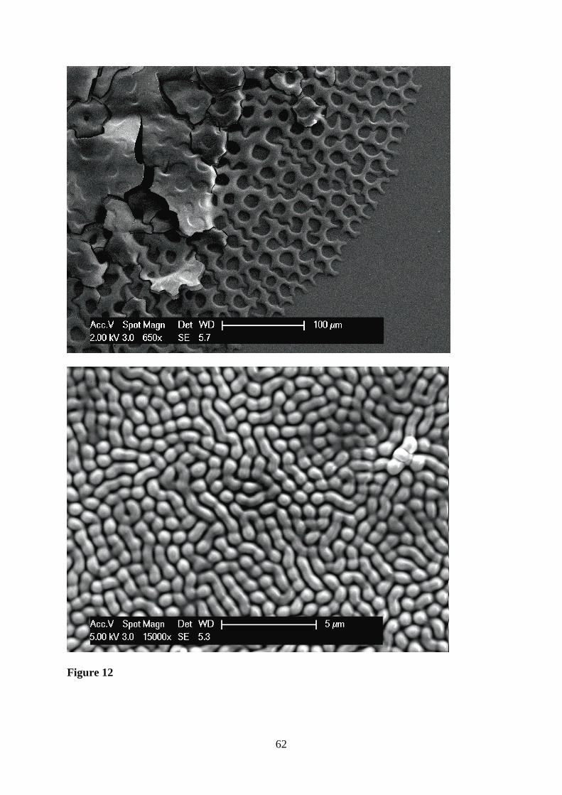
62
Figure 12
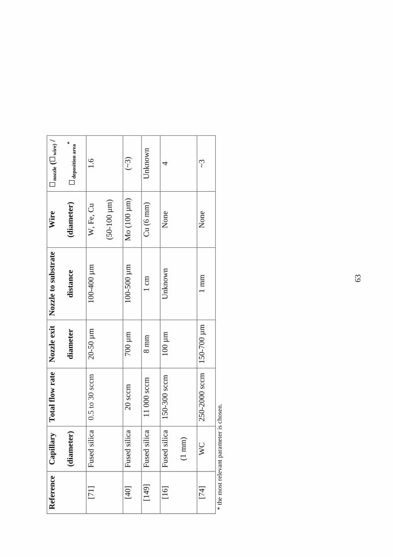
63
Ref
eren
ceC
apill
ary
(dia
met
er)
Tot
alfl
owra
teN
ozzl
eex
it
diam
eter
Noz
zle
tosu
bstr
ate
dist
ance
Wir
e
(dia
met
er)
∅no
zzle
(∅w
ire)
/
∅de
posi
tion
area
*
[71]
Fuse
dsi
lica
0.5
to30
sccm
20-5
0µ
m10
0-40
0µ
mW
,Fe,
Cu
(50-
100
µm
)
1.6
[40]
Fuse
dsi
lica
20sc
cm70
0µ
m10
0-50
0µ
mM
o(1
00µ
m)
(~3)
[149
]Fu
sed
sili
ca11
000
sccm
8m
m1
cmC
u(6
mm
)U
nkno
wn
[16]
Fuse
dsi
lica
(1m
m)
150-
300
sccm
100
µm
Unk
now
nN
one
4
[74]
WC
250-
2000
sccm
150-
700
µm
1m
mN
one
~3
*th
em
ostr
elev
antp
aram
eter
isch
osen
.


![3D numerical simulation of the electric arc motion between ... · Thermal plasmas 2 Thermal plasmas characteristics: ~104𝐾 Local Thermodynamic Equilibrium (LTE) [1] M. I. Boulos,](https://img.pdfslide.net/doc/110x75/5fd9098e282efc5f852ce2e6/3d-numerical-simulation-of-the-electric-arc-motion-between-thermal-plasmas-2.jpg)