Embed Size (px)
Citation preview
Nanotribology and nanomechanics innano/biotechnology
BY BHARAT BHUSHAN*
Nanotribology Laboratory for Information Storage and MEMS/NEMS, TheOhio State University, 201 West 19th Avenue, Columbus, OH 43210-1142, USA
Owing to larger surface area in micro/nanoelectromechanical systems (MEMS/NEMS),surface forces such as adhesion, friction, and meniscus and viscous drag forces becomelarge when compared with inertial and electromagnetic forces. There is a need to developlubricants and identify lubrication methods that are suitable for MEMS/NEMS. ForBioMEMS/BioNEMS, adhesion between biological molecular layers and the substrate,and friction and wear of biological layers may be important, and methods to enhanceadhesion between biomolecules and the device surface need to be developed. There is aneed for development of a fundamental understanding of adhesion, friction/stiction, wear,the role of surface contamination and environment, and lubrication. MEMS/NEMSmaterials need to exhibit good mechanical and tribological properties on themicro/nanoscale. Most mechanical properties are known to be scale dependent.Therefore, the properties of nanoscale structures need to be measured. Component-level studies are required to provide a better understanding of the tribologicalphenomena occurring in MEMS/NEMS. The emergence of micro/nanotribology andatomic force microscopy-based techniques has provided researchers with a viableapproach to address these problems. This paper presents an overview of micro/nanoscaleadhesion, friction, and wear studies of materials and lubrication studies forMEMS/NEMS and BioMEMS/BioNEMS. It also presents a review of scale-dependentmechanical properties, and stress and deformation analysis of nanostructures.
Keywords: nanotribology; nanomechanics; microelectromechanical systems;nanoelectromechanical systems; bioMEMS; bioNEMS
Onnan
*bh
1. Introduction
Microelectromechanical systems (MEMS) refer to microscopic devices that have acharacteristic length of less than 1 mm but more than 100 nm and combineelectrical and mechanical components. Nanoelectromechanical systems (NEMS)refer to nanoscopic devices that have a characteristic length of less than 100 nmand combine electrical and mechanical components. In mesoscale devices, if thefunctional components are on micro- or nanoscale, they may be referred to asMEMS or NEMS, respectively. These are referred to as an intelligent miniaturized
Phil. Trans. R. Soc. A (2008) 366, 1499–1537
doi:10.1098/rsta.2007.2170
Published online 11 January 2008
e contribution of 7 to a Theme Issue ‘Nanotribology, nanomechanics and applications tootechnology II’.
1499 This journal is q 2008 The Royal Society
Table 1. Dimensions and masses in perspective.
(a) dimensions in perspectivehuman hair w75 000 nm in diameterbiological cells in the range of thousands of nm in diameterDNA molecules w2.5 nm wideindividual atoms typically a fraction of a nm in diameter
NEMS characteristic length !100 nmMEMS characteristic length !1 mm and O100 nm
molecular gear w10 nmvertical SWCNT transistor w15 nmquantum-dots transistor 300 nmdigital micromirror 12 000 nm
(b) weight in perspectiveNEMS built with cross sections
of approximately 10 nmas low as 10K20 N
micromachined silicon structure as low as 1 nNwater droplet w10 mNeyelash w100 nN
B. Bhushan1500
system comprising sensing, processing and/or actuating functions, and combineelectrical and mechanical components. The acronym MEMS originated in theUSA. The term commonly used in Europe is microsystem technology (MST) andin Japan is micromachines. Another term generally used is micro/nanodevices.MEMS/NEMS terms are also now used in a broad sense and include electrical,mechanical, fluidic, optical and/or biological functions. MEMS/NEMS for opticalapplications are referred to as micro/nanooptoelectromechanical systems(MOEMS/NOEMS). MEMS/NEMS for electronic applications are referred toas radiofrequency MEMS/NEMS or RF-MEMS/RF-NEMS. MEMS/NEMS forbiological applications are referred to as BioMEMS/BioNEMS. These devices areproduced by either top–down (lithographic, non-lithographic or micromachining)or bottom–up (nanochemistry) processes.
To put the dimensions of MEMS and NEMS in perspective, see table 1.Individual atoms are typically a fraction of one nanometre in diameter, DNAmolecules are approximately 2.5 nm wide, biological cells are in the range ofthousands of nanometres in diameter and human hair is approximately 75 mm indiameter. Three NEMS reported in the table range in size from 10 to 300 nm andone MEMS reported is 12 000 nm. The weight of a micromachined siliconstructure can be as low as 1 nN, and NEMS can be built with weight as low as10K20 N with cross sections of approximately 10 nm. In comparison, the weightof a drop of water is approximately 10 mN and that of an eyelash isapproximately 100 nN.
A broad class of MEMS/NEMS are used in electromechanical, electronics,information/communication, chemical and biological applications (Bhushan2007a).MEMS for mechanical applications include acceleration, pressure, flow and gassensors, linear and rotary actuators, and other microstructures or microcomponentssuch as electric motors, gear chains, gas turbine engines, fluid pumps, fluid valves,switches, grippers and tweezers. MEMS for chemical applications include chemicalsensors and various analytical instruments. MOEMS are the devices that include
Phil. Trans. R. Soc. A (2008)
1501Nanotribology and nanomechanics
optical components, such as micromirror arrays for displays, infrared image sensors,spectrometers, bar code readers and optical switches. RF-MEMS include inductors,capacitors, antennas and RF switches. High aspect ratio MEMS (HARMEMS)have also been introduced. Examples of NEMS include microcantilevers withintegrated sharp nanotips for scanning tunnelling microscopy (STM) and atomicforce microscopy (AFM), quantum corral are formed using STM by placing atomsone by one, AFM cantilever array (Millipede) for data storage, STM and AFM tipsfor nanolithography, dip pen nanolithography for printing molecules, nanowires,carbon nanotubes, quantum wires (QWRs), quantum boxes (QBs), quantumtransistors, nanotube-based sensors, biological (DNA) motors, molecular gears byattaching benzene molecules to the outer walls of carbon nanotubes, devicesincorporating nanometre-thick films (e.g. in giant magnetoresistive or GMR read/writemagnetic heads andmagnetic media formagnetic rigid disk andmagnetic tapedrives), nanopatterned magnetic rigid disks and nanoparticles (e.g. nanoparticles inmagnetic tape substrates and nanomagnetic particles in magnetic tape coatings).
BioMEMS/BioNEMS are increasingly used in commercial and defenceapplications (Bhushan 2007a). They are used for chemical and biochemicalanalyses (biosensors) in medical diagnostics (e.g. DNA, RNA, proteins, cells,blood pressure and assays and toxin identification), tissue engineering andimplantable pharmaceutical drug delivery. Biosensors, also referred to as biochips,deal with liquids and gases. There are two types of biosensors. A large variety ofbiosensors are based on micro/nanofluidics. Micro/nanofluidic devices offer theability to work with smaller reagent volumes and shorter reaction times, andperform analyses of multiple types at once. The second type of biosensors includesmicro/nanoarrays that perform one type of analysis thousands of times.
(a ) Examples of devices with tribological issues in MEMS/NEMS andBioMEMS/BioNEMS
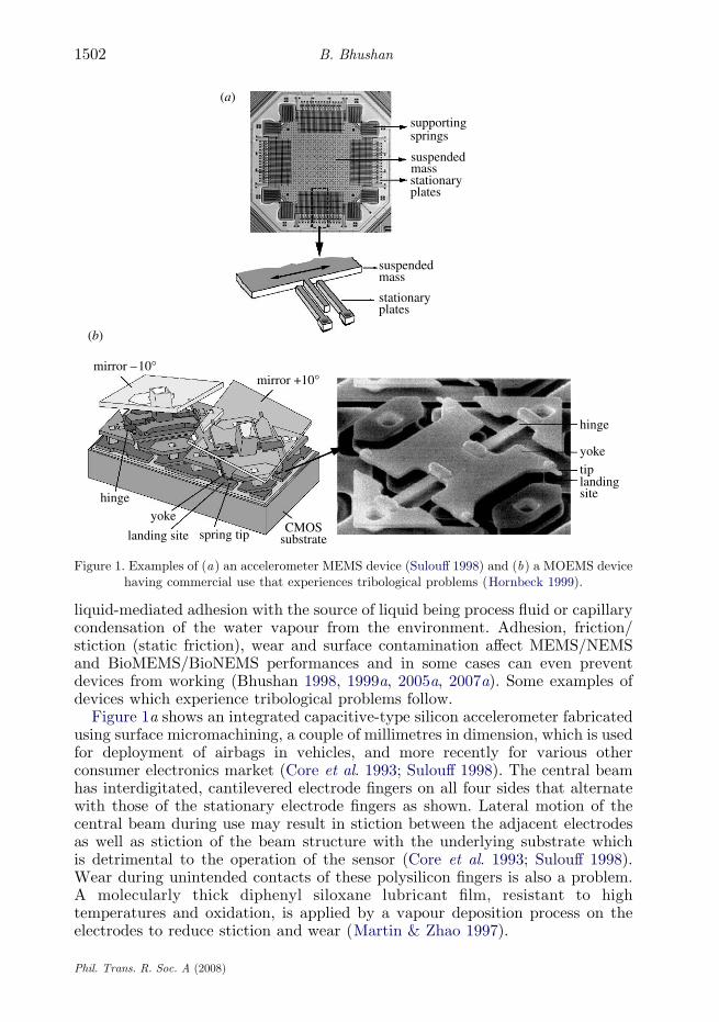
Tribological issues are important in MEMS/NEMS and BioMEMS/BioNEMSrequiring intended and/or unintended relative motion. In these devices, variousforces associated with the device scale down with the size. When the length of themachine decreases from 1 mm to 1 mm, the surface area decreases by a factor of amillion and the volume decreases by a factor of a billion. As a result, surfaceforces such as adhesion, friction, meniscus forces, viscous drag forces and surfacetension that are proportional to surface area become a thousand times largerthan the forces proportional to the volume, such as inertial and electromagneticforces. In addition to the consequences of the large surface-to-volume ratios, thesmall tolerances that these devices are designed for make physical contacts morelikely, thereby making them particularly vulnerable to adhesion betweenadjacent components. Slight particulate or chemical contamination present atthe interface can be detrimental. Furthermore, the small start-up forces and thetorques available to overcome retarding forces are small, and the increase inresistive forces such as adhesion and friction becomes a serious tribologicalconcern, which limits the durability and reliability of MEMS/NEMS (Bhushan1998). A large lateral force required to initiate relative motion between twosurfaces, large static friction, is referred to as ‘stiction’, which has been studiedextensively in tribology of magnetic storage systems (Bhushan 1996, 1999a,b,2001, 2002, 2003, 2005a,b, 2007b). The source of stiction is generally
Phil. Trans. R. Soc. A (2008)
supportingsprings
suspendedmass
suspendedmass
stationaryplates
stationaryplates
(a)
(b)
mirror +10°mirror –10°
hinge
hinge
yoke
yoke
landing site
landingsite
spring tip CMOSsubstrate
tip
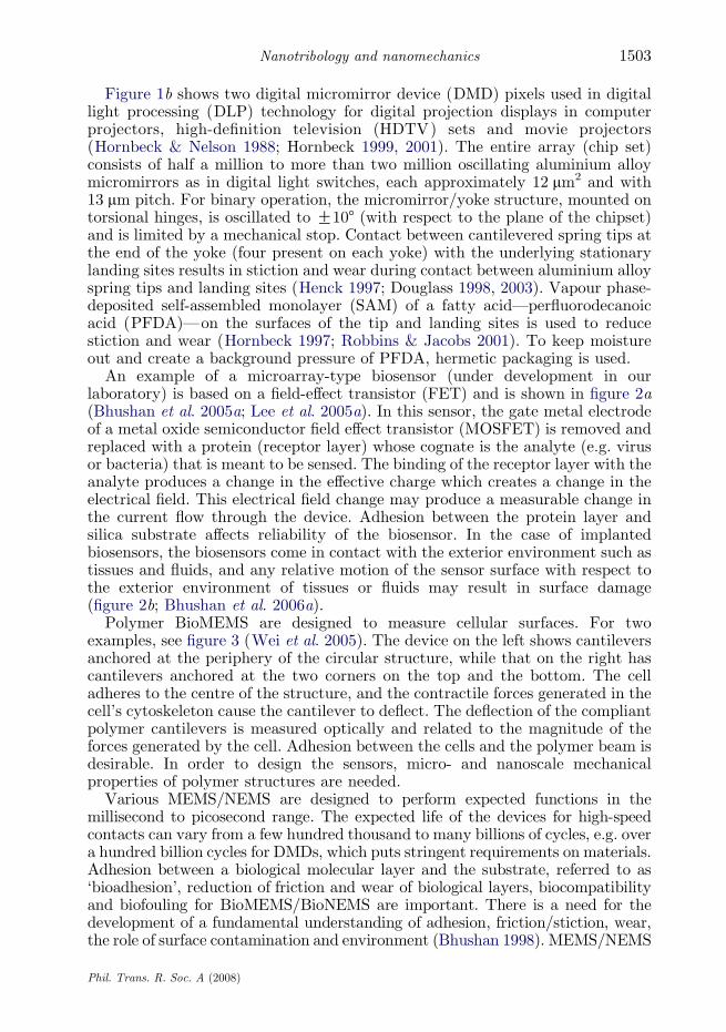
Figure 1. Examples of (a) an accelerometer MEMS device (Sulouff 1998) and (b) a MOEMS devicehaving commercial use that experiences tribological problems (Hornbeck 1999).
B. Bhushan1502
liquid-mediated adhesion with the source of liquid being process fluid or capillarycondensation of the water vapour from the environment. Adhesion, friction/stiction (static friction), wear and surface contamination affect MEMS/NEMSand BioMEMS/BioNEMS performances and in some cases can even preventdevices from working (Bhushan 1998, 1999a, 2005a, 2007a). Some examples ofdevices which experience tribological problems follow.
Figure 1a shows an integrated capacitive-type silicon accelerometer fabricatedusing surface micromachining, a couple of millimetres in dimension, which is usedfor deployment of airbags in vehicles, and more recently for various otherconsumer electronics market (Core et al. 1993; Sulouff 1998). The central beamhas interdigitated, cantilevered electrode fingers on all four sides that alternatewith those of the stationary electrode fingers as shown. Lateral motion of thecentral beam during use may result in stiction between the adjacent electrodesas well as stiction of the beam structure with the underlying substrate whichis detrimental to the operation of the sensor (Core et al. 1993; Sulouff 1998).Wear during unintended contacts of these polysilicon fingers is also a problem.A molecularly thick diphenyl siloxane lubricant film, resistant to hightemperatures and oxidation, is applied by a vapour deposition process on theelectrodes to reduce stiction and wear (Martin & Zhao 1997).
Phil. Trans. R. Soc. A (2008)
1503Nanotribology and nanomechanics
Figure 1b shows two digital micromirror device (DMD) pixels used in digitallight processing (DLP) technology for digital projection displays in computerprojectors, high-definition television (HDTV) sets and movie projectors(Hornbeck & Nelson 1988; Hornbeck 1999, 2001). The entire array (chip set)consists of half a million to more than two million oscillating aluminium alloymicromirrors as in digital light switches, each approximately 12 mm2 and with13 mm pitch. For binary operation, the micromirror/yoke structure, mounted ontorsional hinges, is oscillated to G108 (with respect to the plane of the chipset)and is limited by a mechanical stop. Contact between cantilevered spring tips atthe end of the yoke (four present on each yoke) with the underlying stationarylanding sites results in stiction and wear during contact between aluminium alloyspring tips and landing sites (Henck 1997; Douglass 1998, 2003). Vapour phase-deposited self-assembled monolayer (SAM) of a fatty acid—perfluorodecanoicacid (PFDA)—on the surfaces of the tip and landing sites is used to reducestiction and wear (Hornbeck 1997; Robbins & Jacobs 2001). To keep moistureout and create a background pressure of PFDA, hermetic packaging is used.
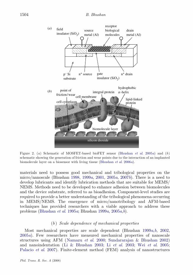
An example of a microarray-type biosensor (under development in ourlaboratory) is based on a field-effect transistor (FET) and is shown in figure 2a(Bhushan et al. 2005a; Lee et al. 2005a). In this sensor, the gate metal electrodeof a metal oxide semiconductor field effect transistor (MOSFET) is removed andreplaced with a protein (receptor layer) whose cognate is the analyte (e.g. virusor bacteria) that is meant to be sensed. The binding of the receptor layer with theanalyte produces a change in the effective charge which creates a change in theelectrical field. This electrical field change may produce a measurable change inthe current flow through the device. Adhesion between the protein layer andsilica substrate affects reliability of the biosensor. In the case of implantedbiosensors, the biosensors come in contact with the exterior environment such astissues and fluids, and any relative motion of the sensor surface with respect tothe exterior environment of tissues or fluids may result in surface damage(figure 2b; Bhushan et al. 2006a).
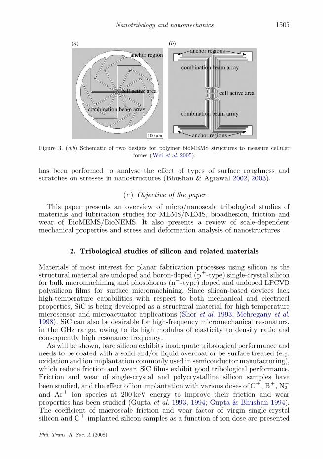
Polymer BioMEMS are designed to measure cellular surfaces. For twoexamples, see figure 3 (Wei et al. 2005). The device on the left shows cantileversanchored at the periphery of the circular structure, while that on the right hascantilevers anchored at the two corners on the top and the bottom. The celladheres to the centre of the structure, and the contractile forces generated in thecell’s cytoskeleton cause the cantilever to deflect. The deflection of the compliantpolymer cantilevers is measured optically and related to the magnitude of theforces generated by the cell. Adhesion between the cells and the polymer beam isdesirable. In order to design the sensors, micro- and nanoscale mechanicalproperties of polymer structures are needed.
Various MEMS/NEMS are designed to perform expected functions in themillisecond to picosecond range. The expected life of the devices for high-speedcontacts can vary from a few hundred thousand to many billions of cycles, e.g. overa hundred billion cycles for DMDs, which puts stringent requirements on materials.Adhesion between a biological molecular layer and the substrate, referred to as‘bioadhesion’, reduction of friction and wear of biological layers, biocompatibilityand biofouling for BioMEMS/BioNEMS are important. There is a need for thedevelopment of a fundamental understanding of adhesion, friction/stiction, wear,the role of surface contamination and environment (Bhushan 1998). MEMS/NEMS
Phil. Trans. R. Soc. A (2008)
fieldinsulator (SiO2)
gateinsulator (SiO2)
sourcemetal (Al)
receptorbiologicalmolecules
drainmetal (Al)
p– Sisubstrate
n+ source n+ drain
point offriction/wear
cell membraneintegral protein
hydrophobic -helix
lipid-linkedproteincell cytoplasm
biomolecule layer
silicon dioxide
(a)
(b)
Figure 2. (a) Schematic of MOSFET-based bioFET sensor (Bhushan et al. 2005a) and (b)schematic showing the generation of friction and wear points due to the interaction of an implantedbiomolecule layer on a biosensor with living tissue (Bhushan et al. 2006a).
B. Bhushan1504
materials need to possess good mechanical and tribological properties on themicro/nanoscale (Bhushan 1998, 1999a, 2001, 2005a, 2007b). There is a need todevelop lubricants and identify lubrication methods that are suitable for MEMS/NEMS. Methods need to be developed to enhance adhesion between biomoleculesand the device substrate, referred to as bioadhesion. Component-level studies arerequired to provide a better understanding of the tribological phenomena occurringin MEMS/NEMS. The emergence of micro/nanotribology and AFM-basedtechniques has provided researchers with a viable approach to address theseproblems (Bhushan et al. 1995a; Bhushan 1999a, 2005a,b).
(b ) Scale dependence of mechanical properties
Most mechanical properties are scale dependent (Bhushan 1999a,b, 2002,2005a). Few researchers have measured mechanical properties of nanoscalestructures using AFM (Namazu et al. 2000; Sundararajan & Bhushan 2002)and nanoindentation (Li & Bhushan 2003; Li et al. 2003; Wei et al. 2005;Palacio et al. 2007). Finite-element method (FEM) analysis of nanostructures
Phil. Trans. R. Soc. A (2008)
anchor regionanchor regions
anchor regions
cell active area cell active area
combination beam array
combination beam array
combination beam array
100 µm
(a) (b)
Figure 3. (a,b) Schematic of two designs for polymer bioMEMS structures to measure cellularforces (Wei et al. 2005).
1505Nanotribology and nanomechanics
has been performed to analyse the effect of types of surface roughness andscratches on stresses in nanostructures (Bhushan & Agrawal 2002, 2003).
(c ) Objective of the paper
This paper presents an overview of micro/nanoscale tribological studies ofmaterials and lubrication studies for MEMS/NEMS, bioadhesion, friction andwear of BioMEMS/BioNEMS. It also presents a review of scale-dependentmechanical properties and stress and deformation analysis of nanostructures.
2. Tribological studies of silicon and related materials
Materials of most interest for planar fabrication processes using silicon as thestructural material are undoped and boron-doped (pC-type) single-crystal siliconfor bulk micromachining and phosphorus (nC-type) doped and undoped LPCVDpolysilicon films for surface micromachining. Since silicon-based devices lackhigh-temperature capabilities with respect to both mechanical and electricalproperties, SiC is being developed as a structural material for high-temperaturemicrosensor and microactuator applications (Shor et al. 1993; Mehregany et al.1998). SiC can also be desirable for high-frequency micromechanical resonators,in the GHz range, owing to its high modulus of elasticity to density ratio andconsequently high resonance frequency.
As will be shown, bare silicon exhibits inadequate tribological performance andneeds to be coated with a solid and/or liquid overcoat or be surface treated (e.g.oxidation and ion implantation commonly used in semiconductor manufacturing),which reduce friction and wear. SiC films exhibit good tribological performance.Friction and wear of single-crystal and polycrystalline silicon samples have
been studied, and the effect of ion implantation with various doses of CC, BC, N2C
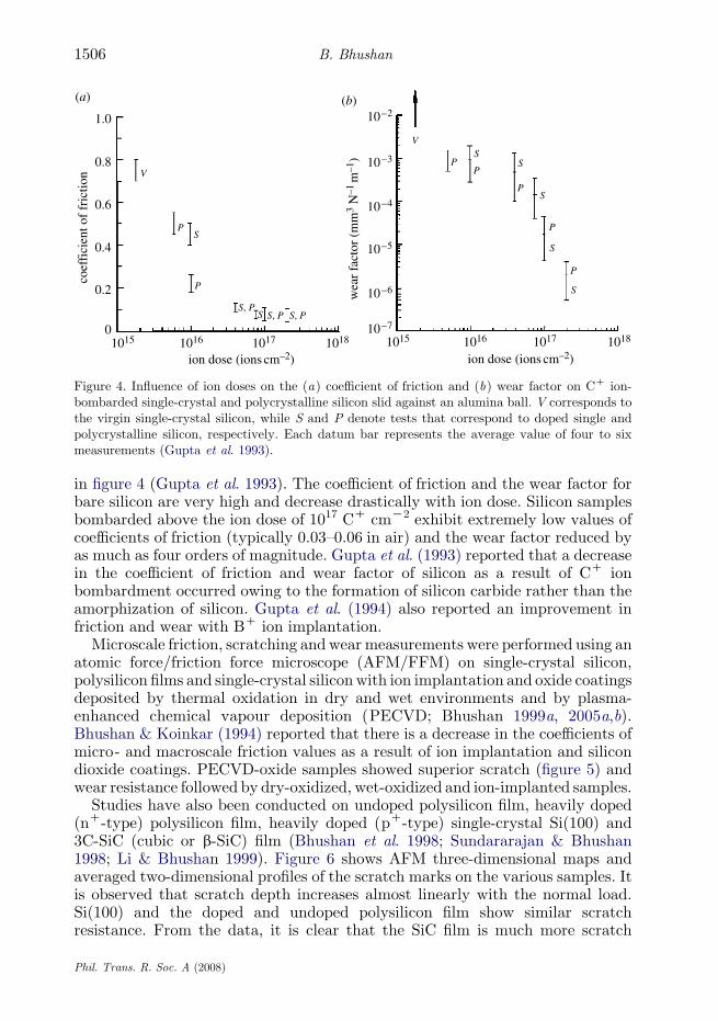
and ArC ion species at 200 keV energy to improve their friction and wearproperties has been studied (Gupta et al. 1993, 1994; Gupta & Bhushan 1994).The coefficient of macroscale friction and wear factor of virgin single-crystalsilicon and CC-implanted silicon samples as a function of ion dose are presented
Phil. Trans. R. Soc. A (2008)
coef
fici
ent o
f fr
ictio
n V
P
P
S
SS, P
S, P S, P
V
PP
P
P
P
SS
S
S
S
1.0
(a) (b)
0.8
0.6
0.4
0.2
0
ion dose (ions cm–2)1015 1016 1017 1018
ion dose (ions cm–2)1015 1016 1017 1018
10–7
10–6
10–5
10–4
10–3
10–2
wea
r fa
ctor
(m
m3
N–1
m–1
)
Figure 4. Influence of ion doses on the (a) coefficient of friction and (b) wear factor on CC ion-bombarded single-crystal and polycrystalline silicon slid against an alumina ball. V corresponds tothe virgin single-crystal silicon, while S and P denote tests that correspond to doped single andpolycrystalline silicon, respectively. Each datum bar represents the average value of four to sixmeasurements (Gupta et al. 1993).
B. Bhushan1506
in figure 4 (Gupta et al. 1993). The coefficient of friction and the wear factor forbare silicon are very high and decrease drastically with ion dose. Silicon samplesbombarded above the ion dose of 1017 CC cmK2 exhibit extremely low values ofcoefficients of friction (typically 0.03–0.06 in air) and the wear factor reduced byas much as four orders of magnitude. Gupta et al. (1993) reported that a decreasein the coefficient of friction and wear factor of silicon as a result of CC ionbombardment occurred owing to the formation of silicon carbide rather than theamorphization of silicon. Gupta et al. (1994) also reported an improvement infriction and wear with BC ion implantation.
Microscale friction, scratching and wearmeasurements were performed using anatomic force/friction force microscope (AFM/FFM) on single-crystal silicon,polysilicon films and single-crystal siliconwith ion implantation and oxide coatingsdeposited by thermal oxidation in dry and wet environments and by plasma-enhanced chemical vapour deposition (PECVD; Bhushan 1999a, 2005a,b).Bhushan & Koinkar (1994) reported that there is a decrease in the coefficients ofmicro- and macroscale friction values as a result of ion implantation and silicondioxide coatings. PECVD-oxide samples showed superior scratch (figure 5) andwear resistance followed by dry-oxidized, wet-oxidized and ion-implanted samples.
Studies have also been conducted on undoped polysilicon film, heavily doped(nC-type) polysilicon film, heavily doped (pC-type) single-crystal Si(100) and3C-SiC (cubic or b-SiC) film (Bhushan et al. 1998; Sundararajan & Bhushan1998; Li & Bhushan 1999). Figure 6 shows AFM three-dimensional maps andaveraged two-dimensional profiles of the scratch marks on the various samples. Itis observed that scratch depth increases almost linearly with the normal load.Si(100) and the doped and undoped polysilicon film show similar scratchresistance. From the data, it is clear that the SiC film is much more scratch
Phil. Trans. R. Soc. A (2008)
250
200
150
100
50
0 20 40 60 80 100normal load (µN)
scra
tch
dept
h (n
m)
Figure 5. Scratch depth as a function of normal load after 10 cycles for various silicon samples,virgin, treated and coated (Bhushan & Koinkar 1994). Open circle, undoped Si(100); closed circle,PECVD-oxide Si(111); open triangle, dry-oxidized Si(111); closed triangle, wet-oxidized Si(111);open square, CC-implanted Si(111).
1507Nanotribology and nanomechanics
resistant than the other samples. Wear experiments showed the same trends.These studies indicate that SiC film exhibits desirable tribological properties foruse in MEMS devices.
3. Lubrication studies for MEMS/NEMS
Several studies of liquid perfluoropolyether (PFPE) lubricant films and SAMshave been carried out for the purpose of minimizing adhesion, friction and wear(Bhushan et al. 1995b, 2005b, 2006b,c; Koinkar & Bhushan 1996a,b; Henck 1997;Bhushan 1999a,c, 2005a,b; Bhushan & Liu 2001; Liu & Bhushan 2002, 2003;Kasai et al. 2005; Lee et al. 2005b; Tambe & Bhushan 2005; Tao & Bhushan2005a,b). Many variations of these films are hydrophobic (low surface tensionand high contact angle) and have low shear strength which provide low adhesion,friction and wear.
The classical approach to lubrication uses freely supported multimolecularlayers of liquid lubricants (Bhushan 1999a,b, 2002, 2005a). The liquid lubricantsare sometimes chemically bonded to improve their wear resistance. Partiallychemically bonded, molecularly thick PFPE lubricants are widely used forlubrication of magnetic storage media, owing to their thermal stability andextremely low vapour pressure (Bhushan 1996), and are found to be suitable forMEMS/NEMS devices. Adhesion, friction and durability experiments have beenperformed on virgin Si(100) and silicon surfaces lubricated with two commonlyused PFPE lubricants—Z-15 (with –CF3 non-polar end groups) and Z-DOL(with –OH polar end groups; Koinkar & Bhushan 1996a,b; Bhushan 1999a,2005a; Liu & Bhushan 2003; Tao & Bhushan 2005a; Bhushan et al. 2006b,c). Theadhesive forces of Si(100), Z-15 and Z-DOL (BW) measured by two methods aresummarized in figure 7. The figure shows that the presence of mobile Z-15lubricant film increases the adhesive force when compared with that of Si(100)by meniscus formation (Bhushan 1999b, 2002), whereas the presence of solid-phase Z-DOL (BW) film reduces the adhesive force when compared with that of
Phil. Trans. R. Soc. A (2008)
100
100
100
100
80
80
80
80
60
60
60
60
40
40
40
40
20 µN
20 µN
20 µN
20 µN
5.00
5.00
5.00
5.00
2.50
2.50
2.50
2.50
0 –200
0
200
–200
0
200
–200
0
200
–200
0
0
100 80 60 40 20 µN
100 80 60 40 20 µN
100 80 60 40 20 µN
2.50 5.00 µm
200
100 80 60 40 20 µN
0
0
0
2.505.00
0 µm
0 µm
0 µm
0 µm
750
750
750
750
500
500
500
500
250
250
250
250
nm
nm
nm
nm
nm
nm
nm
nm
(a)
(b)
(c)
(d )
Figure 6. AFM three-dimensional maps and averaged two-dimensional profiles of scratch markson various samples (Bhushan et al. 1998). (a) Undoped Si(100), (b) undoped polysilicon film,(c ) nC-type polysilicon film and (d ) SiC film.
B. Bhushan1508
Phil. Trans. R. Soc. A (2008)
100(a)
(b)
75
50
adhe
sive
for
ce (
nN)
25
0Si(100)
Si(100)
Z-15
Z-15
Z-15
Z-DOL (BW)
Z-DOL (BW)
Z-DOL
22°C, RH 45–55%
–O–Si–O–
– –O
–
H2O
Figure 7. (a ) Summary of the adhesive forces of Si(100) and Z-15 (2.8 nm film thickness) andZ-DOL (bonded washed, BW; 2.3 nm film thickness) films measured by force calibration plots andfriction force versus normal load plots in ambient air. Open bars, force calibration plot; slashedbars, friction force plot. (b) The schematic showing the effect of meniscus, formed between theAFM tip and the surface sample, on the adhesive and friction forces (Liu & Bhushan 2003).
1509Nanotribology and nanomechanics
Si(100) owing to the absence of mobile liquid. Figure 7b shows the relative sizeand sources of meniscus. It is well known that the native oxide layer (SiO2) onthe top of the Si(100) wafer exhibits hydrophilic properties, and some watermolecules can be adsorbed on this surface. The condensed water will form ameniscus as the tip approaches the sample surface. The larger adhesive force inZ-15 is not just caused by the Z-15 meniscus, and the non-polarized Z-15 liquiddoes not have good wettability and strong bonding with Si(100). Consequently,in the ambient environment, the condensed water molecules from theenvironment permeate through the liquid Z-15 lubricant film and competewith the lubricant molecules presented on the substrate. The interaction of theliquid lubricant with the substrate is weakened, and a boundary layer of theliquid lubricant forms puddles (Koinkar & Bhushan 1996a,b). This dewettingallows water molecules to be adsorbed on the Si(100) surface as aggregatesalong with Z-15 molecules. And both of them can form a meniscus while the tipapproaches the surface. Thus, the dewetting of liquid Z-15 film results in higheradhesive force and poorer lubrication performance.
For lubrication of MEMS/NEMS, another effective approach involves thedeposition of organized and dense molecular layers of long-chain molecules,referred to as SAMs, by chemical grafting of molecules (Bhushan et al. 1995b,2005b, 2006b,c; Bhushan & Liu 2001; Liu et al. 2001; Liu & Bhushan 2002;Kasai et al. 2005; Lee et al. 2005b; Tambe & Bhushan 2005; Tao & Bhushan
Phil. Trans. R. Soc. A (2008)
n-dimethyl(dimethylamino)silaneocta (ODMS) octadecyl (ODDMS)
perfluorodecyltrichlorosilanedeca (PFTS)
n-phosphonateoctadecyl (ODP)decyl (DP)
perfluorodecylphosphonatedeca (PFDP)
CH3
CH3
CH3
CF3(CH2)17
(CH2)2
(CF2)7(CH2)9
(CH2)17(CF2)7(CH2)2
(CH2)7
CF3CH3
CH3–Si–CH3
––
––
O
–Si––––
CH3–Si–CH3
––
––
O
–Si––––
–O–Si–O–
––
––
O
–Si––––
–O–P–O
––
––
O
–Al––––
– –O–P–O
––
––
O
–Al––––
– –O–P–O
––
––
O
–Al––––
–
Figure 8. Schematics of structures of perfluoroalkylsilane and alkylsilane SAMs on Si withnative oxide substrates, and alkylphosphonate and perfluoroalkylphosphonate SAMs on Al withnative oxide.
B. Bhushan1510
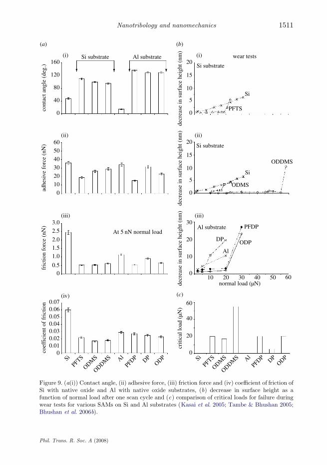
2005b). Bhushan et al. (2005b), Kasai et al. (2005), Tambe & Bhushan (2005) andBhushan et al. (2006b) studied perfluorodecyltrichlorosilane (PFTS), n-octyldi-methyl (dimethylamino) silane (ODMS; nZ7) and n-octadecylmethyl (dimethyl-amino) silane (ODDMS) (nZ17) vapour phase deposited on Si substrate, anddecylphosphonate (DP), octadecylphosphonate (ODP) and perfluorodecylphos-phonate (PFDP) on Al substrate (figure 8). Figure 9a presents the contact angle,adhesive force, friction force and coefficient of friction of two substrates and withvarious SAMs. Based on the data, PFTS/Si exhibits a higher contact angle andlower adhesive force when compared with that of ODMS/Si and ODDMS/Si.Data of various films on Si substrate are similar to those of the correspondingvarious films on Al substrate. Thus substrate had little effect. The coefficient offriction of various SAMs was comparable. For wear performance studies,experiments were conducted on various films. Figure 9b shows the relationshipbetween the decrease in surface height and the normal load for various SAMs andcorresponding substrates (Kasai et al. 2005; Tambe & Bhushan 2005; Bhushanet al. 2006b). As shown in the figure, the SAMs exhibit a critical normal loadbeyond which point the surface height drastically decreases. Unlike SAMs, thesubstrates show a monotonic decrease in surface height with increasing normalload with wear initiating from the very beginning, i.e. even for low normalloads. The critical loads corresponding to the sudden failure are shown infigure 9c. Out of the two alkyl SAMs, ODDMS/Si and ODP/Al show a betterwear resistance than ODMS/Si and DP/Al due to the chain length effect. Wearbehaviour of the SAMs is reported to be mostly determined by the molecule–substrate bond strengths.
4. Tribological studies of biological molecules on silicon-based andpolymer surfaces
Proteins on silicon-based surfaces are of extreme importance in variousapplications including silicon microimplants, various bioMEMS, such asbiosensors, and therapeutics. Silicon is a commonly used substrate inmicroimplants, but it can have undesired interactions with the human immunesystem. Therefore, to mimic a biological surface, protein coatings are used on
Phil. Trans. R. Soc. A (2008)
Si
coef
fici
ent o
f fr
ictio
n
PFTS
ODMS
ODDMS Al
PFDP DPODP Si
PFTS
ODMS
ODDMS Al
PFDP DPODP
0
00.5
1.01.52.0
2.5
3.0
0
10
20
30
40
50
60
0
40
80
120
160
(a)
(i)
(ii)
(iii)
(i)
(ii)
(iii)
(iv)
(b)
(c)
0.010.020.030.040.050.060.07
Si substrate Al substrate
At 5 nN normal load
wear tests
Si substrate
Si
PFTS
decr
ease
in s
urfa
ce h
eigh
t (nm
)
20
15
10
5
0
20
15
10
5
0
30
20
10
0
0
20
40
60
10 20 30normal load (µN)
40 50 60
cont
act a
ngle
(de
g.)
adhe
sive
for
ce (
nN)
fric
tion
forc
e (n
N)
criti
cal l
oad
(µN
)de
crea
se in
sur
face
hei
ght (
nm)
decr
ease
in s
urfa
ce h
eigh
t (nm
)
Al substrate
Si substrate
DP
Al
ODP
PFDP
ODDMS
ODMS
Si
Figure 9. (a(i)) Contact angle, (ii) adhesive force, (iii) friction force and (iv) coefficient of friction ofSi with native oxide and Al with native oxide substrates, (b) decrease in surface height as afunction of normal load after one scan cycle and (c ) comparison of critical loads for failure duringwear tests for various SAMs on Si and Al substrates (Kasai et al. 2005; Tambe & Bhushan 2005;Bhushan et al. 2006b).
1511Nanotribology and nanomechanics
Phil. Trans. R. Soc. A (2008)
B. Bhushan1512
silicon-based surfaces as passivation layers, so that these implants are compatiblein the body and avoid rejection. Whether this surface treatment is applied to alarge implant or to a bioMEMS, the function of the protein passivation isobtained from the nanoscale three-dimensional structural conformation of theprotein. Proteins are also used in bioMEMS owing to their function specificity.For biosensor applications, the extensive array of protein activities provides arich supply of operations that may be performed at the nanoscale. Manyantibodies (proteins) have an affinity to specific protein antigens. For example,pathogens (disease-causing agents, e.g. virus or bacteria) trigger production ofantigens which can be detected when bound to a specific antibody on thebiosensor. The specific binding behaviour of proteins, which has been applied tothe laboratory assays, may also be redesigned for in vivo use as sensing elementsof a bioMEMS. The epitope-specific binding properties of proteins to variousantigens are useful in therapeutics. Adhesion between the protein and substrateaffects the reliability of an application. Among other things, morphology of thesubstrate affects the adhesion. Furthermore, for in vivo environments, theproteins on the biosensor surface should exhibit high wear resistance duringthe direct contact with the tissue and circulatory blood flow without washing off.
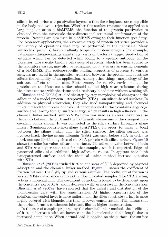
Bhushan et al. (2005a) studied the step-by-step morphological changes and theadhesion of a model protein—streptavidin (STA)—on silicon-based surfaces. Inaddition to physical adsorption, they also used nanopatterning and chemicallinker methods to improve adhesion. A nanopatterned surface contains large edgesurface area leading to high surface energy, which results in high adhesion. In thechemical linker method, sulpho-NHS-biotin was used as a cross linker becausethe bonds between the STA and the biotin molecule are one of the strongest non-covalent bonds known. It was connected to the silica surface through a silanelinker, 3-aminopropyltriethoxysilane (3-APTES). In order to make a bondbetween the silane linker and the silica surface, the silica surface washydroxylated. Bovine serum albumin (BSA) was used before STA in order toblock non-specific binding sites of the STA protein with silica surface. Figure 10shows the adhesion values of various surfaces. The adhesion value between biotinand STA was higher than that for other samples, which is expected. Edges ofpatterned silica also exhibited high adhesion values. It appears that bothnanopatterned surfaces and the chemical linker method increase adhesionwith STA.
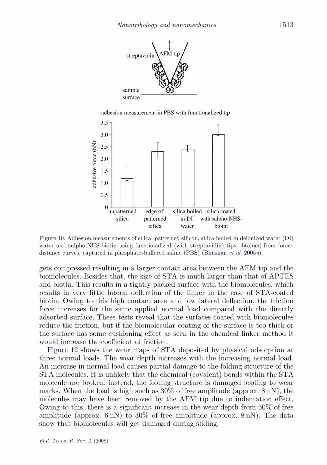
Bhushan et al. (2006a) studied friction and wear of STA deposited by physicaladsorption and the chemical linker method. Figure 11 shows the coefficient offriction between the Si3N4 tip and various samples. The coefficient of friction isless for STA-coated silica samples than for uncoated samples. The STA coatingacts as a lubricant film. The coefficient of friction is found to be dependent uponthe concentration of STA, and it decreases with an increase in the concentration.Bhushan et al. (2005a) have reported that the density and distribution of thebiomolecules vary with the concentration. At higher concentration of thesolution, the coated layer is more uniform and the silica substrate surface is morehighly covered with biomolecules than at lower concentration. This means thatthe surface forms a continuous lubricant film at higher concentration.
In the case of samples prepared by the chemical linker method, the coefficientof friction increases with an increase in the biomolecular chain length due toincreased compliance. When normal load is applied on the surface, the surface
Phil. Trans. R. Soc. A (2008)
samplesurface
streptavidin AFM tip
adhesion measurement in PBS with functionalized tip
3.5
3.0
2.5
2.0
1.5
1.0
0.5
0
adhe
sive
for
ce (
nN)
unpatternedsilica
edge of patterned
silica
silica boiledin DI water
silica coatedwith sulpho-NHS-
biotin
Figure 10. Adhesion measurements of silica, patterned silicon, silica boiled in deionized water (DI)water and sulpho-NHS-biotin using functionalized (with streptavidin) tips obtained from force–distance curves, captured in phosphate-buffered saline (PBS) (Bhushan et al. 2005a).
1513Nanotribology and nanomechanics
gets compressed resulting in a larger contact area between the AFM tip and thebiomolecules. Besides that, the size of STA is much larger than that of APTESand biotin. This results in a tightly packed surface with the biomolecules, whichresults in very little lateral deflection of the linker in the case of STA-coatedbiotin. Owing to this high contact area and low lateral deflection, the frictionforce increases for the same applied normal load compared with the directlyadsorbed surface. These tests reveal that the surfaces coated with biomoleculesreduce the friction, but if the biomolecular coating of the surface is too thick orthe surface has some cushioning effect as seen in the chemical linker method itwould increase the coefficient of friction.
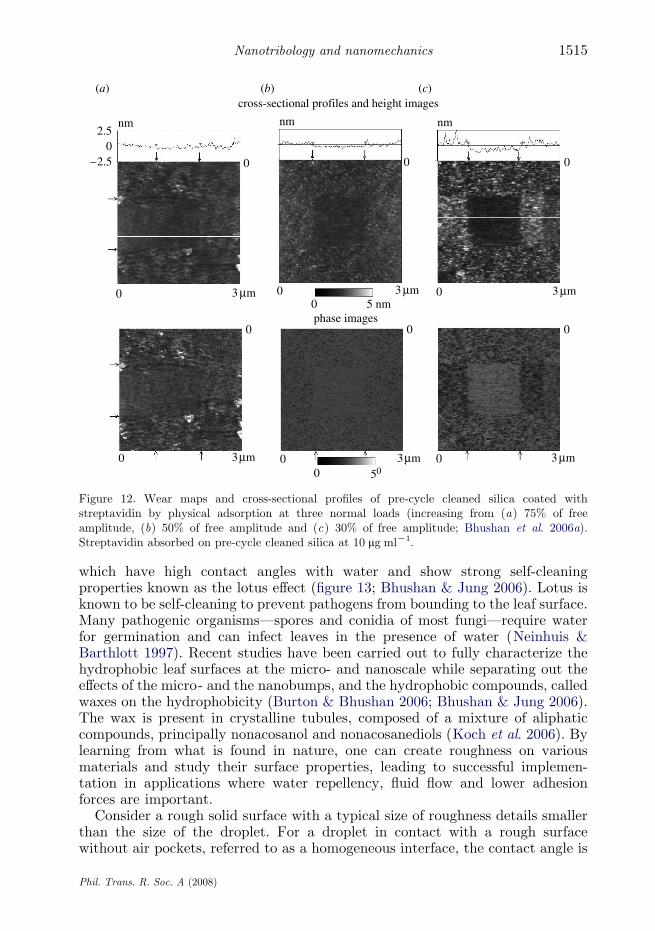
Figure 12 shows the wear maps of STA deposited by physical adsorption atthree normal loads. The wear depth increases with the increasing normal load.An increase in normal load causes partial damage to the folding structure of theSTA molecules. It is unlikely that the chemical (covalent) bonds within the STAmolecule are broken; instead, the folding structure is damaged leading to wearmarks. When the load is high such as 30% of free amplitude (approx. 8 nN), themolecules may have been removed by the AFM tip due to indentation effect.Owing to this, there is a significant increase in the wear depth from 50% of freeamplitude (approx. 6 nN) to 30% of free amplitude (approx. 8 nN). The datashow that biomolecules will get damaged during sliding.
Phil. Trans. R. Soc. A (2008)
101 100
0.04
0.03
0.02
0.01
0
coef
fici
ent o
f fr
ictio
n
pre-
cycl
ecl
eane
d si
lica
STA by adsorptionat µg ml–1 si
lani
zed
silic
a
NH
S-bi
otin
-co
ated
sili
ca
STA
by
chem
ical
linke
r at
10
µgm
l–1
Figure 11. Coefficient of friction for various surfaces with and without biomolecules (Bhushan et al.2006a).
B. Bhushan1514
5. Nanopatterned surfaces
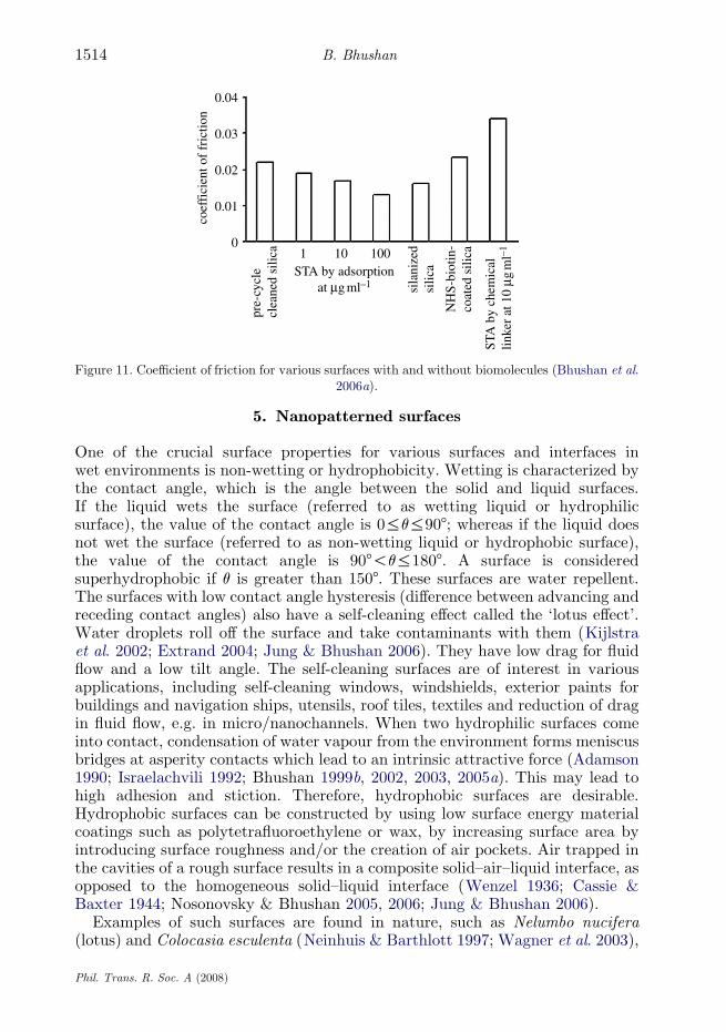
One of the crucial surface properties for various surfaces and interfaces inwet environments is non-wetting or hydrophobicity. Wetting is characterized bythe contact angle, which is the angle between the solid and liquid surfaces.If the liquid wets the surface (referred to as wetting liquid or hydrophilicsurface), the value of the contact angle is 0%q%908; whereas if the liquid doesnot wet the surface (referred to as non-wetting liquid or hydrophobic surface),the value of the contact angle is 908!q%1808. A surface is consideredsuperhydrophobic if q is greater than 1508. These surfaces are water repellent.The surfaces with low contact angle hysteresis (difference between advancing andreceding contact angles) also have a self-cleaning effect called the ‘lotus effect’.Water droplets roll off the surface and take contaminants with them (Kijlstraet al. 2002; Extrand 2004; Jung & Bhushan 2006). They have low drag for fluidflow and a low tilt angle. The self-cleaning surfaces are of interest in variousapplications, including self-cleaning windows, windshields, exterior paints forbuildings and navigation ships, utensils, roof tiles, textiles and reduction of dragin fluid flow, e.g. in micro/nanochannels. When two hydrophilic surfaces comeinto contact, condensation of water vapour from the environment forms meniscusbridges at asperity contacts which lead to an intrinsic attractive force (Adamson1990; Israelachvili 1992; Bhushan 1999b, 2002, 2003, 2005a). This may lead tohigh adhesion and stiction. Therefore, hydrophobic surfaces are desirable.Hydrophobic surfaces can be constructed by using low surface energy materialcoatings such as polytetrafluoroethylene or wax, by increasing surface area byintroducing surface roughness and/or the creation of air pockets. Air trapped inthe cavities of a rough surface results in a composite solid–air–liquid interface, asopposed to the homogeneous solid–liquid interface (Wenzel 1936; Cassie &Baxter 1944; Nosonovsky & Bhushan 2005, 2006; Jung & Bhushan 2006).
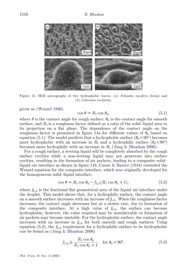
Examples of such surfaces are found in nature, such as Nelumbo nucifera(lotus) and Colocasia esculenta (Neinhuis & Barthlott 1997; Wagner et al. 2003),
Phil. Trans. R. Soc. A (2008)
cross-sectional profiles and height images
2.5
–2.5
nm nm nm
5 nm
50
0
0
0
0 0 0
00
00
0
0
0 0 0
3 µm
3µm
3 µm
3µm
3 µm
3 µm
phase images
(a) (b) (c)
Figure 12. Wear maps and cross-sectional profiles of pre-cycle cleaned silica coated withstreptavidin by physical adsorption at three normal loads (increasing from (a) 75% of freeamplitude, (b) 50% of free amplitude and (c) 30% of free amplitude; Bhushan et al. 2006a).Streptavidin absorbed on pre-cycle cleaned silica at 10 mg mlK1.
1515Nanotribology and nanomechanics
which have high contact angles with water and show strong self-cleaningproperties known as the lotus effect (figure 13; Bhushan & Jung 2006). Lotus isknown to be self-cleaning to prevent pathogens from bounding to the leaf surface.Many pathogenic organisms—spores and conidia of most fungi—require waterfor germination and can infect leaves in the presence of water (Neinhuis &Barthlott 1997). Recent studies have been carried out to fully characterize thehydrophobic leaf surfaces at the micro- and nanoscale while separating out theeffects of the micro- and the nanobumps, and the hydrophobic compounds, calledwaxes on the hydrophobicity (Burton & Bhushan 2006; Bhushan & Jung 2006).The wax is present in crystalline tubules, composed of a mixture of aliphaticcompounds, principally nonacosanol and nonacosanediols (Koch et al. 2006). Bylearning from what is found in nature, one can create roughness on variousmaterials and study their surface properties, leading to successful implemen-tation in applications where water repellency, fluid flow and lower adhesionforces are important.
Consider a rough solid surface with a typical size of roughness details smallerthan the size of the droplet. For a droplet in contact with a rough surfacewithout air pockets, referred to as a homogeneous interface, the contact angle is
Phil. Trans. R. Soc. A (2008)
5 µm 5 µm
20 µm20 µm
(a) (b)
Figure 13. SEM micrographs of two hydrophobic leaves, (a) Nelumbo nucifera (lotus) and(b) Colocasia esculenta.
B. Bhushan1516
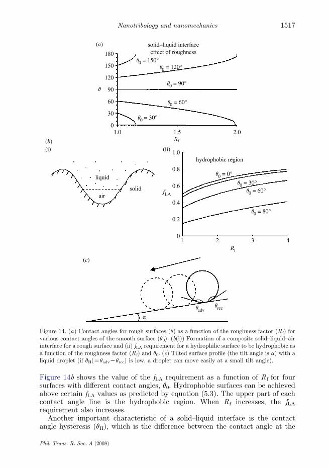
given as (Wenzel 1936)cos qZR f cos q0; ð5:1Þ
where q is the contact angle for rough surface; q0 is the contact angle for smoothsurface; and Rf is a roughness factor defined as a ratio of the solid–liquid area toits projection on a flat plane. The dependence of the contact angle on theroughness factor is presented in figure 14a for different values of q0 based onequation (5.1). The model predicts that a hydrophobic surface (q0O908) becomesmore hydrophobic with an increase in Rf and a hydrophilic surface (q0!908)becomes more hydrophilic with an increase in Rf (Jung & Bhushan 2006).
For a rough surface, a wetting liquid will be completely absorbed by the roughsurface cavities while a non-wetting liquid may not penetrate into surfacecavities, resulting in the formation of air pockets, leading to a composite solid–liquid–air interface as shown in figure 14b. Cassie & Baxter (1944) extended theWenzel equation for the composite interface, which was originally developed forthe homogeneous solid–liquid interface,
cos qZR f cos q0K f LAðR f cos q0C1Þ; ð5:2Þwhere fLA is the fractional flat geometrical area of the liquid–air interface underthe droplet. This model shows that, for a hydrophilic surface, the contact angleon a smooth surface increases with an increase of fLA. When the roughness factorincreases, the contact angle decreases but at a slower rate, due to formation ofthe composite interface. At a high value of fLA, the surface can becomehydrophobic; however, the value required may be unachievable or formation ofair pockets may become unstable. For the hydrophobic surface, the contact angleincreases with an increase in fLA for both smooth and rough surfaces. Usingequation (5.2), the fLA requirement for a hydrophilic surface to be hydrophobiccan be found as (Jung & Bhushan 2006)
f LARR f cos q0
R f cos q0 C1for q0!908: ð5:3Þ
Phil. Trans. R. Soc. A (2008)
180
150
120
90
60
30
01.0 1.5 2.0
0 = 30°
(a)
liquid
airsolid
1.0
0.8
0.6
0.4
0.2
01 2 3 4
Rf
(b)
adv rec
(c)
hydrophobic region
fLA
solid–liquid interfaceeffect of roughness
(i) (ii)
0 = 60°
0 = 60°
0 = 80°
0 = 30°0 = 0°
0 = 90°
0 = 120°0 = 150°
Figure 14. (a) Contact angles for rough surfaces (q) as a function of the roughness factor (Rf) forvarious contact angles of the smooth surface (q0). (b(i)) Formation of a composite solid–liquid–airinterface for a rough surface and (ii) fLA requirement for a hydrophilic surface to be hydrophobic asa function of the roughness factor (Rf) and q0. (c) Tilted surface profile (the tilt angle is a) with aliquid droplet (if qH(ZqadvKqrec) is low, a droplet can move easily at a small tilt angle).
1517Nanotribology and nanomechanics
Figure 14b shows the value of the fLA requirement as a function of Rf for foursurfaces with different contact angles, q0. Hydrophobic surfaces can be achievedabove certain fLA values as predicted by equation (5.3). The upper part of eachcontact angle line is the hydrophobic region. When Rf increases, the fLArequirement also increases.
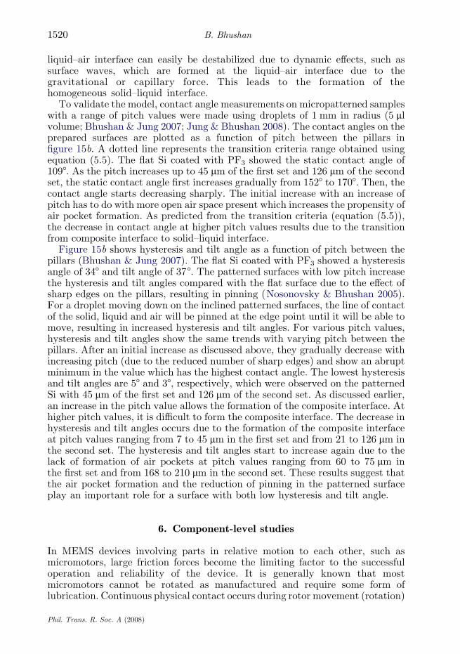
Another important characteristic of a solid–liquid interface is the contactangle hysteresis (qH), which is the difference between the contact angle at the
Phil. Trans. R. Soc. A (2008)
B. Bhushan1518
increased droplet volume (advancing contact angle, qadv) and the contact angleat the decreased droplet volume (receding contact angle, qrec) for a droplet on thesolid surface. The contact angle hysteresis occurs due to surface roughness andheterogeneity. Low contact angle hysteresis results in a very low water roll-offangle, which denotes the angle to which a surface may be tilted for roll off ofwater drops (Kijlstra et al. 2002; Extrand 2004). Low water roll-off angle isimportant in liquid flow applications such as in micro/nanochannels and surfaceswith self-cleaning ability.
There is no simple expression for the contact angle hysteresis as a functionof roughness; however, certain conclusions about the relation of the contact anglehysteresis to roughness can be made. In the limiting case of very small solid–liquid fractional contact area under the droplet, when the contact angle is largeand the contact angle hysteresis is small, equation (5.2) is reduced to
qadvK qrec Zffiffiffiffiffiffiffiffiffiffiffiffiffiffiffiffi1K f LA
pR f
cos qr 0Kcos qa0ffiffiffiffiffiffiffiffiffiffiffiffiffiffiffiffiffiffiffiffiffiffiffiffiffiffiffiffiffiffiffiffiffiffi2ðR f cos q0 C1Þ
p : ð5:4Þ
For the homogeneous interface, fLAZ0,whereas for the composite interface fLA isnot zero. It is observed from equation (5.4) that, for the homogeneous interface,increasing roughness (high Rf) leads to increasing the contact angle hysteresis,while, for the composite interface, an approach to unity of fLA provides bothhigh contact angle and small contact angle hysteresis (Jung & Bhushan 2006;Bhushan et al. 2007). Therefore, the composite interface is desirable forsuperhydrophobicity.
Formation of a composite interface is also a multiscale phenomenon, whichdepends upon the relative sizes of the liquid droplet and roughness details.A stable composite interface is essential for the successful design of super-hydrophobic surfaces. However, the composite interface is fragile and itmay transform into the homogeneous interface. Nosonovsky & Bhushan(2007a) have studied destabilizing factors for the composite interface andfound that the sign of the surface curvature is important, especially in the caseof multiscale (hierarchical) roughness. A convex surface (with bumps) leads to astable interface and high contact angle. Also, they have suggested that theeffects of a droplet’s weight and curvature are among the factors which affectthe transition.
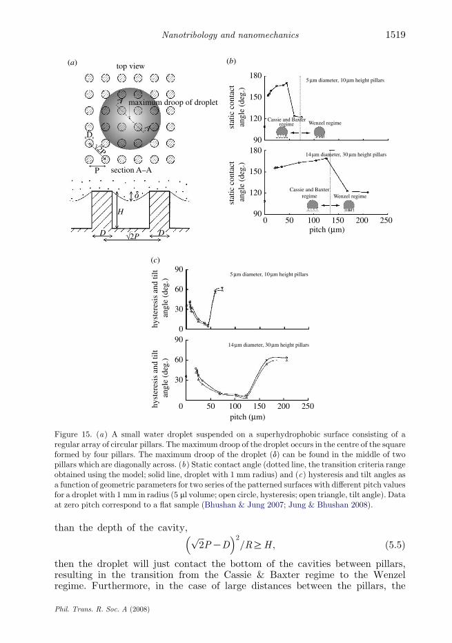
Jung & Bhushan (2008) developed the model to predict the transition fromthe Cassie & Baxter regime to the Wenzel regime based on the factorsdiscussed above. First, they considered a small water droplet suspended on asuperhydrophobic surface consisting of a regular array of circular pillars withdiameter D, height H and pitch P. The local deformation for small droplets isgoverned by surface effects rather than gravity. The curvature of a droplet isgoverned by the Laplace equation that relates the pressure inside the dropletto its curvature (Adamson 1990). The curvature is the same at the top and atthe bottom of the droplet (Lafuma & Quere 2003; Nosonovsky & Bhushan2007b). For the patterned surface considered here, the maximum droop of thedroplet occurs in the centre of the square formed by the four pillars as shownin figure 15a. Therefore, the maximum droop of the droplet (d) in the recessedregion can be found in the middle of two pillars that are diagonally across asshown in figure 15a, which is ð
ffiffiffi2
pPKD Þ2=ð8RÞ. If the droop is much greater
Phil. Trans. R. Soc. A (2008)
top view
maximum droop of dropletA
AD
D D
P
2P
section A–A
√
2P√
180
180
150
150
120
120
90
90
90
90
60
60
30
30
0
0
0 50
50
100
100
150
150
200
200
250
250
Cassie and Baxterregime
Cassie and Baxterregime
Wenzel regime
Wenzel regime
5 µm diameter, 10 µm height pillars
14 µm diameter, 30 µm height pillars
5 µm diameter, 10 µm height pillars
14 µm diameter, 30 µm height pillars
stat
ic c
onta
ctan
gle
(deg
.)st
atic
con
tact
ang
le (
deg.
)
pitch (µm)
pitch (µm)
hyst
eres
is a
nd ti
lt a
ngle
(de
g.)
hyst
eres
is a
nd ti
lt a
ngle
(de
g.)
H
(a) (b)
(c)
Figure 15. (a) A small water droplet suspended on a superhydrophobic surface consisting of aregular array of circular pillars. The maximum droop of the droplet occurs in the centre of the squareformed by four pillars. The maximum droop of the droplet (d) can be found in the middle of twopillars which are diagonally across. (b) Static contact angle (dotted line, the transition criteria rangeobtained using the model; solid line, droplet with 1 mm radius) and (c) hysteresis and tilt angles asa function of geometric parameters for two series of the patterned surfaces with different pitch valuesfor a droplet with 1 mm in radius (5 ml volume; open circle, hysteresis; open triangle, tilt angle). Dataat zero pitch correspond to a flat sample (Bhushan & Jung 2007; Jung & Bhushan 2008).
1519Nanotribology and nanomechanics
than the depth of the cavity, ffiffiffi2
pPKD
� �2=RRH ; ð5:5Þ
then the droplet will just contact the bottom of the cavities between pillars,resulting in the transition from the Cassie & Baxter regime to the Wenzelregime. Furthermore, in the case of large distances between the pillars, the
Phil. Trans. R. Soc. A (2008)
B. Bhushan1520
liquid–air interface can easily be destabilized due to dynamic effects, such assurface waves, which are formed at the liquid–air interface due to thegravitational or capillary force. This leads to the formation of thehomogeneous solid–liquid interface.
To validate the model, contact angle measurements on micropatterned sampleswith a range of pitch values were made using droplets of 1 mm in radius (5 mlvolume; Bhushan & Jung 2007; Jung & Bhushan 2008). The contact angles on theprepared surfaces are plotted as a function of pitch between the pillars infigure 15b. A dotted line represents the transition criteria range obtained usingequation (5.5). The flat Si coated with PF3 showed the static contact angle of1098. As the pitch increases up to 45 mm of the first set and 126 mm of the secondset, the static contact angle first increases gradually from 1528 to 1708. Then, thecontact angle starts decreasing sharply. The initial increase with an increase ofpitch has to do with more open air space present which increases the propensity ofair pocket formation. As predicted from the transition criteria (equation (5.5)),the decrease in contact angle at higher pitch values results due to the transitionfrom composite interface to solid–liquid interface.
Figure 15b shows hysteresis and tilt angle as a function of pitch between thepillars (Bhushan & Jung 2007). The flat Si coated with PF3 showed a hysteresisangle of 348 and tilt angle of 378. The patterned surfaces with low pitch increasethe hysteresis and tilt angles compared with the flat surface due to the effect ofsharp edges on the pillars, resulting in pinning (Nosonovsky & Bhushan 2005).For a droplet moving down on the inclined patterned surfaces, the line of contactof the solid, liquid and air will be pinned at the edge point until it will be able tomove, resulting in increased hysteresis and tilt angles. For various pitch values,hysteresis and tilt angles show the same trends with varying pitch between thepillars. After an initial increase as discussed above, they gradually decrease withincreasing pitch (due to the reduced number of sharp edges) and show an abruptminimum in the value which has the highest contact angle. The lowest hysteresisand tilt angles are 58 and 38, respectively, which were observed on the patternedSi with 45 mm of the first set and 126 mm of the second set. As discussed earlier,an increase in the pitch value allows the formation of the composite interface. Athigher pitch values, it is difficult to form the composite interface. The decrease inhysteresis and tilt angles occurs due to the formation of the composite interfaceat pitch values ranging from 7 to 45 mm in the first set and from 21 to 126 mm inthe second set. The hysteresis and tilt angles start to increase again due to thelack of formation of air pockets at pitch values ranging from 60 to 75 mm inthe first set and from 168 to 210 mm in the second set. These results suggest thatthe air pocket formation and the reduction of pinning in the patterned surfaceplay an important role for a surface with both low hysteresis and tilt angle.
6. Component-level studies
In MEMS devices involving parts in relative motion to each other, such asmicromotors, large friction forces become the limiting factor to the successfuloperation and reliability of the device. It is generally known that mostmicromotors cannot be rotated as manufactured and require some form oflubrication. Continuous physical contact occurs during rotor movement (rotation)
Phil. Trans. R. Soc. A (2008)
unlubricated
25
20
15
10
5
0
rotor
mobileliquid lubricant
hub
norm
aliz
edst
atic
fri
ctio
n fo
rce
motorM1 M2
bonded liquidlubricant
Figure 16. Summary of the effect of liquid and solid lubricants on the static friction force ofmicromotors. Despite the hydrophobicity of the lubricant used (Z-DOL), a mobile liquid lubricant(Z-DOL as is) leads to a very high static friction force due to increased meniscus forces, whereas asolid-like lubricant (bonded Z-DOL, BW) appears to provide some amount of reduction in thestatic friction force (Sundararajan & Bhushan 2001). Open circle, unlubricated; open triangle,Z-DOL, 2 nm (as is); open square, Z-DOL, 1 nm (BW).
1521Nanotribology and nanomechanics
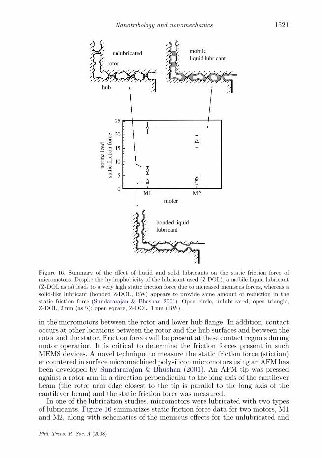
in the micromotors between the rotor and lower hub flange. In addition, contactoccurs at other locations between the rotor and the hub surfaces and between therotor and the stator. Friction forces will be present at these contact regions duringmotor operation. It is critical to determine the friction forces present in suchMEMS devices. A novel technique to measure the static friction force (stiction)encountered in surface micromachined polysilicon micromotors using an AFM hasbeen developed by Sundararajan & Bhushan (2001). An AFM tip was pressedagainst a rotor arm in a direction perpendicular to the long axis of the cantileverbeam (the rotor arm edge closest to the tip is parallel to the long axis of thecantilever beam) and the static friction force was measured.
In one of the lubrication studies, micromotors were lubricated with two typesof lubricants. Figure 16 summarizes static friction force data for two motors, M1and M2, along with schematics of the meniscus effects for the unlubricated and
Phil. Trans. R. Soc. A (2008)
B. Bhushan1522
lubricated surfaces. Capillary condensation of water vapour from the environ-ment results in the formation of meniscus bridges between contacting and near-contacting asperities of two surfaces in close proximity to each other as shown inthe figure. For unlubricated surfaces, more menisci are formed at higherhumidity resulting in higher friction force between the surfaces. The formation ofmeniscus bridges is supported by the fact that the static friction force forunlubricated motors increases at high humidity (Sundararajan & Bhushan 2001).Solid bridging may occur near the rotor–hub interface due to silica residues afterthe first etching process. In addition, the drying process after the final etch canresult in liquid bridging formed by the drying liquid due to meniscus force atthese areas (Mastrangelo & Hsu 1993; Maboudian & Howe 1997; Bhushan 1999b,2002, 2003). Therefore, the initial static friction force will be quite high asevidenced by the solid data points in figure 16. Once the first movement of therotor permanently breaks these solid and liquid bridges, the static friction forceof the motors will drop (as seen in figure 16) to a value dictated predominantlyby the adhesive energies of the rotor and hub surfaces, the real area of contactbetween these surfaces and meniscus forces due to water vapour in the air, atwhich point the effect of lubricant films can be observed. Lubrication with amobile layer, even a thin one, results in very high static friction forces due tomeniscus effects of the lubricant liquid itself at and near the contact regions. Itshould be noted that a motor submerged in a liquid lubricant would result in afully flooded lubrication regime. In this case, there is no meniscus contributionand only the viscous contribution to the friction forces would be relevant.However, submerging the device in a lubricant may not be a practical method. Asolid-like hydrophobic lubricant layer (such as bonded Z-DOL) results infavourable friction characteristics of the motor. The hydrophobic nature of thelubricant inhibits meniscus formation between the contact surfaces andmaintains low friction even at high humidity (Sundararajan & Bhushan 2002).This suggests that solid-like hydrophobic lubricants are ideal for lubrication ofMEMS while mobile lubricants result in increased values of static friction force.
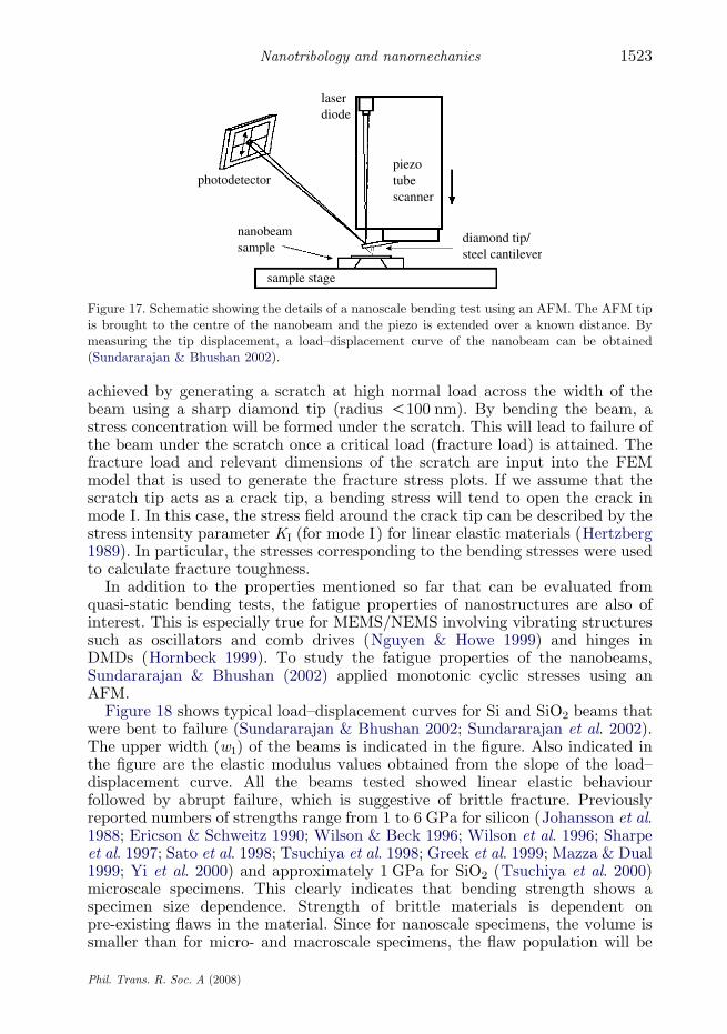
7. Bending tests of nanostructures using an AFM
Quasi-static bending tests of fixed nanobeam arrays have been carried out usingan AFM (Sundararajan & Bhushan 2002; Sundararajan et al. 2002). The waferwith nanobeam array with trapezoidal cross section is fixed onto a flat samplechuck using double-sided tape (Sundararajan & Bhushan 2002). For the bendingtest, the tip is brought over the nanobeam array with the help of the samplestage of the AFM (figure 17). Elastic modulus and bending strength (fracturestress) of the beams can be estimated from the load–displacement curves basedon the assumption that the beams are made of an isotropic material and followlinear elastic theory.
Fracture toughness is another important parameter for brittle materials suchas silicon. In the case of the nanobeam arrays, these are not best suited forfracture toughness measurements because they do not possess regions of uniformstress during bending. Sundararajan & Bhushan (2002) developed a method-ology. First, a crack of known geometry is introduced in the region of maximumtensile bending stress, i.e. on the top surface near the ends of the beam. This is
Phil. Trans. R. Soc. A (2008)
laserdiode
piezotubescanner
diamond tip/steel cantilever
photodetector
nanobeamsample
sample stage
Figure 17. Schematic showing the details of a nanoscale bending test using an AFM. The AFM tipis brought to the centre of the nanobeam and the piezo is extended over a known distance. Bymeasuring the tip displacement, a load–displacement curve of the nanobeam can be obtained(Sundararajan & Bhushan 2002).
1523Nanotribology and nanomechanics
achieved by generating a scratch at high normal load across the width of thebeam using a sharp diamond tip (radius !100 nm). By bending the beam, astress concentration will be formed under the scratch. This will lead to failure ofthe beam under the scratch once a critical load (fracture load) is attained. Thefracture load and relevant dimensions of the scratch are input into the FEMmodel that is used to generate the fracture stress plots. If we assume that thescratch tip acts as a crack tip, a bending stress will tend to open the crack inmode I. In this case, the stress field around the crack tip can be described by thestress intensity parameter KI (for mode I) for linear elastic materials (Hertzberg1989). In particular, the stresses corresponding to the bending stresses were usedto calculate fracture toughness.
In addition to the properties mentioned so far that can be evaluated fromquasi-static bending tests, the fatigue properties of nanostructures are also ofinterest. This is especially true for MEMS/NEMS involving vibrating structuressuch as oscillators and comb drives (Nguyen & Howe 1999) and hinges inDMDs (Hornbeck 1999). To study the fatigue properties of the nanobeams,Sundararajan & Bhushan (2002) applied monotonic cyclic stresses using anAFM.
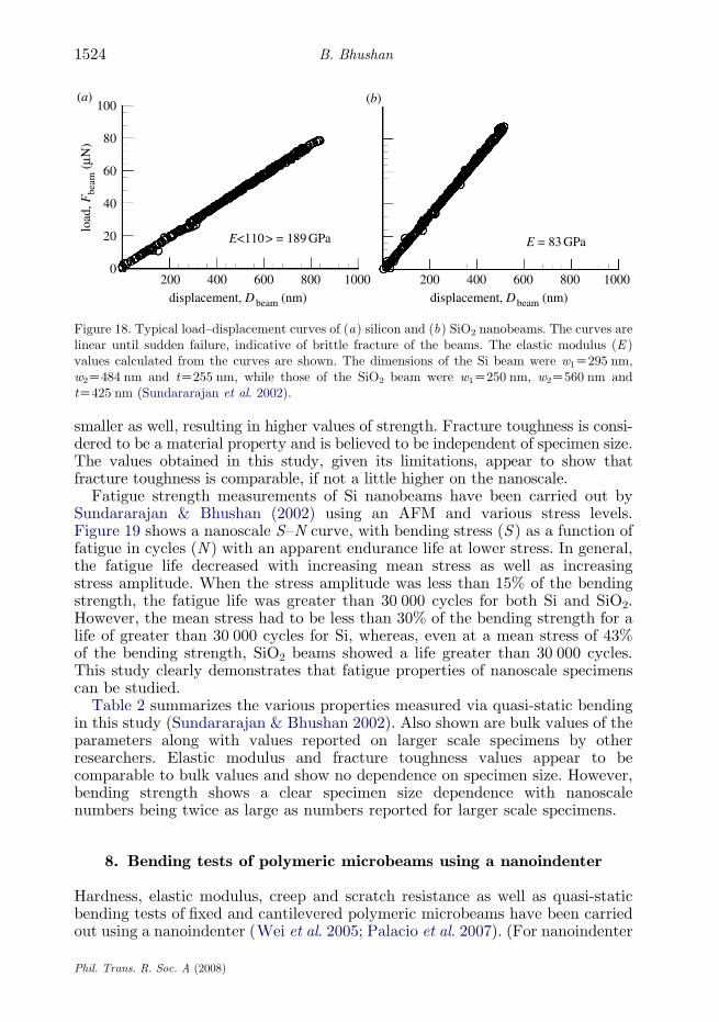
Figure 18 shows typical load–displacement curves for Si and SiO2 beams thatwere bent to failure (Sundararajan & Bhushan 2002; Sundararajan et al. 2002).The upper width (w1) of the beams is indicated in the figure. Also indicated inthe figure are the elastic modulus values obtained from the slope of the load–displacement curve. All the beams tested showed linear elastic behaviourfollowed by abrupt failure, which is suggestive of brittle fracture. Previouslyreported numbers of strengths range from 1 to 6 GPa for silicon (Johansson et al.1988; Ericson & Schweitz 1990; Wilson & Beck 1996; Wilson et al. 1996; Sharpeet al. 1997; Sato et al. 1998; Tsuchiya et al. 1998; Greek et al. 1999; Mazza & Dual1999; Yi et al. 2000) and approximately 1 GPa for SiO2 (Tsuchiya et al. 2000)microscale specimens. This clearly indicates that bending strength shows aspecimen size dependence. Strength of brittle materials is dependent onpre-existing flaws in the material. Since for nanoscale specimens, the volume issmaller than for micro- and macroscale specimens, the flaw population will be
Phil. Trans. R. Soc. A (2008)
100
80
60
20
40
0200 400 600 800 1000
E<110> = 189 GPa
load
, Fbe
am (
µN)
displacement, Dbeam (nm)200 400 600 800 1000
displacement, Dbeam (nm)
E = 83 GPa
(a) (b)
Figure 18. Typical load–displacement curves of (a) silicon and (b) SiO2 nanobeams. The curves arelinear until sudden failure, indicative of brittle fracture of the beams. The elastic modulus (E )values calculated from the curves are shown. The dimensions of the Si beam were w1Z295 nm,w2Z484 nm and tZ255 nm, while those of the SiO2 beam were w1Z250 nm, w2Z560 nm andtZ425 nm (Sundararajan et al. 2002).
B. Bhushan1524
smaller as well, resulting in higher values of strength. Fracture toughness is consi-dered to be a material property and is believed to be independent of specimen size.The values obtained in this study, given its limitations, appear to show thatfracture toughness is comparable, if not a little higher on the nanoscale.
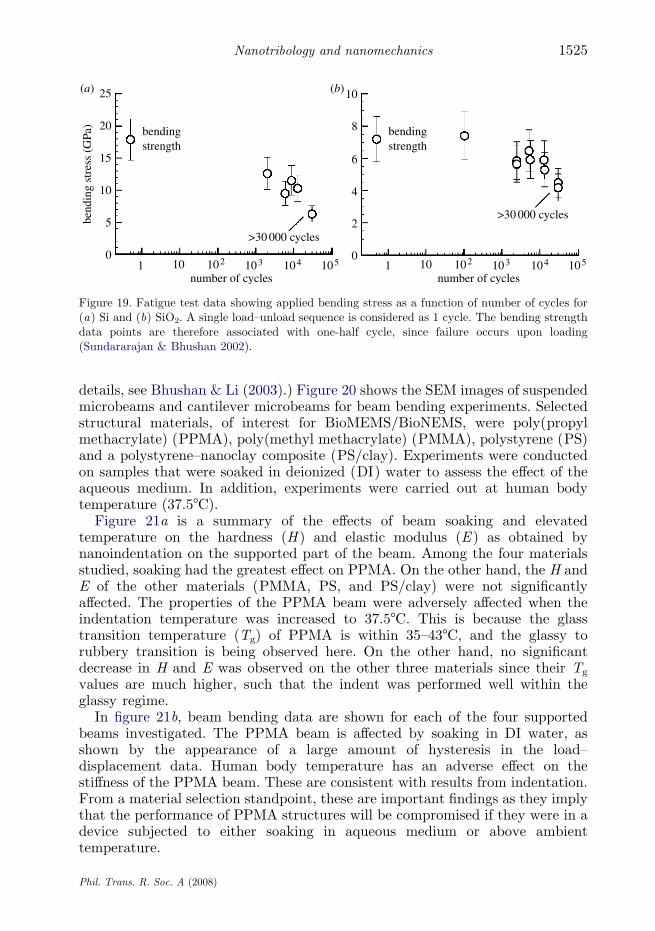
Fatigue strength measurements of Si nanobeams have been carried out bySundararajan & Bhushan (2002) using an AFM and various stress levels.Figure 19 shows a nanoscale S–N curve, with bending stress (S ) as a function offatigue in cycles (N ) with an apparent endurance life at lower stress. In general,the fatigue life decreased with increasing mean stress as well as increasingstress amplitude. When the stress amplitude was less than 15% of the bendingstrength, the fatigue life was greater than 30 000 cycles for both Si and SiO2.However, the mean stress had to be less than 30% of the bending strength for alife of greater than 30 000 cycles for Si, whereas, even at a mean stress of 43%of the bending strength, SiO2 beams showed a life greater than 30 000 cycles.This study clearly demonstrates that fatigue properties of nanoscale specimenscan be studied.
Table 2 summarizes the various properties measured via quasi-static bendingin this study (Sundararajan & Bhushan 2002). Also shown are bulk values of theparameters along with values reported on larger scale specimens by otherresearchers. Elastic modulus and fracture toughness values appear to becomparable to bulk values and show no dependence on specimen size. However,bending strength shows a clear specimen size dependence with nanoscalenumbers being twice as large as numbers reported for larger scale specimens.
8. Bending tests of polymeric microbeams using a nanoindenter
Hardness, elastic modulus, creep and scratch resistance as well as quasi-staticbending tests of fixed and cantilevered polymeric microbeams have been carriedout using a nanoindenter (Wei et al. 2005; Palacio et al. 2007). (For nanoindenter
Phil. Trans. R. Soc. A (2008)
25
20
15
10
5
0
bend
ing
stre
ss (
GPa
)10
8
6
4
2
0
bendingstrength
bendingstrength
>30 000 cycles
>30 000 cycles
1 10 102 103 104 105
number of cycles1 10 102 103 104 105
number of cycles
(a) (b)
Figure 19. Fatigue test data showing applied bending stress as a function of number of cycles for(a) Si and (b) SiO2. A single load–unload sequence is considered as 1 cycle. The bending strengthdata points are therefore associated with one-half cycle, since failure occurs upon loading(Sundararajan & Bhushan 2002).
1525Nanotribology and nanomechanics
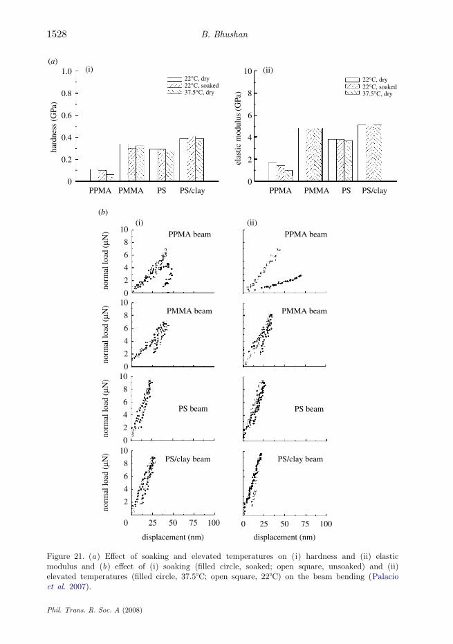
details, see Bhushan & Li (2003).) Figure 20 shows the SEM images of suspendedmicrobeams and cantilever microbeams for beam bending experiments. Selectedstructural materials, of interest for BioMEMS/BioNEMS, were poly(propylmethacrylate) (PPMA), poly(methyl methacrylate) (PMMA), polystyrene (PS)and a polystyrene–nanoclay composite (PS/clay). Experiments were conductedon samples that were soaked in deionized (DI) water to assess the effect of theaqueous medium. In addition, experiments were carried out at human bodytemperature (37.58C).
Figure 21a is a summary of the effects of beam soaking and elevatedtemperature on the hardness (H ) and elastic modulus (E ) as obtained bynanoindentation on the supported part of the beam. Among the four materialsstudied, soaking had the greatest effect on PPMA. On the other hand, the H andE of the other materials (PMMA, PS, and PS/clay) were not significantlyaffected. The properties of the PPMA beam were adversely affected when theindentation temperature was increased to 37.58C. This is because the glasstransition temperature (Tg) of PPMA is within 35–438C, and the glassy torubbery transition is being observed here. On the other hand, no significantdecrease in H and E was observed on the other three materials since their Tg
values are much higher, such that the indent was performed well within theglassy regime.
In figure 21b, beam bending data are shown for each of the four supportedbeams investigated. The PPMA beam is affected by soaking in DI water, asshown by the appearance of a large amount of hysteresis in the load–displacement data. Human body temperature has an adverse effect on thestiffness of the PPMA beam. These are consistent with results from indentation.From a material selection standpoint, these are important findings as they implythat the performance of PPMA structures will be compromised if they were in adevice subjected to either soaking in aqueous medium or above ambienttemperature.
Phil. Trans. R. Soc. A (2008)
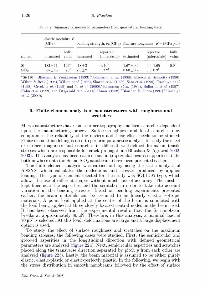
Table 2. Summary of measured parameters from quasi-static bending tests.
sample
elastic modulus, E(GPa) bending strength, sb (GPa) fracture toughness, KIC (MPa
ffiffiffiffiffim
p)
measuredbulkvalue measured
reported(microscale) estimated
reported(microscale)
bulkvalue
Si 182G11 169a 18G3 !10b 1.67G0.4 0.6–1.65c 0.9d
SiO2 85G13 73e 7.6G2 !2f 0.60G0.2 0.5–0.9f –
aSi(110), Bhushan & Venkatesan (1993).bJohansson et al. (1988), Ericson & Schweitz (1990),Wilson & Beck (1996), Wilson et al. (1996), Sharpe et al. (1997), Sato et al. (1998), Tsuchiya et al.(1998), Greek et al. (1999) and Yi et al. (2000).cJohansson et al. (1989), Ballarini et al. (1997),Kahn et al. (1999) and Fitzgerald et al. (2000).dAnon. (1988).eBhushan & Gupta (1997).fTsuchiyaet al. (2000).
B. Bhushan1526
9. Finite-element analysis of nanostructures with roughness andscratches
Micro/nanostructures have some surface topography and local scratches dependentupon the manufacturing process. Surface roughness and local scratches maycompromise the reliability of the devices and their effect needs to be studied.Finite-element modelling is used to perform parametric analysis to study the effectof surface roughness and scratches in different well-defined forms on tensilestresses which are responsible for crack propagation (Bhushan & Agrawal 2002,2003). The analysis has been carried out on trapezoidal beams supported at thebottom whose data (on Si and SiO2 nanobeams) have been presented earlier.
The finite-element analysis was carried out by using the static analysis ofANSYS, which calculates the deflections and stresses produced by appliedloading. The type of element selected for the study was SOLID95 type, whichallows the use of different shapes without much loss of accuracy. The mesh iskept finer near the asperities and the scratches in order to take into accountvariation in the bending stresses. Based on bending experiments presentedearlier, the beam materials can be assumed to be linearly elastic isotropicmaterials. A point load applied at the centre of the beam is simulated withthe load being applied at three closely located central nodes on the beam used.It has been observed from the experimental results that the Si nanobeambreaks at approximately 80 mN. Therefore, in this analysis, a nominal load of70 mN is selected. At this load, deformations are large and a large displacementoption is used.
To study the effect of surface roughness and scratches on the maximumbending stresses, the following cases were studied. First, the semicircular andgrooved asperities in the longitudinal direction with defined geometricalparameters are analysed (figure 22a). Next, semicircular asperities and scratchesplaced along the transverse direction separated by pitch p from each other areanalysed (figure 22b). Lastly, the beam material is assumed to be either purelyelastic, elastic-plastic or elastic-perfectly plastic. In the following, we begin withthe stress distribution in smooth nanobeams followed by the effect of surface
Phil. Trans. R. Soc. A (2008)
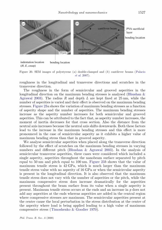
indentation location(H, E, creep)
bending location
bending location
50 µmcrossbeamsupport
cantilever beam PVA sacrificiallayer
(a) (b)
10 µm
Figure 20. SEM images of polystyrene (a) double-clamped and (b) cantilever beams (Palacioet al. 2007).
1527Nanotribology and nanomechanics
roughness in the longitudinal and transverse directions and scratches in thetransverse direction.
The roughness in the form of semicircular and grooved asperities in thelongitudinal direction on the maximum bending stresses is analysed (Bhushan &Agrawal 2003). The radius R and depth L are kept fixed at 25 nm, while thenumber of asperities is varied and their effect is observed on the maximum bendingstresses. Figure 23a shows the variation of maximum bending stresses as a functionof asperity shape and the number of asperities. The maximum bending stressesincrease as the asperity number increases for both semicircular and groovedasperities. This can be attributed to the fact that, as asperity number increases, themoment of inertia decreases for that cross section. Also the distance from theneutral axis increases because the neutral axis shifts downwards. Both these factorslead to the increase in the maximum bending stresses and this effect is morepronounced in the case of semicircular asperity as it exhibits a higher value ofmaximum bending stress than that in grooved asperity.
We analyse semicircular asperities when placed along the transverse directionfollowed by the effect of scratches on the maximum bending stresses in varyingnumbers and different pitch (Bhushan & Agrawal 2003). In the analysis ofsemicircular transverse asperities, three cases were considered which included asingle asperity, asperities throughout the nanobeam surface separated by pitchequal to 50 nm and pitch equal to 100 nm. Figure 23b shows that the value ofmaximum tensile stress is 42 GPa, which is much larger than the maximumtensile stress value with no asperity of 16 GPa or when the semicircular asperityis present in the longitudinal direction. It is also observed that the maximumtensile stress does not vary with the number of asperities or the pitch, while themaximum compressive stress does increase dramatically for the asperitiespresent throughout the beam surface from its value when a single asperity ispresent. Maximum tensile stress occurs at the ends and an increase in p does notadd any asperities at the ends whereas asperities are added in the central regionwhere compressive stresses are maximum. The semicircular asperities present atthe centre cause the local perturbation in the stress distribution at the centre ofthe asperity where load is being applied leading to a high value of maximumcompressive stress (Timoshenko & Goodier 1970).
Phil. Trans. R. Soc. A (2008)
1.0 (i) (ii)
0.8
0.6
0.4
0.2
0
10
8
6
4
2
0
hard
ness
(G
Pa)
22°C, dry 22°C, dry22°C, soaked 22°C, soaked37.5°C, dry 37.5°C, dry
elas
tic m
odul
us (
GPa
)PPMA beam
PMMA beam PMMA beam
PPMA beam
PMMAPPMA PS
PS beam PS beam
PS/clayPMMAPPMA PS PS/clay
PS/clay beam PS/clay beam
(i) (ii)10
10
10
10
8
8
8
8
6
6
6
6
4
4
4
4
2
2
2
2
0
0
0
0 025 2550 5075 75100 100
displacement (nm) displacement (nm)
(b)
(a)
norm
al lo
ad (
µN)
norm
al lo
ad (
µN)
norm
al lo
ad (
µN)
norm
al lo
ad (
µN)
Figure 21. (a ) Effect of soaking and elevated temperatures on (i) hardness and (ii) elasticmodulus and (b) effect of (i) soaking (filled circle, soaked; open square, unsoaked) and (ii)elevated temperatures (filled circle, 37.58C; open square, 228C) on the beam bending (Palacioet al. 2007).
B. Bhushan1528
Phil. Trans. R. Soc. A (2008)
1529Nanotribology and nanomechanics
In the study pertaining to scratches, the number of scratches is varied.Furthermore, the load is applied at the centre of the beam and at the centre of thescratch near the end as well for all the cases. In all of these cases, the pitch valuewas equal to 100 nm, and the L value was equal to 100 nm with the h value being20 nm. Figure 23c shows that the value of maximum tensile stress remains almostthe same with the number of scratches for both types of loading, i.e. when load isapplied at the centre of the beam and at the centre of the scratch near the end. Thisis because the maximum tensile stress occurs at the beam ends, no matter wherethe load gets applied. But the presence of scratch does increase the maximumtensile stress when compared with its value for a smooth nanobeam, although thenumber of scratches no longer matters because the maximum tensile stressoccurring at the nanobeam end is unaffected by the presence of more scratchesbeyond the first scratch in the direction towards the centre. The value of the tensilestress is much lower when the load is applied at the centre of the scratch and it canbe explained as follows. The negative bending moment at the end near the loadapplied decreases with load offset after two-thirds of the length of the beam(Shigley & Mitchell 1993). Since this negative bending moment is responsible fortensile stresses, their behaviour with the load offset is the same as the negativebending moment. Also the value of maximum compressive stress when load isapplied at the centre of the nanobeam remains almost the same as the centregeometry is unchanged due to the number of scratches and hence the maximumcompressive stress occurring below the load at the centre being the same. On theother hand, when the load is applied at the centre of the scratch we observe thatthe maximum compressive stress increases dramatically because the localperturbation in the stress distribution at the centre of the scratch where theload is being applied leads to a high value of maximum compressive stress(Timoshenko & Goodier 1970). It increases further with the number of scratchesand then levels off. This can be attributed to the fact that, when there is anotherscratch present close to the scratch near the end, the stress concentration is moreas the effect of local perturbation in the stress distribution is more significant.However, this effect is insignificant when more than two scratches are present.
Now we address the effect of pitch on the maximum compressive stress whenthe load is applied at the centre of the scratch near the end. When the pitch is upto a value of 200 nm, the maximum compressive stress increases with the numberof scratches as discussed earlier. On the other hand, when the pitch value goesbeyond 225 nm, this effect is reversed. This is because the presence of anotherscratch no longer affects the local perturbation in the stress distribution at thescratch near the end. Instead more scratches at a fair distance distribute themaximum compressive stress at the scratch near the end and the stress startsgoing down. Such observations of maximum bending stresses can help inidentifying the number of asperities and scratches allowed separated by anoptimum distance from each other.
10. Closure
In MEMS/NEMS, the length-scale and large surface-to-volume ratio of thedevices result in very high retarding forces such as adhesion and friction thatseriously undermine the performance and reliability of the devices. These
Phil. Trans. R. Soc. A (2008)
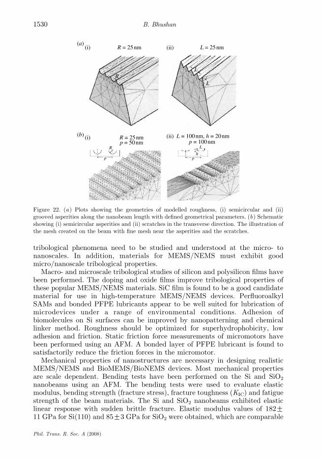
(i)
(i)
(ii)
(ii)
R = 25nm
R = 25nmp = 50nm p = 100nm
L = 25nm
L = 100nm, h = 20nm
R
p ph
L
(a)
(b)
RL
L
Figure 22. (a ) Plots showing the geometries of modelled roughness, (i) semicircular and (ii)grooved asperities along the nanobeam length with defined geometrical parameters. (b ) Schematicshowing (i) semicircular asperities and (ii) scratches in the transverse direction. The illustration ofthe mesh created on the beam with fine mesh near the asperities and the scratches.
B. Bhushan1530
tribological phenomena need to be studied and understood at the micro- tonanoscales. In addition, materials for MEMS/NEMS must exhibit goodmicro/nanoscale tribological properties.
Macro- and microscale tribological studies of silicon and polysilicon films havebeen performed. The doping and oxide films improve tribological properties ofthese popular MEMS/NEMS materials. SiC film is found to be a good candidatematerial for use in high-temperature MEMS/NEMS devices. PerfluoroalkylSAMs and bonded PFPE lubricants appear to be well suited for lubrication ofmicrodevices under a range of environmental conditions. Adhesion ofbiomolecules on Si surfaces can be improved by nanopatterning and chemicallinker method. Roughness should be optimized for superhydrophobicity, lowadhesion and friction. Static friction force measurements of micromotors havebeen performed using an AFM. A bonded layer of PFPE lubricant is found tosatisfactorily reduce the friction forces in the micromotor.
Mechanical properties of nanostructures are necessary in designing realisticMEMS/NEMS and BioMEMS/BioNEMS devices. Most mechanical propertiesare scale dependent. Bending tests have been performed on the Si and SiO2
nanobeams using an AFM. The bending tests were used to evaluate elasticmodulus, bending strength (fracture stress), fracture toughness (KIC) and fatiguestrength of the beam materials. The Si and SiO2 nanobeams exhibited elasticlinear response with sudden brittle fracture. Elastic modulus values of 182G11 GPa for Si(110) and 85G3 GPa for SiO2 were obtained, which are comparable
Phil. Trans. R. Soc. A (2008)
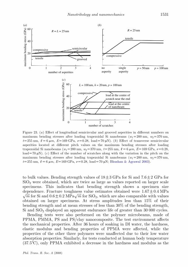
R = L = 25nm R = 25nm
p = 50nm
L = 100nm, h = 20nm, p = 100nm
p = 100nm
60
60
40
40
20
20
0
0 1 2 3 4
1 2 3 4number of asperities
number of scratches
max
imum
ben
ding
str
ess
(GPa
)
max
imum
ben
ding
str
ess
(GPa
)
compressive
compressive
compressive
semicircular
groovedtensile
tensile
tensile
noasperity
singleasperity
load at the centre ofscratch near the end
load at the centreof nanobeam
(a) (b)
(c)
Figure 23. (a) Effect of longitudinal semicircular and grooved asperities in different numbers onmaximum bending stresses after loading trapezoidal Si nanobeams (w1Z200 nm, w2Z370 nm,tZ255 nm, [Z6 mm, EZ169 GPa, nZ0.28, loadZ70 mN). (b) Effect of transverse semicircularasperities located at different pitch values on the maximum bending stresses after loadingtrapezoidal Si nanobeams (w1Z200 nm, w2Z370 nm, tZ255 nm, [Z6 mm, EZ169 GPa, nZ0.28,loadZ70 mN). (c) Effect of the number of scratches along with the variation in the pitch on themaximum bending stresses after loading trapezoidal Si nanobeams (w1Z200 nm, w2Z370 nm,tZ255 nm, [Z6 mm, EZ169 GPa, nZ0.28, loadZ70 mN; Bhushan & Agrawal 2003).
1531Nanotribology and nanomechanics
to bulk values. Bending strength values of 18G3 GPa for Si and 7.6G2 GPa forSiO2 were obtained, which are twice as large as values reported on larger scalespecimens. This indicates that bending strength shows a specimen sizedependence. Fracture toughness value estimates obtained were 1:67G0:4 MPaffiffiffiffiffim
pfor Si and 0:6G0:2 MPa
ffiffiffiffiffim
pfor SiO2, which are also comparable with values
obtained on larger specimens. At stress amplitudes less than 15% of theirbending strength and at mean stresses of less than 30% of the bending strength,Si and SiO2 displayed an apparent endurance life of greater than 30 000 cycles.
Bending tests were also performed on the polymer microbeams, made ofPPMA, PMMA, PS and PS/clay nanocomposite. The test environment affectsthe mechanical properties. After 36 hours of soaking in DI water, the hardness,elastic modulus and bending properties of PPMA were affected, while theproperties of the other three polymers were unaffected due to their low waterabsorption properties. Similarly, for tests conducted at human body temperature(37.58C), only PPMA exhibited a decrease in the hardness and modulus as the
Phil. Trans. R. Soc. A (2008)

B. Bhushan1532
other materials did not exhibit any change because this temperature is withinthe glass transition temperature range of the former but well below the Tg of theother polymers. Adding nanoclay filler improves bending strength.
The AFM and nanoindenters used in this study can be satisfactorily used toevaluate the micro/nanoscale tribological properties and mechanical propertiesof micro/nanoscale structures for use in MEMS/NEMS.
FEM simulations have been used to analyse the effect of type of surfaceroughness and scratches on stresses and deformation of nanostructures. We findthat roughness affects the maximum bending stresses. The maximum bendingstresses increase as the asperity number increases for both semicircular andgrooved asperities in longitudinal direction. When the semicircular asperity ispresent in the transverse direction, the maximum tensile stress is much largerthan the maximum tensile stress value with no asperity or when thesemicircular asperity is present in the longitudinal direction. This observationsuggests that the asperity in the transverse direction is more detrimental. Thepresence of scratches increases the maximum tensile stress. The maximumtensile stress remains almost the same with the number of scratches for twotypes of loading, i.e. when load is applied at the centre of the beam or at thecentre of the scratch near the end, although the value of the tensile stress ismuch lower when the load is applied at the centre of the scratch. This meansthat the load applied at the ends is less damaging. This analysis shows thatFEM simulations can be useful to designers to develop the most suitablegeometry for nanostructures.
References
Adamson, A. V. 1990 Physical chemistry of surfaces. New York, NY: Wiley.Anon. 1988 Properties of silicon. EMIS Datareviews Series, no. 4. London, UK: INSPEC,
Institution of Electrical Engineers.Ballarini, R., Mullen, R. L., Yin, Y., Kahn, H., Stemmer, S. & Heuer, A. H. 1997 The fracture
toughness of polysilicon microdevices: a first report. J. Mater. Res. 12, 915–922.Bhushan, B. 1996 Tribology and mechanics of magnetic storage devices, 2nd edn. New York, NY:
Springer.Bhushan, B. 1998 Tribology issues and opportunities in MEMS. Dordrecht, The Netherlands:
Kluwer Academic Publishers.Bhushan, B. 1999a Handbook of micro/nanotribology, 2nd edn. Boca Raton, FL: CRC Press.Bhushan, B. 1999b Principles and applications of tribology. New York, NY: Wiley.Bhushan, B. 1999c Chemical, mechanical and tribological characterization of ultra-thin and hard
amorphous carbon coatings as thin as 3.5 nm: recent developments. Diamond Relat. Mater. 8,1985–2015. (doi:10.1016/S0925-9635(99)00158-2)
Bhushan, B. 2001 Modern tribology handbook. Boca Raton, FL: CRC Press.Bhushan, B. 2002 Introduction to tribology. New York, NY: Wiley.Bhushan, B. 2003 Adhesion and stiction: mechanisms, measurement techniques, and methods for
reduction. J. Vac. Sci. Technol. B 21, 2262–2296. (doi:10.1116/1.1627336)Bhushan, B. 2005a Nanotribology and nanomechanics—an introduction. Heidelberg, Germany:
Springer.Bhushan, B. 2005b Nanotribology and nanomechanics. Wear 259, 1507–1531. (doi:10.1016/j.wear.
2005.01.010)Bhushan, B. 2007a Springer handbook of nanotechnology, 2nd edn. Heidelberg, Germany: Springer.Bhushan, B. 2007b Nanotribology and nanomechanics of MEMS/NEMS and BioMEMS/BioNEMS
materials and devices. Microelecron. Eng. 84, 387–412. (doi:10.1016/j.mee.2006.10.059)
Phil. Trans. R. Soc. A (2008)
1533Nanotribology and nanomechanics
Bhushan, B. & Agrawal, G. B. 2002 Stress analysis of nanostructures using a finite element
method. Nanotechnology 13, 515–523. (doi:10.1088/0957-4484/13/4/315)Bhushan, B. & Agrawal, G. B. 2003 Finite element analysis of nanostructures with roughness and
scratches. Ultramicroscopy 97, 495–507. (doi:10.1016/S0304-3991(03)00078-0)Bhushan, B. & Gupta, B. K. 1997 Handbook of tribology: materials, coatings and surface
treatments. Malabar, FL: Krieger. (Reprint edn.)Bhushan, B. & Jung, Y. C. 2006 Micro- and nanoscale characterization of hydrophobic and
hydrophilic leaf surfaces. Nanotechnology 17, 2758–2772. (doi:10.1088/0957-4484/17/11/008)Bhushan, B. & Jung, Y. C. 2007 Wetting study of patterned surfaces for superhydrophobicity.
Ultramicroscopy 107, 1033–1041. (doi:10.1016/j.ultramic.2007.05.002)Bhushan, B. & Koinkar, V. N. 1994 Tribological studies of silicon for magnetic recording
applications. J. Appl. Phys. 75, 5741–5746. (doi:10.1063/1.355601)Bhushan, B. & Li, X. 2003 Nanomechanical characterization of solid surfaces and thin films. Int.
Mater. Rev. 48, 125–164. (doi:10.1179/095066003225010227)Bhushan, B. & Liu, H. 2001 Nanotribological properties and mechanisms of alkylthiol and biphenyl
thiol self-assembled monolayers studied by AFM. Phys. Rev. B 63, 245412:1–11. (doi:10.1103/PhysRevB.63.245412)
Bhushan, B. & Venkatesan, S. 1993 Mechanical and tribological properties of silicon formicromechanical applications: a review. Adv. Inf. Storage Syst. 5, 211–239.
Bhushan, B., Israelachvili, J. N. & Landman, U. 1995a Nanotribology: friction, wear andlubrication at the atomic scale. Nature 374, 607–616. (doi:10.1038/374607a0)
Bhushan, B., Kulkarni, A. V., Koinkar, V. N., Boehm, M., Odoni, L., Martelet, C. & Belin, M.1995b Microtribological characterization of self-assembled and Langmuir–Blodgett monolayers
by atomic force and friction force microscopy. Langmuir 11, 3189–3198. (doi:10.1021/la00008a052)
Bhushan, B., Sundararajan, S., Li, X., Zorman, C. A. & Mehregany, M. 1998 Micro/nano-tribological studies of single-crystal silicon and polysilicon and SiC films for use in MEMS
devices. In Tribology issues and opportunities in MEMS (ed. B. Bhushan), pp. 407–430.Dordrecht, The Netherlands: Kluwer Academic Publishers.
Bhushan, B., Tokachichu, D. R., Keener, M. T. & Lee, S. C. 2005a Morphology and adhesion ofbiomolecules on silicon based surfaces. Acta Biomater. 1, 327–341. (doi:10.1016/j.actbio.2005.01.002)
Bhushan, B., Kasai, T., Kulik, G., Barbieri, L. & Hoffmann, P. 2005b AFM study of perfluorosilane
and alkylsilane self-assembled monolayers for anti-stiction in MEMS/NEMS. Ultramicroscopy105, 176–188. (doi:10.1016/j.ultramic.2005.06.034)
Bhushan, B., Tokachichu, D. R., Keener, M. T. & Lee, S. C. 2006a Nanoscale adhesion, frictionand wear studies of biomolecules on silicon based surfaces. Acta Biomater. 2, 39–49. (doi:10.1016/j.actbio.2005.08.010)
Bhushan, B., Cichomski, M., Hoque, E., DeRose, J. A., Hoffmann, P. & Mathieu, H. J. 2006b
Nanotribological characterization of perfluoroalkylphosphonate self-assembled monolayersdeposited on aluminum-coated silicon substrates. Microsyst. Technol. 12, 588–596. (doi:10.1007/s00542-006-0111-5)
Bhushan, B., Hansford, D. & Lee, K. K. 2006c Surface modification of silicon andpolydimethylsiloxane surfaces with vapor-phase-deposited ultrathin fluorosilane films for
biomedical nanodevices. J. Vac. Sci. Technol. A 24, 1197–1202. (doi:10.1116/1.2167077)Bhushan, B., Nosonovsky, M. & Jung, Y. C. 2007 Towards optimization of patterned
superhydrophobic surfaces. J. R. Soc. Interface 4, 643–648. (doi:10.1098/rsif.2006.0211)Burton, Z. & Bhushan, B. 2006 Surface characterization and adhesion and friction properties of
hydrophobic leaf surfaces. Ultramicroscopy 106, 709–716. (doi:10.1016/j.ultramic.2005.10.007)Cassie, A. & Baxter, S. 1944 Wetting of porous surfaces. Trans. Faraday Soc. 40, 546–551. (doi:10.
1039/tf9444000546)Core, T. A., Tsang, W. K. & Sherman, S. J. 1993 Fabrication technology for an integrated surface-
micromachined sensor. Solid State Technol. 36, 39–47.
Phil. Trans. R. Soc. A (2008)
B. Bhushan1534
Douglass, M. R. 1998 Lifetime estimates and unique failure mechanisms of the digital micromirror
devices (DMD). InProc. 36thAnnual Int.Reliability Physics Symp., pp. 9–16.NewYork,NY: IEEE.Douglass, M. R. 2003 DMD reliability: a MEMS success story, in reliability, testing, and
characterization of MEMS/MOEMS II. In Proc. of SPIE 4980, pp. 1–11. Bellingham, WA: SPIE.Ericson, F. & Schweitz, J. A. 1990 Micromechanical fracture strength of silicon. J. Appl. Phys. 68,
5840–5844. (doi:10.1063/1.346957)Extrand, C. W. 2004 Criteria for ultralyophobic surfaces. Langmuir 20, 5013–5018. (doi:10.1021/
la036481s)Fitzgerald, A. M., Dauskardt, R. H. & Kenny, T. W. 2000 Fracture toughness and crack growth
phenomena of plasma-etched single crystal silicon. Sens. Actuators A 83, 194–199. (doi:10.1016/
S0924-4247(99)00383-0)Greek, S., Ericson, F., Johansson, S., Furtsch, M. & Rump, A. 1999 Mechanical characterization of
thick polysilicon films: Young’s modulus and fracture strength evaluated with microstructures.J. Micromech. Microeng. 9, 245–251. (doi:10.1088/0960-1317/9/3/305)
Gupta, B. K. & Bhushan, B. 1994 Nanoindentation studies of ion implanted silicon. Surf. Coat.
Technol. 68–69, 564–570. (doi:10.1016/0257-8972(94)90218-6)Gupta, B. K., Chevallier, J. & Bhushan, B. 1993 Tribology of ion bombarded silicon for
micromechanical applications. ASME J. Tribol. 115, 392–399.Gupta, B. K., Bhushan, B. & Chevallier, J. 1994 Modification of tribological properties of silicon by
boron ion implantation. Tribol. Trans. 37, 601–607. (doi:10.1080/10402009408983335)Henck, S. A. 1997 Lubrication of digital micromirror devices. Tribol. Lett. 3, 239–247. (doi:10.
1023/A:1019129021492)Hertzberg, R. W. 1989 Deformation and fracture mechanics of engineering materials, pp. 277–278,
3rd edn. New York, NY: Wiley.Hornbeck, L. J. 1997 Low surface energy passivation layer for micromechanical devices. US Patent
no. 5,602,671, February 11.Hornbeck, L. J. 1999 A Digital Light Processinge update—status and future applications. In Proc.
Soc. Photo-Opt. Eng. 3634, Projection Displays V, pp. 158–170. Bellingham, WA: SPIE.Hornbeck, L. J. 2001 The DMDTM projection display chip: a MEMS-based technology. MRS Bull.
26, 325–328.Hornbeck, L. J. & Nelson, W. E. 1988 Bistable deformable mirror device. In OSA technical digest
series, vol. 8. Spatial light modulators and applications, pp. 107–110. New York, NY: IEEE.Israelachvili, J. N. 1992 Intermolecular and surface forces, 2nd edn. London, UK: Academic Press.Johansson, S., Schweitz, J. A., Tenerz, L. & Tiren, J. 1988 Fracture testing of silicon
microelements in-situ in a scanning electron microscope. J. Appl. Phys. 63, 4799–4803.(doi:10.1063/1.340471)
Johansson, S., Ericson, F. & Schweitz, J. A. 1989 Influence of surface-coatings on elasticity,residual-stresses, and fracture properties of silicon microelements. J. Appl. Phys. 65, 122–128.
(doi:10.1063/1.342585)Jung, Y. C. & Bhushan, B. 2006 Contact angle, adhesion and friction properties of micro- and
nanopatterned polymers for superhydrophobicity. Nanotechnology 17, 4970–4980. (doi:10.1088/0957-4484/17/19/033)
Jung, Y. C. & Bhushan, B. 2008 Wetting behavior during evaporation and condensation of water
microdroplets on superhydrophobic patterned surfaces. J. Microsc. 229, 127–140. (doi:10.1111/j.1365-2818.2007.01875.x)
Kahn, H., Ballarini, R., Mullen, R. L. & Heuer, A. H. 1999 Electrostatically actuated failure ofmicrofabricated polysilicon fracture mechanics specimens. Proc. R. Soc. A 455, 3807–3823.
(doi:10.1098/rspa.1999.0478)Kasai, T., Bhushan, B., Kulik, G., Barbieri, L. & Hoffmann, P. 2005 Nanotribological study of
perfluorosilane SAMs for anti-stiction and low wear. J. Vac. Sci. Technol. B 23, 995–1003.(doi:10.1116/1.1913674)
Kijlstra, J., Reihs, K. & Klami, A. 2002 Roughness and topology of ultra-hydrophobic surfaces.Colloids Surf. A: Physicochem. Eng. Asp. 206, 521–529. (doi:10.1016/S0927-7757(02)00089-4)
Phil. Trans. R. Soc. A (2008)
1535Nanotribology and nanomechanics
Koch, K., Dommisse, A. & Barthlott, W. 2006 Chemistry and crystal growth of plant wax tubules
of lotus (Nelumbo nucifera) and nasturtium (Tropaeolum majus) leaves on technical substrates.Cryst. Growth Des. 6, 2571–2578. (doi:10.1021/cg060035w)
Koinkar, V. N. & Bhushan, B. 1996a Micro/nanoscale studies of boundary layers of liquidlubricants for magnetic disks. J. Appl. Phys. 79, 8071–8075. (doi:10.1063/1.362361)
Koinkar, V. N. & Bhushan, B. 1996b Microtribological studies of unlubricated and lubricatedsurfaces using atomic force/friction force microscopy. J. Vac. Sci. Technol. A 14, 2378–2391.
(doi:10.1116/1.580026)Lafuma, A. & Quere, D. 2003 Superhydrophobic states. Nat. Mater. 2, 457–460. (doi:10.1038/
nmat924)Lee, S. C., Keener, M. T., Tokachichu, D. R., Bhushan, B., Barnes, P. D., Cipriany, B. R., Gao, M.
& Brillson, L. J. 2005a Preparation of a thin protein surface on thermally grown silicon dioxide.J. Vac. Sci. Technol. B 23, 1856–1865. (doi:10.1116/1.2006127)
Lee, K. K., Bhushan, B. & Hansford, D. 2005b Nanotribological characterization of
perfluoropolymer thin films for biomedical micro/nanoelectromechanical systems andapplications. J. Vac. Sci. Technol. A 23, 804–810. (doi:10.1116/1.1861939)
Li, X. & Bhushan, B. 1999 Micro/nanomechanical characterization of ceramic films formicrodevices. Thin Solid Films 340, 210–217. (doi:10.1016/S0040-6090(98)01153-5)
Li, X. & Bhushan, B. 2003 Fatigue studies of nanoscale structures for MEMS/NEMS applicationsusing nanoindentation techniques. Surf. Coat. Technol. 163–164, 521–526. (doi:10.1016/S0257-
8972(02)00662-X)Li, X., Bhushan, B., Takashima, K., Baek, C. W. & Kim, Y. K. 2003 Mechanical characterization
of micro/nanoscale structures for MEMS/NEMS applications using nanoindentationtechniques. Ultramicroscopy 97, 481–494. (doi:10.1016/S0304-3991(03)00077-9)
Liu, H. & Bhushan, B. 2002 Investigation of nanotribological properties of self-assembledmonolayers with alkyl and biphenyl spacer chains. Ultramicroscopy 91, 185–202. (doi:10.1016/S0304-3991(02)00099-2)
Liu, H. & Bhushan, B. 2003 Nanotribological characterization of molecularly-thick lubricant films
for applications to MEMS/NEMS by AFM. Ultramicroscopy 97, 321–340. (doi:10.1016/S0304-3991(03)00058-5)
Liu, H., Bhushan, B., Eck, W. & Stadler, V. 2001 Investigation of the adhesion, friction, and wearproperties of biphenyl thiol self-assembled monolayers by atomic force microscopy. J. Vac. Sci.Technol. A 19, 1234–1240. (doi:10.1116/1.1353538)
Maboudian, R. & Howe, R. T. 1997 Critical review: adhesion in surface micromechanical
structures. J. Vac. Sci. Technol. B 15, 1–20. (doi:10.1116/1.589247)Martin, J. R. & Zhao, Y. 1997 Micromachined device packaged to reduce stiction. US Patent no.
5,694,740, December 9.Mastrangelo, C. H. & Hsu, C. H. 1993 Mechanical stability and adhesion of microstructures under
capillary forces—part II: experiments. J. Microelectromech. Syst. 2, 44–55. (doi:10.1109/84.232594)
Mazza, E. & Dual, J. 1999 Mechanical behavior of a mm-sized single crystal silicon structure withsharp notches. J. Mech. Phys. Solids 47, 1795–1821. (doi:10.1016/S0022-5096(98)00112-4)
Mehregany, M., Zorman, C. A., Rajan, N. & Wu, C. H. 1998 Silicon carbide MEMS for harshenvironments. In Proc. IEEE, vol. 86, pp. 1594–1610. New York, NY: IEEE.
Namazu, T., Isono, Y. & Tanaka, T. 2000 Evaluation of size effect on mechanical properties of
single-crystal silicon by nanoscale bending test using AFM. J. Microelectromech. Syst. 9,450–459. (doi:10.1109/84.896765)
Neinhuis, C. & Barthlott, W. 1997 Characterization and distribution of water-repellent, self-cleaning plant surfaces. Ann. Bot. 79, 667–677. (doi:10.1006/anbo.1997.0400)
Nguyen, C. T. C. & Howe, R. T. 1999 An integrated CMOS micromechanical resonator high-Qoscillator. IEEE J. Solid St. Circ. 34, 440–455. (doi:10.1109/4.753677)
Nosonovsky, M. & Bhushan, B. 2005 Roughness optimization for biomimetic syperhydrophobicsurfaces. Microsyst. Technol. 11, 535–549. (doi:10.1007/s00542-005-0602-9)
Phil. Trans. R. Soc. A (2008)
B. Bhushan1536
Nosonovsky, M. & Bhushan, B. 2006 Stochastic model for metastable wetting of roughness-induced
superhydrophobic surfaces. Microsyst. Technol. 12, 273–281. (doi:10.1007/s00542-005-0067-x)
Nosonovsky, M. & Bhushan, B. 2007a Hierarchical roughness makes superhydrophobic states
stable. Microelectronic Eng. 84, 382–386. (doi:10.1016/j.mee.2006.10.054)
Nosonovsky, M. & Bhushan, B. 2007b Lotus effect: roughness-induced superhydrophobicity. In
Applied scanning probe methods, vol. 7 (eds B. Bhushan & H. Fuchs), pp. 1–40. Berlin,
Germany: Springer.
Palacio, M., Bhushan, B., Ferrell, N. & Hansford, D. 2007 Nanomechanical characterization of
polymer/silicon interfaces for biological micro-/nanomechanical system applications. Sens.
Actuators A 135, 637–650. (doi:10.1016/j.sna.2006.09.010)
Robbins, R. A. & Jacobs, S. J. 2001 Lubricant delivery for micromechanical devices. US Patent no.
6,300,294 B1, October 9.
Sato, K., Yoshioka, T., Anso, T., Shikida, M. & Kawabata, T. 1998 Tensile testing of silicon film
having different crystallographic orientations carried out on a silicon chip. Sens. Actuators A 70,
148–152. (doi:10.1016/S0924-4247(98)00125-3)
Sharpe Jr, W. N., Yuan, B. & Edwards, R. L. 1997 A new technique for measuring the mechanical
properties of thin films. J. Microelectromech. Syst. 6, 193–199. (doi:10.1109/84.623107)
Shigley, J. E. & Mitchell, L. D. 1993 Mechanical engineering design, 4th edn. New York, NY:
McGraw-Hill.
Shor, J. S., Goldstein, D. & Kurtz, A. D. 1993 Characterization of n-type b-SiC as a Piezoresistor.
IEEE Trans. Electron Devices 40, 1093–1099. (doi:10.1109/16.214734)
Sulouff, R. E. 1998MEMS opportunities in accelerometers and gyros and the microtribology problems
limiting commercialization. In Tribology issues and opportunities in MEMS (ed. B. Bhushan),
pp. 109–120. Dordrecht, The Netherlands: Kluwer Academic Publishers.
Sundararajan, S. & Bhushan, B. 1998 Micro/nanotribological studies of polysilicon and SiC films
for MEMS applications. Wear 217, 251–261. (doi:10.1016/S0043-1648(98)00169-0)
Sundararajan, S. & Bhushan, B. 2001 Static friction and surface roughness studies of surface
micromachined electrostatic micromotors using an atomic force/friction force microscope.
J. Vac. Sci. Technol. A 19, 1777–1785. (doi:10.1116/1.1353539)
Sundararajan, S. & Bhushan, B. 2002 Development of AFM-based techniques to measure
mechanical properties of nanoscale structures. Sens. Actuators A 101, 338–351. (doi:10.1016/
S0924-4247(02)00268-6)
Sundararajan, S., Bhushan, B., Namazu, T. & Isono, Y. 2002 Mechanical property measurements
of nanoscale structures using an atomic force microscope. Ultramicroscopy 91, 111–118. (doi:10.
1016/S0304-3991(02)00089-X)
Tambe, N. S. & Bhushan, B. 2005 Nanotribological characterization of self assembled monolayers
deposited on silicon and aluminum substrates. Nanotechnology 16, 1549–1559. (doi:10.1088/
0957-4484/16/9/024)
Tao, Z. & Bhushan, B. 2005a Bonding, degradation, and environmental effects on novel
perfluoropolyether lubrications. Wear 259, 1352–1361. (doi:10.1016/j.wear.2005.01.013)
Tao, Z. & Bhushan, B. 2005b Degradation mechanisms and environmental effects on
perfluoropolyether, self assembled monolayers, and diamondlike carbon films. Langmuir 21,
2391–2399. (doi:10.1021/la047853f)
Timoshenko, S. P. & Goodier, J. N. 1970 Theory of elasticity, 3rd edn. New York, NY:
McGraw-Hill.
Tsuchiya, T., Tabata, O., Sakata, J. & Taga, Y. 1998 Specimen size effect on tensile strength of
surface-micromachined polycrystalline silicon thin films. J. Microelectromech. Syst. 7, 106–113.
(doi:10.1109/84.661392)
Tsuchiya, T., Inoue, A. & Sakata, J. 2000 Tensile testing of insulating thin films: humidity effect on
tensile strength of SiO2 films. Sens. Actuators A 82, 286–290. (doi:10.1016/S0924-
4247(99)00363-5)
Phil. Trans. R. Soc. A (2008)
1537Nanotribology and nanomechanics
Wagner, P., Furstner, F., Barthlott, W. & Neinhuis, C. 2003 Quantitative assessment to thestructural basis of water repellency in natural and technical surfaces. J. Exp. Bot. 54,1295–1303. (doi:10.1093/jxb/erg127)
Wei, G., Bhushan, B., Ferrell, N. & Hansford, D. 2005 Microfabrication and nanomechanicalcharacterization of polymer MEMS for biological applications. J. Vac. Sci. Technol. A 23,811–819. (doi:10.1116/1.1861937)
Wenzel, R. N. 1936 Resistance of solid surfaces to wetting by water. Ind. Eng. Chem. 28, 988–994.(doi:10.1021/ie50320a024)
Wilson, C. J. & Beck, P. A. 1996 Fracture testing of bulk silicon microcantilever beams subjectedto a side load. J. Microelectromech. Syst. 5, 142–150. (doi:10.1109/84.536620)
Wilson, C. J., Ormeggi, A. & Narbutovskih, M. 1996 Fracture testing of silicon microcantileverbeams. J. Appl. Phys. 79, 2386–2393. (doi:10.1063/1.361102)
Yi, T., Li, L. & Kim, C. J. 2000 Microscale material testing of single crystalline silicon: processeffects on surface morphology and tensile strength. Sens. Actuators A 83, 172–178. (doi:10.1016/S0924-4247(00)00350-2)
Phil. Trans. R. Soc. A (2008)