Embed Size (px)
Citation preview
Review
Nanowire-Based Electrochemical BiosensorsAdam K. Wanekaya, Wilfred Chen, Nosang V. Myung,* Ashok Mulchandani*
Department of Chemical and Environmental Engineering and Center for Nanoscale Science and Engineering, University ofCalifornia, Riverside, CA 92521, USA*e-mail: [email protected]; [email protected]
Received: October 27, 2005Accepted: January 17, 2006
AbstractWe review recent advances in biosensors based on one-dimensional (1-D) nanostructure field-effect transistors (FET).Specifically, we address the fabrication, functionalization, assembly/alignment and sensing applications of FET basedon carbon nanotubes, silicon nanowires and conducting polymer nanowires. The advantages and disadvantages ofvarious fabrication, functionalization, and assembling procedures of these nanosensors are reviewed and discussed.We evaluate how they have been used for detection of various biological molecules and how such devices haveenabled the achievement of high sensitivity and selectivity with low detection limits. Finally, we conclude byhighlighting some of the challenges researchers face in the 1-D nanostructures research arena and also predict thedirection toward which future research in this area might be directed.
Keywords: Nanosensors, Biosensors, Field effect transistors (FETs), Carbon nanotubes, Conducting polymernanowires, Silicon nanowires, Metallic nanowires, One-dimensional nanostructures, Assembly, Magnetic alignment,Functionalization
DOI: 10.1002/elan.200503449
1. Introduction
One dimensional (1-D) nanostructures such as nanowires,nanotubes, nanobelts and nanosprings have become thefocus of intensive research due to their unique propertiesand their potential for fabrication into high density nano-scale devices including sensors, electronics, and optoelec-tronics. Further, 1-D nanostructures can be used for bothefficient transport of electrons and optical excitation, andthese two factors make them critical to the function andintegration of nanoscale devices. In fact, 1-D systems are thesmallest dimension structures that can be used for efficienttransport of electrons and are thus critical to the functionand integration of these nanoscale devices. Because of theirhigh surface-to-volume ratio and tunable electron transportproperties due to quantum confinement effect, their elec-trical properties are strongly influenced by minor perturba-tions (Fig. 1). Compared to 2-D thin films where binding tothe surface leads to depletion or accumulation of chargecarriers only on the surface of a planar device (Fig. 1A), thecharge accumulation or depletion in the 1-D nanostructuretakes place in the “bulk” of the structure (Fig. 1B) thusgiving rise to large changes in the electrical properties thatpotentially enables the detection of a single molecule. 1-Dnanostructures thus avoid the reduction in signal intensitiesthat are inherent in 2-D thin films as a result lateral currentshunting.This property of the 1-Dnanostructures provides asensing modality for label-free and direct electrical readoutwhen the nanostructure is used as a semiconducting channelof a chemiresistor or field-effect transistor [1]. Such label-
free and direct detection is particularly desirable for rapidand real-time monitoring of receptor – ligand interactionwith a receptor-modified nanostructure, particularly whenthe receptor is a biomolecule such as antibody, DNA, andproteins. This is critical for clinical diagnosis and biowarfareagents detection applications. Additionally, the sizes ofbiological macromolecules, such as proteins and nucleicacids are comparable to nanoscale building blocks. There-fore, any interaction between such molecules should inducesignificant changes in the electrical properties of 1-Dnanostructures. Further, 1-D nanostructures offer newcapabilities not available in larger scale devices (forexample, study of single molecule properties).This review summarizes recent advances in biosensors
based on 1-D nanostructures. Fabrication methods of 1-Dnanostructures are reviewed in Section 2, followed by theassembly and functionalization of the 1-D nanostructures inSections 3, 4 and 5. In Section 6, some significant applica-tions of 1-D nanostructures based sensors are discussed. InSection 7, the possible future directions of nanosensorsbased on 1-D nanostructures are suggested.
2. Fabrication of 1-D Nanostructures
A good method for generating 1-D nanostructures shouldenable simultaneous control of the dimensions, properties,andmorphology. In general, 1-D nanostructures are synthe-sized by promoting the crystallization of solid-state struc-tures along one direction by various mechanisms including:
533
Electroanalysis 18, 2006, No. 6, 533 – 550 C 2006 WILEY-VCH Verlag GmbH&Co. KGaA, Weinheim
– use of templates with 1-D morphologies to direct theformation of 1-D nanostructures
– use of the intrinsically anisotropic crystallographic struc-ture of a solid to achieve 1-D growth
– use of a liquid/solid interface to reduce the symmetry of aseed
– use of appropriate capping agents to kinetically controlthe growth rates of various facets of a seed.
The objective of this Section is to briefly describe methodsused to fabricate 1-D nanostructures such as silicon nano-wires (SiNWs), carbon nanotubes (CNTs), and conductingpolymer nanowires (CP NWs).
2.1. Carbon Nanotubes (CNTs)
Carbon nanotubes, first observed in 1991 [2], occur asmulti-walled nanotubes (MWNTs) and single-walled nanotubes(SWNTs) [3]. Primary methods for CNTs synthesis includearc-discharge [2, 4], laser ablation [5], gas-phase catalyticgrowth from carbon monoxide [6], and chemical vapordeposition (CVD) from hydrocarbons [7 – 9]. Becauseimpurities in the form of catalyst particles, amorphouscarbon, and nontubular fullerenes are also produced duringCNTs synthesis, subsequent purification steps are requiredto separate the tubes. The gas-phase processes tend toproduce nanotubes with fewer impurities and are moreamenable to large-scale processing.The arc-discharge technique generally involves the use of
two high purity graphite rods as the anode and cathode. Therods are brought together under a helium atmosphere and avoltage is applied until a stable arc is achieved. The exactprocess variables depend on the size of the graphite rods. Asthe anode is consumed, a constant gap between the anodeand cathode is maintained by adjusting the position of theanode. The material deposits on the cathode to form abuildup consisting of an outside shell of fusedmaterial and asofter fibrous core containing nanotubes and other carbonparticles. To create SWNTs, the electrodes are doped with asmall amount of catalyst particles [3, 4, 10 – 12].Initially used for the production of fullerenes, laser
ablation technique has, over the years, been improved toallow the production of SWNTs [5, 13, 14]. In this technique,
a graphite target held in a controlled atmosphere oven attemperatures near 1200 8C is vaporized by a laser and thevapors condensed over a water-cooled target. To produceSWNTs, the graphite target is doped with a catalyst [5].Both the arc-discharge and the laser ablation techniques
produce a limited volume of sample in relation to the size ofthe carbon source (the anode in arc-discharge and the targetin laser ablation) and require subsequent purification stepsto separate the tubes from undesirable byproducts. Theselimitations have motivated the development of gas-phasetechniques, such as chemical vapor deposition (CVD), inwhich nanotubes are formed by the decomposition of ahydrocarbon or carbon monoxide gas. The gas-phasetechniques are amenable to continuous processes since thecarbon source is continually replaced by flowing gas. Inaddition, the purity of the as-produced nanotubes can berelatively high, minimizing subsequent purification steps.Nikolaev et al. described the gas-phase growth of SWNTswith carbon monoxide as the carbon source [6]. Theyreported that the highest yields of SWNTs occurred at thehigh temperature and pressure (1200 8C, 10 atm). Smalleyandhis co-workers have refined the process to produce largequantities of SWNTswith increased purity. Other gas-phasetechniques utilize hydrocarbon gases as the carbon sourcefor production of both single and multi-walled carbonnanotubes [15 – 18].
2.2. Silicon Nanowires (SiNWs)
The first reported synthesis of SiNWs by thermal evapo-ration was by Yu et al., who sublimed a hot-pressed Sipowder targetmixedwithFe at 1200 8C in flowingAr gas at apressure of ca. 100 Torr [19]. Using this simplemethod, theyobtained SiNWs with a diameter of ca. 15 nm and lengthvarying from a few tens to hundreds of microns.The vapor– liquid – solid (VLS) method, involves the use
of liquid –metal solvents with low solubility for Si and otherelemental semiconductor materials. This method has beenvery successful in producing SiNWs in large quantities andat low temperatures [20]. The vapor– liquid – solid (VLS)method is the most successful in generating large quantitiesof nanowires with single crystalline structures. Originallydeveloped in 1964 for single crystals growth [21] the VLSmethod has since been used to synthesize various inorganicnanowires and nanorods [22 – 32]. In this VLS process, ametal, such as gold, that forms a low temperature eutecticphase with silicon is used as the catalyst for nanowiregrowth. A Si gas source (silane or silicon tetrachloride) ispassed over the metal catalyst, which is heated to atemperature greater than the eutectic temperature. The Sigas source decomposes on the surface of the catalyst, and Sidiffuses into the metal, forming an alloy. Upon reachingsupersaturation, SiNWs are precipitated and the liquid alloydrop remains on the nanowire as it grows in length. Thediameter of the SiNWs is controlled by the initial size of themetal catalyst [33] and, to some extent, the growthconditions [24, 34]. Porous alumina membranes have
Fig. 1. The major advantage of 1-D nanostructures (B) over 2-Dthin film (A). Binding to 1-D nanowire leads to depletion oraccumulation in the “bulk” of the nanowire as opposed to only thesurface in 2-D thin-film case.
534 A. K. Wanekaya et al.
Electroanalysis 18, 2006, No. 6, 533 – 550 www.electroanalysis.wiley-vch.de C 2006 WILEY-VCH Verlag GmbH&Co. KGaA, Weinheim
recently been used as an alternative to control nanowirediameter in the VLS process [35, 36]. Defect-free SiNWswith diameters in the range of 4 – 5 nmand lengths of severalmicrons were synthesized using a supercritical fluid solu-tion-phase approach wherein alkanethiol-coated Au nano-crystals (2.5 nm in diameter) were used as seeds to direct theone-dimensional crystallization of Si in a solvent heated andpressurized above its critical point [37]. The reactionpressure controlled the orientation of the nanowires.Another method that has been used to synthesize high
purity SiNWs is the laser ablation technique. In this methodhigh purity, crystalline nanowires were obtained in highyields [38] with diameters ranging from 3 to 43 nm andlengths extending up to a few hundred microns. Thediameters of the nanowires synthesized using laser ablationchange with the ambient gas used during the process [39].Thus, nanowires with different diameters have been synthe-sized in the presence of He, forming gas (95%Arþ 5%H2),and N2. Laser ablation has been combined with the VLSmethod with good results to synthesize semiconductornanowires [40]. In this process, laser ablation generatedthe nanometric catalyst clusters that then defined the size ofthe Si/Ge nanowires produced by the VLS growth. The useof targets of Si mixed with SiO2 enhanced the formation andgrowth of SiNWs obtained by laser ablation [41, 42]. SiO2
plays a more important role than the metal in the laserablation synthesis of SiNWs.Thermal methods have been applied to the synthesis of
SiNWs. For example, thermal evaporation of a mixture of SiandSiO2 yielded SiNWs that consisted of a polycrystalline Sicore with a high density of defects and a silicon oxide shell[43]. Highly oriented, long SiNWs have been obtained inlarge yields on flat silicon substrates by the thermalevaporation of SiO [44]. SiNWs have also been synthesizedby the thermal evaporation of SiO powders without anymetal catalyst [45]. These have been grown from particlesand the growth mechanism examined. The substrate tem-perature is crucial for controlling the diameter of thenanowires, as well as the morphologies resulting fromthermal evaporation of SiO powders mixed with 0 – 1% Fe[46]. Ultrafine SiNWs of diameters between 1 and 5 nm,sheathed with a SiO2 outer layer of 10 – 20 nm, weresynthesized by oxide-assisted growth via the disproportio-nation of thermally evaporated SiO using a zeolite template[47]. The zeolite restricted the growth of the nanowireslaterally and supplied the oxide to form the outer sheath.
2.3. Conducting Polymer Nanowires (CP NWs)
Among the methods that have been used to fabricateconducting polymers on the nanometer scale are electro-chemical dip-pen lithography, mechanical stretching [48],electrospinning [49, 50] and template-directed electrochem-ical synthesis [51].Dip-pen nanolithography (DPN) is a scanning probe
nanopatterning technique in which an AFM tip is used todeliver molecules to a surface via a solvent meniscus which
naturally forms in the ambient atmosphere. Doped polyani-line and polypyrrole lines down to 310 nm and 290 nmwidths, respectively, were formed using ionically chargedconducting polymers as the “ink” for writing on oppositelycharged substrates. Electrostatic interactions between thewater-soluble inkmaterials and charged substrates provideda significant driving force for the generation of stable DPNpatterns on the silicon substrates [52]. Similarly, writing ofpoly 3,4-ethylenedioxythiophene down to 30 nm by poly-merization of 3,4-ethylenedioxythiophene at the AFM tip/substrate was achieved [53].In the mechanical stretching procedure, conducting
polymer nanowires are fabricated by electrochemical poly-merization of the corresponding monomer onto a sharpscanning tunneling microscope (STM) tip that is held at asmall distance (between 20 – 100 nm) from an electrodefollowed by the reduction of the diameter of the depositedpolymer by stretching by moving the STM tip. Highlyconductive polyaniline wire with diameter of about 20 nmhas been reported using this method [48].Conducting polymers as nanofibers have also been
fabricated by electrospinning. This method uses a micro-fabricated scanned tip as an electrospinning source. The tipis dipped in a polymer solution to gather a droplet as asource material. A voltage applied to the tip causes theformation of a Taylor cone, and at sufficiently high voltages,a polymer jet is extracted from the droplet. By moving thesource relative to a surface, acting as a counter-electrode,oriented nanofibers can be deposited and integrated withmicrofabricated surface structures. In addition to the uni-form fiber deposition, the scanning tip electrospinningsource can produce self-assembled composite fibers ofmicro-and nanoparticles aligned in a polymeric fiber [54 –56].Like other one-dimensional nanostructures, 1-D conduct-
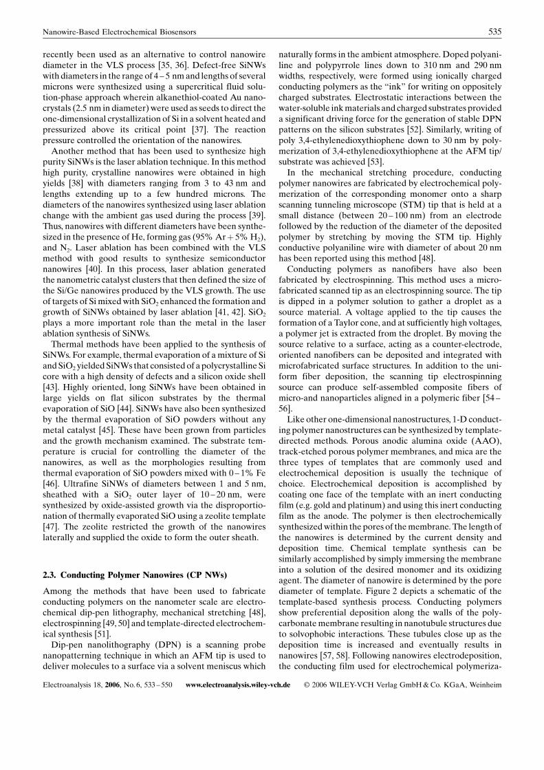
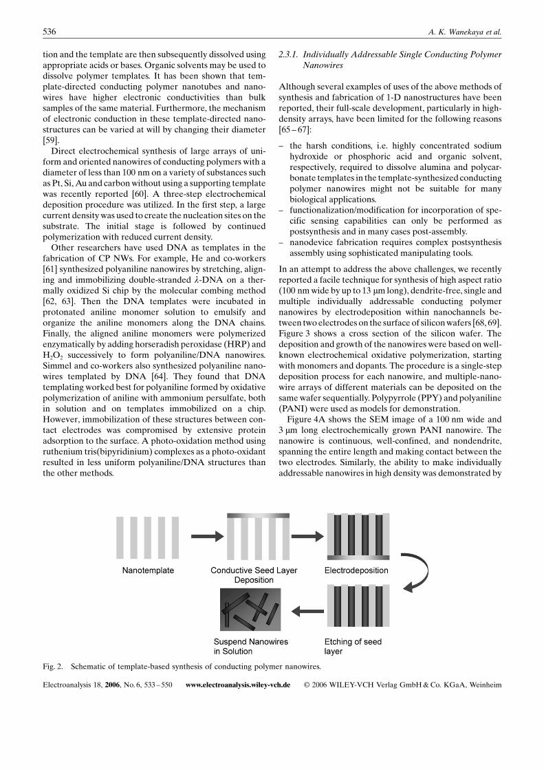
ing polymer nanostructures can be synthesized by template-directed methods. Porous anodic alumina oxide (AAO),track-etched porous polymer membranes, and mica are thethree types of templates that are commonly used andelectrochemical deposition is usually the technique ofchoice. Electrochemical deposition is accomplished bycoating one face of the template with an inert conductingfilm (e.g. gold and platinum) and using this inert conductingfilm as the anode. The polymer is then electrochemicallysynthesizedwithin the pores of themembrane. The length ofthe nanowires is determined by the current density anddeposition time. Chemical template synthesis can besimilarly accomplished by simply immersing the membraneinto a solution of the desired monomer and its oxidizingagent. The diameter of nanowire is determined by the porediameter of template. Figure 2 depicts a schematic of thetemplate-based synthesis process. Conducting polymersshow preferential deposition along the walls of the poly-carbonatemembrane resulting in nanotubule structures dueto solvophobic interactions. These tubules close up as thedeposition time is increased and eventually results innanowires [57, 58]. Following nanowires electrodeposition,the conducting film used for electrochemical polymeriza-
535Nanowire-Based Electrochemical Biosensors
Electroanalysis 18, 2006, No. 6, 533 – 550 www.electroanalysis.wiley-vch.de C 2006 WILEY-VCH Verlag GmbH&Co. KGaA, Weinheim
tion and the template are then subsequently dissolved usingappropriate acids or bases. Organic solvents may be used todissolve polymer templates. It has been shown that tem-plate-directed conducting polymer nanotubes and nano-wires have higher electronic conductivities than bulksamples of the same material. Furthermore, the mechanismof electronic conduction in these template-directed nano-structures can be varied at will by changing their diameter[59].Direct electrochemical synthesis of large arrays of uni-
form and oriented nanowires of conducting polymers with adiameter of less than 100 nm on a variety of substances suchas Pt, Si, Au and carbonwithout using a supporting templatewas recently reported [60]. A three-step electrochemicaldeposition procedure was utilized. In the first step, a largecurrent densitywas used to create the nucleation sites on thesubstrate. The initial stage is followed by continuedpolymerization with reduced current density.Other researchers have used DNA as templates in the
fabrication of CP NWs. For example, He and co-workers[61] synthesized polyaniline nanowires by stretching, align-ing and immobilizing double-stranded l-DNA on a ther-mally oxidized Si chip by the molecular combing method[62, 63]. Then the DNA templates were incubated inprotonated aniline monomer solution to emulsify andorganize the aniline monomers along the DNA chains.Finally, the aligned aniline monomers were polymerizedenzymatically by adding horseradish peroxidase (HRP) andH2O2 successively to form polyaniline/DNA nanowires.Simmel and co-workers also synthesized polyaniline nano-wires templated by DNA [64]. They found that DNAtemplating worked best for polyaniline formed by oxidativepolymerization of aniline with ammonium persulfate, bothin solution and on templates immobilized on a chip.However, immobilization of these structures between con-tact electrodes was compromised by extensive proteinadsorption to the surface. A photo-oxidation method usingruthenium tris(bipyridinium) complexes as a photo-oxidantresulted in less uniform polyaniline/DNA structures thanthe other methods.
2.3.1. Individually Addressable Single Conducting PolymerNanowires
Although several examples of uses of the above methods ofsynthesis and fabrication of 1-D nanostructures have beenreported, their full-scale development, particularly in high-density arrays, have been limited for the following reasons[65 – 67]:
– the harsh conditions, i.e. highly concentrated sodiumhydroxide or phosphoric acid and organic solvent,respectively, required to dissolve alumina and polycar-bonate templates in the template-synthesized conductingpolymer nanowires might not be suitable for manybiological applications.
– functionalization/modification for incorporation of spe-cific sensing capabilities can only be performed aspostsynthesis and in many cases post-assembly.
– nanodevice fabrication requires complex postsynthesisassembly using sophisticated manipulating tools.
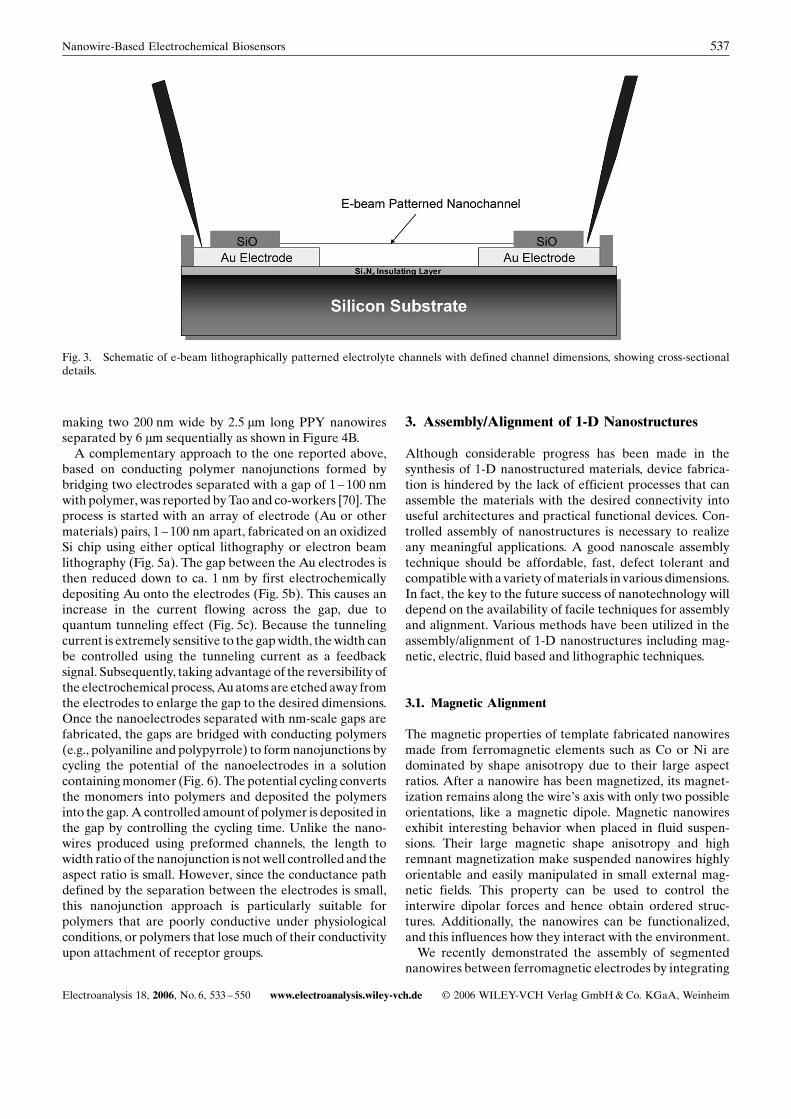
In an attempt to address the above challenges, we recentlyreported a facile technique for synthesis of high aspect ratio(100 nmwide by up to 13 mm long), dendrite-free, single andmultiple individually addressable conducting polymernanowires by electrodeposition within nanochannels be-tween twoelectrodes on the surface of siliconwafers [68, 69].Figure 3 shows a cross section of the silicon wafer. Thedeposition and growth of the nanowires were based on well-known electrochemical oxidative polymerization, startingwith monomers and dopants. The procedure is a single-stepdeposition process for each nanowire, and multiple-nano-wire arrays of different materials can be deposited on thesamewafer sequentially. Polypyrrole (PPY) and polyaniline(PANI) were used as models for demonstration.Figure 4A shows the SEM image of a 100 nm wide and
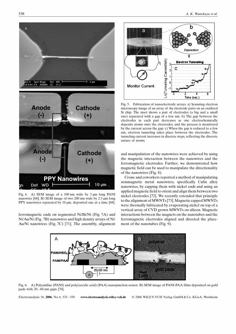
3 mm long electrochemically grown PANI nanowire. Thenanowire is continuous, well-confined, and nondendrite,spanning the entire length and making contact between thetwo electrodes. Similarly, the ability to make individuallyaddressable nanowires in high density was demonstrated by
Fig. 2. Schematic of template-based synthesis of conducting polymer nanowires.
536 A. K. Wanekaya et al.
Electroanalysis 18, 2006, No. 6, 533 – 550 www.electroanalysis.wiley-vch.de C 2006 WILEY-VCH Verlag GmbH&Co. KGaA, Weinheim
making two 200 nm wide by 2.5 mm long PPY nanowiresseparated by 6 mm sequentially as shown in Figure 4B.A complementary approach to the one reported above,
based on conducting polymer nanojunctions formed bybridging two electrodes separated with a gap of 1 – 100 nmwith polymer, was reported by Tao and co-workers [70]. Theprocess is started with an array of electrode (Au or othermaterials) pairs, 1 – 100 nm apart, fabricated on an oxidizedSi chip using either optical lithography or electron beamlithography (Fig. 5a). The gap between the Au electrodes isthen reduced down to ca. 1 nm by first electrochemicallydepositing Au onto the electrodes (Fig. 5b). This causes anincrease in the current flowing across the gap, due toquantum tunneling effect (Fig. 5c). Because the tunnelingcurrent is extremely sensitive to the gapwidth, thewidth canbe controlled using the tunneling current as a feedbacksignal. Subsequently, taking advantage of the reversibility ofthe electrochemical process,Auatoms are etched away fromthe electrodes to enlarge the gap to the desired dimensions.Once the nanoelectrodes separated with nm-scale gaps arefabricated, the gaps are bridged with conducting polymers(e.g., polyaniline and polypyrrole) to form nanojunctions bycycling the potential of the nanoelectrodes in a solutioncontainingmonomer (Fig. 6). The potential cycling convertsthe monomers into polymers and deposited the polymersinto the gap.A controlled amount of polymer is deposited inthe gap by controlling the cycling time. Unlike the nano-wires produced using preformed channels, the length towidth ratio of the nanojunction is notwell controlled and theaspect ratio is small. However, since the conductance pathdefined by the separation between the electrodes is small,this nanojunction approach is particularly suitable forpolymers that are poorly conductive under physiologicalconditions, or polymers that lose much of their conductivityupon attachment of receptor groups.
3. Assembly/Alignment of 1-D Nanostructures
Although considerable progress has been made in thesynthesis of 1-D nanostructured materials, device fabrica-tion is hindered by the lack of efficient processes that canassemble the materials with the desired connectivity intouseful architectures and practical functional devices. Con-trolled assembly of nanostructures is necessary to realizeany meaningful applications. A good nanoscale assemblytechnique should be affordable, fast, defect tolerant andcompatiblewith a variety ofmaterials in various dimensions.In fact, the key to the future success of nanotechnology willdepend on the availability of facile techniques for assemblyand alignment. Various methods have been utilized in theassembly/alignment of 1-D nanostructures including mag-netic, electric, fluid based and lithographic techniques.
3.1. Magnetic Alignment
The magnetic properties of template fabricated nanowiresmade from ferromagnetic elements such as Co or Ni aredominated by shape anisotropy due to their large aspectratios. After a nanowire has been magnetized, its magnet-ization remains along the wireNs axis with only two possibleorientations, like a magnetic dipole. Magnetic nanowiresexhibit interesting behavior when placed in fluid suspen-sions. Their large magnetic shape anisotropy and highremnant magnetization make suspended nanowires highlyorientable and easily manipulated in small external mag-netic fields. This property can be used to control theinterwire dipolar forces and hence obtain ordered struc-tures. Additionally, the nanowires can be functionalized,and this influences how they interact with the environment.We recently demonstrated the assembly of segmented
nanowires between ferromagnetic electrodes by integrating
Fig. 3. Schematic of e-beam lithographically patterned electrolyte channels with defined channel dimensions, showing cross-sectionaldetails.
537Nanowire-Based Electrochemical Biosensors
Electroanalysis 18, 2006, No. 6, 533 – 550 www.electroanalysis.wiley-vch.de C 2006 WILEY-VCH Verlag GmbH&Co. KGaA, Weinheim
ferromagnetic ends on segmented Ni/Bi/Ni (Fig. 7A) andNi/Au/Ni (Fig. 7B) nanowires and high density arrays of Ni/Au/Ni nanowires (Fig. 7C) [71]. The assembly, alignment
and manipulation of the nanowires were achieved by usingthe magnetic interaction between the nanowires and theferromagnetic electrodes. Further, we demonstrated howmagnetic field can be used to manipulate the directionalityof the nanowires (Fig. 8).Crone and coworkers reported a method of manipulating
nonmagnetic metal nanowires, specifically CuSn alloynanowires, by capping them with nickel ends and using anappliedmagnetic field to orient and align thembetween twonickel electrodes [72]. We recently extended that principleto the alignment ofMWNTs [73].Magnetic cappedMWNTswere thermally fabricated by evaporating nickel on top of avertical array of CVD grown MWNTs on silicon. Magneticinteractions between the magnets on the nanotubes and theferromagnetic electrodes aligned and directed the place-ment of the nanotubes (Fig. 9).
Fig. 4. A) SEM image of a 100 nm wide by 3 mm long PANInanowire [68]. B) SEM image of two 200 nm wide by 2.5 mm longPPY nanowires separated by 10 mm, deposited one at a time [68].
Fig. 5. Fabrication of nanoelectrode arrays. a) Scanning electronmicroscopy image of an array of Au electrode pairs on an oxidizedSi chip. The inset shows a pair of electrodes (a big and a smallone) separated with a gap of a few nm. b) The gap between theelectrodes in each pair decreases as one electrochemicallydeposits atoms onto the electrodes, and the process is monitoredby the current across the gap. c) When the gap is reduced to a fewnm, electron tunneling takes place between the electrodes. Thetunneling current increases in discrete steps, reflecting the discretenature of atoms.
Fig. 6. A) Polyaniline (PANI) and poly(acrylic acid) (PAA) nanojunction sensor. B) SEM image of PANI-PAA films deposited on goldpads with 20 – 60 nm gaps [70].
538 A. K. Wanekaya et al.
Electroanalysis 18, 2006, No. 6, 533 – 550 www.electroanalysis.wiley-vch.de C 2006 WILEY-VCH Verlag GmbH&Co. KGaA, Weinheim
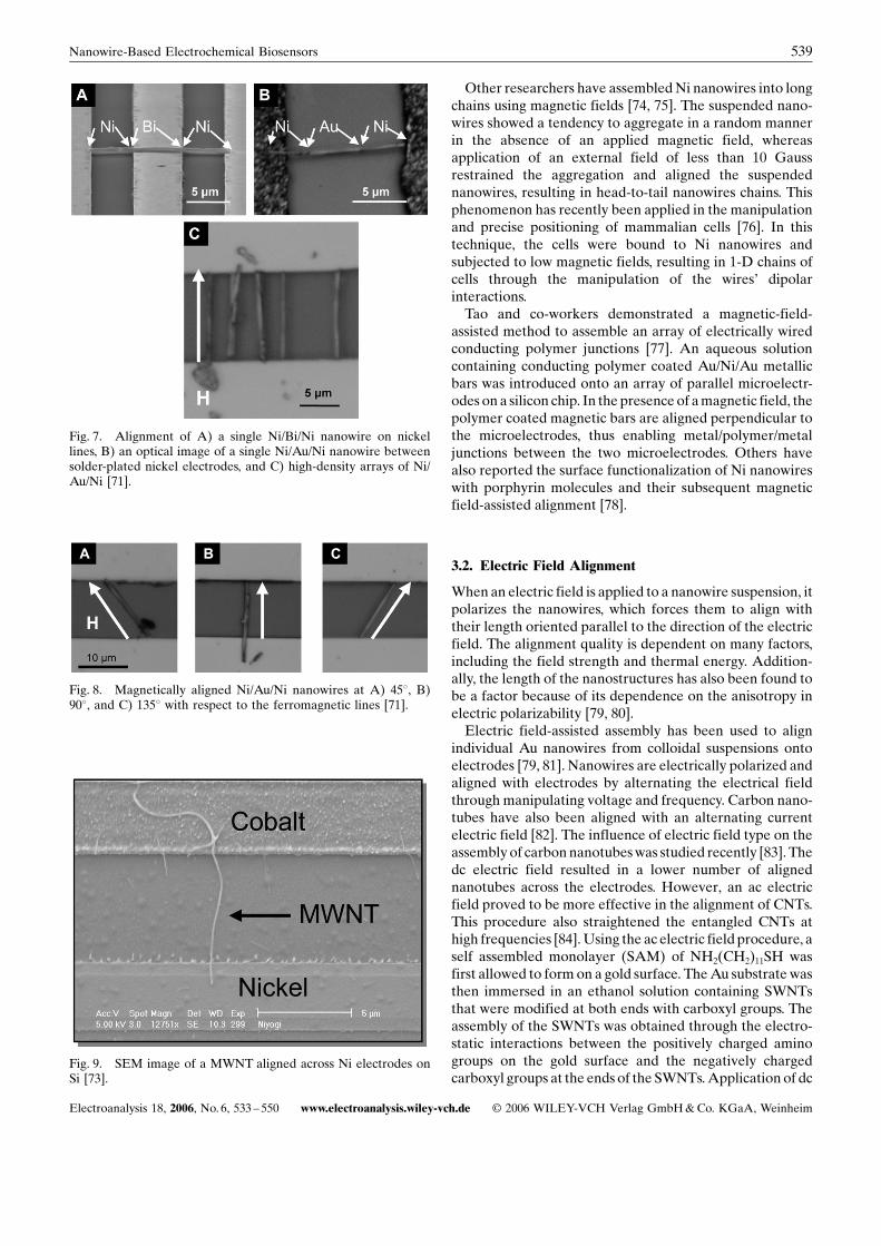
Other researchers have assembledNi nanowires into longchains using magnetic fields [74, 75]. The suspended nano-wires showed a tendency to aggregate in a random mannerin the absence of an applied magnetic field, whereasapplication of an external field of less than 10 Gaussrestrained the aggregation and aligned the suspendednanowires, resulting in head-to-tail nanowires chains. Thisphenomenon has recently been applied in the manipulationand precise positioning of mammalian cells [76]. In thistechnique, the cells were bound to Ni nanowires andsubjected to low magnetic fields, resulting in 1-D chains ofcells through the manipulation of the wiresN dipolarinteractions.Tao and co-workers demonstrated a magnetic-field-
assisted method to assemble an array of electrically wiredconducting polymer junctions [77]. An aqueous solutioncontaining conducting polymer coated Au/Ni/Au metallicbars was introduced onto an array of parallel microelectr-odes on a silicon chip. In the presence of amagnetic field, thepolymer coated magnetic bars are aligned perpendicular tothe microelectrodes, thus enabling metal/polymer/metaljunctions between the two microelectrodes. Others havealso reported the surface functionalization of Ni nanowireswith porphyrin molecules and their subsequent magneticfield-assisted alignment [78].
3.2. Electric Field Alignment
When an electric field is applied to a nanowire suspension, itpolarizes the nanowires, which forces them to align withtheir length oriented parallel to the direction of the electricfield. The alignment quality is dependent on many factors,including the field strength and thermal energy. Addition-ally, the length of the nanostructures has also been found tobe a factor because of its dependence on the anisotropy inelectric polarizability [79, 80].Electric field-assisted assembly has been used to align
individual Au nanowires from colloidal suspensions ontoelectrodes [79, 81]. Nanowires are electrically polarized andaligned with electrodes by alternating the electrical fieldthrough manipulating voltage and frequency. Carbon nano-tubes have also been aligned with an alternating currentelectric field [82]. The influence of electric field type on theassembly of carbonnanotubeswas studied recently [83]. Thedc electric field resulted in a lower number of alignednanotubes across the electrodes. However, an ac electricfield proved to be more effective in the alignment of CNTs.This procedure also straightened the entangled CNTs athigh frequencies [84].Using the ac electric field procedure, aself assembled monolayer (SAM) of NH2(CH2)11SH wasfirst allowed to formon a gold surface. TheAu substrate wasthen immersed in an ethanol solution containing SWNTsthat were modified at both ends with carboxyl groups. Theassembly of the SWNTs was obtained through the electro-static interactions between the positively charged aminogroups on the gold surface and the negatively chargedcarboxyl groups at the ends of the SWNTs.Application of dc
Fig. 7. Alignment of A) a single Ni/Bi/Ni nanowire on nickellines, B) an optical image of a single Ni/Au/Ni nanowire betweensolder-plated nickel electrodes, and C) high-density arrays of Ni/Au/Ni [71].
Fig. 8. Magnetically aligned Ni/Au/Ni nanowires at A) 458, B)908, and C) 1358 with respect to the ferromagnetic lines [71].
Fig. 9. SEM image of a MWNT aligned across Ni electrodes onSi [73].
539Nanowire-Based Electrochemical Biosensors
Electroanalysis 18, 2006, No. 6, 533 – 550 www.electroanalysis.wiley-vch.de C 2006 WILEY-VCH Verlag GmbH&Co. KGaA, Weinheim
electric field on the two gold substrate electrodes inducedthe alignment of SWNTs along the electric field. Siliconnanowires (SiNWs) have also been aligned by the applica-tion of an electric field [85].
3.3. Lithography
Heath and coworkers demonstrated the fabrication ofmetaland semiconductor nanowires of controllable dimensionsand ultrahigh density using lithographic techniques bytransferring prefabricated nanowires from templates toother surfaces [86]. However, it is still difficult to apply thisscheme beyond the fabrication of grids of identical metal orsilicon nanowires.
3.4. Langmuir – Blodgett Techniques
The Langmuir –Blodgett (LB) technique has been exten-sively used in the preparation of monolayers for molecularelectronics and more recently to create nanocrystal mono-layers with tunable properties [87]. The application of LBtechniques has been extended to the assembly of 1-Dnanostructures with large aspect ratios [88] and assembly ofSiNWs [89] and silver nanowires [90] have been demon-strated. The procedure starts with dispersing the nanowiresuspensions on the water surface of a Langmuir –Blodgetttrough using surfactants. The interaction between thesurfactants and the nanowires causes the nanowires to floaton the water surface and to align themselves parallel to thetrough barriers, forming a closely packed monolayer whichthen can be transferred to planar substrates. LB is thus thebest method for aligning 1-D nanostructures with a largeaspect ratio over a wide area. However, difficulties inproviding electrical contacts to individual nanowires and thelack of geometric versatility are challenges that need to beaddressed.
3.5. Biomolecule Mediated Self-Assembly
Braun and his co-worker reported the DNA mediated selfassembly of FETs based on CNTs [91]. In this approach, aSWNTwas localized at a desired address on aDNA scaffoldmolecule, using homologous recombination by the RecAprotein from E. Coli. DNA metallization led to theformation of wires that contacted the SWNT. Similarly,the ability of peptides to assemble SWNTs has also beendemonstrated [92, 93].
4. Functionalization of 1-D Nanostructures
Functionalization is an important aspect of the chemistry of1-D nanostructured materials as chemical modification isoften necessary for their functionality and biocompatibility.1-D nanostructure functionalization with biomolecules is
motivated by the recent activities in biological applicationsof novel solid-state nanomaterials. The unique physicalproperties of molecular-scale or nanoscale materials, whenutilized in conjunction with the remarkable biomolecularrecognition capabilities, could lead to miniature biologicalelectronic devices, including probes and sensors. The inter-face between biological molecules and nanomaterials istherefore critical to such applications. Like in planarmaterials, functionalization in 1-D nanostructures cangenerally be divided into covalent and noncovalent func-tionalization. However, covalent sidewall functionalizationof nanotubes from sp2 to sp3 structure is both difficult andresults in loss of conjugation. In this Section, we discuss thefunctionalization of CNTs, SiNWs and metallic nanowires.
4.1. Covalent Functionalization with Biomolecules
Covalent functionalization is a chemical process in which astrong bond is formed between the 1-D nanostructuredmaterial and the biological molecule or its linkers. In manycases, some previous chemical modification of the surface isnecessary to create active groups that are necessary for thebinding of biomolecules. The most commonly used methodfor the covalent binding of biomolecules onto 1-D nano-structures is through the diimide-activated amidation ofcarboxylic acid terminated nanostructures. Alternatively, itis possible to covalently functionalize amine-terminated 1-D nanostructures with biomolecules.
4.1.1. Carbon Nanotubes
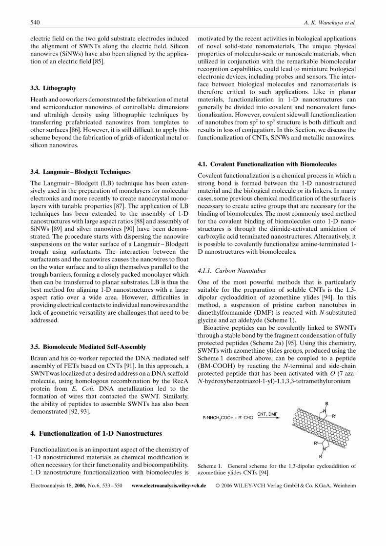
One of the most powerful methods that is particularlysuitable for the preparation of soluble CNTs is the 1,3-dipolar cycloaddition of azomethine ylides [94]. In thismethod, a suspension of pristine carbon nanotubes indimethylformamide (DMF) is reacted with N-substitutedglycine and an aldehyde (Scheme 1).Bioactive peptides can be covalently linked to SWNTs
through a stable bond by the fragment condensation of fullyprotected peptides (Scheme 2a) [95]. Using this chemistry,SWNTs with azomethine ylides groups, produced using theScheme 1 described above, can be coupled to a peptide(BM-COOH) by reacting the N-terminal and side-chainprotected peptide that has been activated with O-(7-aza-N-hydroxybenzotriazol-1-yl)-1,1,3,3-tetramethyluronium
Scheme 1. General scheme for the 1,3-dipolar cycloaddition ofazomethine ylides CNTs [94].
540 A. K. Wanekaya et al.
Electroanalysis 18, 2006, No. 6, 533 – 550 www.electroanalysis.wiley-vch.de C 2006 WILEY-VCH Verlag GmbH&Co. KGaA, Weinheim
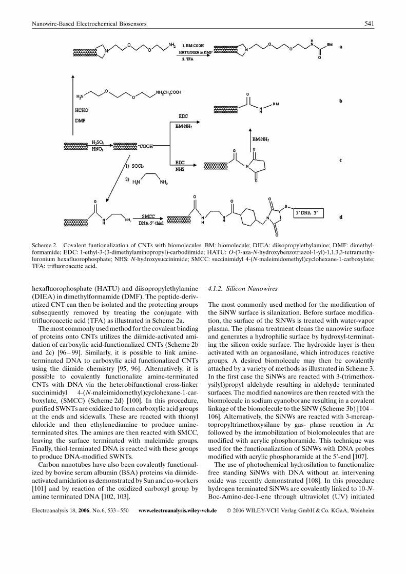
hexafluorophosphate (HATU) and diisopropylethylamine(DIEA) in dimethylformamide (DMF). The peptide-deriv-atized CNT can then be isolated and the protecting groupssubsequently removed by treating the conjugate withtrifluoroacetic acid (TFA) as illustrated in Scheme 2a.Themost commonlyusedmethod for the covalent binding
of proteins onto CNTs utilizes the diimide-activated ami-dation of carboxylic acid-functionalized CNTs (Scheme 2band 2c) [96 – 99]. Similarly, it is possible to link amine-terminated DNA to carboxylic acid functionalized CNTsusing the diimide chemistry [95, 96]. Alternatively, it ispossible to covalently functionalize amine-terminatedCNTs with DNA via the heterobifunctional cross-linkersuccinimidyl 4-(N-maleimidomethyl)cyclohexane-1-car-boxylate, (SMCC) (Scheme 2d) [100]. In this procedure,purified SWNTs are oxidized to form carboxylic acid groupsat the ends and sidewalls. These are reacted with thionylchloride and then ethylenediamine to produce amine-terminated sites. The amines are then reacted with SMCC,leaving the surface terminated with maleimide groups.Finally, thiol-terminated DNA is reacted with these groupsto produce DNA-modified SWNTs.Carbon nanotubes have also been covalently functional-
ized by bovine serum albumin (BSA) proteins via diimide-activated amidation as demonstratedbySun and co-workers[101] and by reaction of the oxidized carboxyl group byamine terminated DNA [102, 103].
4.1.2. Silicon Nanowires
The most commonly used method for the modification ofthe SiNW surface is silanization. Before surface modifica-tion, the surface of the SiNWs is treated with water-vaporplasma. The plasma treatment cleans the nanowire surfaceand generates a hydrophilic surface by hydroxyl-terminat-ing the silicon oxide surface. The hydroxide layer is thenactivated with an organosilane, which introduces reactivegroups. A desired biomolecule may then be covalentlyattached by a variety of methods as illustrated in Scheme 3.In the first case the SiNWs are reacted with 3-(trimethox-ysilyl)propyl aldehyde resulting in aldehyde terminatedsurfaces. The modified nanowires are then reacted with thebiomolecule in sodium cyanoborane resulting in a covalentlinkage of the biomolecule to the SiNW (Scheme 3b) [104 –106]. Alternatively, the SiNWs are reacted with 3-mercap-topropyltrimethoxysilane by gas- phase reaction in Arfollowed by the immobilization of biolomolecules that aremodified with acrylic phosphoramide. This technique wasused for the functionalization of SiNWs with DNA probesmodified with acrylic phosphoramide at the 5N-end [107].The use of photochemical hydrosilation to functionalize
free standing SiNWs with DNA without an interveningoxide was recently demonstrated [108]. In this procedurehydrogen terminated SiNWs are covalently linked to 10-N-Boc-Amino-dec-1-ene through ultraviolet (UV) initiated
Scheme 2. Covalent funtionalization of CNTs with biomolecules. BM: biomolecule; DIEA: diisopropylethylamine; DMF: dimethyl-formamide; EDC: 1-ethyl-3-(3-dimethylaminopropyl)-carbodiimide; HATU: O-(7-aza-N-hydroxybenzotriazol-1-yl)-1,1,3,3-tetramethy-luronium hexafluorophosphate; NHS: N-hydroxysuccinimide; SMCC: succinimidyl 4-(N-maleimidomethyl)cyclohexane-1-carboxylate;TFA: trifluoroacetic acid.
541Nanowire-Based Electrochemical Biosensors
Electroanalysis 18, 2006, No. 6, 533 – 550 www.electroanalysis.wiley-vch.de C 2006 WILEY-VCH Verlag GmbH&Co. KGaA, Weinheim
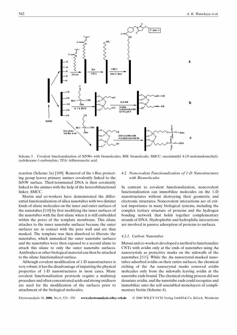
reaction (Scheme 3a) [109]. Removal of the t-Boc protect-ing group leaves primary amines covalently linked to theSiNW surface. Thiol-terminated DNA is then covalentlylinked to the amines with the help of the heterobifunctionallinker, SMCC.Martin and co-workers have demonstrated the differ-
ential functionalization of silica nanotubes with two distinctkinds of silane molecules on the inner and outer surfaces ofthe nanotubes [110] by first modifying the inner surfaces ofthe nanotubes with the first silane when it is still embeddedwithin the pores of the template membrane. This silaneattaches to the inner nanotube surfaces because the outersurfaces are in contact with the pore wall and are thusmasked. The template was then dissolved to liberate thenanotubes, which unmasked the outer nanotube surfacesand the nanotubes were then exposed to a second silane toattach this silane to only the outer nanotube surfaces.Antibodies or other biologicalmaterial can thenbe attachedto the silane functionalized surface.Although covalent modification of 1-D nanostructures is
very robust, it has the disadvantage of impairing the physicalproperties of 1-D nanostructures in most cases. Manycovalent functionalization protocols require a multistepprocedure andoften concentrated acids and strongoxidizersare used for the modification of the surfaces prior toattachment of the biological molecules.
4.2. Noncovalent Functionalization of 1-D Nanostructureswith Biomolecules
In contrast to covalent functionalization, noncovalentfunctionalization can immobilize molecules on the 1-Dnanostructures without destroying their geometric andelectronic structures. Noncovalent interactions are of crit-ical importance in many biological systems, including thecomplex tertiary structure of proteins and the hydrogenbonding network that holds together complementarystrands of DNA. Hydrophobic and hydrophilic interactionsare involved in passive adsorption of proteins to surfaces.
4.2.1. Carbon Nanotubes
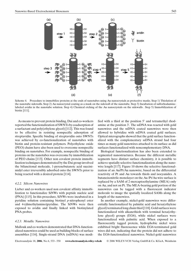
Matsui and co-workers developed amethod to functionalizeCNTs with avidin only at the ends of nanotubes using Aunanocrystals as protective masks on the sidewalls of thenanotubes [111]. While the Au nanocrystal-masked nano-tubes adsorbed avidin on their entire surfaces, the chemicaletching of the Au nanocrystal masks removed avidinmolecules only from the sidewalls leaving avidin at thenanotube ends bound. The chemical etching process did notdenature avidin, and the nanotube ends could recognize andimmobilize onto the self-assembled monolayers of compli-mentary biotin (Scheme 4).
Scheme 3. Covalent functionalization of SiNWs with biomolecules. BM: biomolecule; SMCC: succinimidyl 4-(N-maleimidomethyl)-cyclohexane-1-carboxylate; TFA: trifluoroacetic acid.
542 A. K. Wanekaya et al.
Electroanalysis 18, 2006, No. 6, 533 – 550 www.electroanalysis.wiley-vch.de C 2006 WILEY-VCH Verlag GmbH&Co. KGaA, Weinheim
Asmeans to prevent protein binding, Dai and co-workersreported the functionalizationof SWNTsby coadsorptionofa surfactant and poly(ethylene glycol) [112]. This was foundto be effective in resisting nonspecific adsorption ofstreptavidin. Specific binding of streptavidin onto SWNTswas achieved by co-functionalization of nanotubes withbiotin and protein-resistant polymers. Polyethylene oxide(PEO) chains have also been used to overcome nonspecificbinding on nanotubes. For example, nonspecific binding ofproteins on the nanotubes was overcome by immobilizationof PEO chains [113]. Other non covalent protein immobi-lization techniques demonstrated by theDai group involvedthe bifunctional molecule, 1-pyrenebutanoic acid succini-midyl ester irreversibly adsorbed onto the SWNTs prior tobeing reacted with a desired protein [114].
4.2.2. Silicon Nanowires
Lieber and co-workers used non covalent affinity immobi-lization to functionalize SiNWs with peptide nucleic acid(PNA) [115]. In this procedure, SiNWs were incubated in apyridine solution containing biotinyl p-nitrophenyl esterand 4-(dimethylamino)pyridine. The SiNWs were thenexposed to avidin and finally linked with biotinylatedPNA probes.
4.2.3. Metallic Nanowires
Mallouk and co-workers demonstrated that DNA-function-alized nanowires could be used as building blocks of surfaceassemblies [116]. Single-strand DNA (ssDNA) was modi-
fied with a thiol at the position 5N and tetramethyl rhod-amine at the position 3’. The ssDNAwas reacted with goldnanowires and the ssDNA coated nanowires were thenallowed to hybridize with ssDNA coated gold surfaces.Optical micrographs showed that the gold surface function-alized with the complementary ssDNA strand had fourtimes as many gold nanowires attached to its surface as didsurfaces functionalized with noncomplementary DNA.Biological functionalization has also been extended to
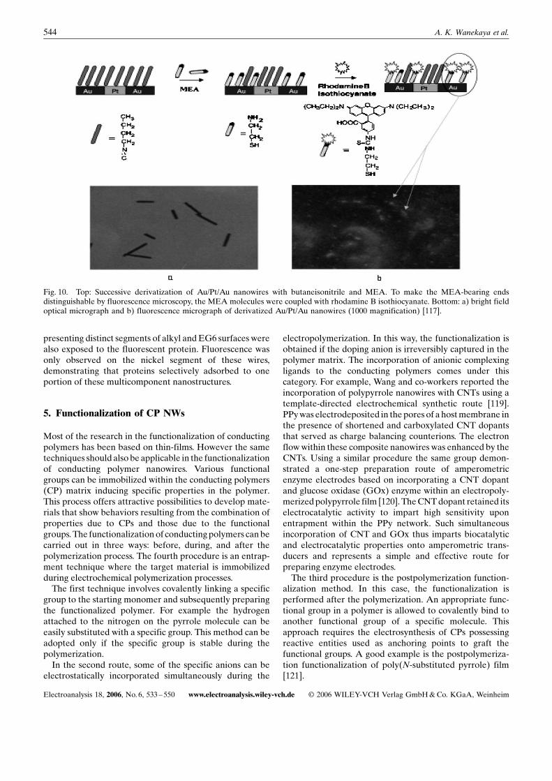
segmented nanostructures. Because the different metallicsegments have distinct surface chemistry, it is possible toachieve spatially selective functionalization along the nano-wire length [117]. Figure 10 shows the selective functional-ization of an Au/Pt/Au nanowire, based on the differentialreactivity of Pt and Au towards thiols and isocyanides. Abutaneisonitrile monolayer on the Au /Pt/Au wire surface isreplaced by a SAM of 2-mercaptoethylamine (MEA) onlyonAu, and not on Pt. TheMEA-bearing gold portion of thenanowires can be tagged with a fluorescent indicatormolecule to image the spatially localized SAMs along thelength of the nanowires.In another example, nickel-gold nanowires were differ-
entially functionalized by palmitic acid and hexa(ethyleneglycol) terminated long chain thiol [118].Gold surfaceswerefunctionalized with alkanethiols with terminal hexa(ethy-lene glycol) groups (EG6), while nickel surfaces werefunctionalized with palmitic acid. When exposed to afluorescently tagged protein, hydrophobic nickel wiresexhibited bright fluorescence while EG6-terminated goldwires did not, indicating that the protein did not adhere tothe EG6-functionalized nanowires. Nickel-gold nanowires
Scheme 4. Procedure to immobilize proteins at the ends of nanotubes using Au nanocrystals as protective masks. Step 1) Thiolation ofthe nanotube sidewalls. Step 2) Au nanocrystal coating as a mask on the sidewall of the nanotube. Step 3) Incubation of sulforhodamine-labeled avidin in the nanotube solution. Step 4) Chemical etching of the Au nanocrystals on the sidewalls . Step 5) Immobilization ofbiotin [111].
543Nanowire-Based Electrochemical Biosensors
Electroanalysis 18, 2006, No. 6, 533 – 550 www.electroanalysis.wiley-vch.de C 2006 WILEY-VCH Verlag GmbH&Co. KGaA, Weinheim
presenting distinct segments of alkyl andEG6 surfaces werealso exposed to the fluorescent protein. Fluorescence wasonly observed on the nickel segment of these wires,demonstrating that proteins selectively adsorbed to oneportion of these multicomponent nanostructures.
5. Functionalization of CP NWs
Most of the research in the functionalization of conductingpolymers has been based on thin-films. However the sametechniques should also be applicable in the functionalizationof conducting polymer nanowires. Various functionalgroups can be immobilized within the conducting polymers(CP) matrix inducing specific properties in the polymer.This process offers attractive possibilities to develop mate-rials that show behaviors resulting from the combination ofproperties due to CPs and those due to the functionalgroups.The functionalizationof conductingpolymers canbecarried out in three ways: before, during, and after thepolymerization process. The fourth procedure is an entrap-ment technique where the target material is immobilizedduring electrochemical polymerization processes.The first technique involves covalently linking a specific
group to the starting monomer and subsequently preparingthe functionalized polymer. For example the hydrogenattached to the nitrogen on the pyrrole molecule can beeasily substituted with a specific group. This method can beadopted only if the specific group is stable during thepolymerization.In the second route, some of the specific anions can be
electrostatically incorporated simultaneously during the
electropolymerization. In this way, the functionalization isobtained if the doping anion is irreversibly captured in thepolymer matrix. The incorporation of anionic complexingligands to the conducting polymers comes under thiscategory. For example, Wang and co-workers reported theincorporation of polypyrrole nanowires with CNTs using atemplate-directed electrochemical synthetic route [119].PPywas electrodeposited in the pores of a hostmembrane inthe presence of shortened and carboxylated CNT dopantsthat served as charge balancing counterions. The electronflowwithin these composite nanowires was enhanced by theCNTs. Using a similar procedure the same group demon-strated a one-step preparation route of amperometricenzyme electrodes based on incorporating a CNT dopantand glucose oxidase (GOx) enzyme within an electropoly-merizedpolypyrrole film [120]. TheCNTdopant retained itselectrocatalytic activity to impart high sensitivity uponentrapment within the PPy network. Such simultaneousincorporation of CNT and GOx thus imparts biocatalyticand electrocatalytic properties onto amperometric trans-ducers and represents a simple and effective route forpreparing enzyme electrodes.The third procedure is the postpolymerization function-
alization method. In this case, the functionalization isperformed after the polymerization. An appropriate func-tional group in a polymer is allowed to covalently bind toanother functional group of a specific molecule. Thisapproach requires the electrosynthesis of CPs possessingreactive entities used as anchoring points to graft thefunctional groups. A good example is the postpolymeriza-tion functionalization of poly(N-substituted pyrrole) film[121].
Fig. 10. Top: Successive derivatization of Au/Pt/Au nanowires with butaneisonitrile and MEA. To make the MEA-bearing endsdistinguishable by fluorescence microscopy, the MEA molecules were coupled with rhodamine B isothiocyanate. Bottom: a) bright fieldoptical micrograph and b) fluorescence micrograph of derivatized Au/Pt/Au nanowires (1000 magnification) [117].
544 A. K. Wanekaya et al.
Electroanalysis 18, 2006, No. 6, 533 – 550 www.electroanalysis.wiley-vch.de C 2006 WILEY-VCH Verlag GmbH&Co. KGaA, Weinheim
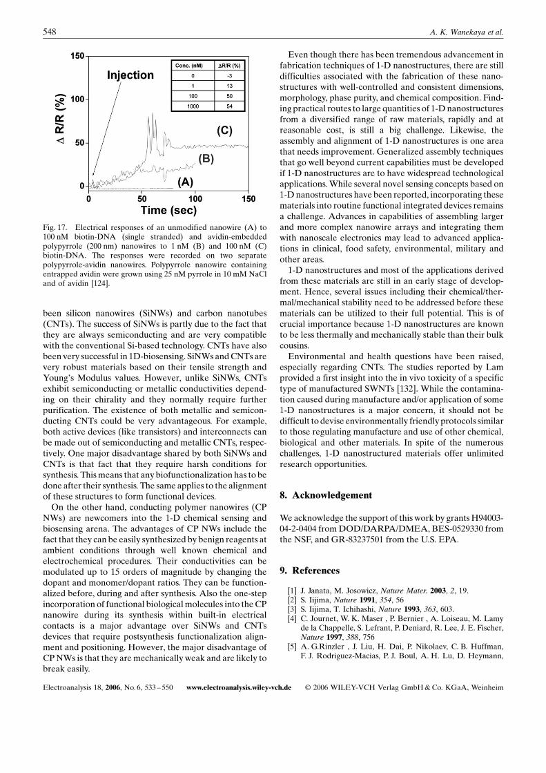
The fourth way involves entrapment of target moleculeswithin conducting polymers. This route involves the appli-cation of an appropriate potential to the working electrodesoaked a solution containing the target molecule, themonomer and dopant. However, in some cases, physicalentrapment and steric, hindrances may drastically reducethe catalytic activity and flexibility of some immobilizedbiomolecules such as enzymes as observed in polymer films[122, 123].On the other hand, an advantage of thismethod isthat entrapment of the molecules occurs without anychemical reaction that could affect their activity. Forexample we recently entrapped biological molecules withinconducting polymer nanowires using a procedure that issafe, fast and convenient [124]. In this process, avidin wasentrapped during the electrochemical polymerization ofpolypyrrole in a single step protocol within a 100 nm-widechannel connecting 2 electrodes resulting in avidin-func-tionalized CP NWof controlled dimensions and high aspectratio. Similarly, Mallouk and co-workers reported thefabrication of gold-capped, protein-modified polypyrrolenanowires using a porous aluminum oxide template [125].
6. Applications of 1-D Nanostructures in Biosensing
6.1. Protein Detection
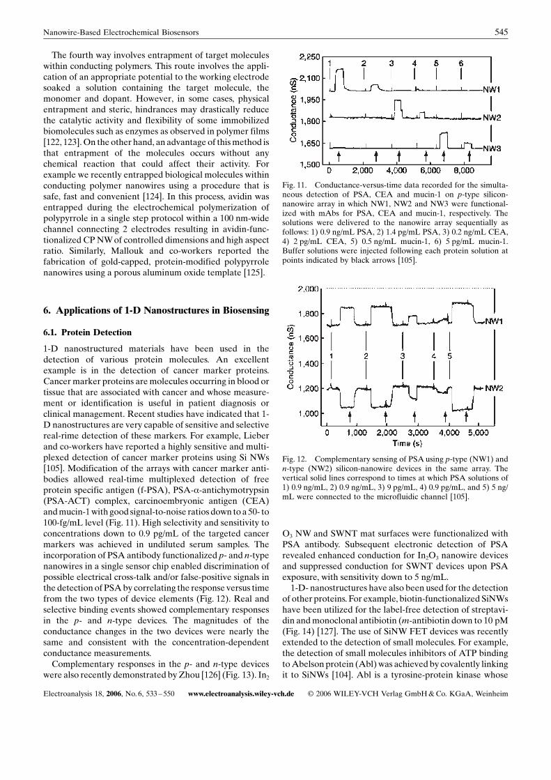
1-D nanostructured materials have been used in thedetection of various protein molecules. An excellentexample is in the detection of cancer marker proteins.Cancer marker proteins aremolecules occurring in blood ortissue that are associated with cancer and whose measure-ment or identification is useful in patient diagnosis orclinical management. Recent studies have indicated that 1-D nanostructures are very capable of sensitive and selectivereal-rime detection of these markers. For example, Lieberand co-workers have reported a highly sensitive and multi-plexed detection of cancer marker proteins using Si NWs[105]. Modification of the arrays with cancer marker anti-bodies allowed real-time multiplexed detection of freeprotein specific antigen (f-PSA), PSA-a-antichymotrypsin(PSA-ACT) complex, carcinoembryonic antigen (CEA)andmucin-1with good signal-to-noise ratios down toa 50- to100-fg/mL level (Fig. 11). High selectivity and sensitivity toconcentrations down to 0.9 pg/mL of the targeted cancermarkers was achieved in undiluted serum samples. Theincorporation of PSA antibody functionalized p- and n-typenanowires in a single sensor chip enabled discrimination ofpossible electrical cross-talk and/or false-positive signals inthe detection of PSAby correlating the response versus timefrom the two types of device elements (Fig. 12). Real andselective binding events showed complementary responsesin the p- and n-type devices. The magnitudes of theconductance changes in the two devices were nearly thesame and consistent with the concentration-dependentconductance measurements.Complementary responses in the p- and n-type devices
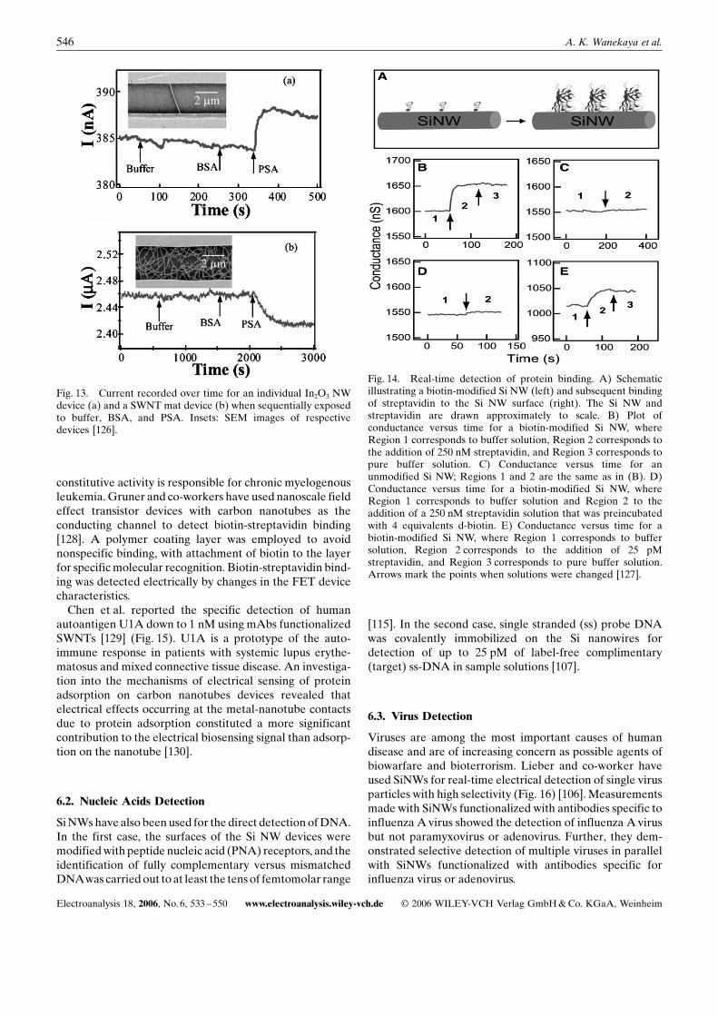
were also recently demonstrated byZhou [126] (Fig. 13). In2
O3 NW and SWNT mat surfaces were functionalized withPSA antibody. Subsequent electronic detection of PSArevealed enhanced conduction for In2O3 nanowire devicesand suppressed conduction for SWNT devices upon PSAexposure, with sensitivity down to 5 ng/mL.1-D- nanostructures have also been used for the detection
of other proteins. For example, biotin-functionalized SiNWshave been utilized for the label-free detection of streptavi-din andmonoclonal antibiotin (m-antibiotin down to 10 pM(Fig. 14) [127]. The use of SiNW FET devices was recentlyextended to the detection of small molecules. For example,the detection of small molecules inhibitors of ATP bindingtoAbelson protein (Abl) was achieved by covalently linkingit to SiNWs [104]. Abl is a tyrosine-protein kinase whose
Fig. 11. Conductance-versus-time data recorded for the simulta-neous detection of PSA, CEA and mucin-1 on p-type silicon-nanowire array in which NW1, NW2 and NW3 were functional-ized with mAbs for PSA, CEA and mucin-1, respectively. Thesolutions were delivered to the nanowire array sequentially asfollows: 1) 0.9 ng/mL PSA, 2) 1.4 pg/mL PSA, 3) 0.2 ng/mL CEA,4) 2 pg/mL CEA, 5) 0.5 ng/mL mucin-1, 6) 5 pg/mL mucin-1.Buffer solutions were injected following each protein solution atpoints indicated by black arrows [105].
Fig. 12. Complementary sensing of PSAusing p-type (NW1) andn-type (NW2) silicon-nanowire devices in the same array. Thevertical solid lines correspond to times at which PSA solutions of1) 0.9 ng/mL, 2) 0.9 ng/mL, 3) 9 pg/mL, 4) 0.9 pg/mL, and 5) 5 ng/mL were connected to the microfluidic channel [105].
545Nanowire-Based Electrochemical Biosensors
Electroanalysis 18, 2006, No. 6, 533 – 550 www.electroanalysis.wiley-vch.de C 2006 WILEY-VCH Verlag GmbH&Co. KGaA, Weinheim
constitutive activity is responsible for chronic myelogenousleukemia. Gruner and co-workers have used nanoscale fieldeffect transistor devices with carbon nanotubes as theconducting channel to detect biotin-streptavidin binding[128]. A polymer coating layer was employed to avoidnonspecific binding, with attachment of biotin to the layerfor specific molecular recognition. Biotin-streptavidin bind-ing was detected electrically by changes in the FET devicecharacteristics.Chen et al. reported the specific detection of human
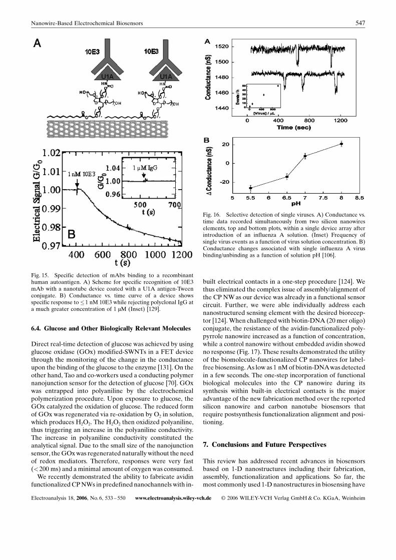
autoantigen U1A down to 1 nM using mAbs functionalizedSWNTs [129] (Fig. 15). U1A is a prototype of the auto-immune response in patients with systemic lupus erythe-matosus and mixed connective tissue disease. An investiga-tion into the mechanisms of electrical sensing of proteinadsorption on carbon nanotubes devices revealed thatelectrical effects occurring at the metal-nanotube contactsdue to protein adsorption constituted a more significantcontribution to the electrical biosensing signal than adsorp-tion on the nanotube [130].
6.2. Nucleic Acids Detection
SiNWshave also beenused for the direct detection ofDNA.In the first case, the surfaces of the Si NW devices weremodifiedwith peptide nucleic acid (PNA) receptors, and theidentification of fully complementary versus mismatchedDNAwas carried out to at least the tens of femtomolar range
[115]. In the second case, single stranded (ss) probe DNAwas covalently immobilized on the Si nanowires fordetection of up to 25 pM of label-free complimentary(target) ss-DNA in sample solutions [107].
6.3. Virus Detection
Viruses are among the most important causes of humandisease and are of increasing concern as possible agents ofbiowarfare and bioterrorism. Lieber and co-worker haveused SiNWs for real-time electrical detection of single virusparticles with high selectivity (Fig. 16) [106]. Measurementsmade with SiNWs functionalized with antibodies specific toinfluenza Avirus showed the detection of influenza Avirusbut not paramyxovirus or adenovirus. Further, they dem-onstrated selective detection of multiple viruses in parallelwith SiNWs functionalized with antibodies specific forinfluenza virus or adenovirus.
Fig. 13. Current recorded over time for an individual In2O3 NWdevice (a) and a SWNT mat device (b) when sequentially exposedto buffer, BSA, and PSA. Insets: SEM images of respectivedevices [126].
Fig. 14. Real-time detection of protein binding. A) Schematicillustrating a biotin-modified Si NW (left) and subsequent bindingof streptavidin to the Si NW surface (right). The Si NW andstreptavidin are drawn approximately to scale. B) Plot ofconductance versus time for a biotin-modified Si NW, whereRegion 1 corresponds to buffer solution, Region 2 corresponds tothe addition of 250 nM streptavidin, and Region 3 corresponds topure buffer solution. C) Conductance versus time for anunmodified Si NW; Regions 1 and 2 are the same as in (B). D)Conductance versus time for a biotin-modified Si NW, whereRegion 1 corresponds to buffer solution and Region 2 to theaddition of a 250 nM streptavidin solution that was preincubatedwith 4 equivalents d-biotin. E) Conductance versus time for abiotin-modified Si NW, where Region 1 corresponds to buffersolution, Region 2 corresponds to the addition of 25 pMstreptavidin, and Region 3 corresponds to pure buffer solution.Arrows mark the points when solutions were changed [127].
546 A. K. Wanekaya et al.
Electroanalysis 18, 2006, No. 6, 533 – 550 www.electroanalysis.wiley-vch.de C 2006 WILEY-VCH Verlag GmbH&Co. KGaA, Weinheim
6.4. Glucose and Other Biologically Relevant Molecules
Direct real-time detection of glucose was achieved by usingglucose oxidase (GOx) modified-SWNTs in a FET devicethrough the monitoring of the change in the conductanceupon the binding of the glucose to the enzyme [131]. On theother hand, Tao and co-workers used a conducting polymernanojunction sensor for the detection of glucose [70]. GOxwas entrapped into polyaniline by the electrochemicalpolymerization procedure. Upon exposure to glucose, theGOx catalyzed the oxidation of glucose. The reduced formof GOx was regenerated via re-oxidation by O2 in solution,which produces H2O2. The H2O2 then oxidized polyaniline,thus triggering an increase in the polyaniline conductivity.The increase in polyaniline conductivity constituted theanalytical signal. Due to the small size of the nanojunctionsensor, theGOxwas regenerated naturallywithout the needof redox mediators. Therefore, responses were very fast(<200 ms) and aminimal amount of oxygen was consumed.We recently demonstrated the ability to fabricate avidin
functionalizedCPNWs in predefined nanochannels with in-
built electrical contacts in a one-step procedure [124]. Wethus eliminated the complex issue of assembly/alignment ofthe CP NWas our device was already in a functional sensorcircuit. Further, we were able individually address eachnanostructured sensing element with the desired biorecep-tor [124]. When challenged with biotin-DNA (20 mer oligo)conjugate, the resistance of the avidin-functionalized poly-pyrrole nanowire increased as a function of concentration,while a control nanowire without embedded avidin showedno response (Fig. 17). These results demonstrated the utilityof the biomolecule-functionalized CP nanowires for label-free biosensing.As low as 1 nMof biotin-DNAwas detectedin a few seconds. The one-step incorporation of functionalbiological molecules into the CP nanowire during itssynthesis within built-in electrical contacts is the majoradvantage of the new fabrication method over the reportedsilicon nanowire and carbon nanotube biosensors thatrequire postsynthesis functionalization alignment and posi-tioning.
7. Conclusions and Future Perspectives
This review has addressed recent advances in biosensorsbased on 1-D nanostructures including their fabrication,assembly, functionalization and applications. So far, themost commonly used 1-D nanostructures in biosensing have
Fig. 15. Specific detection of mAbs binding to a recombinanthuman autoantigen. A) Scheme for specific recognition of 10E3mAb with a nanotube device coated with a U1A antigen-Tweenconjugate. B) Conductance vs. time curve of a device showsspecific response to �1 nM 10E3 while rejecting polyclonal IgG ata much greater concentration of 1 mM (Inset) [129].
Fig. 16. Selective detection of single viruses. A) Conductance vs.time data recorded simultaneously from two silicon nanowireselements, top and bottom plots, within a single device array afterintroduction of an influenza A solution. (Inset) Frequency ofsingle virus events as a function of virus solution concentration. B)Conductance changes associated with single influenza A virusbinding/unbinding as a function of solution pH [106].
547Nanowire-Based Electrochemical Biosensors
Electroanalysis 18, 2006, No. 6, 533 – 550 www.electroanalysis.wiley-vch.de C 2006 WILEY-VCH Verlag GmbH&Co. KGaA, Weinheim
been silicon nanowires (SiNWs) and carbon nanotubes(CNTs). The success of SiNWs is partly due to the fact thatthey are always semiconducting and are very compatiblewith the conventional Si-based technology. CNTs have alsobeen very successful in 1D-biosensing. SiNWs andCNTs arevery robust materials based on their tensile strength andYoungNs Modulus values. However, unlike SiNWs, CNTsexhibit semiconducting or metallic conductivities depend-ing on their chirality and they normally require furtherpurification. The existence of both metallic and semicon-ducting CNTs could be very advantageous. For example,both active devices (like transistors) and interconnects canbe made out of semiconducting and metallic CNTs, respec-tively. One major disadvantage shared by both SiNWs andCNTs is that fact that they require harsh conditions forsynthesis. Thismeans that any biofunctionalization has to bedone after their synthesis. The same applies to the alignmentof these structures to form functional devices.On the other hand, conducting polymer nanowires (CP
NWs) are newcomers into the 1-D chemical sensing andbiosensing arena. The advantages of CP NWs include thefact that they can be easily synthesized by benign reagents atambient conditions through well known chemical andelectrochemical procedures. Their conductivities can bemodulated up to 15 orders of magnitude by changing thedopant and monomer/dopant ratios. They can be function-alized before, during and after synthesis. Also the one-stepincorporation of functional biologicalmolecules into theCPnanowire during its synthesis within built-in electricalcontacts is a major advantage over SiNWs and CNTsdevices that require postsynthesis functionalization align-ment and positioning. However, the major disadvantage ofCPNWs is that they aremechanically weak and are likely tobreak easily.
Even though there has been tremendous advancement infabrication techniques of 1-D nanostructures, there are stilldifficulties associated with the fabrication of these nano-structures with well-controlled and consistent dimensions,morphology, phase purity, and chemical composition. Find-ing practical routes to large quantities of 1-Dnanostructuresfrom a diversified range of raw materials, rapidly and atreasonable cost, is still a big challenge. Likewise, theassembly and alignment of 1-D nanostructures is one areathat needs improvement. Generalized assembly techniquesthat go well beyond current capabilities must be developedif 1-D nanostructures are to have widespread technologicalapplications.While several novel sensing concepts based on1-Dnanostructures have been reported, incorporating thesematerials into routine functional integrated devices remainsa challenge. Advances in capabilities of assembling largerand more complex nanowire arrays and integrating themwith nanoscale electronics may lead to advanced applica-tions in clinical, food safety, environmental, military andother areas.1-D nanostructures and most of the applications derived
from these materials are still in an early stage of develop-ment. Hence, several issues including their chemical/ther-mal/mechanical stability need to be addressed before thesematerials can be utilized to their full potential. This is ofcrucial importance because 1-D nanostructures are knownto be less thermally and mechanically stable than their bulkcousins.Environmental and health questions have been raised,
especially regarding CNTs. The studies reported by Lamprovided a first insight into the in vivo toxicity of a specifictype of manufactured SWNTs [132]. While the contamina-tion caused during manufacture and/or application of some1-D nanostructures is a major concern, it should not bedifficult to devise environmentally friendly protocols similarto those regulating manufacture and use of other chemical,biological and other materials. In spite of the numerouschallenges, 1-D nanostructured materials offer unlimitedresearch opportunities.
8. Acknowledgement
Weacknowledge the support of this work by grantsH94003-04-2-0404 fromDOD/DARPA/DMEA, BES-0529330 fromthe NSF, and GR-83237501 from the U.S. EPA.
9. References
[1] J. Janata, M. Josowicz, Nature Mater. 2003, 2, 19.[2] S. Iijima, Nature 1991, 354, 56[3] S. Iijima, T. Ichihashi, Nature 1993, 363, 603.[4] C. Journet, W. K. Maser , P. Bernier , A. Loiseau, M. Lamy
de la Chappelle, S. Lefrant, P. Deniard, R. Lee, J. E. Fischer,Nature 1997, 388, 756
[5] A. G.Rinzler , J. Liu, H. Dai, P. Nikolaev, C. B. Huffman,F. J. Rodriguez-Macias, P. J. Boul, A. H. Lu, D. Heymann,
Fig. 17. Electrical responses of an unmodified nanowire (A) to100 nM biotin-DNA (single stranded) and avidin-embeddedpolypyrrole (200 nm) nanowires to 1 nM (B) and 100 nM (C)biotin-DNA. The responses were recorded on two separatepolypyrrole-avidin nanowires. Polypyrrole nanowire containingentrapped avidin were grown using 25 nM pyrrole in 10 mM NaCland of avidin [124].
548 A. K. Wanekaya et al.
Electroanalysis 18, 2006, No. 6, 533 – 550 www.electroanalysis.wiley-vch.de C 2006 WILEY-VCH Verlag GmbH&Co. KGaA, Weinheim
D. T .Colbert, R. S. Lee, J. E. Fischer, A. M. Rao, P. C.Eklund, R. E. Smalley, Appl. Phys. A 1998, 67, 29.
[6] P. Nikolaev, M. J. Bronikowski, R. K. Bradley, F. Rohmund,D. T. Colbert, K. A. Smith, R. E.Smalley, Chem. Phys. Lett.1999, 313, 91.
[7] Z. F. Ren, Z. P. Huang, J. W. Xu, D. Z. Wang, J. G. Wen,J. H.Wang, Appl. Phys. Lett. 1999, 75, 1086.
[8] Z. F. Ren, Z. P. Huang, J. W. Xu, J. H. Wang, P. Bush andM. P.Siegal, P. N. Provencio, Science 1998, 282, 1105.
[9] Z. P. Huang, J. W. Xu, Z. F. Ren, J. H. Wang, M. P. Siegal ,P. N. Provencio , Appl. Phys. Lett. 1998, 73, 3845.
[10] D. S. Bethune, C. H. Kiang, M. S. Devries, G. Gorman, R.Savoy, J. Vazquez, Nature 1993, 363, 605.
[11] Z. Shi, Y. Lian, F. H. Liao, X. Zhou, Z. Gu and Y Zhang, J.Phys. Chem. Solids 2000, 61, 1031.
[12] Y. Saito, K. Nishikubo, K. Kawabata, T. Matsumoto, J. App.Phys. 1996, 80, 3062.
[13] A. Thess, R. Lee, P. Nikolaev, H. J. Dai, P. Petit, J. Robert,Science 1996, 273, 483.
[14] Y. Zhang and S. Iijima, Appl. Phys. Lett. 1999, 75, 3087.[15] M. Ge, K. Sattler, Appl. Phys. Lett. 1994, 64, 710.[16] G. Che, B. B. Lakshmi, C. R. Martin, E. R. Fisher, R. S.
Ruoff, Chem. Mater. 1998, 10, 260.[17] W. Z. Li, S. S. Xie, L. X. Qian, B. H. Chang, B. S. Zou, W.Y
Zho, Science 1999, 274, 1701.[18] X. X. Zhang, Z. Q. Li, G. H. Wen, K. K. Fung, J. Chen, Y.
Li, Chem. Phys. Lett. 2001, 333, 509.[19] D. P. Yu, Z. G. Bai, Y. Ding, Q. L. Hang, H. Z. Zhang, J. J.
Wang, Y. H. Zou, W. Qian, G. C. Xiong, H. T. Zhou andS. Q. Feng. Appl. Phys. Lett., 1998, 72, 3458.
[20] M. K. Sunkara, S. Sharma, R. Miranda, G. Lian, E. C.Dickey. Appl. Phys. Lett. 2001, 79, 1546.
[21] R. S. Wagner, W. C. Ellis, Appl. Phys. Lett. 1964, 4, 89.[22] Y. Wu, P. Yang, Chem. Mater. 2000, 12, 605.[23] Y. J. Zhang, Q. Zhang, N. L.Wang, Y. J. Yan, H. H. Zhou, J.
Zhu, J. Cryst. Growth 2001, 226, 185.[24] J. Westwater, D. P. Gosain, S. Tomiya, S. Usui, H. Ruda, J.
Vac. Sci. Technol. B 1997, 15, 554.[25] Y. Wu, P.Yang, J. Am. Chem. Soc. 2001, 123, 3165.[26] M. S. Gudiksen, C. M. Lieber J. Am. Chem. Soc. 2000, 122,
8801.[27] Y. Wu, H. Yan, M. Huang, B. Messer, J. H. Song, P. Yang,
Chem. Eur. J. 2002, 8, 1260.[28] X. Duan, C. M. Lieber, Adv. Mater. 2000, 12, 298.[29] C. C. Chen, C. C. Yeh, C. H. Chen, M. Y. Yu, H. L. Liu, J.
Am. Chem. Soc. 2001, 123, 2791.[30] J. Zhang, X. S. Peng, X. F. Wang, Y. W., L. D. Zhang, Chem.
Phys. Lett. 2001, 345,372.[31] M. Pe, P. Zhou, S. N. Mohammad, G. L. Harris, J. B.
Halpern, J. Cryst. Growth 2001, 231, 357.[32] W. S. Shi, Y. F. Zheng, N. Wang, C. S. Lee, S. T. Lee, J. Vac.
Sci. Technol. B 2001, 19, 1115.[33] Y. Cui, L. J. Lauhon, M. S. Gudisen, J. Wang, C. M. Lieber.
Appl. Phys. Lett. 2001, 78, 2214.[34] J. Westwater, D. P. Gosain, S. Usui, H. Ruda. Phys. Status
Solidi A 1998, 165, 37.[35] T. E. Bogart, S. Dey, K.-K. Lew, S. E. Mohney, J. M.
Redwing, Adv. Mater. 2005, 17, 114.[36] K.-K. Lew, C. Reuther, A. H. Carim, J. M. Redwing, J. Vac.
Sci. Technol. B 2002, 20, 389.[37] J. D. Holmes, K. P. Johnston, R. C. Doty, B. A. Korgel,
Science 2000, 287, 1471.[38] Y. F. Zhang, Y. H. Tang, N. Wang, D. P. Yu, C. S. Lee, I.
Bello, S. T. Lee, Appl. Phys. Lett. 1998, 72, 1835.[39] Y. F. Zhang, Y. H. Tang, H. Y. Peng, N. Wang, C. S. Lee, I.
Bello, S. T. Lee. Appl. Phys. Lett. 1999, 75, 1842.[40] A. M. Morales, C. M. Lieber, Science 1998, 279, 208.
[41] N. Wang, Y. F. Zhang, Y. H. Tang, C. S. Lee and S. T. Lee,Appl. Phys. Lett. 1998, 73, 3902.
[42] N. Wang, Y. H. Tang, Y. F. Zhang, C. S. Lee, S. T. Lee, Phys.Rev. B. 1998, 58, R16024.
[43] Y. F. Zhang, Y. H. Tang, N. Wang, C. S. Lee, I. Bello, S. T.Lee. J. Cryst. Growth 1999, 197, 136.
[44] W. S. Shi, H. Y. Peng, Y. F. Zhang, N. Wang, N. G. Shang,Z. W. Pan, C. S. Lee, S. T. Lee, Adv. Mater. 2000, 12,1343.
[45] Z. Zhang, X. H. Fan, L. Xu, C. S. Lee, S. T. Lee, Chem.Phys. Lett. 2001, 337, 18.
[46] H. Y. Peng, Z. W. Pan, L. Xu, X. H. Fan, N. Wang, C. S. Lee,S. T. Lee. Adv. Mater. 2001, 13, 317.
[47] C. P. Li, X. H. Sun, N. B. Wong, C. S. Lee, S. T. Lee andB. K. Teo. Chem Phys Lett 2002, 365, 22.
[48] H. X. He, C. Z. Li, N. J. Tao, Appl. Phys. Lett. 2001, 78, 811.[49] J. Doshi, D. H. Reneker, J. Electrostatics 1999, 35,151.[50] D. H. Reneker, A. L. Yarin, H. Fong, S. Koombhongse, J.
Appl. Phys. 2000, 87, 4531.[51] C. Jerome, R. Jerome, Angew. Chem. Int. Ed. 1998, 37, 2488.[52] J.-H. Lim, C. A. Mirkin, Adv. Mater. 2002, 14, 1474.[53] B. W. Maynor, S. F. Filocamo, M. W. Grinstaff, J. Liu, J. Am.
Chem. Soc. 2002, 124, 522.[54] J. Kameoka, H. G. Craighead, Appl. Phys. Lett. 2003, 83,
371.[55] J. Kameoka, R. Orth, Y. Yang, D. Czaplewski, R. Mathers,
G. W. Coates, H. G. Craighead, Nanotechnology 2003, 14,1124.
[56] H. Liu, J. Kameoka, D. A. Czaplewski, H. G. Craighead,Nano Lett. 2004, 4, 671.
[57] C. R. Martin, Chem. Mater. 1996, 8, 1739.[58] R. V. Parthasarathy, C. R. Martin, Chem. Mater. 1994, 6,
1627[59] J. P. Spatz, B. Lorenz, K. Weishaupt, H. D. Hochheimer,
V. P. Menon, R. V. Parthasarathy, C. R. Martin, J. Bechtold,P-H. Hor, Phys. Rev. Lett. 1994, 50, 14888.
[60] L. Liang, J. Liu, C. F. Windisch Jr., G. J. Exarhos, Y. Lin,Ang. Chem. Int. Ed. 2002, 41, 3665.
[61] Y. F. Ma, J. M. Zhang, G. J. Zhang, H. X. He, J. Am. Chem.Soc. 2004, 22, 7097.
[62] A. Bensimon, A. Simon, A. Chiffaudel, V. Croquette, F.Heslot, D. Bensimon, Science 1994, 265, 2096.
[63] H. Nakao, H. Hayashi, T. Yoshino, S. Sugiyama, K. Otobe,T. Ohtani, Nano Lett. 2002, 2, 475.
[64] P. Nickels, W. U. Dittmer, S. Beyer, J. P. Kotthaus, F.Simmel, Nanotechnology 2004, 15, 1524.
[65] J. Kong, N. R. Franklin, C. W. Zhou, M. G. Chapline, S.Peng, K. J. Cho, H. Dai, Science 2000, 287, 622.
[66] C. Z. Li, H. X. He, A. Bogozi, J. S. Bunch, N. J. Tao, Appl.Phys. Lett. 2000, 76, 1333.
[67] F. Favier, E. C. Walter, M. P. Zach, T. Benter, R. M. Penner,Science 2001, 293, 2227.
[68] K. Ramanathan, M. A. Banger, M. Yun, W. Chen, A.Mulchandani, N. V. Myung, Nano Lett. 2004, 4, 1237.
[69] M. Yun, N. V. Myung, R. P. Vasquez, E. Menke, R. M.Penner, Nano Lett. 2004, 4, 419.
[70] E. S. Forzani, H. Zhang, L. A. Nagahara, I. Amlani, R. Tsui,N. Tao, Nano Lett. 2004, 4, 1785.
[71] C. Hangarter, N. V. Myung, Chem. Mater. 2005, 17, 1320.[72] A. K. Bentley, J. S. Tretheway, A. B. Ellis, W. S. Crone,
Nano Lett. 2004, 4, 487.[73] S. Niyogi, C. Hangarter, R. M. Thamankar, Y.-F. Chung, R.
Kawakami, N. V. Myung, R. Haddon, J. Phys. Chem. 2004,108, 19818.
[74] M. Tanase, D. M Silevitch, A. Hultgren, L. A. Bauer, P. C.Searson, G. J. Meyer, D. H. Reich, J. Appl. Phys. 2002, 91,8549
549Nanowire-Based Electrochemical Biosensors
Electroanalysis 18, 2006, No. 6, 533 – 550 www.electroanalysis.wiley-vch.de C 2006 WILEY-VCH Verlag GmbH&Co. KGaA, Weinheim
[75] M. Tanase, L. A. Bauer, A. Hultgren, D. M. Silevitch, L.Sun, D. H. Reich, P. C. Searson, G. J. Meyer, Nano Lett.2001, 1, 155.
[76] M. Tanase, E. J. Felton, D. S. Gray, A. Hultgren, C. S. Chen,D. H. Reich, Lab on a Chip, 2005, 5, 598.
[77] H. Zhang, S. Boussaad, N. Ly, N. J. Tao, Appl. Phys. Lett.2004, 84, 134.
[78] C. L. Chien, L. Sun, M. Tanase, L. A. Bauer, A. Hultgren,D. M. Silevitch, G. J. Meyer, P. C. Searson, D. H. Reich, J.Magnet. Mater. 2002, 249, 146.
[79] M. I van der Zande, G. J. M. Koper, H. N. W. Lekkerkerker,J. Phy. Chem. B 1999, 103, 5754.
[80] K Yamamaoto, S. Akita, Y. Nakayama, J. Phys. D: Appl.Phys. 1998, 31, L34.
[81] P. A. Smith, C. D. Nordquist, T. N. Jackson, T. S. Mayer,Appl. Phys. Lett. 2000, 77, 1399.
[82] X. Q. Chen, T. Saito, H. Yamada, K. Matsushige, Appl.Phys. Lett. 2001, 78, 3714.
[83] M. Senthil Kumar, T. H. Kim, S. H. Lee, S. M. Song, J. W.Wang, K, S. Nahm, E.-K. Suh, Chem. Phys. Lett. 2004, 383,235.
[84] Z. Chen, Y. Yang, Z. Wu, G. Luo, L. Xie, Z. Liu, J. Phys.Chem. B 2005, 109, 5473.
[85] O. Englader, D. Christensen, J. Kim, L Lin, S. J. S. Morris,Nano Lett. 2005, 5, 706.
[86] N. A. Melosh, A. Boukai, F. Diana, B. Gerardot, A.Babadolato, P. M. Petroff, J. R. Heath, Science 2003, 300,112.
[87] C. P. Colliers, R. J. Saykally, J. J. Shiang, S. E. Henrichs, J. R.Heath, Science 1997, 277, 1978.
[88] F. Kim, S. Kwan, J. Akana, P. Yang, J. Am Chem. Soc. 2001,123, 4360.
[89] D. Whang, S. Jin, Y. Wu, C. M. Lieber, Nano Lett. 2003, 3,1255.
[90] A. Tao, F. Kim, C. Hess, J. Goldberger, R. He, Y. Sun, Y.Xia, P. Yang, Nano Lett. 2003, 3, 1229.
[91] K. Keren, R. S. Berman, E. Buchstab, U. Sivan, E. Braun,Science 2005, 302, 1380
[92] V. Zorbas, A. Ortiz-Acevedo, A. B. Dalton, M. M. Yoshida,G. R. Dieckmann, R. K. Draper, R. H. Baughman, M. Jose-Yacaman, I. H. Musselman, J. Am. Chem. Soc. 2004, 126,7222.
[93] G. R. Dieckmann, A. B. Dalton, P. A. Johnson, J. Razal, J.Chen, G. M. Giordano, E. Munoz, I. H. Musselman, R. H.Baughman, R. K. Draper, J. Am. Chem. Soc., 2003, 125,1770.
[94] V. Georgakilas, K. Kordatos, M. Prato, D. M. Guldi, M.Holzinger, A. Hirsch, J. Am. Chem. Soc. 2002, 124, 760.
[95] M. Goodman, A. Felix, L. Moroder, C. Toniolo, Methods ofOrganic Chemistry, Vol. E22a (Eds: Houben, Weyl),Thieme, Stuttgart, Germany 2002.
[96] C. Dwyer, M. Guthold, M. Falvo, S. Washburn, R. Super-fine, D. Erie, Nanotechnology 2002, 13, 601.
[97] K. A. Williams, P. T. M. Veenhuizen, B. G. de la Torre, R.Eritya, C. Deeker, Nature 2002, 420, 761.
[98] J. N. Wohlstadter, J. L. Wilbur, G. B. Sigal, H. A. Biebuyck,M. A. Billadeau, L. Dong, A. B. Fischer, S. R. Gudibande,S. H. Jameison, J. H. Kenten, J. leginus, J. k. Leland, R. J.Massey, S. J. Wohlstadter, Adv. Mater. 2003, 15, 1184.
[99] B. R. Azamian, J. J. Davis, K. S. Coleman, C. B. Bagshaw,M. L. H. Green, J. Am. Chem. Soc. 2002, 124, 12664.
[100] S. E. Baker, W. Cai, T. L. Lasseter, K. P. Weidkamp, R. J.Hamers, Nano Lett. 2002, 2, 1413.
[101] W. Huang, S. Taylor, K. Fu, Y. Lin, D. Zhang, T. W. Hanks,A. M. Rao, Y-P. Sun, Nano. Lett. 2002, 2, 311.
[102] C. V. Nguyen, L. Delzeit, A. M. Cassel, J. Li, J. Han, M.Meyyappan, Nano Lett. 2002, 2, 1079.
[103] M. Hazani, R. Neeman, F. Hennrich, M. Kappes, Nano Lett.2003, 3, 153.
[104] W. Wang, C. Chen, K-H, Lin, Y. Fang, C. M. Lieber, PNAS2005, 102, 3208.
[105] G. Zheng, F. Patolsky, Y. Cui, W. U. Wang, C. M. Lieber,Nature Biotech. 2005, 23, 1294.
[106] F. Patolsky, G. Zheng, O. Hayden, M. Lakamamyali, X.Zhuang, C. M. Lieber, PNAS 2004, 101, 14017.
[107] Z. Li, Y. Chen, X. Li, I. Kamins, K. Nauka, R. S. Williams,Nano Lett. 2004, 4, 245.
[108] J. A. Streifer, H. Kim, B. M. Nichols, R. J. Hamers, Nano-technology 2005, 16, 1868.
[109] T. Strother, R. J. Hammers, L. M. Smith, Nucl. Acids Res.2000, 28, 3535.
[110] D. T. Mitchell, S. B. Lee, N. Trofin, T. Li, K. Nevanen, H.Soderland, C. R. Martin, J. Am. Chem. Soc. 2002, 124,11864.
[111] I. A. Banerjee, L. Yu, H. Matsui, Nano Lett. 2003, 3, 283.[112] M. Shim, N. W. S. Kam, R. J. Chen, Y. Li, H. Dai, Nano Lett.
2002, 2, 285.[113] R. J. Chen, S. Bangsarunyip, K. A. Drouvalakis, N. W. S.
Kam, M. Shim, L. Yiming, W. Kim, P. J. Utz, H. Dai, PNAS2003, 100, 4984.
[114] R. J. Chen, Y. Zhang, D. Wang, H. Dai., J. Am. Chem. Soc.2001, 123, 3838.
[115] J-I, Hahm, C. M. Lieber, 04). Nano Lett. 2004, 4, 51.[116] J. K. Mbindyo, B. D. Reiss, B. R. Martin, C. D. Keating,
M. J. Natan, T. E. Mallouk, Adv. Mater. 2002, 13, 249.[117] N. I. Kovtyukhova, T. E. Mallouk, Chem. Eur. J. 2002, 8,
4354.[118] S. Birenbaum, T. B. Lai, D. H. Reich, C. H. Chen, G. J.
Meyer, Langmuir 2003, 19, 9580.[119] J. Wang, J. H. Dai, T. Yarlagadda, Langmuir 2005, 21, 9.[120] J. Wang, M. Musameh Anal. Chim. Acta 2005, 539, 209.[121] M.-L. Calvo-Munoz, B. E.-A. Bile, M. Billon, G. Bidan, J.
Electroanal. Chem., 2005, 578, 301.[122] L. Coche-Guerente, A. Deronzier, P. Mailley, J.-C. Moutet,
Anal. Chim. Acta 1994, 289, 143.[123] S. Cosnier, B. Galland, C. Innocent, J. Electroanal. Chem.
1992, 328, 361.[124] K. Ramanathan, M. A. Bangar, M. Yun, W. Chen, N. V.
Myung, A. Mulchandani, J. Am. Chem. Soc. 2005, 127, 496.[125] R. M. Hernandez, L. Richter, S. Semancik, S. Stranick, T. E.
Mallouk, Chem. Mater. 2004, 16, 3431.[126] C. Li, M. Curreli, H. Lin, B. Lei, F. N. Ishikawa, R. Datar,
R. J. Cote, M. E. Thompson, C. Zhou, J. Am. Chem. Soc.2005, 127, 12484.
[127] Y. Cui,., Q. Wei, H. Park, C. M. Lieber, Science 2001, 293,1289.
[128] A. Star, J.-C. P. Gabriel, K. Bradley, G. Gruner, Nano Lett.2003, 3, 459.
[129] R. J. Chen, S. Bangsarunyip, K. A. Drouvalakis, N. W. S.Kam, M. Shim, L. Yiming, W. Kim, P. J. Utz, H. Dai, PNAS2003, 100, 4984.
[130] R. J. Chen, H. C. Choi, S. Bangsaruntip, E. Yenilmez, X.Tang, Q. Wang, Y-L. Chang, H. Dai, J. Am. Chem. Soc.2004, 126, 1563.
[131] K. Besteman, J. Lee, F. G. M. Wiertz, H. A. Heering, C.Dekker, Nano Lett. 2003, 3, 727.
[132] C. Lam, J. T. James, R. McCluskey. R. L. Hunter, Toxico-logical Sci. 2003, 72, 44.
550 A. K. Wanekaya et al.
Electroanalysis 18, 2006, No. 6, 533 – 550 www.electroanalysis.wiley-vch.de C 2006 WILEY-VCH Verlag GmbH&Co. KGaA, Weinheim