Embed Size (px)
Citation preview
Source of Acquisition NASA Goddard Space Flight Center
NASA Parts and Packaging Program
High Power Laser Diode Array Qualification and Guidelines for Space Plight Environments
2006
NASA Goddard Space Flight Center Optoelectronics Task Lead; Melanie N. Ott
NASA Goddard Space Flight Center Page 1 of 44 NEPP 2006
Table of Contents: .................................................................................................. 1 Applicable Standards 4
2 Keywords .................................................................................................................... 4 3 Introduction ................................................................................................................ 6
........................................................................................................ 4 LDA Technology 8 5 Physics of LDA Failure Modes and LDA Reliability ............................................... 10
............................................................................................ 5.1 Failures of the past 11 5.2 Damage rates .................................................................................................. 12 5.3 Failure modes ................................................................................................... 13 5.4 Recommended Derating .................................................................................... 13
6 Background of Standard Screening and Qualification Methods ............................... 13 7 Availability of ~ t k d a r d Space-Grade Laser Diode Arrays ...................................... 16 8 Survey of Test Method Usage by Industry and GSFC for Assessing LDAs ............ 17 . . 9 Performance characterization .................................................................................. 26
9.1 Measurement set-up .......................................................................................... 26 ............................................................................................... 9.2 Optical spectrum 27
9.2.1 Peak wavelength (GR468-5.1 and FOTP- 127) ......................................... 27 ............................................. 9.2.2 Spectral width (GR468-5.1 and FOTP-127) 27
9.2.3 Secondary modes ..................................................................................... 28 9.3 Time resolved optical spectrum ....................................................................... 28
............................................................ . 9.4 Light output vs injection current curve 29 9.4.1 Threshold current (GR468-5.3 and FOTP-128) ....................................... 29 9.4.2 Slope efficiency ..................................................................................... 30 9.4.3 L-I curve saturation, maximum power out (GR468-5.5) .......................... 30 9.4.4 Wall-plug efficiency ................................................................................ 30
9.5 V-I curve (GR468-5.6) ..................................................................................... 30 9.5.1 Forward voltage at threshold (GR468-5.6) ............................................... 30
9.6 Far field (GR468-5.2) .................................................................................... 30 9.7 Near field images - emitter power .................................................................... 30 . . 9.8 Near field images - polarization ................................................................... 30 9.9 Thermal images ............................................................................................... 31
10 Screening ............................................................................................................... 32 10.1 Materials analysis ........................................................................................... 32 10.2 Vacuum outgassing (ASTM 595E) ................................................................... 33 10.3 External Visual inspection (MIL883-2009) ..................................................... 34 10.4 Burn-in (MIL883-1015.9) .................................................................................. 34 10.5 Temperature cycling (GR468-5.20 and MIL883-1010.8) ................................ 35
............................................................................................ 1 1 Qualification Testing 35 11.1 Constant acceleration (MIL883-2001.2) .......................................................... 35 1 1.2 Accelerated aging (GR468-5.18, FOTP-130 and MIL883-1005.8) ................. 35 11.3 Temperature cycling (GR468-5.20 and MIL883-1010.8) ................................ 36
............................................................................................... 1 1.4 Thermal vacuum 37 11.5 Thermalshock(h4IL883-1011) ........................................................................ 37 11.6 Radiation(MIL883-1019) ................................................... ........................... 37 11.7 Mechanical shock (MIL883-2002) ................................................................... 38 1 1.8 Random vibration (MIL883-2007) ................................................................... 39
NASA Goddard Space Flight Center Page 2 of 44 NEPP 2006
1 1.9 ESD threshold (GR468.5.22 and FOTP-129) ................................................... 39 12 DPA (Destructive Physical Analysis) ................................................................. 40
12.1 'C-SAM (MIL883-2030) .................................................................................... 40 12.2 Internal . visual inspection (IvfIL883-2017) ........................................................ 40 12.3 Bond strength pull test (MIL883-2011) ............................................................ 41 12.4 Die shear (MIL883-2019) ................................................................................. 41 12.5 SEM(MIL883-2018) ............................. ' ..................................................... 4 1 12.6 X-ray (MIL883-2012) ....................................................................................... 42
13 References ............................................................................................................ 43
Table of Figures: Figure 3 . Different types of conductively cooled LDA packages; from F . Amzajerdian
[13] ......................................................................................................................... 9 Figure 6 . Schematic of the performance characterization set up. from A . Visiliyev [3] . 26 Figure 7 . Optical spectra at different currents for LDA. from M . Stephen [2] ................ 27 Figure 8 . Calculated thermal rise Temporally resolved optical spectra for LDA. from M .
Stephen [2] ................................................................................................................ 28 Figure 9 . Typical L-I curve for LDA. from M . Stephen [2] ............................................. 29 Figure 10 . Thermal Impedance (GR468-5.17) ................................................................. 31 Figure 12 . Example of overview picture for external visual inspection; G-16 SDL LDA
from [4] .................................................................................................................. 34 Figure 13 . LDA life-test station for 12 devices. from B . Meadows [7] ............................ 36 Figure 14 . . Earth Orbiting Satellite Definitions from http.//www.inetdaemon.com ....... 38 Figure 15 . SEM picture showing broken gold bonding wire partially consumed by gold-
indium intermetallic compound [4] .......................................................................... 42
Table of Tables: Table 1 . THERMAL PROPERTIES OF THE MATERIALS COMMONLY USED IN
LDAs [14] ................................................................................................................... 9 Table 2 . Pulse parameters and damage rates for different lasers; from M . Ott [12] ......... 12 Table 3 . Derating guidelines ............................................................................................. 13 Table 4 . Piece-part Test Flow Differences for Different Project Reliability Levels ........ 16 Table 5 . Test Methods used for LDAs .............................................................................. 18 Table 6 . Details for Selected Test Methods from Table 5 ................................................ 20 Table 7 . Summary of Missions and Dose Rates ............................................................... 38
. ...... Table 8 . GEVS Protoflight Generalized Vibration Levels for Random Vibration Testing .
NASA Goddard Space Flight Center Page 3 of 44

1 Applicable Standards EEE-INST-002 Instructions for EEE Part Selection, Screening,
Qualification and Derating. IEC-60747 Discrete semiconductor devices - Part 5-3: Optoelectronic
devices - Measuring methods
MIL-STD- 15 80
MIL-STD-750 MIL-STD-883 Telcordia GR-30 13-CORE
Telcordia GR-468-COW TIA-EIA-TSB63 TIA-IEIA-455-B
Laser modules used for telecommunication Optics and optical instruments - Lasers and laser-related equipment - Lifetime of lasers Test Methods Standard, Destructive Physical Analysis for EEE Parts Test Methods for Semiconductor Devices Test Methods Standard, Microcircuits Generic Reliability Assurance for Short-Life Optoelectronic Devices Reliability Assurance for Optoelectronic Devices Reference of fiber optic test methods Standard Test Procedure for Fiber Optic Fibers, Cables, Transducers, Sensors, Connecting and Terminating Devices, and Other Fiber Optic Components
2 Keywords ANSI American National Standards Institute ASTM American Society for Testing and Materials CCD Charge Coupled Device CD Compact Disc CLEO Conference on Lasers and Electro-Optics COD Catastrophic Optical Damage COTS Commercial Off The Shelf CMOS Complementary metal-oxide-semiconductor C-SAM C-mode Scanning Acoustic Microscopy CTE Coefficient of Thermal Expansion CVCM Collected Volatile Condensable Materials DPA Destructive Physical Analysis EEE Electrical, Electronic & Electromechanical EI A Electronic Industries Alliance ELV Expendable Launch Vehicle EO- 1 Earth Orbiter 1 ESD Electro Static Discharge FOTP Fiber Optic Test Procedure FWHM Full Width Half Maximum GEO Geosynchronous Earth Orbit
NASA Goddard Space Flight Center Page 4 of 44 NEPP 2006
GEVS GLAS GSFC HBM IEC IS0 LDA LEO ME0 MLA MOLA NC Nd:YAG OSA PEM QCW SAA SEM SMSR SPIE SSL STS TEC TIA TML
General Environmental Verification Specification Geoscience Laser Altimeter System Goddard Space Flight Center Human Body Model International Electro-technical Commission International Standard Organization Laser Diode Array Lower Earth Orbit Middle Earth Orbit Mercury Laser Altimeter Mars Orbiter Laser Altimeter Not Connected Neodymium: Yttrium-Aluminum-Garnet Optical Spectrum Analyzer Plastic Encapsulated Microcircuit Quasi Continuous Wave South Atlantic Anomaly Scanning Electron Microscopy Side Mode Suppression Ratio The International Society for Optical Engineering Solid State Laser Space Transportation System Thermo Electrical Cooler Telecommunications Industry Association Total Mass Loss
NASA Goddard Space Flight Center Page 5 of 44 NEPP 2006
Introduction
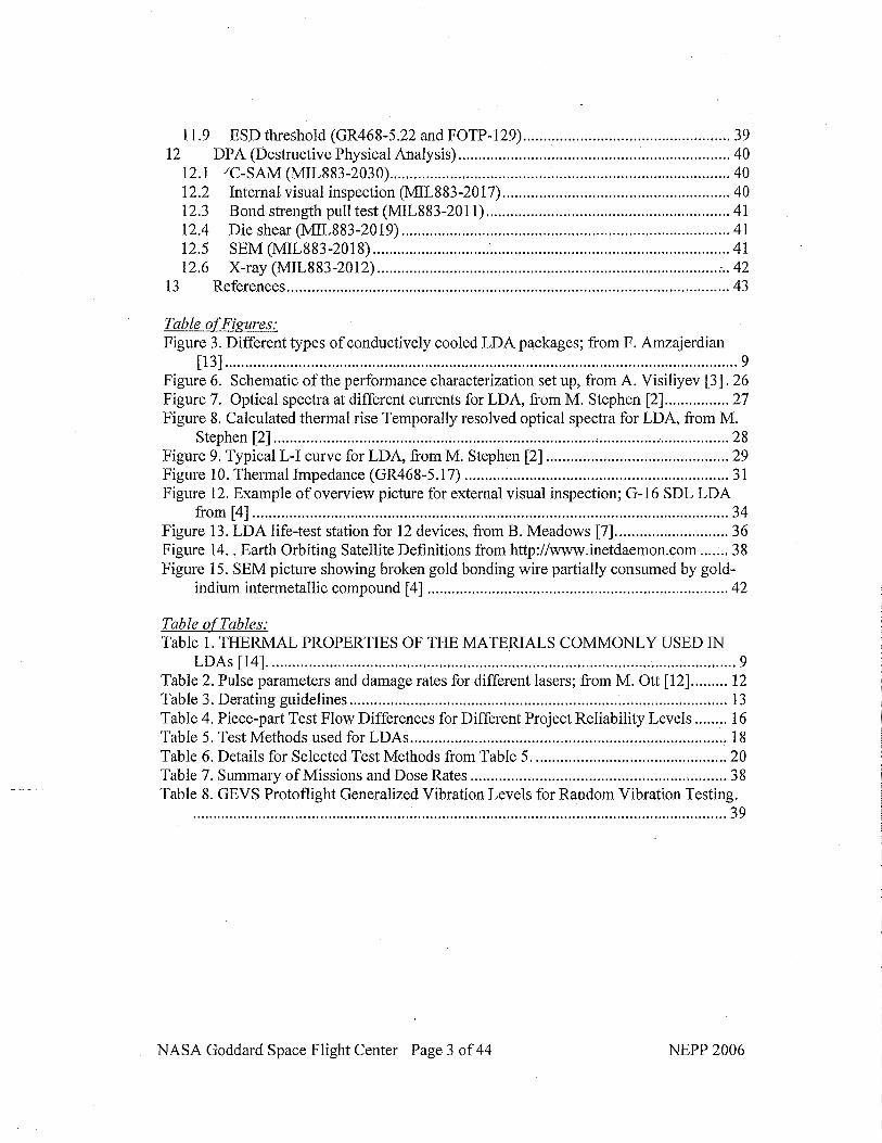
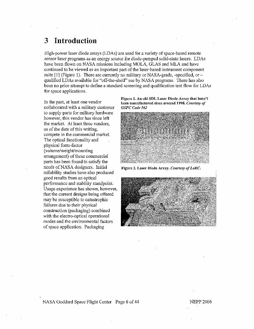
High-power laser diode arrays (LDAs) are used for a variety of space-based remote sensor laser programs as an energy source for diode-pumped solid-state lasers. LDAs have been flown on NASA missions including MOLA, GLAS and MLA and have continued to be viewed as an important part of the laser-based instrument component suite [I] (Figure 1). There are currently no military or NASA-grade, -specified, or - qualified LDAs available for "off-the-shelf' use by NASA programs. There has also been no prior attempt to define a standard screening and qualification test flow for LDAs for space applications.
Figure 1. An old SDL Laser Diode Array that hasn't In the past, at least one vendor been manufactured since around 1998. Courtesy of collaborated with a military customer GSFC Code 562 to supply parts for military hardware however, this vendor has since left the market. At least three vendors, as of the date of this writing, compete in the commercial market. The optical hnctionality and physical form-factor (volume/weight/mounting arrangement) of these commercial parts has been found to satisfy the needs of NASA designers. Initial Figure 2. Laser Diode Array. Courtesy of LaRC. reliability studies have also produced good results from an optical performance and stability standpoint. Usage experience has shown, howeve that the current designs being offered may be susceptible to catastrophic failures due to their physical construction (packaging) combined with the electro-optical operational modes and the environmental factors of space application. Packaging
NASA Goddard Space Flight Center Page 6 of 44 NEPP 2006
design combined with operational mode was at the root of the failures which have greatly reduced the functionality of the GLAS instrument.
The continued need for LDAs for laser-based science instruments and past catastrophic failures of this part type demand examination of LDAs in a manner which enables NASA to select, buy, validate and apply them in a manner which poses as little risk to the success of the mission as possible. To do this the following questions must be addressed:
a. Are there parts on the market that are form-, fit- and function-suitable for the application need?
b. Are the parts which are deemed to be form-, fit- and function-suitable, rugged enough to withstand the environmental conditions of space (temperature, ionizing radiation, vibration, vacuum, etc.) and still operate within specification?
c. Will the parts be able to last, staying within specification, until the end of the mission? Do we have a method for simulating long use life in a relatively short period of time (accelerated life test) to verify this?
d. Does this part type have an "Achilles heel"? Does part have a particular weakness that, if avoided in the application, will avoid premature failure?
e. Are manufacturing lots homogeneous? Is it correct to assume that all parts in the lot behave like the qualification test samples? How about lot-to-lot homogeneity? Will qualification testing be required on every lot?
f. What types of manufacturing defects, which lead to early- or mid-life failure, are the most likely? Do we have test methods which can be used to remove weak members from a production lot without draining too much useful life out of the approved parts?
As a regular practice, NASA supports ongoing evaluation of device technologies such as LDAs through several avenues of research. As a result, a number of experiments and examinations have been performed in support of their selection and use on prior missions. This type of research and use experience has established a baseline for performance and for our understanding of the supply chain, component design and construction, operational capability, ruggedness, reliability, primary failure modes and applicable test methods. From this experience we are able to provide this guideline for use by projects who must verify that the LDAs they are considering for use in flight hardware meet a minimum standard of performance, stability, ruggedness and longevity, and so can be expected to work successfully for the duration of the space mission.
Design of a qualification and screening flow will depend greatly on the mission requirements, the part itself, and the acceptable risks to the project. Cost factors such as the number of parts purchased for destructive tests (destruct samples), fixturing and automated test equipment programming (as applicable) will also greatly influence the test plan. This guideline assumes that the LDAs being evaluated are homogeneous within the purchased lot. That is, each part in the lot has been made with the same materials, on the same manufacturing line, and within the same production period. If this is not the case, it may be very difficult to construct a valid qualification program and the authors of this document (or other qualified personnel), the reliability specialist and the project
NASA Goddard Space Flight Center Page 7 of 44 NEPP 2006
engineers will need to determine how to proceed. It is extremely important then that single lot date code and traceability to common material lots and manufacturing run dates is stated in the contract or purchase order to avoid a lack of intra-lot homogeneity. This applies to rework as well (The SDL LDAs that failed on GLAS had all been reworked to replace one or more bars either to overcome failures or to improve performance.). LDAs at the time of this writing are commercial parts; therefore, there is no guarantee of lot-to-lot homogeneity. Qualification and screening testing is therefore required on every lot. Departures from the recommended tests herein may be deemed necessary on a case-by-case basis and may be due to project risk, cost, schedule or technology factors. It is recommended that users consult the authors or other qualified personnel when re-designing screening and qualification tests for LDAs in order that the effectiveness of those new tests can be maintained while the additional goals are achieved.
LDA Technology Semiconductor lasers diodes emit coherent light by stimulated emission generated inside the cavity formed by the cleaved end facets of a slab of semiconductor. The cavity is typically less than a millimeter in any dimension for single emitters. The diode is pumped by current injection in the p-n junction through metallic contacts. Laser diodes emitting in the range of 0.8 um to 1.06 um have a wide variety of applications including pumping erbium-doped fiber amplifiers, dual-clad fiber lasers, and solid-state lasers used in telecom, aerospace, military, and medical equipment. Direct applications include CD players, laser printers and other consumer and industrial products.
Laser diode bars have many single emitters arranged side-by-side and spaced approximately 0.5 mm apart, on a single slab of semiconductor material measuring approximately 0.5 mm x 10 mm in size. The individual emitters are connected in parallel which keeps the required voltage low at -2V but increases the required current to -50 M a r to 100 Albar. Stacking these laser diode bars 2 to 20+ slabs high yields high power laser diode arrays (LDA's) capable of emitting several hundreds of Watts. Electrically, the bars are wired in series increasing the voltage by 2 Vhar while maintaining the total current at -50 A to 100 A. These arrays are one of the enabling technologies for efficient,
. high power solid-state lasers.
Traditionally these arrays are operated in QCW (Quasi Continuous Wave) mode with pulse widths of -50 ps to 200 ps and repetition rates of -10 Hz to 200 Hz. In QCW mode, the wavelength and the output power of the laser reaches steady-state but the temperature does not. The advantage is a substantially higher output power than in CW mode, where the output power would be limited by the internal heating and the heat sinking properties of the device. The disadvantage is a much higher thermally induced mechanical stress caused by the constant heating and cooling cycle of the QCW operational mode.
The constituent parts and materials of a typical LDA are the diode die (laser bar) and the packaging materials. The packaging design and materials enable the array of laser bars to
NASA Goddard Space Flight Center Page 8 of 44 NEPP 2006
stay together in a stack, to be energized electrically (with a relatively high drive current), to pass the heat generated out of the unit to the mounting surface (thermal path, heat sinking), to be sufficiently rugged against mechanical insults, to provide a standard mounting interface (screws or clamps) and to be as small as possible.
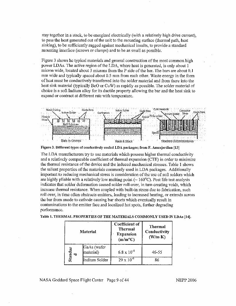
Figure 3 shows he typical materials and general construction of the most common high power LDAs. The active region of the LDA, where heat is generated, is only about 1 micron wide, located about 3 microns fiom the P side of the bar. The bars are about 0.1 mm wide and typically spaced about 0.5 mm from each other. Waste energy in the form of heat must be conductively transferred into the solder material and from there into the heat sink material (typically Be0 or CuW) as rapidly as possible. The solder material of choice is a soft Indium alloy for its ductile property allowing the bar and the heat sink to expand or contract at different rate with temperature.
Figure 3. Different types of conductively cooled LDA packages; from F. Amzajerdian [13]
The LDA manufacturers try to use materials which possess higher thermal conductivity and a relatively comparable coefficient of thermal expansion (CTE) in order to minimize the thermal resistance of the device and the induced mechanical stresses. Table 1 shows the salient properties of the materials commonly used in LDA packages. Additionally important to reducing mechanical stress is consideration of the use of soft solders which are highly pliable with a relatively low melting point (- 160°C). Post life test analysis indicates that solder deformation caused solder roll-over, in turn creating voids, which increase thermal resistance. When coupled with built-in stress due to fabrication, such roll over, in time often obstructs emitters, leading to increased heating, or extends across the bar fiom anode to cathode causing bar shorts which eventually result in contaminations to the emitter face and localized hot spots, hrther degrading performance.
Table 1. THERMAL PROPERTIES OF THE MATERIALS COMMONLY USED IN LDAs [14].
NASA Goddard Space Flight Center Page 9 of 44 NEPP 2006
. Excessive heating and thermal cycling of the LDA active regions plays a key role in limiting the reliability and lifetime of LDAs operated in the QCW mode, particularly where pulse widths are long. To improve the assembly's heat extraction performance, advanced materials are being considered for packaging LDAs, which have high thermal conductivity and a CTE (Coefficient of Thermal Expansion) that matches that of the laser bars. Prior packaging designs used by NASA have used more well-known materials and configurations to achieve these goals (Figure 2). These include:
a. gold wire bonds b. varieties of eutectic solders within a single unit (to enable sequential
construction steps without reflowing prior solder bonds or joints) c. high thermal conductivity materials used for substrates and end clamps such
as ceramic (Alumina, BeO), copper-tungsten (CuW) and copper. d. thick film gold patterning e. gold plating over electrodeless nickel plating f. threaded mounting holes
Future materials may include CVD diamond, matrix metal composites, and carbon- carbon composite graphite foam [14].
LDAs are typically a component within a laser subsystem. It is not encapsulated but rather protected at the box level with the other laser components. The laser system box is normally hermetically sealed and evacuated, or the box can be backfilled with nitrogen or some other inert gas. A thermoelectric cooler (TEC) may or may not be required depending on the thermal design of the LDA and the box. The choice of LDA may drive the use of a TEC, which in turn reduced the overall reliability of the laser system by introducing additional components.
5 Physics of LDA Failure Modes and LDA Reliability
Experiments, qualification testing and usage of LDAs to date by NASA have revealed some strengths and weaknesses for space flight applications. Failure and aging modes and mechanisms associated with LDAs are both related to their constituent parts and materials and how the finished item is applied. Some of these behaviors and defects are generic to microcircuit, transistorand diode parts and some are more unique to LDAs because of the specific way LDAs are assembled and operated. Inadvertent overstress is not normally considered in an analysis of time-to-failure, though it is important to note that a reliability analysis may result in redefining safe operating conditions to ensure the desired lifetime of the part.
NASA Goddard Space Flight Center Page 10 of 44 NEPP 2006
The primary Catastrophic Optical Damage (COD) is certainly the most obvious (or observable) failure mechanism of high power laser diodes to the semiconductor facet, but not the primary cause. A thermal runaway caused by absorption of laser light at the laser facet, and subsequent heating of the facet, causes COD. Temperature rises of several hundred degrees can occur, which causes the facet to melt and a cessation of operation. This and other degradation mechanisms affect both the output power and the emission spectra of the device. Stress induced by the mounting process and the increased thermal impedance can cause a significant change in the center wavelength and a broadening of the spectral width, both on the order of Inm. In addition, the shape of the emission spectrum changes significantly. The following are additional failure mechanisms that have been discovered with use of this type of device:
Bond wire failure Solder creeplmigration ' Solder de-bonding Laser bar material defects Cracking of semiconductor from wedge bonds Gradual aging manifested by decreasing light output and increased current to maintain operation at a specified output Operation at excessive temperature Electrical overstress due to an ESD event Transient current pulses during operation.
* Thermal induced (overheating)
5. I Failures of the past Prior to 2004 the LDAs obtained for the CALIPSO mission (part number SDL-32-00881 made by Spectra Devices Laboratory) were failing due to broken internal connections and shorts (the LDAs were made by the same vendor who had supplied LDAs for MOLA, GLAS and MLA). During failure analysis the parts were found to have several critical defects with root causes in the packaging material selection and construction methods combined with the thermal cycling behavior the LDAs create internally when they are used in the QCW mode. See Code 562 failure analysis report Q30275EV, the Laser Reliability Website: http://nepp.nasa.gov/index~nasa.c~1133/, and the Wirebond website: htt~:llne~p.nasa.aov/wirebond/laser diode arrays.htm for explanations and background for this failure [5]. In-flight failure of the GLAS instrument is strongly believed to be rooted in the failure of the LDAs due to the mechanisms discovered in the CALIPSO parts.
Specifically the failures were both caused by extensive flow and creep of indium solder. In one area it was due to insufficient heat sinking and in the other due to mechanical stress due to over-torqued mounting hardware. In the first case the indium came in direct and extensive contact with the gold wire bonds leading to a severe degradation of those wire bonds due to intermetallic formation between the indium and gold consuming the majority of the wire bond, increasing the current density in the connection and reducing the wire bond's strength. The brittle intermetallics eventually fractured due to fatigue afier a number of thermal excursions. Afier fracture of a given wire, the
NASA Goddard Space Flight Center Page 11 of 44 NEPP 2006
remaining wires conducted more current, thereby accelerating the thermal excursions. When enough wires fractured, the remaining ones melted; the last ones vaporized. During gold wire vaporization, a multi-amp current resulted which caused the diode bar to fail. Since the laser diode bars in the array are connected in series, the destruction of one laser diode bar resulted in an inoperable LDA. In the second case the indium solder was extruded out of place and into a mounting hole causing an electrical short when the mounting screw was over-torqued.
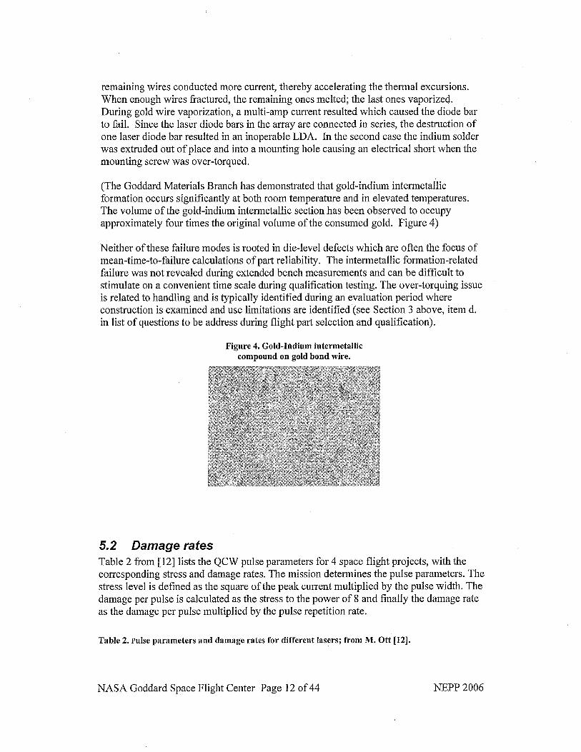
(The Goddard Materials Branch has demonstrated that gold-indium intermetallic formation occurs significantly at both room temperature and in elevated temperatures. The volume of the gold-indium intermetallic section has been observed to occupy approximately four times the original volume of the consumed gold. Figure 4)
Neither of these failure modes is rooted in die-level defects which are often the focus of mean-time-to-failure calculations of part reliability. The intermetallic formation-related failure was not revealed during extended bench measurements and can be difficult to stimulate on a convenient time scale during qualification testing. The over-torquing issue is related to handling and is typically identified during an evaluation period where construction is examined and use limitations are identified (see Section 3 above, item d. in list of questions to be address during flight part selection and qualification).
Figure 4. Gold-Indium intermetallic compound on gold bond wire.
5.2 Damage rates Table 2 from [12] lists the QCW pulse parameters for 4 space flight projects, with the corresponding stress and damage rates. The mission determines the pulse parameters. The stress level is defined as the square of the peak current multiplied by the pulse width. The damage per pulse is calculated as the stress to the power of 8 and finally the damage rate as the damage per pulse multiplied by the pulse repetition rate.
Table 2. Pulse parameters and damage rates for different lasers; from M. Ott [12].
NASA Goddard Space Flight Center Page 12 of 44 NEPP 2006
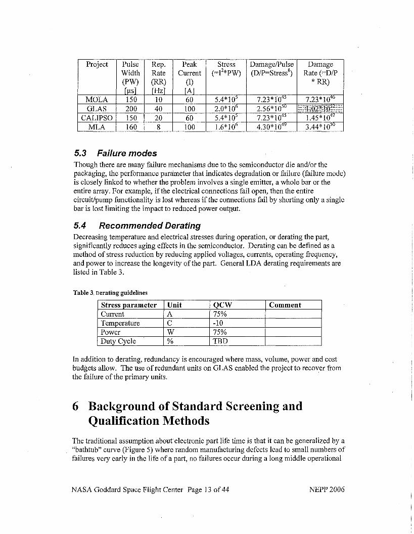
5.3 Failure modes Though there are many failure mechanisms due to the semiconductor die and/or the packaging, the performance parameter that indicates degradation or failure (failure mode) is closely linked to whether the problem involves a single emitter, a whole bar or the entire array. For example, if the electrical connections fail open, then the entire circuit/pump functionality is lost whereas if the connections fail by shorting only a single bar is lost limiting the impact to reduced power output.
Damage Rate (=DR
* RR)
7.23" 1 046 p- 1.02" 1 052
1.45*10~~ 3.44" los0
Project
MOLA GLAS
CALIPSO MLA
5.4 Recommended Derating Decreasing temperature and electrical stresses during operation, or derating the part, significantly reduces aging effects in the semiconductor. Derating can be defined as a method of stress reduction by reducing applied voltages, currents, operating frequency, and power to increase the longevity of the part. General LDA derating requirements are listed in Table 3.
Table 3. Derating guidelines
Comment Current 75%
Power 75% % TBD
DamageRulse (~/P=~tress ' )
7.23 * 2.56" lo5' 7.23* lo4' 4.30" lo4'
Pulse Width ( P W [ps] 150 200 150 160
In addition to derating, redundancy is encouraged where mass, volume, power and cost budgets allow. The use of redundant units on GLAS enabled the project to recover from the failure of the primary units.
6 Background of Standard Screening and Qualification Methods
Rep. Rate W)
10 40 20 8
The traditional assumption about electronic part life time is that it can be generalized by a "bathtub" curve (Figure 5) where random manufacturing defects lead to small numbers of failures very early in the life of a part, no failures occur during a long middle operational
NASA Goddard Space Flight Center Page 13 of 44 NEPP 2006
Peak Current
(1) [A] 60 100 60 100
Stress (=I~*Pw)
5.4*105 2.0*106 5.4*105 1.6*106
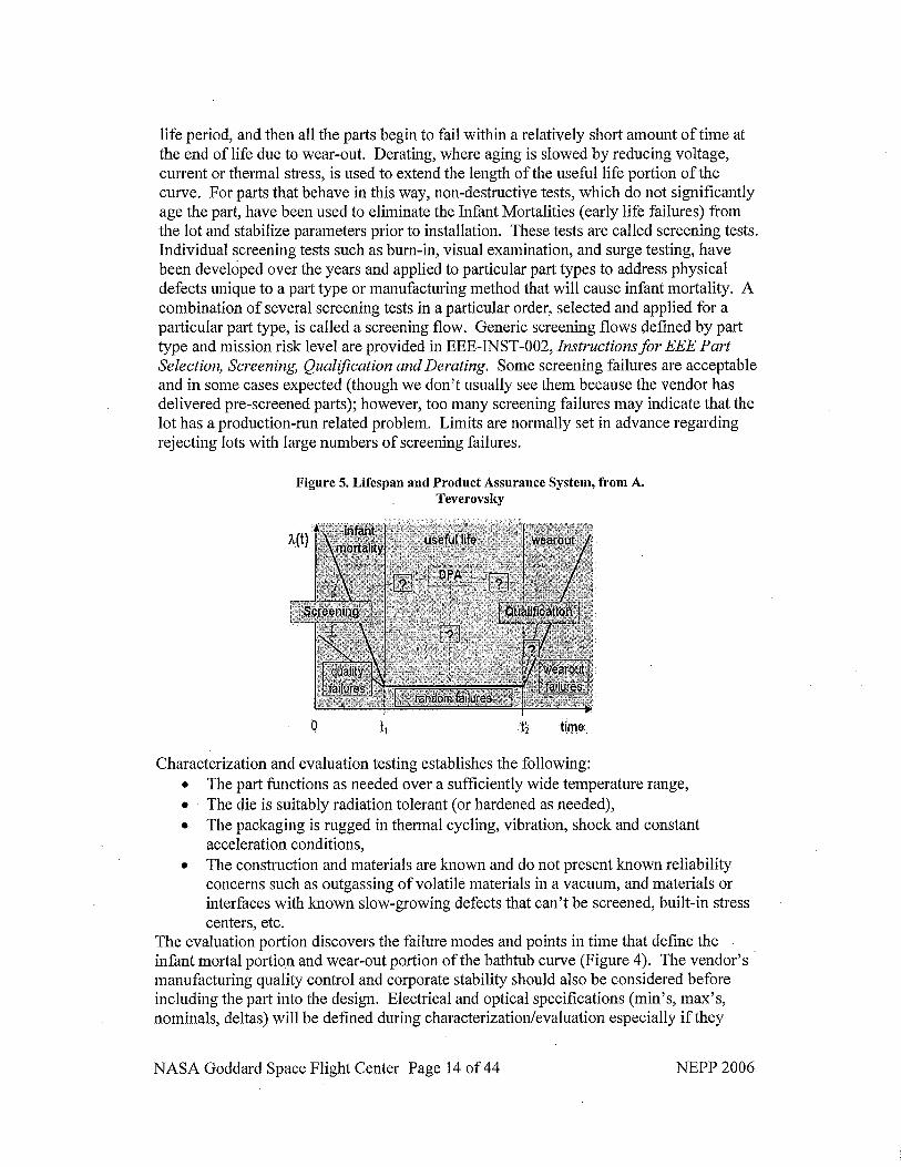
life period, and then all the parts begin to fail within a relatively short amount of time at the end of life due to wear-out. Derating, where aging is slowed by reducing voltage, current or thermal stress, is used to extend the length of the useful life portion of the curve. For parts that behave in this way, non-destructive tests, which do not significantly age the part, have been used to eliminate the Infant Mortalities (early life failures) fiom the lot and stabilize parameters prior to installation. These tests are called screening tests. Individual screening tests such as burn-in, visual examination, and surge testing, have been developed over the years and applied to particular part types to address physical defects unique to a part type or manufacturing method that will cause infant mortality. A combination of several screening tests in a particular order, selected and applied for a particular part type, is called a screening flow. Generic screening flows defined by part type and mission risk level are provided in EEE-INST-002, Instructions for EEE Part Selection, Screening, QualiJication and Derating. Some screening failures are acceptable and in some cases expected (though we don't usually see them because the vendor has delivered pre-screened parts); however, too many screening failures may indicate that the lot has a production-run related problem. Limits are normally set in advance regarding rejecting lots with large numbers of screening failures.
Figure 5. Lifespan and Product Assurance System, from A. Teverovsky
0 t, time
Characterization and evaluation testing establishes the following: The part functions as needed over a sufficiently wide temperature range, The die is suitably radiation tolerant (or hardened as needed), The packaging is rugged in thermal cycling, vibration, shock and constant acceleration conditions, The construction and materials are known and do not present known reliability concerns such as outgassing of volatile materials in a vacuum, and materials or interfaces with known slow-growing defects that can't be screened, built-in stress centers, etc.
The evaluation portion discovers the failure modes and points in time that define the infant mortal portion and wear-out portion of the bathtub curve (Figure 4). The vendor's manufacturing quality control and corporate stability should also be considered before including the part into the design. Electrical and optical specifications (min's, max's, nominals, deltas) will be defined during characterization/evaluation especially if they
NASA Goddard Space Flight Center Page 14 of 44 NEPP 2006
differ from the manufacturer's datasheet;-GEVS-STD-7000, General Environmental Verification Standard for GSFC Flight Programs and Projects describes environmental conditions to consider when running evaluation tests (also see: "Environmental Conditions for Space Hardware: A Sztwey" at http:!/~~epp.nasa.aov/index nasa.cfin/486/CSE0869C-O469-4Dl I- 9FAA8012C8F52351/ for an overview). If the project cannot afford the time and cost of extensive characterization and evaluation testing, it might decide to accept the risk of flight lot failure by waiting to do some of these examinations during qualification testing. This is regrettably the norm at the time of this writing, because all of the currently available products are considered commercial grade and lack lot-to-lot homogeneity.
Qualification testing accomplishes both a validation of the ruggedness testing done during characterization/evaluation and validates that the life expectancy is sufficient. Acceptlreject criteria are defmed using the electrical and optical specifications established during characterization. The ruggedness portion will include exposure to extreme temperatures, humidity, thermal cycling andlor thermal shock, vibration and other mechanical, thermal or electrical stresses, establishing that the part lot in hand can persevere in the'application. The mission requirements, expected handling and other pre- launch conditions define the limits of the stresses. Reliability testing uses a set of conditions intended to simulate aging as the part would in the application (including how it would age for the electrical or optical mode in which it is used). Stress conditions are heightened in an effort to accelerate the aging process, thereby reducing test time. This is called life testing. For mature, well understood part types, such as bipolar and CMOS semiconductor devices, film resistors, ceramic and tantalum capacitors, the Arrhenius equation can be used to calculate the test time combined with temperature and voltage or current needed to simulate long test times. For parts which do not have a reliability model based on the Arrhenius equation, we tend to use this same approach until a non- correlating behavior has been established which leads to a different model.
Qualification testing is normally performed on screened units so as not to bias the statistics of the results with failures that would have normally been removed from the lot prior to part installation. Sample sizes used for the reliability testing are traditionally defined by MIL-STD-690, Failure Rate Sampling Plans and Procedures, and are based on confidence level. For part types that can be very expensive at the piece part level, such as LDAs, statistical analysis resulting in a projected failure rate (or mean time to failure) may not be feasible. For these part types, life test sample sizes are determined in accordance with the needs and limitations of the project. Samples are allocated among the one or multiple branches of the overall test flow. The arrangement of the tests in the test flow branches are designed to both maximize the reuse of the samples and to simulate the sequence of stresses that the part will actually experience, without creating an unrealistic overly stressful scenario.
DPA is used during lot acceptance/approval to verify that the part is constructed as expected and does not have defects that can be assumed to affect the remainder of the lot. The sample size is typically one or two pieces. Wire bond pull is often done as part of DPA to check that the bond strength meets minimum standards and that the all the bonds are "in family" indicating a consistent bonding process. Excessive amounts of intermetallic material around the bond on the bond pad (coming from underneath the
NASA Goddard Space Flight Center Page 15 of 44 NEPP 2006
bond) can indicate that contamination was not removed prior to bonding or that contamination has diffused into the bond. Contamination in wire bonds can lead to bond lifts (cracks extending across the entire bond joint) with time and temperature. Standard Internal Visual test methods are used to identify non-compliant physical attributes such as cracked die, loose particles, chemical stains, excessive die attach material, damaged spacing of electrical conductors, etc. prior to delivery of the units. DPA is done after the units have been purchased. Projects may choose to use DPA to analyze samples used in qualification testing in addition to the DPA performed on a screened unit.
7 Availability of Standard Space-Grade Laser Diode Arrays
The Parts, Packaging and Assemblies Technology Branch (Code 562) describes standard screening and qualification test flows for electrical, electronic and photonic parts in the document EEE-INST- 002 in a format which connects project reliability target level to the quality/reliability level of the part selected, and the screening and qualification testing that must be applied. Level 1 part selection and test requirements are the most comprehensive, Level 2's are less rigorous and Level 3's are least rigorous (Table 4).
The standard test flows and the test methods used to form the flows, described for space parts in EEE-INST-002, are modeled after those which have been used by the high reliability electronics community for decades and which are ubiquitous in the military specification system. Parts regularly produced and tested using these flows, whether by virtue of their being military specification parts or via a vendor's standard practice, are considered standard and "off-the-shelf' space-grade parts and do not receive additional testing by NASA prior to installation. Parts that are not processed and tested in accordance with EEE-INST-002, for the project reliability level required, prior to delivery to NASA, must pass those additional tests before they are admitted to flight inventories. It is preferred to require that the vendor demonstrate passing data for all of the testing prior to delivery rather than having the testing done on purchased parts by the user. In this way NASA avoids buying failed lots and has the option to seek another vendor rather than continue the purchase via a lot rebuild.
Table 4. Piece-part Test Flow Differences for Different Project Reliability Levels
NASA Goddard Space Flight Center Page 16 of 44 NEPP 2006
Project requirement 1
2
3
Reliability level HigWproven
Medium
Lowlunknown
Risk level Low
Low-moderate
Highlunknown
Examples of Test Flow Features
Extended hours of burn-in, lowest life test failure rates, internal element
control, DPA, X-Ray Shorter burn-in, higher number of life test failures allowed, no serialization of samples, less mechanical testing
Less screening and no qualification
testing
The lack of long-term use, in relatively high volumes, of LDA's by the military and NASA has retarded the emergence of military and NASA specifications. At this time there do not exist any standard space-grade LDA's. Further, there has not been an opportunity to develop a three-tiered screening and qualification plan that aligns with the three project reliability levels described in EEE-INST-002. This document describes tests that can be used to develop a flow that can be used for all three reliability levels, 1 through 3.
8 Survey of Test Method Usage by Industry and GSPC for Assessing LDAs
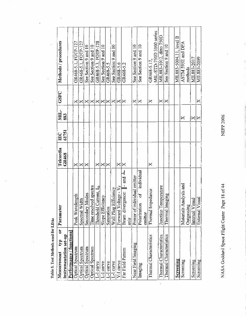
The tests and standard test methods shown in Table 5 have been applied in the past in the commercial sector and by NASA experimenters. This survey showed that there is a baseline of practice in the industry for performing screening, qualification and DPA tests on LDAs and that there can be some expectation that prior data may be available for review or that a vendor has a process for performing these tests on parts prior to shipping (and thus designing parts which will pass the tests). Note: MIL-STD-883 is military standard that contains standard test methods as well as test flows traditionally used for packaged monolithic microcircuit parts. Claims by vendors that their parts are tested to "883" or other references to MIL-STD-883 indicate that a test methods detailed in MIL- STD-883 have been used to verify part performance and/or that the test flow in the "5000 section" of MIL-STD-883 was used. This flow may or may not be comprehensive for a given LDA or application of an LDA.
Table 5 elaborates on some of the test methods listed in Table 6 and indicates data that might be available from prior testing by the vendor. Insights about how to make some of the measurements are hrther detailed in the numbered paragraphs in section 9 below. This type of data can be obtained by the user or may be included in the vendor's datasheet. It is always advantageous to buy parts which have been screened and qualified by the manufacturer. Though this makes the parts more costly (to cover both testing and device fall-out) and drives up lead times, the procurement quantity will not unexpectedly be reduced when parts fail screening or the whole lot fails qualification aRer it has been paid for. Also, vendors who perform space-flow screening and qualification testing tend to use designs and production practices that result in higher yields in general (less parts scrapped) and have a more detailed understanding of the impact of design and manufacturing processes on their part's reliability. They are also more invested in resolving failures.
NASA Goddard Space Flight Center Page 17 of 44
Tab
le 5
. Tes
t Met
hods
use
d fo
r L
DA
s
NA
SA
God
dard
Spa
ce F
ligh
t Cen
ter
Pag
e 18
of 4
4

et7 30 6 T a8vd Jalua3 l@!1d
a3
~d
s PJvPP0-E) VSV
N
-£88?MT 'O
Z'S-89VX
D
LOO
T'900I 'SOOT
8102-£88TtN
z
~o
~-~
88
?IN
6102-E
SSTN
T 102-£887IN
£102-£88?IW
[ O
EOZ-E88TN
0202-£88?IW
[ uo!lquaurm
op u81saa O
L-N
- T T £-S VSV
N
'T'600~-£88?1N
X
X
X
x X
X
X
X
X
X
x x X
X
X
X
X
N8
S
1631-x
JYS
a!a y@
ua~os puoq aJIM
~v
ns
r~
~
vm
alu
~
WS
-3
aN
Id
uo!~v~n8rjuo3 auyasr?a
x
Vd
a
Tdda
vd
a
Vd
a
V~
Q[
Vd
a
vd
a
Vd
a
-1 Vda
JO
8u!1.sX3
amw
v~adtua~
a3umnpuw
Ivluamoqaug
Tab
le 6
. Det
ails
for
Sele
cted
Tes
t Met
hods
from
Tab
le 5
.
Mea
sure
men
t ty
p or
in
stru
men
tati
on s
et-u
p E
nvir
onm
enta
l End
uran
ce
Env
iron
men
tal E
ndur
ance
M
echa
nica
l M
echa
nica
l E
lect
rica
l M
echa
nica
l
NA
SA G
odda
rd S
pace
Flig
ht C
ente
r Pa
ge 2
0 of
44
Par
amet
er
The
rmal
Sho
ck
Rad
iatio
n M
echa
nica
l Sho
ck
Ran
dom
Vib
ratio
n E
SD S
ensi
tivity
R
adio
grap
hy, X
-ray
Tes
t
Per
form
ance
Pe
ak W
avel
engt
h
Spec
tral
Wid
th
Seco
ndar
y M
odes
Tim
e re
solv
ed s
pect
ra
Thr
esho
ld c
urre
nt, I
th
NE
PP 2
006
Tel
cord
ia
GR
468
X
X
X
X
Met
hod
or
Pro
cedu
re
GR
468-
5.1
FOT
P-12
7
GR
468-
5.1
FOT
P-12
7
GR
468
See
[2]
GR
468-
5.3
FOT
P-12
8
IEC
61
751
X
X
X Con
diti
ons
At 2
5"C
, min
& m
ax te
mpe
ratu
re: O
SA re
ad-
out o
f pea
k w
avel
engt
h us
ing
peak
sea
rch;
typ.
-8
08nm
A
t 25"
C, m
in &
max
tem
pera
ture
: OSA
read
of
FWH
M u
sing
bui
lt-in
fun
ctio
n or
mar
kers
; typ
. -3
nm
At 2
5"C
, min
& m
ax te
mpe
ratu
re: O
SA re
ad-
out o
f wav
elen
gths
and
SM
SR u
sing
bui
lt-in
fu
nctio
n or
mar
kers
. U
se O
SA a
s B
P fi
lter,
hig
h-sp
eed
phot
odio
de
& o
scill
osco
pe. S
can
OSA
wav
elen
gth
and
take
inte
nsity
vs.
tim
e, a
nd th
en p
lot p
eak
wav
elen
gth
vs. t
ime.
A
t 25O
C, m
in &
max
tem
pera
ture
: pow
er m
eter
an
d A
mpe
re m
eter
read
-out
; typ
. -10
-20A
MIL
- 88
3 X
X
X
X
X
X
Sect
ion
9.2.
1
9.2.
2
9.2.
3
9.3 0
May
be
in
the
vend
or's
da
tash
eet
X
X
GSF
C
X
X
X
X
X
Met
hods
/ pr
oced
ures
MIL
883-
1011
M
IL88
3-10
19
MIL
883-
2002
M
IL88
3-20
26
GR
468-
5.22
, FO
TP-
129
MIL
883-
2012
NA
SA G
odda
rd S
pace
Flig
ht C
ente
r Pa
ge 2
1 o
f 44
Tes
t
L-I
cur
ve S
lope
L-I
cur
ve s
atur
atio
n, m
ax p
ower
Wal
l plu
g ef
fici
ency
V-I
Cur
ve a
nd V
F at
thre
shol
d
Far F
ield
Pat
tern
, Bea
m
dive
rgen
ce 11 -
and
I-ax
is
.
Nea
r fi
eld
imag
ing,
pow
er o
f in
divi
dual
em
itter
Im
agin
g, P
olar
izat
ion
of
indi
vidu
al e
mitt
ers
The
rmal
impe
danc
e
Junc
tion
Tem
pera
ture
T
herm
al im
agin
g
Scre
enin
g;
Mat
eria
ls A
naly
sis
NE
PP 2
006
Met
hod
or
Pro
cedu
re
GR
468
GR
468-
5.5
GR
468-
5.6
GR
468-
5.2
GR
468-
5.17
Con
diti
ons
At 2
5"C
, min
& m
ax te
mpe
rabr
e: p
ower
met
er
and
Am
pere
met
er re
ad-o
ut; t
yp. -
1 W
/A+
At 2
5"C
, min
& m
ax te
mpe
ratu
re; p
ower
met
er
and
Am
pere
met
er re
ad-o
ut; t
yp. -
50-1
00W
W
all p
lug
effi
cien
cy is
ratio
of
light
out
put
pow
er to
dis
sipa
ted
elec
tric
al p
ower
; typ
.-50%
A
t 25"
C, m
in &
max
tem
pera
ture
; vol
t met
er
and
Am
pere
met
er re
ad-o
ut; t
yp. -
2V
Bea
m d
iver
genc
e an
gles
par
alle
l and
pe
rpen
dicu
lar t
o th
e L
DA
bar
s by
sca
nnin
g a
pow
er d
etec
tor a
cros
s the
far
fiel
d an
d fi
ndin
g th
e FW
HM
. -10
" an
d -4
0°,
resp
ectiv
ely.
N
ear
fiel
d im
ages
usi
ng C
CD
sho
ws
light
in
tens
ity o
f ind
ivid
ual e
mitt
ers.
Po
lari
zatio
n an
alyz
er in
fi-o
nt o
f CC
D s
how
s po
lari
zatio
n st
ate
of in
divi
dual
em
itter
s.
With
the
larg
e am
ount
s of
pow
er d
issi
pate
d (-
50W
) in
the
LD
A's
-2O
C/W
is
requ
ired
.
Use
a 3
-5pm
wav
elen
gth
rang
e in
frar
ed c
amer
a sy
nchr
oniz
ed w
ith th
e L
DA
dri
ve p
ulse
s. L
ook
for h
ot-s
pots
(A
P5"
C)
at in
divi
dual
em
itter
s.
Iden
tify
mat
eria
ls a
nd th
eir
loca
tion
insi
de th
e pa
ckag
e us
ing
eith
er v
endo
r dat
a or
by
DPA
. T
his
prov
ides
relia
bilit
y in
form
atio
n on
the
Sect
ion
9.4.
2
9.4.
3
9.4.
4
9.5.
1
9.6
9.7
9.8 0 9.9
10.1
May
be
in
the
vend
or's
da
tash
eet
X
X
X
X
X
X
NA
SA G
odda
rd S
pace
Flig
ht C
ente
r Pa
ge 2
2 of
44
Tes
t
The
rmal
Vac
uum
Out
gass
ing
NE
PP 2
006
Met
hod
or
Pro
cedu
re
AST
M 5
95E
Con
diti
ons
pack
agin
g co
nfig
urat
ion
as w
ell a
s w
hich
m
ater
ials
are
non
-met
allic
for c
onta
min
atio
n re
late
d co
ncer
ns.
100
to 3
00 m
illig
ram
s of
mat
eria
l, 12
5°C
at
le-6
torr
, 24h
. TM
L<1
.O%
and
tota
l
Sect
ion
10.2
May
be
in
the
vend
or's
da
tash
eet
X
mat
eria
l or w
ire
leng
ths;
con
tam
inat
ion
with
fo
reig
n m
ater
ials
or p
artic
les.
A
t 75X
-150
X lo
ok fo
r die
cra
cks;
met
alliz
atio
n
mon
itori
ng a
t1 O
X. F
ail i
f sep
arat
ion
forc
e is
NA
SA G
odda
rd S
pace
Flig
ht C
ente
r Pa
ge 2
3 of
44
NE
PP 2
006
NA
SA G
odda
rd S
pace
Flig
ht C
ente
r Pa
ge 2
4 of
44
Tes
t
Con
stan
t Acc
eler
atio
n
Acc
eler
ated
Agi
ng
NE
PP 2
006
Met
hod
or
Pro
cedu
re
MIL
883-
2001
.2
GR
468-
5.18
FO
TP-
130
Mec
hani
cal S
hock
Con
diti
ons
Lev
el E
: 30,
00O
G, 1
min
ute/
axis
/dir
ectio
n=6
tota
l. Fa
il if
par
ts m
ove
or p
aram
eter
s ch
ange
. +8
5"C
, rat
ed p
ower
, 200
0hrs
ESD
Thr
esho
ld
Sect
ion
11.1
11.2
GR
468-
5.22
May
&t
be in
th
e ve
ndor
's
data
shee
t
50 - 8
00 H
z, +
6 dB
/ oc
tave
80
0 - 2
000
Hz,
.32
g2 /
Hz
2000
Hz,
.052
g2 /
Hz
Ove
rall
Hz,
20.
0 g,,
Tes
t sha
ll be
con
duct
ed fo
r 3
min
utes
per
test
fo
r thr
ee te
sts
tota
l (on
e pe
r x,
y, a
nd z
axi
s).
HB
M te
stin
g fr
om 1
00V
to 1
5kV
. 10-
90%
11
.9
NA
SA G
odda
rd S
pace
Flig
ht C
ente
r Pa
ge 2
5 of
44
Tes
t
NE
PP 2
006
Met
hod
or
Pro
cedu
re
FOT
P- 1
29
Con
diti
ons
rise
-tim
e of
5-1
5ns w
ith a
dec
ay ti
me
of 1
30-
170n
s. M
inim
um 6
sam
ples
to te
st 3
eac
h po
sitiv
e-ne
gativ
e po
lari
ty. A
ll co
mbi
natio
ns o
f tw
o pi
ns w
ith re
mai
ning
pin
s N
C. P
ass
crite
ria
<50%
Ith i
ncre
ase,
40
0%
reve
rse
bias
leak
age
curr
ent r
ise.
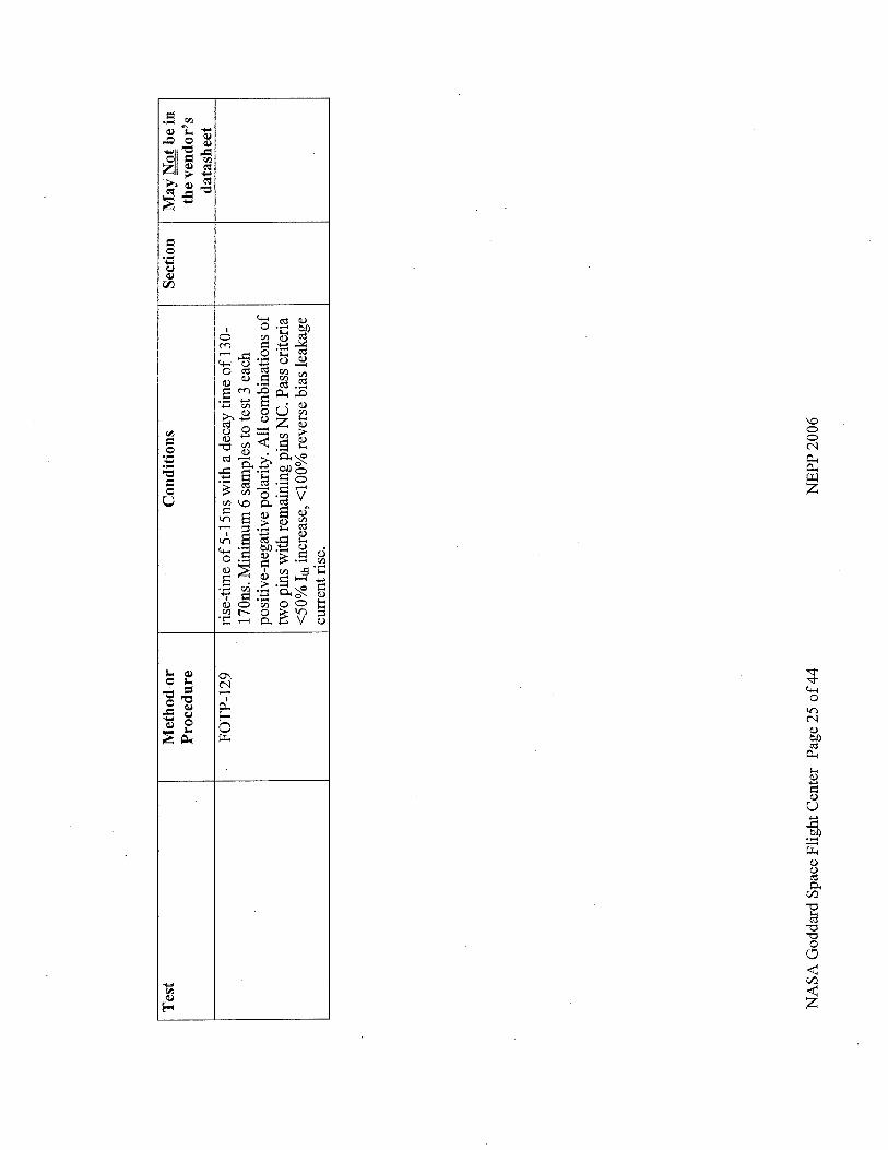
Sect
ion
May
Not
be
in
the
vend
or's
da
tash
eet
9 Performance characterization
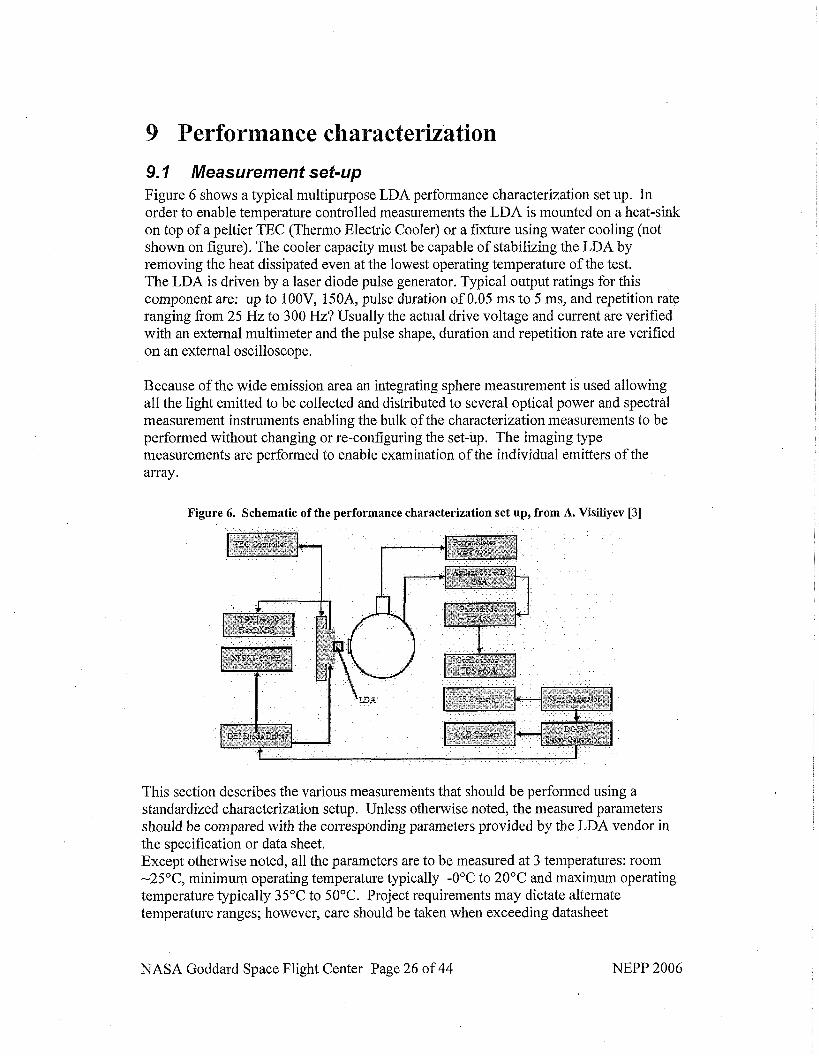
9.1 Measurement set-up Figure 6 shows a typical multipurpose LDA performance characterization set up. In order to enable temperature controlled measurements the LDA is mounted on a heat-sink on top of a peltier TEC (Thermo Electric Cooler) or a fixture using water cooling (not shown on figure). The cooler capacity must be capable of stabilizing the LDA by removing the heat dissipated even at the lowest operating temperature of the test. The LDA is driven by a laser diode pulse generator. Typical output ratings for this component are: up to 100V, 150A, pulse duration of 0.05 ms to 5 ms, and repetition rate ranging from 25 Hz to 300 Hz? Usually the actual drive voltage and current are verified with an external multimeter and the pulse shape, duration and repetition rate are verified on an external oscilloscope.
Because of the wide emission area an integrating sphere measurement is used allowing all the light emitted to be collected and distributed to several optical power and spectral measurement instruments enabling the bulk of the characterization measurements to be performed without changing or re-configuring the set-up. The imaging type measurements are performed to enable examination of the individual emitters of the array.
Figure 6. Schematic of the performance characterization set up, from A. Visiliyev [3]
This section describes the various measurements that should be performed using a standardized characterization setup. Unless otherwise noted, the measured parameters should be compared with the corresponding parameters provided by the LDA vendor in the specification or data sheet. Except otherwise noted, all the parameters are to be measured at 3 temperatures: room -25"C, minimum operating temperature typically -0°C to 20°C and maximum operating temperature typically 35°C to 50°C. Project requirements may dictate alternate temperature ranges; however, care should be taken when exceeding datasheet
NASA Goddard Space Flight Center Page 26 of 44 NEPP 2006
specifications and limits to avoid part overstress. Long-term performance of parts outside of their specification limits should be demonstrated during an evaluation experiment to reduce the risk of failing qualification.
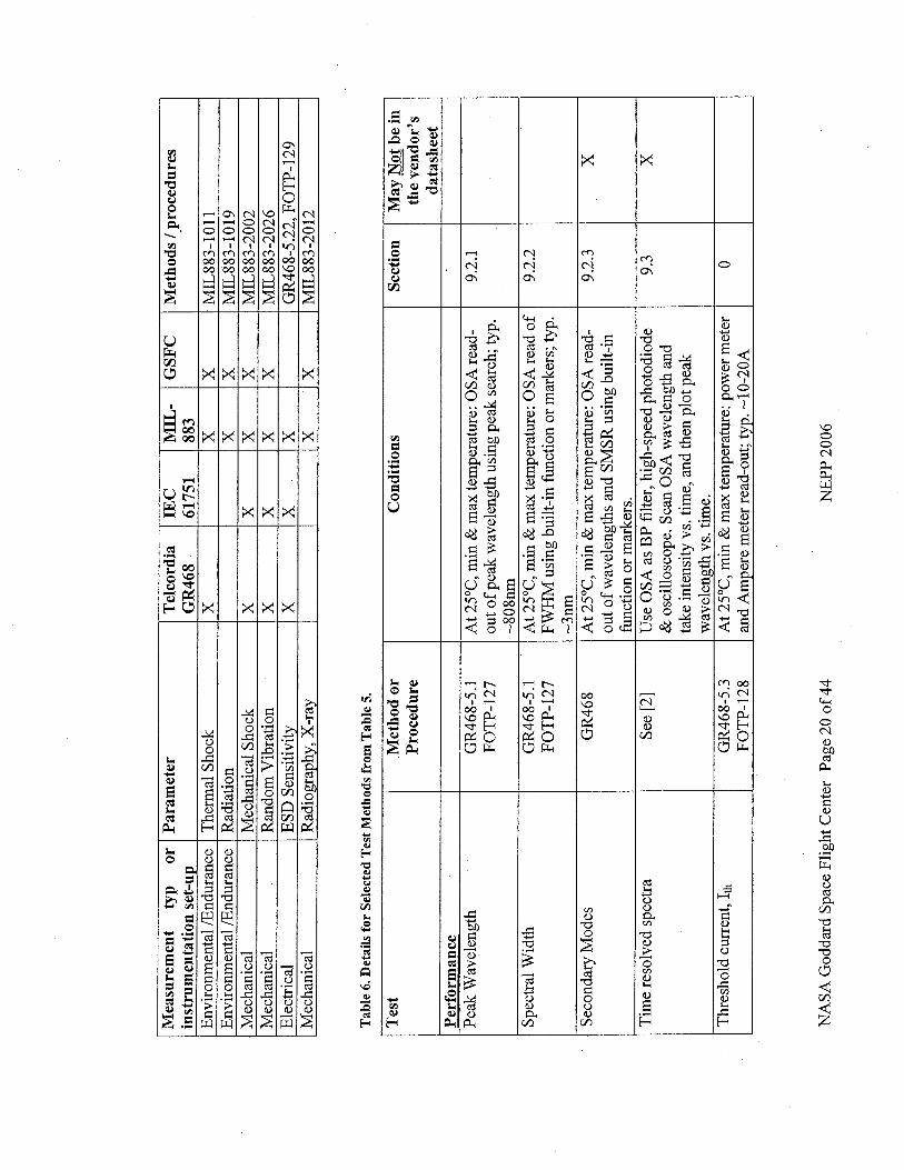
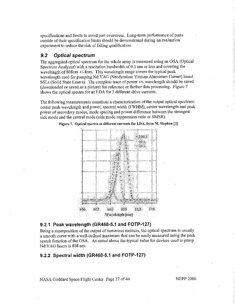
9.2 Opticalspectrum The aggregated optical spectrum for the whole array is measured using an OSA (Optical Spectrum Analyzer) with a resolution bandwidth of 0.1 nm or less and covering the wavelength of 808nm +I-4nm. This wavelength range covers the typical peak wavelength used for pumping Nd:YAG (Neodymium Yttrium Aluminum Garnet) based SSLs (Solid State Lasers). The complete trace of power vs. wavelength should be saved (downloaded or saved as a picture) for reference or further data processing. Figure 7 shows the optical spectra for an LDA for 3 different drive currents.
The following measurements constitute a characterization of the output optical spectrum: center peak wavelength and power, spectral width (FWHM), center wavelength and peak power of secondary modes, mode spacing and power difference between the strongest side mode and the central mode (side mode suppression ratio or SMSR).
Figure 7. Optical spectra at different currents for LDA, from M. Stephen [2]
9.2.1 Peak wavelength (GR468-5.1 and FOTP-127) Being a superposition of the output of numerous emitters, the optical spectrum is usually a smooth curve with a well-defined maximum that can be easily measured using the peak search function of the OSA. As stated above the typical value for devices used to pump Nd:YAG lasers is 808 nrn.
9.2.2 Spectral width (GR468-5.1 and FOTP-127)
NASA Goddard Space Flight Center Page 27 of 44 NEPP 2006
The FWHM value can be obtained for the smooth spectrum curve with a well-defined maximum either using markers or a built-in spectral width function. Typically a value of 2-4 nm is observed. When secondary peaks are observed a more thorough data analysis is required to establish a reliable value for the spectral width.
9.2.3 Secondary modes When secondary peaks are observed the image should be recorded. The center wavelength of the side modes, the power at the side-mode peak, and the mode-spacing (spectral separation of the side-mode peak from the center peak) should be recorded. The SMSR (Side Mode Suppression Ratio) is calculated in dB and is the delta of the power of the center peak and the strongest side-mode peak.
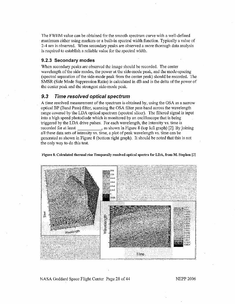
9.3 Time resolved optical spectrum A time resolved measurement of the spectrum is obtained by, using the OSA as a narrow optical BP (Band Pass) filter, scanning the OSA filter pass band across the wavelength range covered by the LDA optical spectrum (spectral slicer). The filtered signal is input into a high speed photodiode which is monitored by an oscilloscope that is being triggered by the LDA drive pulses. For each wavelength, the intensity vs. time is recorded for at least , as shown in Figure 8 (top lee graph) [2]. By joining all these data sets of intensity vs. time, a plot of peak wavelength vs. time can be generated as shown in Figure 8 (bottom right graph). It should be noted that this is not the only way to do this test.
Figure 8. Calculated thermal rise Temporally resolved optical spectra for LDA, from M. Stephen [2]
NASA Goddard Space Flight Center Page 28 of 44 NEPP 2006
The peak wavelength change (in the positive direction) with time is directly related to the heating generated by the drive current pulse fiom which the thermal stress can be assessed. Using the peak wavelength shift recorded in section 9.3, calculate the thermal rise of the LDA using the typical wavelength shift value of -0.27nmPC [3]. However it has been found that this value is not constant, and varies between different diode manufacturers (probably foundries).
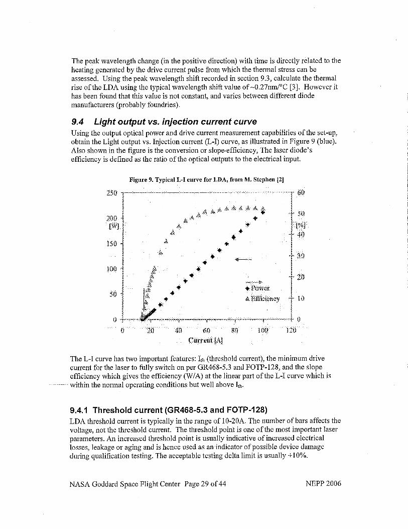
9.4 Lighf oufpuf vs, injecfion currenf curve Using the output optical power and drive current measurement capabilities of the set-up, obtain the Light output vs. Injection current (L-I) curve, as illustrated in Figure 9 (blue). Also shown in the figure is the conversion or slope-efficiency, The laser diode's efficiency is defined as the ratio of the optical outputs to the electrical input.
Figure 9. Typical L-I curve for LDA, from M. Stephen [2]
The L-I curve has two important features: Ith (threshold current), the minimum drive current for the laser to hl ly switch on per GR468-5.3 and FOTP-128, and the slope efficiency which gives the efficiency (WIA) at the linear part of the L-I curve which is within the normal operating conditions but well above Ith.
9.4.1 Threshold current (GR468-5.3 and FOTP-128) LDA threshold current is typically in the range of 10-20A. The number of bars affects the voltage, not the threshold current. The threshold point is one of the most important laser parameters. An increased threshold point is usually indicative of increased electrical losses, leakage or aging and is hence used as an indicator of possible device damage during qualification testing. The acceptable testing delta limit is usually +lo%.
NASA Goddard Space Flight Center Page 29 of 44 NEPP 2006
9.4.2 Slope efficiency A typical number for slope efficiency is -1 W/A or slightly higher. For high power arrays, its closer to 7. The problem with this type of measurement is that a multi-array unit will have the higher slope efficiency, since the current input is the same. It's the voltage that increases. This is also one of the most hndamental laser parameters. It indicates how many Watts of optical power you will get per Ampere injected into the laser in its linear regime, before it starts to roll-over at high currents.
9.4.3 L-l curve saturation, maximum power out (GR468-5.5) At high currents the L-I curve can start to "roll-over" or flatten demonstrating the maximum output power. The slope efficiency will begin to decrease at this point. Typically the maximum output power is specified as powerhar and is on the order of 50- 100Whar.
9.4.4 Wall-plug efficiency The wall plug efficiency directly tells how much of the electrical power dissipated by the LDA is emitted as light. Since light emission only really starts above the threshold, the wall-plug efficiency stays at zero below the threshold and then sharply rises to its fmal, settled value which is typically -50%, when the light output is at its maximum. Figure 9 illustrates a typical wall-plug efficiency curve shown by the pink triangle markers.
9.5 V-I curve (GR468-5.6) Using the LDA voltage and drive current measurement capabilities, the V-I curve is obtained. Usually only the positive V-I values are measured, but extended measurements into the negative range can give important information about leakage currents in the semiconductor.
9.5.1 Forward voltage at threshold (GR468-5.6) The forward voltage at threshold is measured according to GR468-5.6 and typically measures less than 2Vhar.
9.6 Far field (GR468-5.2) The far field measurements are used to characterize divergence angles of the aggregate beam parallel and perpendicular to the LDA bars. This is done by scanning a power detector across the far field in the two directions and finding the FWHM values. Typical values are -10" and -40" for the two directions. These are often referred to as the beam divergence angles for 1) - and Laxis.
9.7 Near field images - emitter power Near field images of the entire array are obtained using a CCD camera with a ND filter These measurements show spatially resolved individual emitter light intensity, which can pinpoint troubled emitters at an early stage.
9.8 Near field images - polarization
NASA Goddard Space Flight Center Page 3 0 of 44 NEPP 2006
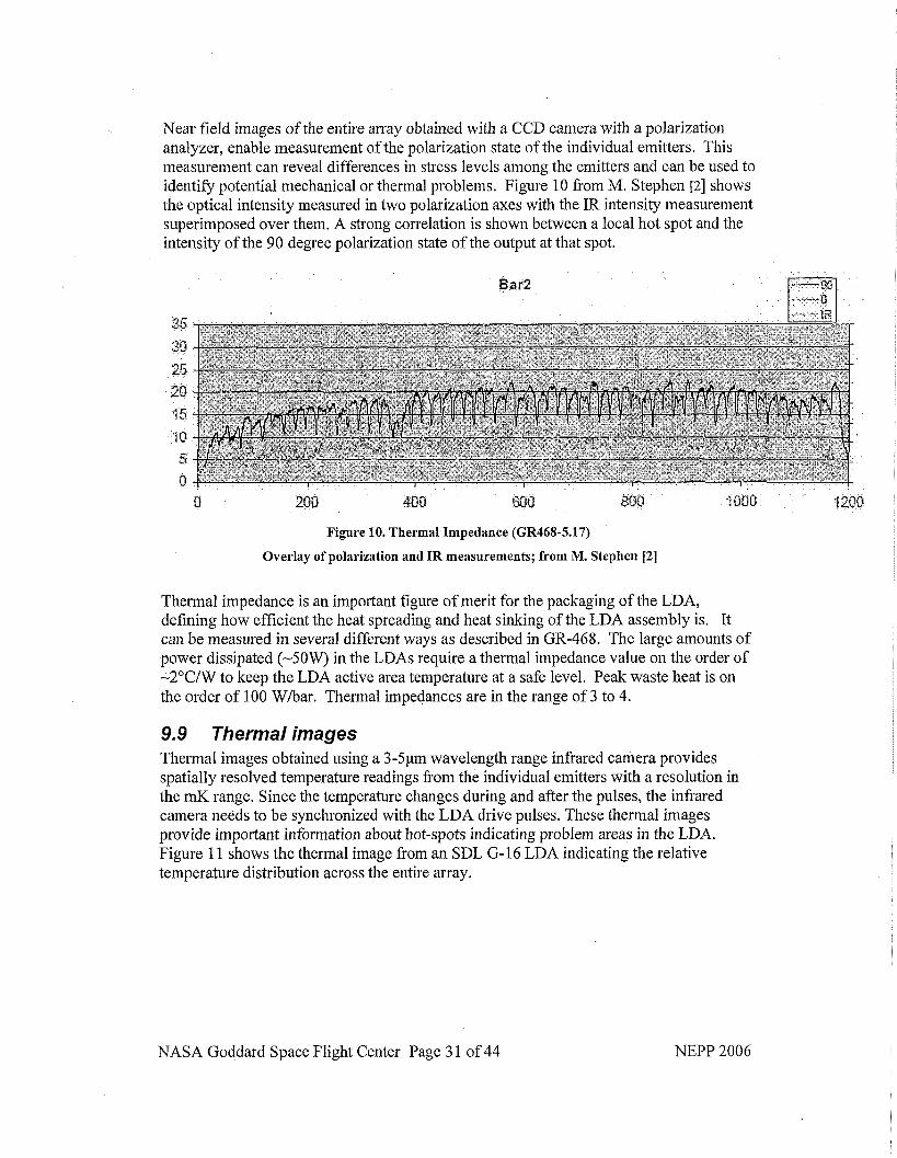
Near field images of the entire array obtained with a CCD camera with a polarization analyzer, enable measurement of the polarization state of the individual emitters. This measurement can reveal differences in stress levels among the emitters and can be used to identify potential mechanical or thermal problems. Figure 10 from M. Stephen [2] shows the optical intensity measured in two polarization axes with the IR intensity measurement superimposed over them. A strong correlation is shown between a local hot spot and the intensity of the 90 degree polarization state of the output at that spot.
Figure 10. Thermal Impedance (GR468-5.17)
Overlay of polarization and IR measurements; from M. Stephen [Z]
Thermal impedance is an important figure of merit for the packaging of the LDA, defining how efficient the heat spreading and heat sinking of the LDA assembly is. It can be measured in several different ways as described in GR-468. The large amounts of power dissipated (-50W) in the LDAs require a thermal impedance value on the order of -2"CIW to keep the LDA active area temperature at a safe level. Peak waste heat is on the order of 100 Wlbar. Thermal impedances are in the range of 3 to 4.
9.9 Thermal images Thermal images obtained using a 3-5pm wavelength range infrared camera provides spatially resolved temperature readings from the individual emitters with a resolution in the rnK range. Since the temperature changes during and after the pulses, the infrared camera needs to be synchronized with the LDA drive pulses. These thermal images provide important information about hot-spots indicating problem areas in the LDA. Figure 11 shows the thermal image from an SDL G-16 LDA indicating the relative temperature distribution across the entire array.
NASA Goddard Space Flight Center Page 3 1 of 44
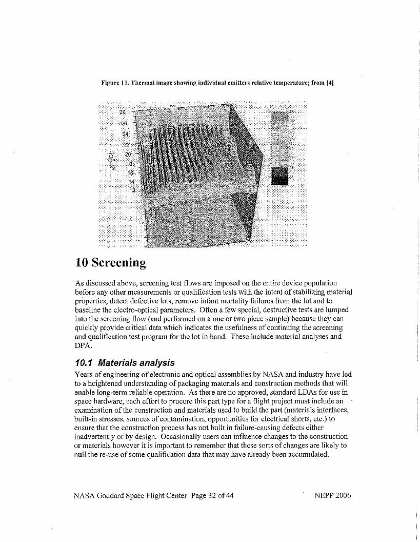
Figure 11. Thermal image showing individual emitters relative temperature; from [4]
10 Screening As discussed above, screening test flows are imposed on the entire device population before any other measurements or qualification tests with the intent of stabilizing material properties, detect defective lots, remove infant mortality failures £rom the lot and to baseline the electro-optical parameters. Often a few special, destructive tests are'lumped into the screening flow (and performed on a one or two piece sample) because they can quickly provide critical data which indicates the usefulness of continuing the screening and qualification test program for the lot in hand. These include material analyses and DPA.
10. I Materials analysis Years of engineering of electronic and optical assemblies by NASA and industry have led to a heightened understanding of packaging materials and construction methods that will enable long-term reliable operation. As there are no approved, standard LDAs for use in space hardware, each effort to procure this part type for a flight project must include an . examination of the construction and materials used to build the part (materials interfaces, built-in stresses, sources of contamination, opportunities for electrical shorts, etc.) to ensure that the construction process has not built in failure-causing defects either inadvertently or by design. Occasionally users can influence changes to the construction or materials however it is important to remember that these sorts of changes are likely to null the re-use of some qualification data that may have already been accumulated.
NASA Goddard Space Flight Center Page 32 of 44 NEPP 2006
The intent of Materials Analysis is to make sure that each material used does not cause contamination to the surrounding hardware in a thermal-vacuum environment, that it is otherwise not disallowed for safety and/or health concerns, that it is not known to react with other nearby materials either within the component itself or within the larger system, and that the dimensions and arrangement of the materials does not lead to short-term fatigue, stress or other type of performance failure. If detailed materials and construction information cannot be obtained from vendor, a DPA can be performed in which all materials and dimensions can be identified as well as their location within the package. Several industry and NASA standards are applicable for discovering suspect materials and configurations during a DPA including EIA-469 and MIL-STD-580. Materials analysis should be the first step performed when checking for potential problems with flying commercial components.
10.2 Vacuum o ufgassing (AS TM 595E) In all cases, where the materials are identified by the vendor or if identified by another method, the non-metallic materials should always be characterized for their outgassing properties in a vacuum environment. Even if hardware and surfaces in the immediate vicinity of the LDA would not be affected by outgassed materials, other systems beyond the immediate vicinity may be affected by the contamination. The information about which systems are susceptible to contamination by outgassed materials is supplied by the lead contamination expert on the project. Laser systems are generally more susceptible than other subsystems.
The ASTM-E595 procedure is considered the NASA standard and provides several data including total mass loss (TML), collected volatile condensable material (CVCM), and water vapor regained (WVR). The test is conducted using pre-bake conditions which are meaningful either for the material (for curing for example) or for the project and then with a 24 hour soak at 125OC at less than Ton. Standard acceptance criteria used NASA-wide are: TML less than 1 .O% and CVCM less than 0.1%. This materials test does not provide definitive information about the composition of the deposited material if an item composed of multiple materials is tested, but as an initial screen it can provide the contamination engineer enough information to assess whether or not to prohibit certain materials, require preprocessing of the materials, or to require additional measures to guard against the potential threat of contamination. Knowing that contamination is such a large failure mode of high power laser systems, this issue is extremely important to space flight laser development engineers.
Material outgassing testing is not always performed on golno go basis. High TML and low CVCM results may be managed using preconditioning (following a re-test to show that the preconditioning treatment is effective). Using preconditioning bakes either prior to LDA installation or afterwards can be logistically difficult because a relatively large chamber may be required and then will need to be decontaminated following the procedure.
NASA Goddard Space Flight Center Page 33 of 44 NEPP 2006

10.3 External Visual inspecfion (M/1,883-2009)
External visual inspection is used to verify that all devices are fiee of defects or damage that can be observed visually with 1.5X to 10X magnification. The test is performed per MIL883-2009.9. As the LDA consists of repeating identical units it is recommendable to establish a nomenclature for addressing the individual units, individual emitters, individual bond wires etc. An overview picture of the complete assembly at low magnification is also recommended for all devices tested. Figure 12 shows an example of an overview picture of SDL G-16 which was being subjected to DPA.141
Figure 12. Example of overview picture for external visual inspection; 6-16 SDL LDA from [4]
10.4 Burn-in (MIL 883- I 0 15.9) As mentioned above the purpose of burn-in is to eliminate devices from the lot that would otherwise fail due to infant mortality. This is usually done by increasing operating temperature, current andlor power of the devices enough to accelerate the initial usage exposure and detect devices with abnormal changes in threshold current or other characteristics during the burn-in. 96 hours at 70°C or the specified highest safe operating temperature at fixed maximum output power has been used in the past based on - . The passlfail criterion is based on threshold current or drive current; less than 5% increase is the goal. Burn-in is usually done by the LDA vendor and can be a step-
NASA Goddard Space Flight Center Page 34 of 44 NEPP 2006
wise procedure starting with burn-in of the individual bars and then final burn-in of the complete LDA assembly before delivery.
10.5 Temperature cycling (GR468-5.20 and MIL883-1010.8) As thermal cycling is an important stress test of the overall mechanical stability of the LDA, a limited number of thermal cycles can also be used as a screening test. The devices are un-powered and the only monitor during the test is the temperature sensor on the device to ensure the correct profile with ramp rates of minimum 1O0C/minute and dwell times of 10 minutes minimum with the number of cycles between 5 and 10 times.
11 Qualification Testing A qualification investigation is conducted to both verify that the part will withstand the space flight environment and to assess long-term reliability by speeding up potential degradation mechanisms that could cause wear-out failures of the devices. Qualification testing is destructive so careful planning of sample allocation is important to manage cost.
11. I Constant acceleration (NIIL883-2001.2) The purpose of this test is to reveal mechanical and structural weaknesses which may lead to failure during launch. Testing is performed on a spin table or similar equipment capable of the specified test acceleration. With the device properly mounted and any leads or cables appropriately secured a constant acceleration of 30,000g (condition E in MIL883-2001.2) is applied for 1 minute along each of the three major axes in both directions (sequence: Xi,X2,Y1,Y2, Zl and Z2). A failure is constituted by any change or movement of any parts or if any basic parameters are changed.
11.2 Accelerated aging (GR468-5.18, FOTP-I30 and MIL883- 1005.8)
Accelerated aging or life testing is intended to demonstrate a sufficient life expectancy for the device. For CW or directly modulated laser diodes, lifetime is measured in the number of operational hours accumulated. For the high power LDAs running in a QCW mode lifetime is expressed in the number of heating and cooling cycles experienced by the device due to the drive pulses, also called "shots". The target is typically in the billions. Figure 13 from [7] shows an advanced life-test station with room for 12 devices and computer controlled and switched instrumentation enabling time-multiplexed measurements of electrical and optical properties for all 12 devices.
NASA Goddard Space Flight Center Page 35 of 44 NEPP 2006
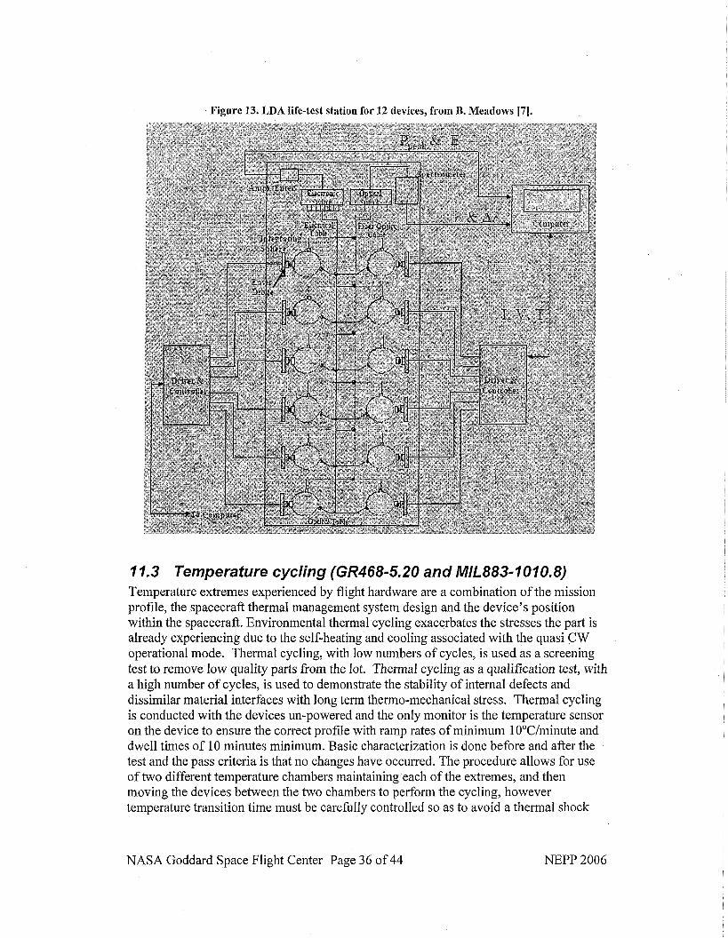
Figure 13. LDA life-test station for 12 devices, from B. Meadows [7].
1 . 3 Temperafure cycling (GR468-5.20 and MIL883-7010.8) Temperature extremes experienced by flight hardware are a combination of the mission profile, the spacecraft thermal management system design and the device's position within the spacecraft. Environmental thermal cycling exacerbates the stresses the part is already experiencing due to the self-heating and cooling associated with the quasi CW operational mode. Thermal cycling, with low numbers of cycles, is used as a screening test to remove low quality parts from the lot. Thermal cycling as a qualification test, with a high number of cycles, is used to demonstrate the stability of internal defects and dissimilar material interfaces with long term thermo-mechanical stress. Thermal cycling is conducted with the devices un-powered and the only monitor is the temperature sensor on the device to ensure the correct profile with ramp rates of minimum 1 O°C/minute and dwell times of 10 minutes minimum. Basic characterization is done before and after the test and the pass criteria is that no changes have occurred. The procedure allows for use of two different temperature chambers maintaining each of the extremes, and then moving the devices between the two chambers to perform the cycling, however temperature transition time must be carefully controlled so as to avoid a thermal shock
NASA Goddard Space Flight Center Page 36 of 44 NEPP 2006
condition. More commonly a single chamber is used with the desired temperature vs. time profile applied to the controller. The temperature extremes used in the test can either be determined as the operational extremes for the complete system or as the default the GR468 values of -4OC to +85C. It is important to understand that this slow but extended range cycling is very much different from the fast and narrow range cycling resulting from the normal QCW operation of the LDA and hence might bring out different failure modes which are packaging related rather than rooted in the semiconductor die.
11.4 Thermal vacuum ~ h e k a l vacuum testing is performed at the instrument and at the spacecraft level. Thermal vacuum testing at the component level is done to reduce cost and schedule impacts associated with component failures late in the mission lifecycle. The profiles shown in the GEVS document can be used as baseline for designing a thermal vacuum test. ,
11.5 Thermal shock (MIL883-1011) Thermal shock testing is a very rigorous test and should only be used when prior evaluations have shown it to be effective for discovering lots with failure modes that could occur during the mission. Where this correlation has not been done the test may be overly extreme and result in irresolvable failures. It requires the device to be submerged in a cold liquid bath (0°C +2"C I-10°C) and then quickly be moved to a hot liquid bath (100°C +lO°C I-2°C).
11.6 Radiafion (MIL883-1019) All types of spacecraft will be exposed to ionizing particle radiation consisting of sub- atomic particles such as protons, heavy ions, alpha particles and electrons. Radiation testing attempts to simulate the effect these different particles, and their different energy levels, have on the device as well as the combined effect caused by all of these particles as energy is continuously deposited into the device over the duration of the mission (total ionizing dose). Qualification tests and application precautions should be based on the specific mission requirements including the thermal environment, the dose rate and the total projected dose.
These mission requirements are generated based on the type of orbit, the mission schedule with respect to the solar seasons, spacecraft shielding and mission duration. Focusing on earth orbiting spacecraft, the LEO (Lower Earth Orbit) missions can see background radiation between 5 to 10 Krads accumulating most of that dose during passes through the SAA (South Atlantic Anomaly). The ME0 (Middle Earth Orbit) path passes through the Van Allen Belts resulting in total dose accumulation between 10 to 100 Krads. The GEO orbit (Geosynchronous Earth Orbit) environment is dominated by dose from cosmic rays to a level of around 50 Krads due to a travel path above the Van Allen Belts. These radiation total dose amounts are based on typical spacecraft shielding and a 7 year mission duration. In cases where the hardware is not shielded by the spacecraft the dose levels can be several orders of magnitude higher, in the Mrads. Table 7. Summary of Missions and Dose Rates summarizes the total dose, mission duration and calculated average dose rate for three recent GSFC missions: GLAS (Geoscience Laser
NASA Goddard Space Flight Center Page 37 of 44 NEPP 2006
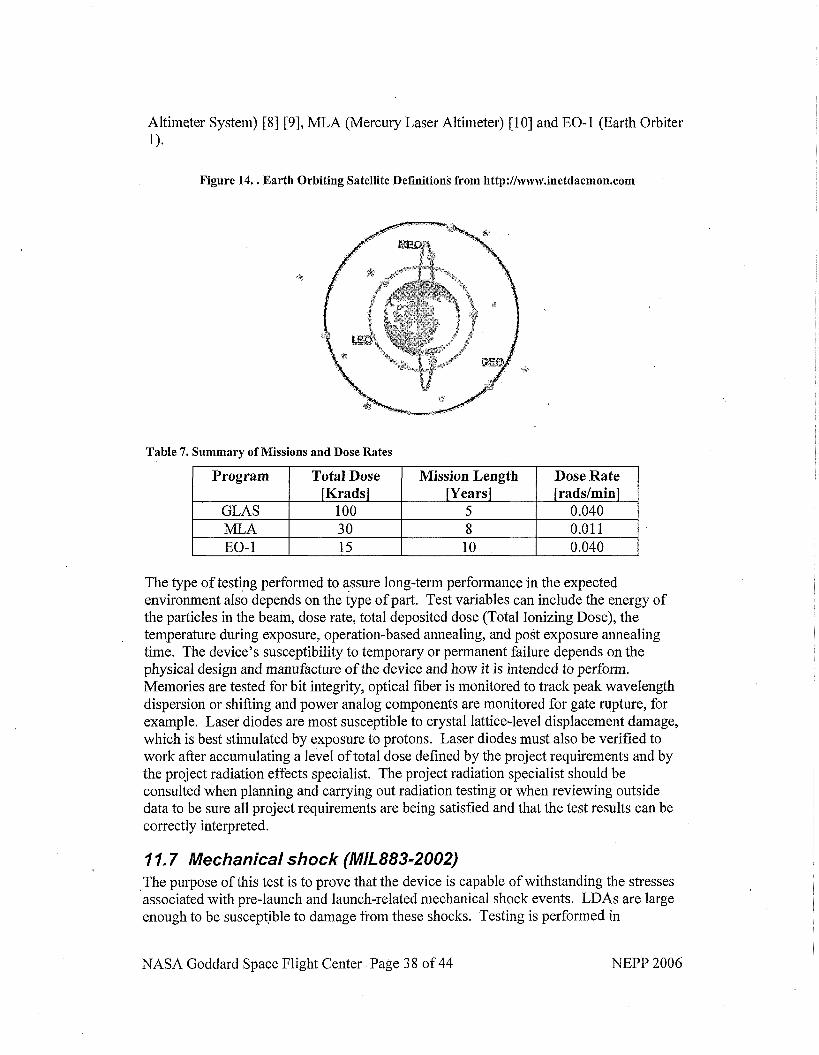
Altimeter System) [8] [9], MLA (Mercury Laser Altimeter) [lo] and EO-1 (Earth Orbiter 1).
Figure 14. . Earth Orbiting Satellite Definitions from http://~~1~)v.inetdaemon.com
Table 7. Summary o f Missions and Dose Rates
The type of testing performed to assure long-term performance in the expected environment also depends on the type of part. Test variables can include the energy of the particles in the beam, dose rate, total deposited dose (Total Ionizing Dose), the temperature during exposure, operation-based annealing, and post exposure annealing time. The device's susceptibility to temporary or permanent failure depends on the physical design and manufacture of the device and how it is intended to perform. Memories are tested for bit integrity, optical fiber is monitored to track peak wavelength dispersion or shifting and power analog components are monitored for gate rupture, for example. Laser diodes are most susceptible to crystal lattice-level displacement damage, which is best stimulated by exposure to protons. Laser diodes must also be verified to work after accumulating a level of total dose defined by the project requirements and by the project radiation effects specialist. The project radiation specialist should be consulted when planning and carrying out radiation testing or when reviewing outside data to be sure all project requirements are being satisfied and that the test results can be correctly interpreted.
Program
GLAS MLA EO- 1
7 1.7 Mechanical shock (MIL883-2002) The purpose of this test is to prove that the device is capable of withstanding the stresses associated with pre-launch and launch-related mechanical shock events. LDAs are large enough to be susceptible to damage from these shocks. Testing is performed in
NASA Goddard Space Flight Center Page 38 of 44 NEPP 2006
Total Dose [Krads]
100 30 15
Mission Length [Years]
5 8 10
Dose Rate [radslmin]
0.040 0.01 1 0.040
accordance with MIL883-2002, Condition B: 5 timeslaxis and direction; sequence: XI, X2, Y1, Y2, Z1 and Z2; 1,50Og, 0.5ms pulse. After the testing, a visual examination is performed with magnification between IOX and 20X to look for resulting damage.
11.8 Random vibration (MIL883-2007) The random vibration test is also performed to show ruggedness in the launch environment. The qualification level should be traceable to the program requirements which are traceable to the launch vehicle. As is the case with all piece-part level testing, the test condition should be more stressful than is used for the instrument or spacecraft qualification. This provides performance margin. The spectral fiequency range for space flight is usually between 20 and 2000 Hz. The random vibration test is typically conducted for 3 minutes for each axis of orientation.
The profile shown in Table 8 is published in the General Environmental Verification Specification for STS and ELV Payloads, Subsystems and Components for payloads of 50 pounds or less [ll]. This is what would be expected at the box or instrument level for protoflight. The term "protoflight" here indicates that qualification of a large amount of test objects to produce real statistical analysis is not possible. The rule of thumb in cases where the "qualification" is on very few samples or engineering models, is to use Profile 1 of Table 8 with the acceleration spectral density levels doubled at the ends of the range. Profile 2 shows the profile that would be used for "protoflight" qualification of a small commercial part or component.
Table 8. GEVS Protoflight Generalized Vibration Levels for Random Vibration Testing.
Functional performance testing to ensure the part still meets the specification given the margin values assigned should be performed after the testing is completed. When possible, in-situ testing is used to detect intermittent electrical connections however sampling rate must be at least twice the vibration frequency. This would be required if the system is expected to be operational during launch or re-entry, such as a system on the shuttle used for health monitoring.
11.9 ESD threshold (GR468-5.22 and FOTP-129) The purpose of this test is to establish the short and long term susceptibility of the LDA to ESD damage using the standard FOTP-129. This method only covers the HBM (Human Body Model) testing approach. Testing is performed from lOOV or lowest known good voltage, up to 15kV. The pulse waveform should have a 10-90% rise time of
Acceleration Spectral Density Levels:
Profile 2 .052 g21Hz
+6 dB1octave .32 g21Hz
-6 dB1octave .052 g21Hz 20.0 grms
Frequency [&I
20 20-50 50-800
800-2000 2000
Overall
NASA Goddard Space Flight Center Page 39 of 44 NEPP 2006
Acceleration Spectral Density Levels:
Profile 1 .026 g21J3z
-t-6 dB/octave .16 g2&k
-6 dB1octave .026 g21Hz 14.1 grms
5-15 ns and a decay time of 130-170 ns. Testing is done in all combinations between any two terminals and with the remaining terminals left unconnected. Before testing the basic DC-characteristics in the form of L-I and V-I curves are measured as a baseline. Pass criterions are typically defined by less than 50% increase in threshold current and less than 100% increase in reverse bias leakage current. Also a significant change in the optical spectrum may constitute a failure.
12 DPA (Destructive Physical Analysis) An important tool for assessing the readiness of an LDA for space use is the DPA (Destructive Physical Analysis) where a small population of devices is taken apart to evaluate the materials and construction and assess potential failure mechanisms arising from incompatible materials, design issues and quality of workmanship. Comparing different DPA specimens also enables an assessment of the homogeneity of the lot and enables the user to identify product changes from prior. builds. Even slight changes in physical/material design can null the usefulness of prior qualification data. Ideally DPA should be done as part of the initial screening to provide an untouched baseline before any other measurements or qualification tests, but typically it is done in parallel or following qualification testing to reduce the cost of the destruct sample lot. DPA methods are also used during failure analysis as an important part of determining the root cause. Failure analysis is enabled by the availability of DPA and external visual inspection data and photographs of "good" parts from the qualification process.
12.1 C-SAM (MIL883-2030) C-SAM (C-mode Scanning Acoustic Microscopy) is a type of ultrasonic measurement where echoes from a specified depth are displayed. The transducer is moved spatially and the reflected signal is displayed as an image of the plane at the focus depth inside an assembly. This test is used to examine the assembly for voids between the die and the heat sink, which can increase assembly thermal impedance and lead to failures. C-SAM requires the parts to be immersed in clean de-ionized water during the test hence a bake- out following the test is required before further testing can be done. CSAM testing and data assessment is highly operator dependant. Test conditions such as the soak time prior to measurements can greatly affect the results, if any of the materials in the design allow the water to diffuse into and fill up the voids making them transparent to the test signal.
12.2 Internal visual inspection (MIL883-201 7) Internal visual inspection within the context of DPA uses the inspection criteria in the test standard but is done during deconstruction of the part rather than prior to lidding and delivery. Internal visual inspection is done at both low magnification (30X-60X) and high magnification (75X-150X) per MIL883-2017. For the microcircuit die, MIL883- 201 3 is referenced within MIL883-20 17. The high magnification portion must include bright field illumination (normal to the viewed surface) in order to discern the types of defects described in the test method. During the low power portion of the inspection, attention is paid to substrate and mounting plate alignment, cracks and damage; die mounting, die location, and die orientation; plating materials; excessive amounts of
NASA Goddard Space Flight Center Page 40 of 44 NEPP 2006
material or contamination with foreign materials or particles. At high magnification (75X-150X) attention is to be paid to die cracks and scribe defects; wire bond integrity and quality.
72.3 Bond strength pull test (MIL883-207 7) The purpose of bond pull testing is to verify sufficient bond strength and to find the occurrences of under-bonded wires, cracked wires, cracked bond pads and contaminated bonds. The test standard defines the acceptlreject criteria based on the wire gauge and bond length.
72.4 Die shear (MIL883-2019) The purpose of this test is to determine the force required to separate the die from the submountheat sink to assess the quality of the materials and procedures used for attaching the die to the submount. A force is applied evenly along one of the short sides of the die (-1-2mm side) while monitoring it visually at a minimum of 1OX magnification. The test standard describes the method for determining a force requirement for the die based on the square area of the attach surface in mm2. Failure depends not only on the value of the shear point but also on the location of the separated material (substrate-to-die attach or die attach-to-die.) Die shear can be performed after the emitter subassemblies are removed £rom the device base plate. The sample size requirement corresponds to the number of die sheared, not the number of full devices tested.
12.5 SEM (MIL883-2018) SEM (Scanning Electron Images) mages are created by scanning a focused electron beam across the surface of the device. The low energy secondary electrons emitted are detected and used to modulate the brightness of a synchronously scanned CRT revealing the surface topography and enabling critical dimension measurements. High energy backscattered electrons can also be separated and used for image formation. Since the backscattering efficiency is a function of atomic weight, this image reveals compositional variations due to average atomic number.
NASA Goddard Space Flight Center Page 41 of 44 NEPP 2006
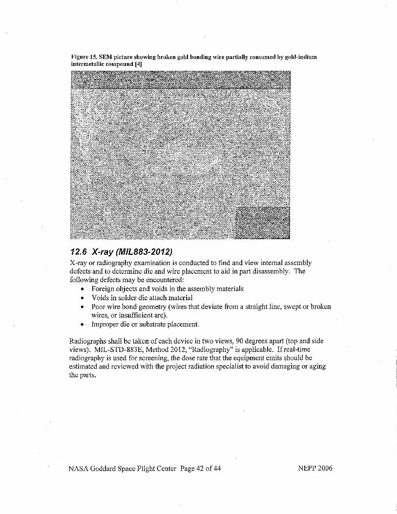
Figure 15. SEM picture showing broken gold bonding wire partially consumed by gold-indium intermetallic compound [4]
12.6 X-ray (MIL883-2012) X-ray or radiography examination is conducted to find and view internal assembly defects and to determine die and wire placement to aid in part disassembly. The following defects may be encountered:
Foreign objects and voids in the assembly materials Voids in solder die attach material Poor wire bond geometry (wires that deviate from a straight line, swept or broken wires, or insufficient arc). Improper die or substrate placement.
Radiographs shall be taken of each device in two views, 90 degrees apart (top and side views). MIL-STD-883E, Method 2012, "Radiography" is applicable. If real-time radiography is used for screening, the dose rate that the equipment emits should be estimated and reviewed with the project radiation specialist to avoid damaging or aging the parts.
NASA Goddard Space Flight Center Page 42 of 44 NEPP 2006
13 References [1 *I Characterization of 808 nm Quasi-constant Wave Laser Diode Arrays, Mark Stephen, Aleksey Vasilyev, 2003 NASA Earth Science Technology Conference for ESTO, NASA GSFC
[l] PEM-NST-001: Instructions for Plastic Encapsulated Microcircuit (PEW Selection, Screening, and Qualzfication, Dr. A. Teverovsky and Dr. K. Sahu, 2003.
[2] High-power 808-nm quasi-CWlaser diode arrays; M. Stephen et. al.; presentation at 4th DAWG meeting in NASA LaRC, 8/16/05.
[3] Optical & Thermal Analysis of High-Power Laser Diode Arrays, A. Vasilyev et. al.; Solid State and Diode Laser Technology Review, Directed Energy Professional Society, Albuquerque, New Mexico, June 2004.
[4] Laser Diode Destructive Physical Analysis Report for CALIPSO, Goddard Space Flight Center Report, Report Number Q30275EV, F. Felt, QSS, September 2003.
[5] Independent GLAS Anomaly Review Board Executive Summary, Internal NASA Goddard Space Flight Center Report November 4,2003. http://icesat.gsfc.nasa.gov/docs/IGARB.pdf or http://misspiggy.gsfc.nasa.gov/tva/meldoc/photonicsdocsAG~report.pdf.
[6] Outgassing Data for Selecting Spacecraft Materials Online, http://outgassing.nasa.gov.
[7] Performance of High Power Arrays Operating in Long Pulse Duration Regime; B. Meadows et. al.; presentation at 4th DAWG meeting in NASA LaRC, 8/16/05.
[8] The Ice, Cloud and Land Elevation Satellite mission: laser radar science for the NASA Earth Observing System, B. E. Schutz et. al., IEEE Geoscience and Remote Sensing Symposium, IGARSS 2000 Proceedings, Vol. 4, July 2000, pp. 1772-1774.
[9] The Geoscience Laser Altimeter System (GLAS) for the ICESat Mission, J. B. Abshire et. a!., Conference on Lasers and Electro-Optics, May 2000, p. 602-603.
[lo] Mercury Laser Altimeter Website, htt~:/fitpwww.gsfc.nasa.go~~/MLA/
[I 11 General Environmental VeriJication SpeciJication (GETS) for STS and ELV Payloads, Subsystems and Components, http://arioch.gsfc.nasa.gov/302/gevs-se/toc.htn1.
[12] Validation of Commercial Fiber Optic Components for Aerospace Environments, International Society for Optical Engineering, M. Ott, SPIE Conference on Smart Structures and Materials, Smart Sensor Technology and Measurement Systems, Vol. 5758, March 2005.
[13] Risk Reduction andAdvancement of High Power Quasi-CW Laser Diode Pump Arrays; F. Amzajerdian et. al.; Solid State and Diode Laser Technology Review, Directed Energy Professional Society, Albuquerque, New Mexico, June 2004.
[14] Improving Reliability of High Power Quasi-CW Laser Diode Arrays Operating in Long Pulse Mode; Farzin Amzajerdian, Byron L. Meadows, Nathaniel R. Baker, Bruce
NASA Goddard Space Flight Center Page 43 of 44 NEPP 2006
W. Barnes, George E. Lockard, Upendra N. Singh, and Michael J. Kavaya; 6th Annual NASA Earth Science Technology Conference, Adelphi, MD, June 26-29,2006.
Acknowledgement Contributors to this document include:
Melanie N. Ott, NASA GSFC Niels Eegholm, ME1
Mark Stephen, NASA GSFC Henning Leidecker, NASA GSFC Jeannette Plante, Dynamic Range Byron Meadows, NASA LaRC
Farzin Amzajerdian, NASA LaRC Tracee Jamison, NASA GSFC
Frank LaRocca, ME1
NASA Goddard Space Flight Center Page 44 of 44 NEPP 2006