Embed Size (px)
Citation preview
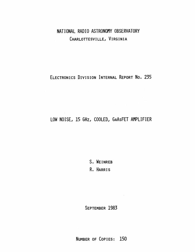
NATIONAL RADIO ASTRONOMY OBSERVATORY
CHARLOTTESVILLEJ VIRGINIA
ELECTRONICS DIVISION INTERNAL REPORT No. 235
LOW NOISE, 15 GHz, COOLED, GAAsFET AMPLIFIER
S. WEINREB
R. HARRIS
SEPTEMBER 1983
NUMBER OF COPIES: 150
LOW NOISE, 15 GHz, COOLED, GaAsFET AMPLIFIER
Table of Contents
I. Introduction • . • • • • • • • • • • • • • • • • • • . . . . 3II. Construction • • • • • • • • • • • • • • • • • • . . 5III. Adjustment and Test . • • • • • • 10
Figures
Figure 1 Amplifier Configuration • . • • . • • • • • . 4Figure 2 Three-Stage Amplifier Without Cover. . • • • 4Figure 3 Schematic of Single Amplifier Stage . • • • • . • • . • 7Figure 4 Amplifier Without Coaxial Components • • • • • • • • . 8Figure 5 Coaxial Components . • . • • • • • • • . 8Figure 6 Middle-Stage View of Amplifier • • • • • . • 9Figure 7 Close-Up View of FET • • • • • . 9Figure 8 Cryogenic Test Configuration • • • • • • . • 11Figure 9 Test Receiver • . • • • • . . • . 11Figure 10 Typical Gain and Noise Temperature . . • . • 12
References • • • • • • • • • • • • 14
Appendices
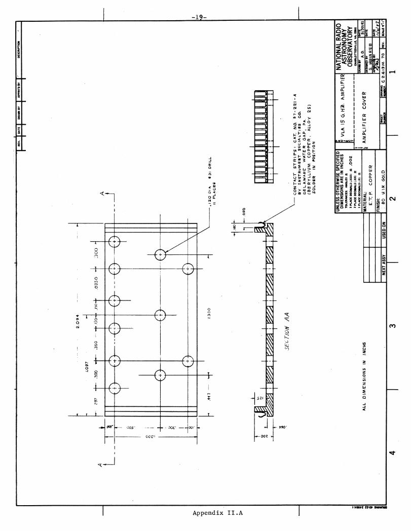
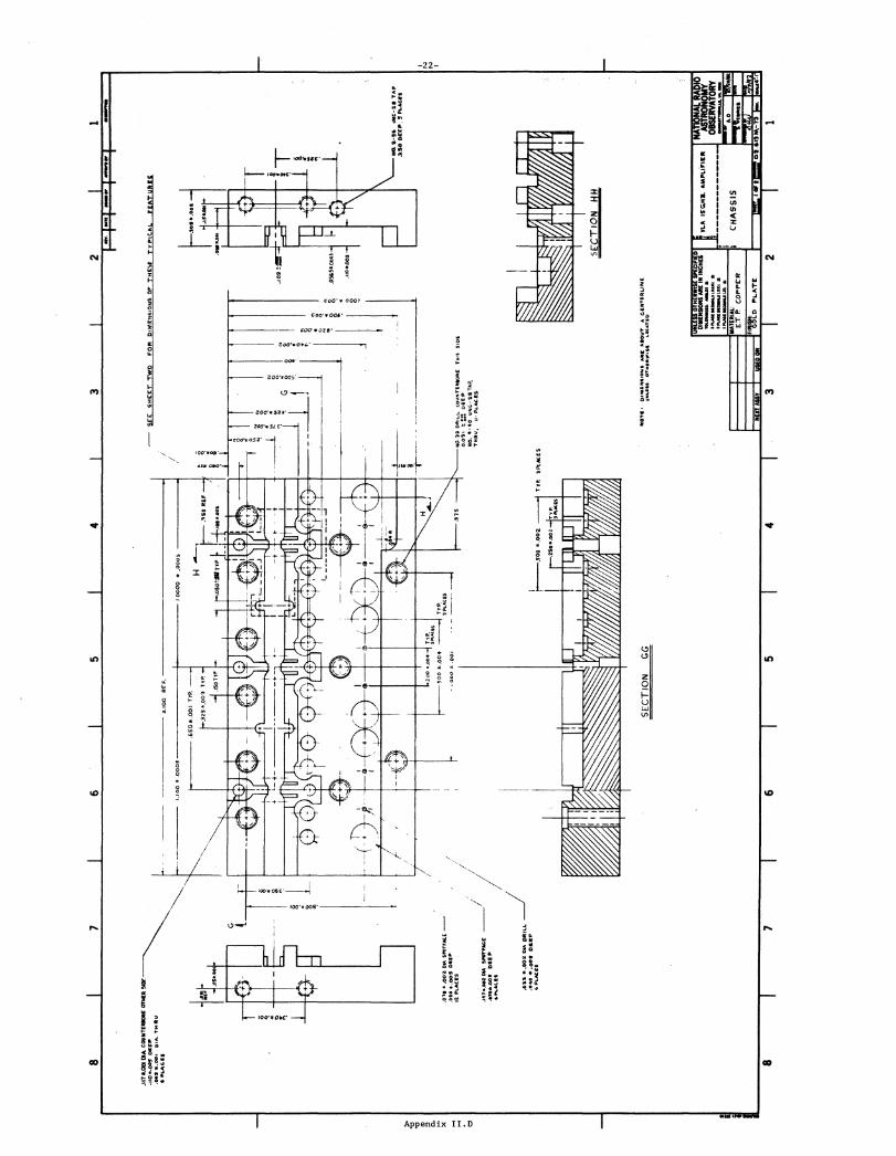
Appendix I Parts List for Ku-Band FET Amp (15.1 GHz) • • • • • • 15Appendix II (Drawings)
. 2.A. Amplifier Cover • • • • • • • ..
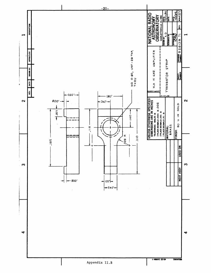
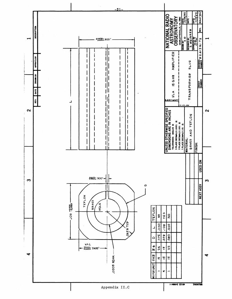
1 09B. Transistor Strap • • • • • . . • .C. Transformer Slug • • • . . 21D. Chassis •• • • • • • • • • • • . . .
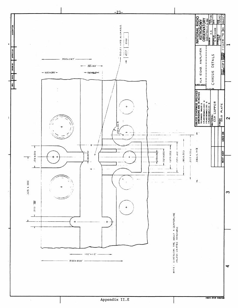
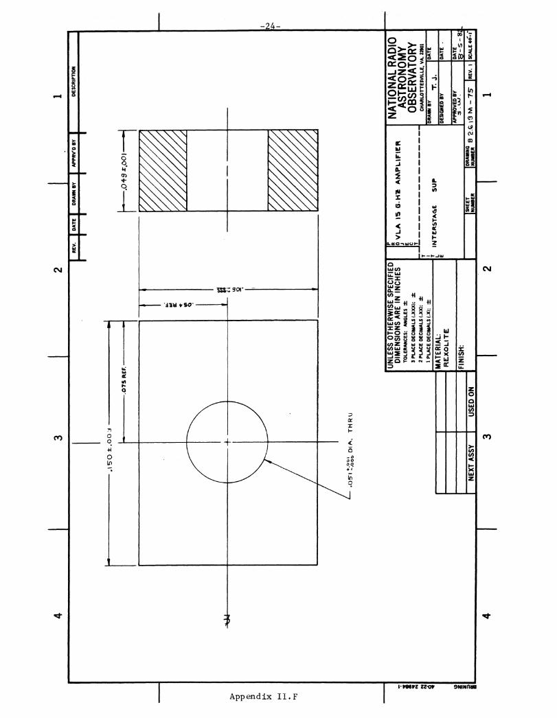
22E. Chassis Details • • • • • • • • • • .F. Interstage Sup. • • • • • • • • • . . 24
• • 2625. . ::
.
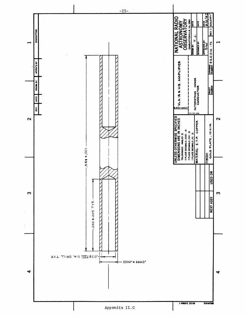
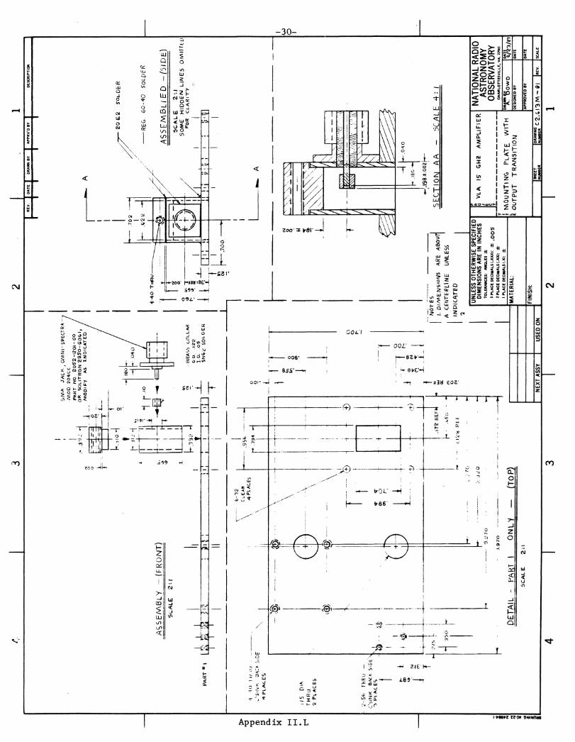
G. Interstage Inner Conductor • • • • • • • • .H. Output Endplate . • . • • • • • • • • • • • .I. Input Endplate • • • • • • • • • • • • • • .J. Input SMA Modification • • • • • • • . . • . . 28K. Output SMA Modification . . . . • • • • • • .L. Mounting Plate with Output Transition • •. . • . 30
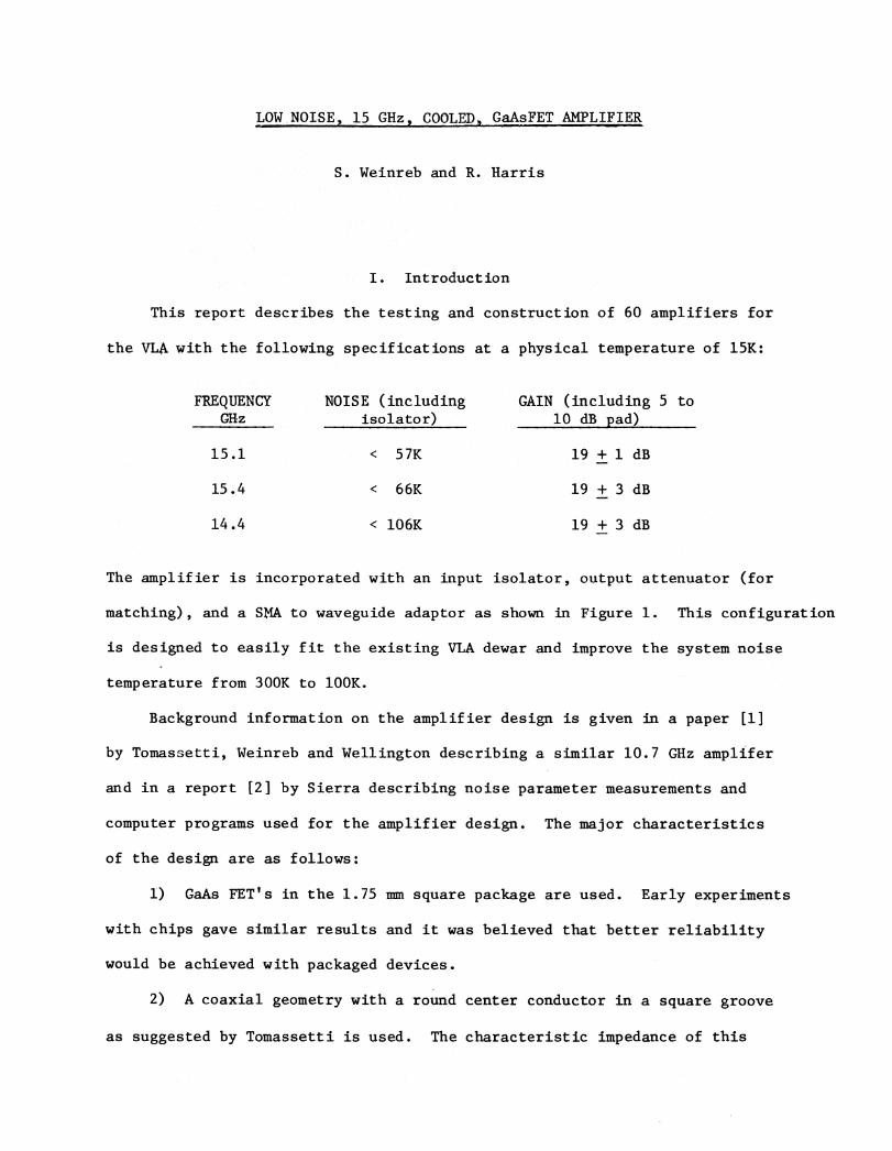
LOW NOISE 15 GHz COOLED GaAsFET AMPLIFIER
S. Weinreb and R. Harris
I. Introduction
This report describes the testing and construction of 60 amplifiers for
the VLA with the following specifications at a physical temperature of 15K:
FREQUENCY NOISE (including GAIN (including 5 toGHz isolator) 10 dB pad)
15.1 < 57K 19 + 1 dB
15.4 < 66K 19 + 3 dB
14.4 < 106K 19 + 3 dB
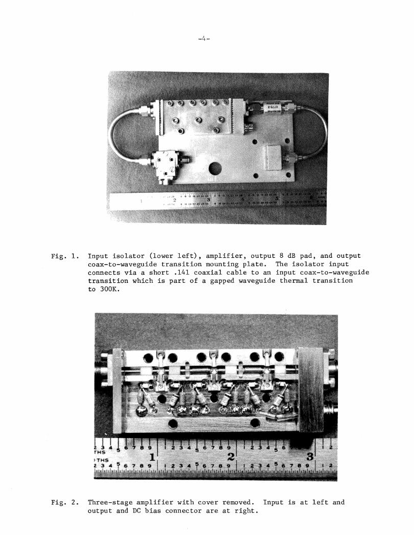
The amplifier is incorporated with an input isolator, output attenuator (for
matching), and a SMA to waveguide adaptor as shown in Figure 1. This configuration
is designed to easily fit the existing VLA dewar and improve the system noise
temperature from 300K to 100K.
Background information on the amplifier design is given in a paper [1]
by Tomassetti, Weinreb and Wellington describing a similar 10.7 GHz amplifer
and in a report [2] by Sierra describing noise parameter measurements and
computer programs used for the amplifier design. The major characteristics
of the design are as follows:
1) GaAs FET's in the 1.75 mm square package are used. Early experiments
with chips gave similar results and it was believed that better reliability
would be achieved with packaged devices.
2) A coaxial geometry with a round center conductor in a square groove
as suggested by Tomassetti is used. The characteristic impedance of this
-4 -
,
4.00ez, tzvl4,4
T H S34
1 1101110111110.100,
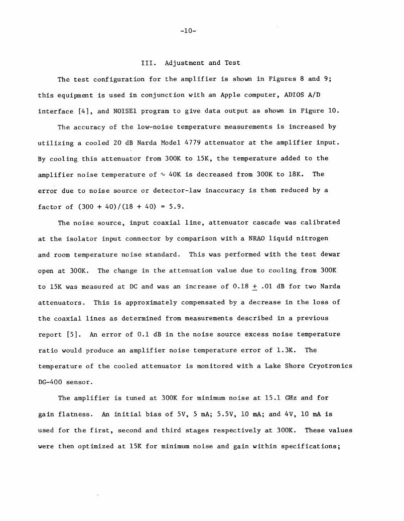
Fig. 1. Input isolator (lower left), amplifier, output 8 dB pad, and outputcoax-to-waveguide transition mounting plate. The isolator inputconnects via a short .141 coaxial cable to an input coax-to-waveguidetransition which is part of a gapped waveguide thermal transitionto 300K.
N
Fig. 2. Three-stage amplifier with cover removed. Input is at left andoutput and DC bias connector are at right.
geometry is given by Wheeler 3]. Tuning is accomplished by moving small X/4
slugs on the center conductor and DC blocks are formed by enclosing the FET
leads, cut to specified length, in Teflon tubing within a hollow center conductor.
DC bias is provided by small wires, X/4 long, soldered directly to the FET
package. This configuration has been found to be reliable, mechanically stable,
repeatable, and amenable to theoretical analysis.
3) The amplifier input and output return loss is reasonable ( 10 dB)
but an input isolator and output attenuator are used to provide > 20 dB return
loss. The FET source lead inductance is kept to a minimum.
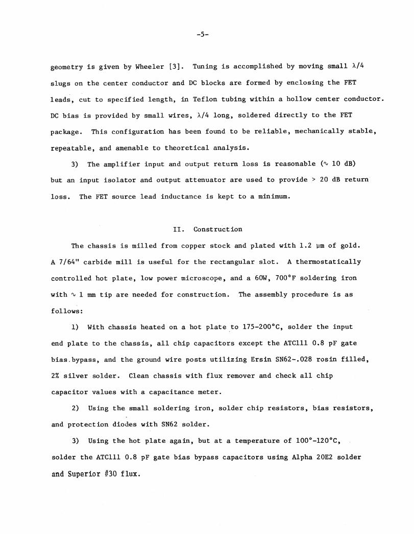
II. Construction
The chassis is milled from copper stock and plated with 1.2 pm of gold.
A 7/64" carbide mill is useful for the rectangular slot. A thermostatically
controlled hot plate, low power microscope, and a 60W, 700°F soldering iron
with q, 1 mm tip are needed for construction. The assembly procedure is as
follows:
1) With chassis heated on a hot plate to 175-200°C, solder the input
end plate to the chassis, all chip capacitors except the ATC111 0.8 pF gate
bias.bypass, and the ground wire posts utilizing Ersin SN62-.028 rosin filled,
2% silver solder. Clean chassis with flux remover and check all chip
capacitor values with a capacitance meter.
2) Using the small soldering iron, solder chip resistors, bias resistors,
and protection diodes with SN62 solder.
3) Using the hot plate again, but at a temperature of 100°-120°C,
solder the ATC111 0.8 pF gate bias bypass capacitors using Alpha 20E2 solder
and Superior #30 flux.
-6-
4) Glue the rexolite support on interstage center conductors as shown
in Figure 5 using Eastman 910 adhesive.
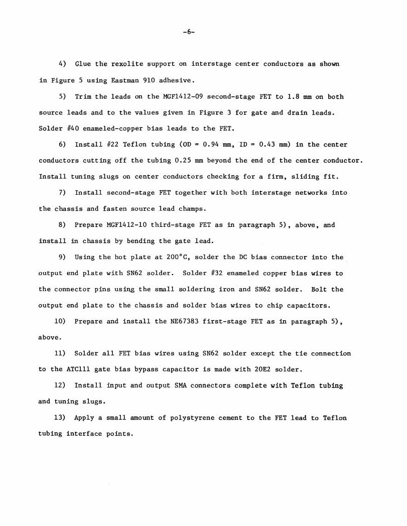
5) Trim the leads on the MGF1412-09 second-stage FET to 1.8 mm on both
source leads and to the values given in Figure 3 for gate and drain leads.
Solder #40 enameled-copper bias leads to the FET.
6) Install #22 Teflon tubing (OD = 0.94 mm, ID = 0.43 mm) in the center
conductors cutting off the tubing 0.25 mm beyond the end of the center conductor.
Install tuning slugs on center conductors checking for a firm, sliding fit.
7) Install second-stage FET together with both interstage networks into
the chassis and fasten source lead champs.
8) Prepare MGF1412-10 third-stage FET as in paragraph 5), above, and
install in chassis by bending the gate lead.
9) Using the hot plate at 200°C, solder the DC bias connector into the
output end plate with SN62 solder. Solder #32 enameled copper bias wires to
the connector pins using the small soldering iron and SN62 solder. Bolt the
output end plate to the chassis and solder bias wires to chip capacitors.
10) Prepare and install the NE67383 first-stage FET as in paragraph 5),
above.
11) Solder all FET bias wires using SN62 solder except the tie connection
to the ATC111 gate bias bypass capacitor is made with 20E2 solder.
12) Install input and output SMA connectors complete with Teflon tubing
and tuning slugs.
13) Apply a small amount of polystyrene cement to the FET lead to Teflon
tubing interface points.
BIAS
GAT
ED
RAIN
6E 13 10
IN82
1"--**
1N
4099
STA
GE L2
L4L5
2.03
2.2
82.
912
2.5
32.5
42.2
83
2.5
32.2
80
STA
GE
Z1LI
L3
I15
1.65
2.5
42
26
1.14
2.0
33
22
1.52
1.78
Fig
. 3
. S
chem
atic
of
sin
gle
am
pli
fier
sta
ge
wit
h u
nit
s of
pF
, o
hm
s, a
nd m
illi
met
ers.
All
tran
smis
sio
n l
ines
are
des
ign
ated
by
th
eir
len
gth
(to
p)
and
char
acte
rist
ic i
mped
ance
;p
rop
agat
ion
vel
oci
ty i
s c
exce
pt
for
.72
c in
39
0 l
ines
. T
he
FE
T's
are
NE
67383 i
nfi
rst
stag
e, M
GF
1412
-09
in s
econ
d st
age,
and
MG
F14
12-1
0 in
thi
rd s
tage
. Len
gths
Li
and
L2
tune
the
am
plif
ier
cent
er f
requ
ency
and
are
cha
nged
by
mov
ing
X/4
tra
nsfo
rmer
slug
s.
-8-
104W, ,V 'A'
,e76,
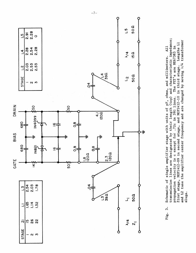
Fig. 4. Amplifier with coaxial components removed.
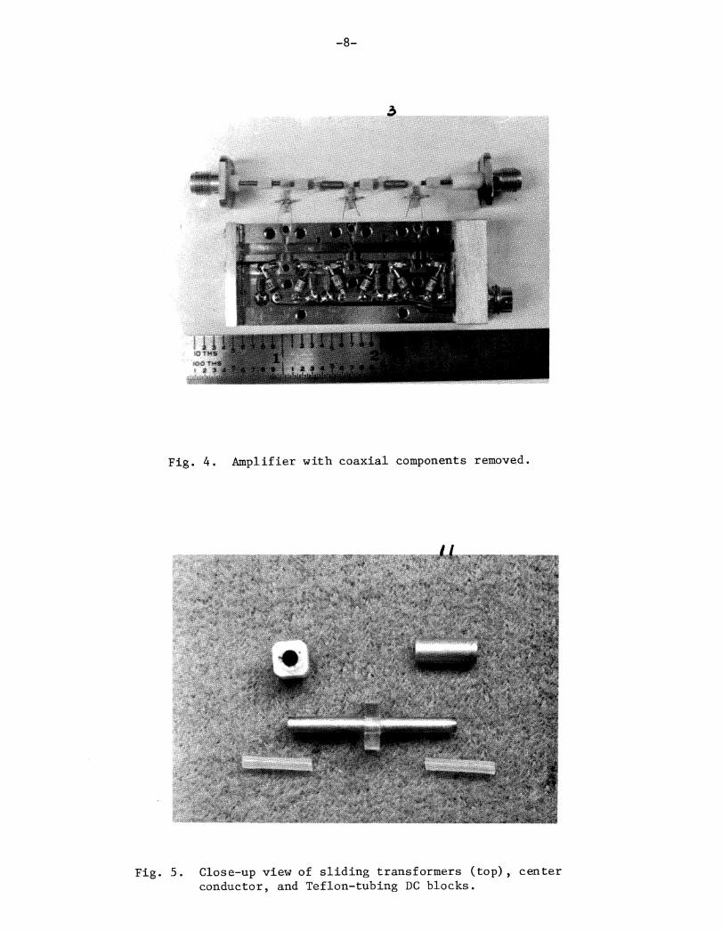
Fig. 5. Close-up view of sliding transformers (top), centerconductor, and Teflon-tubing DC blocks.
-9-
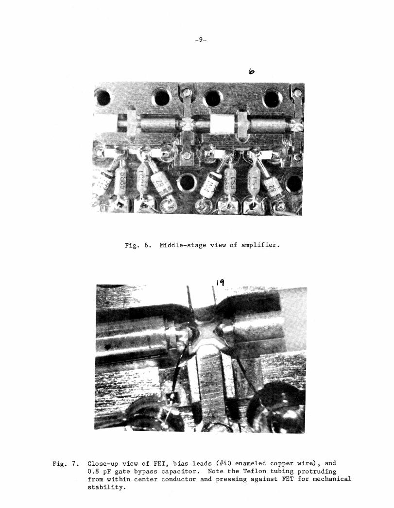
Fig. 6. Middle-stage view of amplifier.
Fig. 7. Close-up view of FET, bias leads (#40 enameled copper wire), and0.8 pF gate bypass capacitor. Note the Teflon tubing protrudingfrom within center conductor and pressing against FET for mechanicalstability.
-10-
III. Adjustment and Test
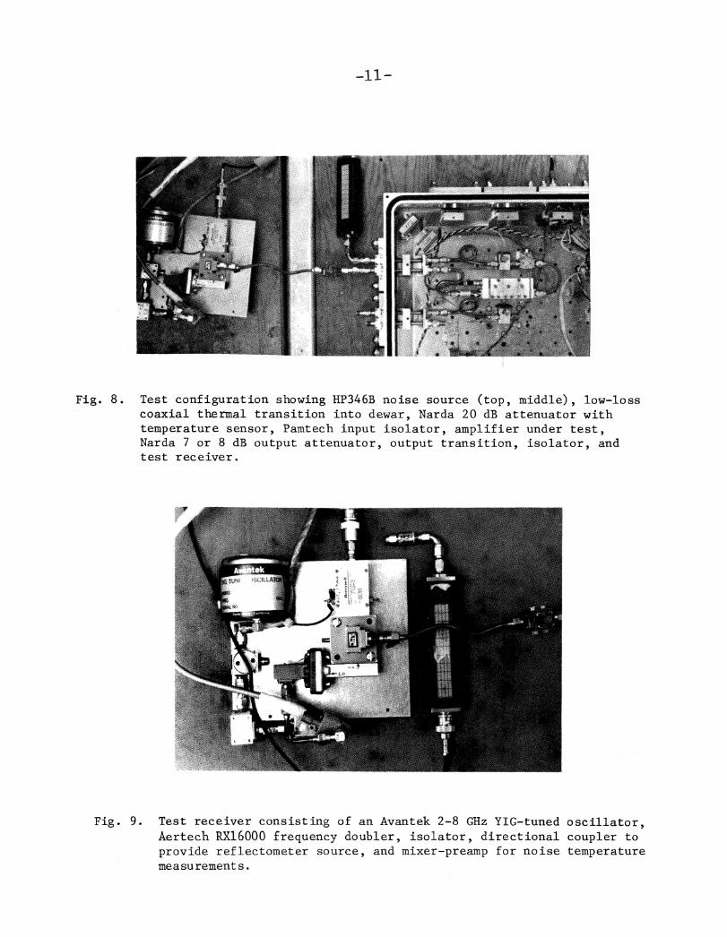
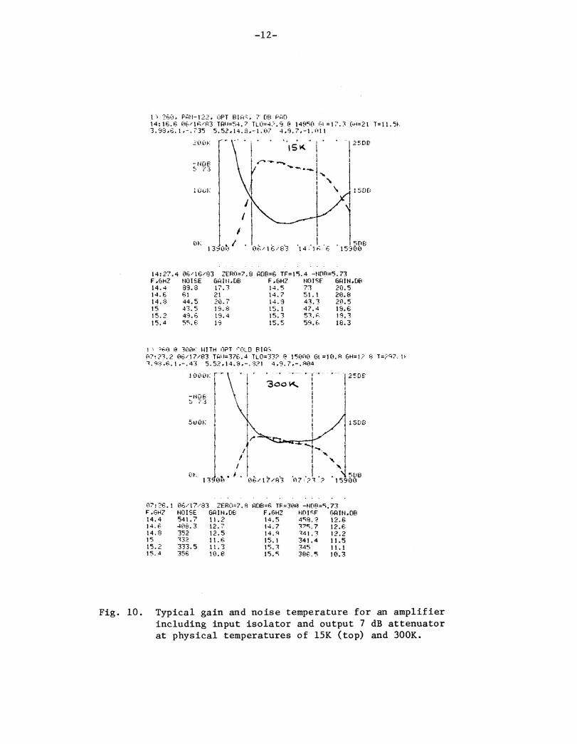
The test configuration for the amplifier is shown in Figures 8 and 9;
this equipment is used in conjunction with an Apple computer, ADIOS A/D
interface [4], and NOISE1 program to give data output as shown in Figure 10.
The accuracy of the low-noise temperature measurements is increased by
utilizing a cooled 20 dB Narda Model 4779 attenuator at the amplifier input.
By cooling this attenuator from 300K to 15K, the temperature added to the
amplifier noise temperature of ix , 40K is decreased from 300K to 18K. The
error due to noise source or detector-law inaccuracy is then reduced by a
factor of (300 + 40)/(18 + 40) = 5.9.
The noise source, input coaxial line, attenuator cascade was calibrated
at the isolator input connector by comparison with a NRAO liquid nitrogen
and room temperature noise standard. This was performed with the test dewar
open at 300K. The change in the attenuation value due to cooling from 300K
to 15K was measured at DC and was an increase of 0.18 + .01 dB for two Narda
attenuators. This is approximately compensated by a decrease in the loss of
the coaxial lines as determined from measurements described in a previous
report [5]. An error of 0.1 dB in the noise source excess noise temperature
ratio would produce an amplifier noise temperature error of 1.3K. The
temperature of the cooled attenuator is monitored with a Lake Shore Cryotronics
DG-400 sensor.
The amplifier is tuned at 300K for minimum noise at 15.1 GHz and for
gain flatness. An initial bias of 5V, 5 mA; 5.5V, 10 mA; and 4V, 10 mA is
used for the first, second and third stages respectively at 300K. These values
were then optimized at 15K for minimum noise and gain within specifications;
Tum ,SCILLA
Fig. 8. Test configuration showing HP346B noise source (top, middle), low-losscoaxial thermal transition into dewar, Narda 20 dB attenuator withtemperature sensor, Pamtech input isolator, amplifier under test,Narda 7 or 8 dB output attenuator, output transition, isolator, andtest receiver.
Fig. 9. Test receiver consisting of an Avantek 2-8 GHz YIG-tuned oscillator,Aertech RX16000 frequency doubler, isolator, directional coupler toprovide reflectometer source, and mixer-preamp for noise temperaturemeasurements.
12502
5DO
° K „ / .00 / 1 '6/8 '7 l4• 1 F. t 15900
- • v20 0 Y. r" . . • I .
ISK
Sireft.-NOB'3 73
I 0 c.;1.;
1) 260, PH-t22, OPT 8IW, 7 OB PAD14:16.6 06/16/63 TA I )=54.7 TL0=4?.9 1490 1,1=17.3 604=21 T=11.51,3.93,6.1,-.735 5.52,14.8,-1.07 4,9.7,-1.'111
14:27.4 06/16/83 ZERn=7.8F.GH2 NOISE GAIN,DB
DB=6 TF=15.4 -1OR=5.73F,GH2 NOISE' GAIN,08
14.4 89.3 17.7 14.5 71 20.514.6 61 21 14.7 51.1 20.814.8 44.5 20.7 14.9 43.7 20.515 47.5 19.8 15.1 47.4 15.615.2 49.6 19.4 15.3 57.1; 19.715.4 55.6 19 15.5 59.6 18.3
1 0 3001, NITH OPT ''OLD BIAS07127.2 06/17/83 TA0=376.4 TL0=33?I 15000 61=10.R GH=1? T=?q7.11
. 5.52,14.8,-.3?1
07:26.1 06/17/83 ZER0=7.8F.13H7 NOISE 6AIN,D6
DB=6 TF=300 -1OP=9.73F,61-1.7 NOIc.F GAIN,08
14.4 541.7 11.2 14.5 4c9.'› 12.614.6 408.3 12.7 14.7 37.;•7 12.614.8 352 12.5 14.q ' 411.1 12.215 732 11.6 15.1 341.4 11.515.2 333.5 11.3 15.7 349 11.115, 4 356 10.8 15. 386.5 10.3
Fig. 10. Typical gain and noise temperature for an amplifierincluding input isolator and output 7 dB attenuatorat physical temperatures of 15K (top) and 300K.
-13-
typical final values were 4V, 5 mA; 5.5V, 15 mA; and 4V, 8 mA. The amplifier
gain including a 7 dB pad is typically 12 dB at 300K and 19 dB at 15K as
shown in Figure 10. The typical improvement in noise temperature is a factor
of A, 8.
A large variation of cold noise temperature with the NE67383 transistor
batch was observed. An initial batch of 20 averaged 35K at optimum frequency;
a second batch 40K; and the third batch 47K. The lowest noise temperature
was 31K and A, 15% of the transistors gave noise temperatures > 50K and were
rejected. Early tests with the NE13783 produced noise temperatures above 60K.
-14-
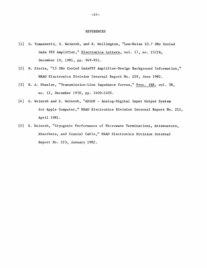
REFERENCES
[1] G. Tomassetti, S. Weinreb, and K. Wellington, "Low-Noise 10.7 GHz Cooled
GaAs FET Amplifier," Electronics Letters, vol. 17, no. 25/26,
December 10, 1981, pp. 949-951.
[2] M. Sierra, "15 GHz Cooled GaAsFET Amplifier-Design Background Information,"
NRAO Electronics Division Internal Report No. 229, June 1982.
[3] H. A. Wheeler, "Transmission-Line Impedance Curves," Proc. IRE, vol. 38,
no. 12, December 1950, pp. 1400-1403.
[4] G. Weinreb and S. Weinreb, "ADIOS - Analog-Digital Input Output System
for Apple Computer," NRAO Electronics Division Internal Report No. 212,
April 1981.
[5] S. Weinreb, "Cryogenic Performance of Microwave Terminations, Attenuators,
Absorbers, and Coaxial Cable," NRAO Electronics Division Internal
Report No. 223, January 1982.
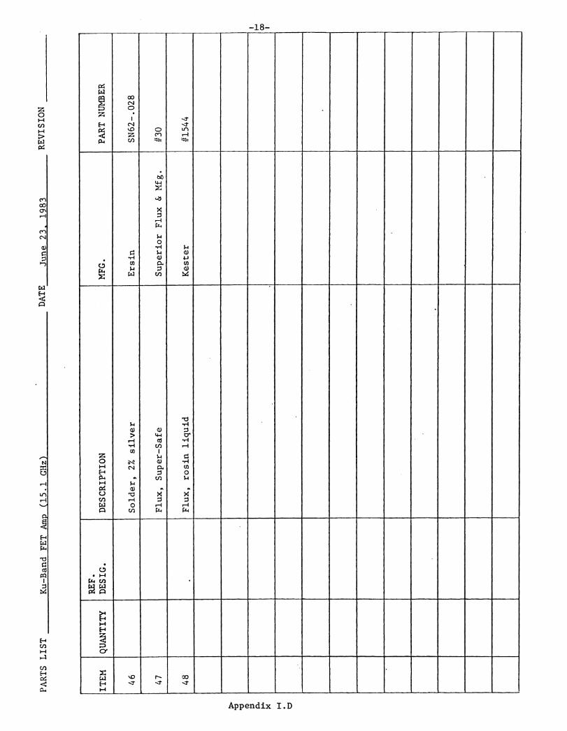
PARTS LIST
Ku-Band FET Amp (15.1 GHz)
DATE
June 23, 1983
REVISION
ITEM
QUANTITY
REF.
DESIG.
DESCRIPTION
MFG.
PART NUMBER
11
15 GHz FET amplifier schematic
NRAO
A2.613S-01
21
Chassis
NRAO
D2.613M-73,
sht.
1,
Chassis details
NRAO
C2.613M-73,
sht.
2
41 6
_Amplifier cover
Transistor strap
NRAO
NRAO
C2.613M-70
B2.613M-71
5
1Output end plate
.NRAO
B2.613M-77
_
.1
Input end plate
NRAO
B2.613M-78
,
4Transformer slug (15 ohm)
,
NRAO
B2.613,M-72
1Transformer slug (26 ohm)
NRAO
B2.613M-72
101
Transformer slug (22 ohm)
NRAO
B2.613M-72
112
Interstage support
NRAO
B2.613M-75
,
122
.Interstage inner conductor
.NRAO
B2.613M-76
131
Mounting plate with output transition
NRAO
.
C2.613M-81
,
141
Input SMA modification
Omni-Spectra (modified)
204CC/NRAO B2.613M79
151
..._
Output SMA modification
Omni-Spectra (modified)
_
204CC/NRAO B2.613M80
PARTS LIST
Ku-Band FET Amp (15.1 GHz)
June 23, 1983
REVISION
DATE
ITEM
QUANTITY
REF.
DESIG.
DESCRIPTION
MFG.
PART NUMBER
164
SMA connector
Omni-Spectra
201-1A
171
Power connector
Micro-Tech
ER-7S-6
186
X/4 transformer dielectric, Teflon
Alpha
AWG-24-LW
191
FET
first stage
NEC
NE67383
201
FET, second stage
Mitsubishi
MGF-1412-09
IFET bias leads, 40 AWG T2 Beldure
;-e-
8046
242
Finger stock
Instrument Specialties
256
0-80 x 3/16 Filister HD screws (goldplated
26
84-40 x 3/16 socket HD SS screws
All-Metal
273
4-4
0 x
5/1
6 socket HD SS screws
All-Metal
282
2-5
6 x
1/2
socket HD SS screws
All-Metal
29
42-5
6 x
1/4
so
cket
HD SS screws
All-Metal
302
2-5
6 x
3/1
6 socket HD SS screws
All-Metal
PAR
TS
LIS
TK
u-B
aad
FF
T A
mp
(1
5.1
(1
14
z)
June
23,
1983
REV
ISIO
ND
ATE
ITEM
QU
AN
TITY
REF
.D
ESI
G.
DES
CR
IPTI
ON
MFG
.PA
RT N
UM
BER
31,-
3.8
pf
ch
ip c
ap
acit
or
ATC
111T
BA
OR
8B10
0AP
326
.8 p
f ch
ip c
ap
acit
or
ATC
100A
0R8C
P50
336
16
pf
ch
ip c
ap
acit
or
ATC
100A
160C
P50
346
680 p
f chip
capacit
or
ATC
100B
681K
P5O
X
356
50 o
hm
chip
resi
stor
Min
i-S
yst
ems,
Inc.
WA
13PG
-500
J-S
363
49
.9 o
hm
1/8
W m
etal
fil
m r
esis
tor
Cor
ning
RL
RO
5C-4
9R9-
FR
373
1000 o
hm
1/8
W m
etal
fil
m r
esis
tor
i1i,
iR
O5C
-100
1-FR
38•
3D
iod
e ze
ner
Mot
orol
a1N
4099
393
Dio
de
zen
erM
otor
ola
1N82
1
401
7 d
B a
tten
uat
or
DC
-18 G
Hz
Nar
da47
79-7
411
Co
ole
d i
sola
tor
Pam
Tec
hPT
C-2
021M
42.
.141 s
emi-
rigi
d co
ax,
50 o
hm
.U
nifo
rm T
ubes
UT
-141
A
43P
oly
sty
ren
e Q
-do
pe
GC
Ele
ctro
nic
s#3
7-2
44910
adhes
ive
Per
mab
ond I
nte
rnat
ional
910
45S
old
er B
20
E2
,.0
32 d
ia.
Alp
ha
Met
als
B20
E2-
.032
PAR
TS
LIS
TK
u-B
and
FE
T A
mp
(15.
1 G
Hz)
Jun
e 23,
1983
REV
ISIO
ND
ATE
ITEM
QU
AN
TITY
REF
.D
ESI
G.
DES
CR
IPTI
ON
MFG
.PA
RT N
UM
BER
,,
46S
old
er,
2%
sil
ver
,E
rsin
SN
62-.
028
,,
47F
lux,
Super
-Saf
eS
up
erio
r F
lux
& M
fg.
#30
48.
Flu
x, ro
sin l
iquid
Kes
ter
#154
4
,
.,
,
..
,
VLA
15 G
. H
E. AM
PLI
FIER
UN
LE
SS O
TH
ER
WIS
E S
PEC
IFIE
DD
IME
NSI
ON
S A
RE
IN
IN
CH
ES
TO
LERAN
CES:
AN
GLE
S *
3 PL
ACE
DEC
IMALS
(.X
XX1:
. 002
2 P
LACE D
ECIM
ALS
I.X
/0:
*
I PLA
CE D
ECIM
ALS
00:
*
REV
.D
ATE
DRAW
N B
YAPP
IWO
BY
DES
CRIP
TIO
N
2.0
94
1.097
.3so
.iso-
. 0350
"300 J -
297
.300
0 0
01
rt:1 CD P.,
4
.41
7 -
-to
rel
1.300
>4
.120 D
I A
31 D
RIL
LIL P
LA
CE
S
L.
-#.111
111 .1
1111
1r../
.111
1"%
1111
111
11M
1111
1/>
,
SE
LT
/ON
AA
CO
NT
AC
T S
TR
IPS
: C
AT
. N
O. 97-2
2I-
AB
y I
NS
TR
vAA
BR
IT S
Ec.
/A L
l-i E
S C
O.
DE
LA
WA
RE
WA
TE
R G
AP
, P
A.
(BE
RYLLIVAA C
OP
PE
R , A
LL
OY
25)
SO
LD
ER
1W
PO
SiT
iON
MA
TER
IAL:
AM
PLIF
IER C
OVER
Ur
P. C
OP
PE
R
FIN
ISH
:. 8
0 I
A I
N. G
OL
D
NATI
ON
AL
RAD
IOASTRO
NO
MY
OBSERVATO
RY
CH
ARLO
TTES
VILL
E. V
A. n
un
DRAM
MY
DATE
A.D
.9/
30/1
2DE
saric
o BY
DATE
S. E
INR
EB
V B
YD
ATE
/I7
REV
. SCALE
AL
L D
IME
NS
ION
S I
N I
NC
HS
NEX
T AS
SYU
SED
ON
SH
EET
HU
MM
ERD
RAW
ING
Num
BER.
C 2
.61
3M
70
43
21
FINI
SH:
BO
U I
N. G
OLD
NEX
T AS
SYU
SED
ON
DA
TED
RAW
N BY
APP
RV
'D B
YD
ESCR
IPTI
ON
.18
5
.118
UN
LESS
OTH
ERW
ISE
SPEC
IFIE
DD
IMEN
SIO
NS
ARE
IN I
NCH
EST
OL
ER
AN
CE
S: A
NG
LE
S *
3 PL
AC
E D
ECIM
ALS
(.X
XX
):. 0
02
PLA
CE
DEC
IMA
LS (.
XX
):1
PLA
CE
DE
CIM
AL
S (.X
): *
ORPV
LA
15
G.H
. AM
PLI
FIER
NAT
ION
AL R
ADIO
AST
RO
NO
MY
OBS
ERVATO
RY
/MAT
ERIA
L:B
RA
SS
-T L
CH
AR
LOTT
ESV
ILLE
, VA
. 229
01D
RAW
N BY
TR
AN
SIS
TO
RS
TR
AP
A. D
.tO
1/
82,
DA
TE
.D
ESIG
NED
8
AP
P74
OA
T ,
.3(g
2-M
EE
T! N
UM
BER
!DRA
WIN
G!N
UM
BE
R B
2.6
1 3
M 7
tIR
EV.
SCA
LE 2
0'..1
'
.02
5
II
II
I
r41
,_
NO
. 0-
60, U
NF
28 T
AP,
THRU
FV"-
0
v).
.06
0
-
4I
32
1
4I
31
DESC
RIPT
ION
. NaP
ERU
N1T
GH
EE
4D
L, T
EF
LO
N
I15
26
.075
.2.0
0NO
415
15.
.079
.198
YE
S,
152.
2
, .080
.200
NO
,, ,
MA
TER
IAL:
BRAS
S A
ND
TEFLO
N
UN
LE
SS O
TH
ER
WIS
E S
PEC
IFIE
DD
IME
NSI
ON
S A
RE
IN
IN
CH
ES
TOLE
RAN
CES:
AN
GLE
S *
3 PL
ACE
DEC
IMAL
S (.
XXX)
: *
2 PL
ACE
DEC
IMAL
S (.
XX):
*1
PLAC
E DE
CIM
ALS
(.X):
lP
R 0 J E V
L A
c I. .11
•111
, IM
MO
ON
O M
INN
ID II
IIIN
D S
EIM
TRAN
SFO
RM
ER
SL
UG
15 G
.HE
'I MO
MIN
I =
NM
NU
M M
UM
ON
O 11
111111
P
DRAW
N BY A
. 0DE
SIGN
ED B
YS
. WE1N
REB
CHAR
LOTT
ESVI
LLE,
VA.
229
01D
ATg
/0/0
6/82
DAT
E .
APP
R,V
4347
FIN
ISH
:SC
ALE
30:
e
DAT SI3
Z.
USE
D O
NN
EXT
ASS
Y
f,............................•,,,,....,....,..........,*,...
...,....
.......
.:,.....,
,
3
1D
RAW
N B
YAP
PRV'
D B
Y
NAT
ION
AL R
ADIO
AST
RO
NO
MY
OBS
ERVATO
RY
'DRA
WIN
G,
,,,,
'NU
MBE
R °
nn ,
I SHE
ET/N
UMBE
RRE
V.
REV.
DATE
AM
PL
IFIE
R
.050
5 R
EA
M
32
1
.117
*.00
1EO
UN
TEREO
RE
WEE
R S
W•1
10 2
.005
DEE
P.*
*3*.0
0•
otA
. TN
RV
Pi..
AG
EE2.1
00 R
EF.
1.1
00 .
0005
10000 *
.0005
315$
.00I
NO
. E-S
i O
NC-2
11 T
AP
.1E0 D
EEP,
5 PL
ACES
2 o
0 .
004
500 I
- .004
- 000 .
001
Igik
s
NO
32 D
R.,
covN
TEARO
RE T
A,S
StD
E4
.3
1 t 'l
lt D
EEP
NO
. 4
-40
UN
C-2
0 T
AP
,TsR
u,
PL A
C E
S.I
474.
002
DIA
SPO
T,AC
E.0
7••
•00,
DEEP
• ..
.ALE
S
.011 2
.002 D
IA D
RIL
L.•
•• .
.00s
PG
PL
AC
ES
.500
2.0
02
TYlt 3
PLAEES
1111
1111
1111
1111
;mom
VS
At
ASECTIO
N H
H
SECTIO
N G
G
NO
TE
ME
NS
tON
II A
A.
AEO
UT. A
CE
NT
ER
LIN
EV
NL
EE
S 0
,461
1V/t
Et
...A
TO
M
UNLE
SS O
THER
WIS
E SP
ECIF
IED
DIM
ENSI
ONS
ARE
IN IN
CHES
TO
LEAN
CE* A
NIN
111 *
*AIX
ALP
IIALS
(M
UM
*KAU
I.XXI:
*1
PUCE
OCC
INAL
S
YL
A 1
5%/4
111
AM
PLIP
ItIt
MATERIA
L:
ET
P C
OP
PE
RC
HA
SS
IS
NEXT A
SSY
A. D
.D
itTh7/8
2
RAW
INR
C 2
.6i3
M -
73 R
EV.
REV
.D
ATE
DRAW
N B
YAPP
RV
. 0 B
Y
.32
5' t
.003
-1.04
0 REF
.1-.--
4-f
O't 0
H.■
2 5:1
7,0
022
-
.1
80±
.00
3
NO- T
E. •
DIM
EN
SIO
NS A
RE A
BO
UT A
CEN
TERLI
NE
UN
LESS L
ocATEC O
TH
LBIN
F.if
UN
LE
SS O
TH
ER
WIS
E S
PEC
IFIE
DD
IME
NSI
ON
S A
RE
IN
IN
CH
ES
TO
LERAN
CES:
AN
GLE
S ±
3 PL
ACE
DEC
IMALS
(.X
XX):
2 PL
ACE
DEC
IMALS
(XX):
1 PL
ACE
DEC
IMALS
(.3
0:
MA
TER
IAL:
E:T
.P C
OP
PE
R
0VLA I
SG
HZ.
AM
PLIF
IER
CH
ASSIS
DETAIL
S
NA
TIO
NA
L R
AD
IOA
ST
RO
NO
MY
OB
SE
RV
AT
OR
YCH
ARLO
TTES
VIL
LE,
VA.
2290
1
DES
IGN
ED B
YS.
WEIN
R E
B
DRAM
BY
DATE
FIN
1$H
:G
OLD
PL
AT
E
APPR
IEag
i°,
1$/r
7SCALE
15't
1'SH
EET EN
2 F
2N
EX
T A
SSY
USE
D O
N
44' 0 co
DES
CRIP
TIO
N
OR I
//
002
RID
uEti +
002
Au o
vvABLE
4-
1.05
1t.0
01 R
.109
±.0
02
C
21
DATE
DRAW
N BY
APPR
V*13
BY
DESC
RIPT
ION
I
REV.
N.)
.051
TH
R U
UN
LESS
OTH
ERW
ISE
SPEC
IFIE
DD
IMEN
SIO
NS
ARE
IN I
NCH
ESTO
LERAN
CES:
AN
GLE
S ±
3 PL
ACE
DECI
MAL
S (.
XXX)
:2
PLAC
E D
EC
IMA
LS
(.x
x):
1 PL
ACE
DECI
MAL
S (.X
): :.
+:
IR 0 v
LA
15
G.H
Z A
MP
LIF
IER
IE ICJT
NAT
ION
AL R
ADIO
AST
RO
NO
MY
OBS
ERVATO
RY
CHAR
LOTT
ESVI
LLE.
VA .
229
01D
RAM
BY
DATE
MAT
ERIA
L:R
EX
OL
1TE
INTERSTAG
E SU
PDE
SIGN
ED B
YD
ATE
.
NEX
T AS
SYFI
NIS
H:
USE
D O
N
APPR
OVE
D B
Y5 •
LA
./ .
'SH
EE
T'D
RA
WIN
G'N
UM
BE
R'N
UM
BE
R2.
6 iS
M—
75
IREv
. 1
DATE
Z3 SCAL
E 40; r
31
21
41
.150 t.001
h
- .0
+91
. .001
-el
. 075 R
EF.
43
21
P.t
SHEE
TDR
AWIN
GNU
MBE
RN
UM
BE
R
2•G
13
M -
76
REV.
I
43
1RE
V.DA
TEDR
AWN
BYAP
PRIP
D B
YDE
SCRI
PTIO
N
6 4
4 *
,00
t
.200*.0
05 T
YP.
111■1
1011■
11■110
110111
■11■ W
ILM
IZIM
MIN
I■11
1011
k WW
1111
6110
11:11
1011
1211
0101
1011
0110
1111
0111
■111
■111
~116
.1
Iihal
lINI M
Mb.11
16111■
711■11
111011
■111■1
11■11
~111■
111011
1:1111
M.
II KIII
MM
ICIL
NIM
MIM
IIMM
ILN1
11■1
116.1
1101
16.11
1101
1■11
■
4
NEXT A
SSY 3
USE
D O
N
UN
LESS
OTH
ERW
ISE
SPEC
IFIE
DD
IMEN
SIO
NS
ARE
IN I
NCH
ESTO
LERAN
CES:
AN
GLE
S ±
3 PL
ACE
DECI
MAL
S (.
XXX)
:2
PLAC
E DE
CIM
ALS
(.XX)
:1 P
LACE
DEC
IMAL
S (.X
):
MATE
RIA
L: E
.T.P
. C
OP
PE
R
FINI
SH:
GO
LD
PL
AT
E ,
10 L
IAM
.
lPR 0
NIL
/1/4
IS 6
.1-M
. AM
PLI
FIE
RJ E C T
INT
ER
ST
AG
E. I
NN
ER
EC
ON
DU
CT
OR
NAT
ION
AL R
ADIO
AST
RO
NO
MY
OBS
ERVATO
RY
CHAR
LOTT
ESVI
LLE,
VA.
229
01D
ATE
DESI
GNED
BY
APPR
OVE
D B
YCr‘i 1
DRAW
N BY
T.
J.
DAT
E .
DATE
SCAL
E Z
IA
.0 9
5 .
0 01
DIA
. D
RIL
L ,
THR
U
. 50
0 *
.00
I D
IA. B
OR
E9*.0
01 D
EEP
UN
LESS
OTH
ERW
ISE
SPEC
IFIE
DD
IMEN
SIO
NS
ARE
IN I
NCH
ESTO
LER
AN
CES
: AN
GLE
S
3 PL
AC
E D
ECIM
ALS
(.X
XX
):2
PLA
CE
DEC
IMA
LS (.
XX
):1
PLA
CE
DEC
IMA
LS (.
)0:
DR
AWN
BY
T. .
J.D
ATE
DA
TE
DA
TEe .
5 V
.Z..
SCA
LE
MA
TE
RIA
L:
E.T
. P
. C
OP
PE
RD
ESIG
NED
BY
APP
RO
VED
BY
t.s.1
REV.
IF
INIS
H:
80 V
AN
. G
OL
DU
SED
ON
!SH
EET
I DRA
VA N
GN
UM
BER
INu,
mE
R
8 2
.6 4
3 M
-
1
REV
.D
ATE
DRA
WN
BY
APP
I1V
ID B
YD
ESC
RIP
TIO
N
NO
. 2-S
11 L
ING
- 2
E1
TA
P, T
HR
Ua-
RE
AM
..1
615
D1A.
THRU
.525 .
002
.312 H
OL
E T
HR
Utis
.340*.0
01
.32
5±
.001
.170
REF
.
44
so.
•94
11.0
02 D
IA. D
RIL
L,T
HR
U .
2.-
PL
AC
ES.
.2
1 ., 0
.002
1.0
00 ±
.0O
2
IR 0 V
LA
IS &
HZ.
AM
PLIF
IER
IE ICJT
T O
UT
PUT
EN
DP
L A
T E
NAT
ION
AL R
ADIO
AST
RO
NO
MY
OBS
ERVATO
RY
CH
AR
LOTT
ESV
ILLE
, VA
. 229
01
NEXT A
SSY 3
400
. 0 0
1..
/.
32
1
NO
. 2.-S
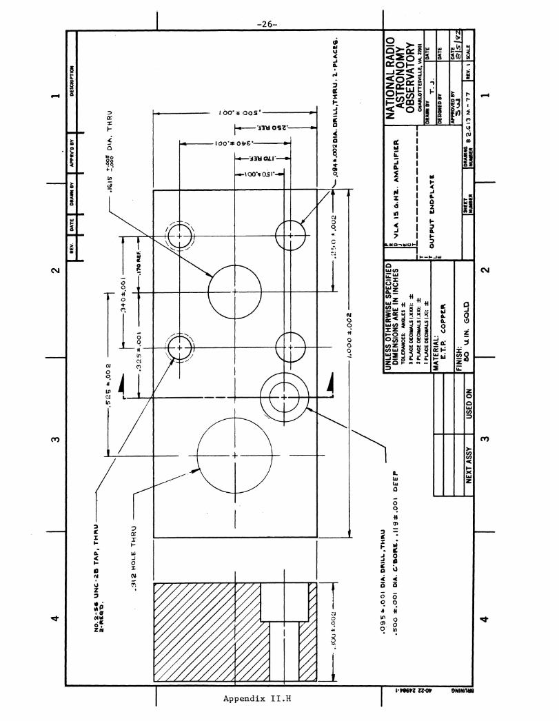
6 U
NC
-25
TAP
TH
RU
, 2-
PLA
CE
S.1
70 R
EF. -
01
.340
±.0
01
DA
TED
ESIG
NED
BY
I
REV
.D
ATE
I
DRA
WN
BY
APP
RV
*0 B
YD
ESCR
IPTI
ON
1.00
0 4.
.002
H-2
6• 0
.„0
02
.1e1
5" :T
OO
DIA
. H R
U.
.094
t.00
2 D
IA. D
R1L
L. •
THR
U2-
PLA
CE
S
r..
..■
••■
■■
10
0 .
001
UN
LESS
OTH
ERW
ISE
SPEC
IFIE
DD
IMEN
SIO
NS
ARE
IN I
NCH
EST
OL
ER
AN
CE
S: A
NG
LE
S ±
3 PL
AC
E D
ECIM
ALS
(.X
XX
):2
PLA
CE
DEC
IMA
LS (.
XX
):1
PLA
CE
DEC
IMA
LS (.
)0: •
±
MAT
ERIA
L:E.T
.P. CO
PPER
lP
It 0 V
LA I
SG.H
Z. A
MPL
IF1E
IRJ E T
t IN
PUT E
ND
PLATE
NAT
ION
AL R
ADIO
AST
RO
NO
MY
OBS
ERVATO
RY
CH
AR
LOTT
ESV
ILLE
, VA
. 229
01' D
RAW
N BY
T. J
.
NM.
ON
O.
1111
1,11
1•. •
1111
10 1
1011
•0 M
ON
O IM
MO
MIN
N =
1=1,
01.■
OM
NI
DA
TE
43
21
NEX
T AS
SYU
SED
ON
FINI
SH: 130
u. IN
. G
OLD
SHEE
TDR
AWIN
GN
UM
BER
NU
MB
ER Ø
,R
EV. S
CA
LE
' APP
RO
VE!
) BY
CV
DA
TEri
sir
110•
1111
0•M
MO
tt
43
1
443
2I R
EV
. 1
DA
TE
I D
RA
WN
BY
APP
ItY
'D B
Y I
DES
CRIP
TIO
N
■•■
•■•
I I MI •
I I I I
I II NM
1 NM
.200
&.0
06•■•
•■•■■
■■■
■■
■■•
■••■
•• ••
••••
■■•■
JAC
K ,
OM
NI
- SP
EC
TR
A M
OO
. 2.0
4 C
CP
AR
T N
O. 2
.052
- 1
201-
00
OR
S0L
1TR
ON
Z95
0- G
OG
1 .
NEX
T AS
SYU
SED
ON
3
UN
LESS
OTH
ERW
ISE
SPEC
IFIE
DD
IMEN
SIO
NS
ARE
IN I
NCH
EST
OL
ER
AN
CE
S: A
NG
LE
S ±
3 PL
AC
E D
ECIM
ALS
(.X
XX
):2
PLA
CE
DEC
IMA
LS (.
XX
):1
PLA
CE
DEC
IMA
LS (.
X):
MAT
ERIA
L:
FINI
SH:
0 V
LA
15
G.H
Z. A
MP
LIF
IER
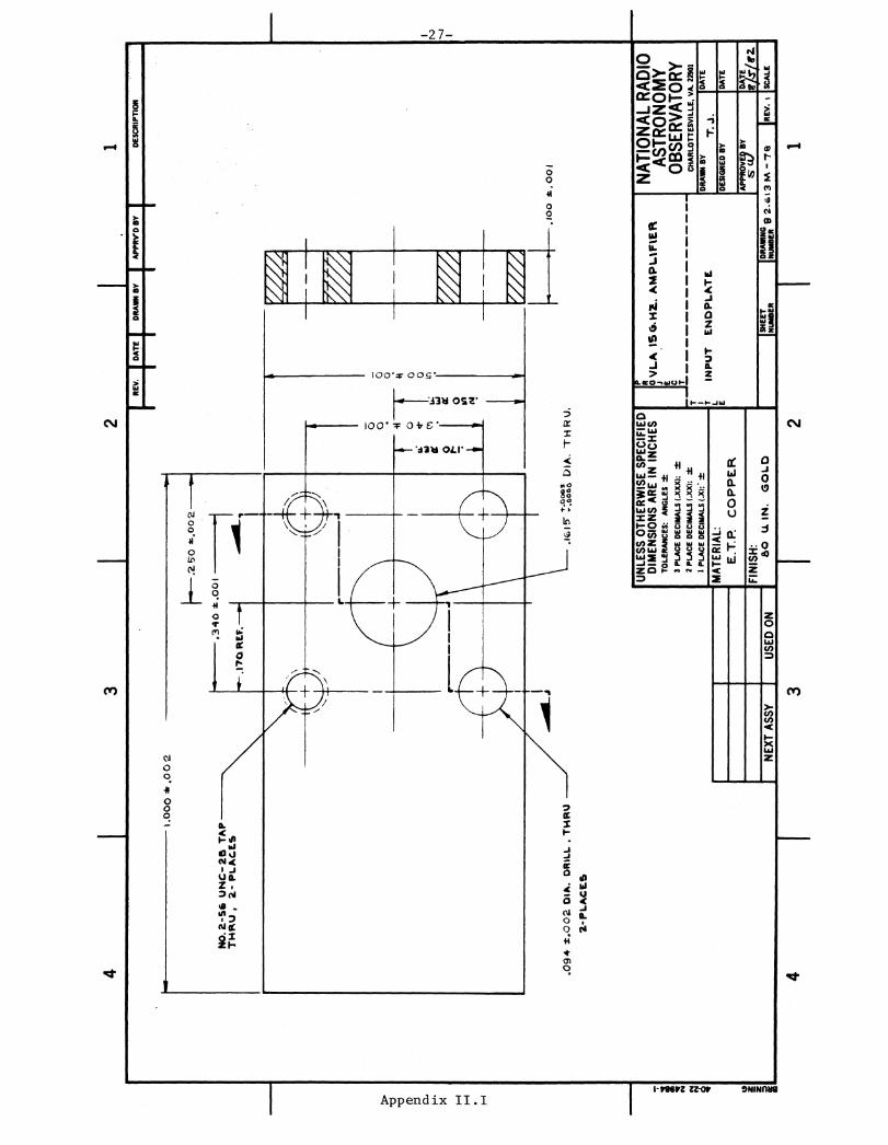
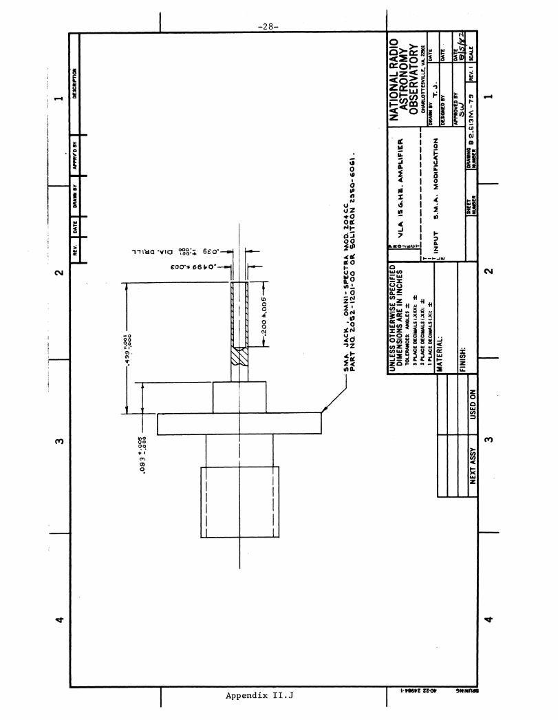
INPU
T S
.M.A
. M
OD
IFIC
ATIO
N
21
NAT
ION
AL R
ADIO
AST
RO
NO
MY
OBS
ERVATO
RY
CH
AR
LOTT
ESV
ILLE
, VA
. 229
01
' APP
RO
VED
BY
DRA
WN
BYT
. J.
DES
IGN
ED B
Y
DA
TE
DA
TE
DA
TE
SCA
LEIS
HE
ET
'DR
AIN
ING
9 2
.613M
-79
IRE
V.
I[N
UM
BER
MA
WR
4I
3RE
V.DA
TEDR
AWN
BYAP
PRV'
D B
Y I
DESC
RIPT
ION
.5•9
9 .0
01
2 9
3 ."(
.;)
Col O• 0
0. 41
00
00
co
r,(
• ')
0 •-t-
t
SM
A J
AC
K ,
OM
NI-
SP
EC
TR
A M
OD
. 104
CC
•P
AR
T N
O.
10S
t-1101-0
0 O
R S
OL
ITR
ON
2.
0-4
0I I
UN
LESS
OTH
ERW
ISE
SPEC
IFIE
DD
IMEN
SIO
NS
ARE
IN I
NCH
ESTO
LERN
ICES
: AN
GLE
S ±
3 PL
ACE
DECI
MAL
S (.
XXX)
:2
PLAC
E D
ECIM
ALS
(.X/
0: ±
1 PL
ACE
DECI
MAL
S (./
0:
o v
LA
156.1
11 A
MP
LIF
IER
=N
D M
INIM
NIN
O 4
WD
= •
1101110 I
MP
MO
M M
EM
41
11
•MIP
MIN
D N
IRO
ON
O 1
1111
11
NAT
ION
AL R
ADIO
AST
RO
NO
MY
OBS
ERVATO
RY
CHAR
LOTT
ESVI
LLE,
VA.
229
01DR
AWN
BYDA
TE
MAT
ERIA
L:O
UT
PU
T b
.M.A
.. M
OD
IFIC
AT
ION
DESI
GNED
BY
T. J.
DATE
FIN
ISH
:N
EXT
ASSY
USE
D O
N
APPR
OVE
D BY
DAT
E$
giS
iga
ISH
EET
1DRA
INN
G B
2.613 NA
IR E
V. 1
SCA
LE'N
UMBE
RNU
MBE
R
3I
21
APP
RO
VED
BY
DATE
REV
.SCALE
REV
.D
ATE
DRA
WN
BY
AP
PR
V'D
BY
DES
CRIP
TIO
N
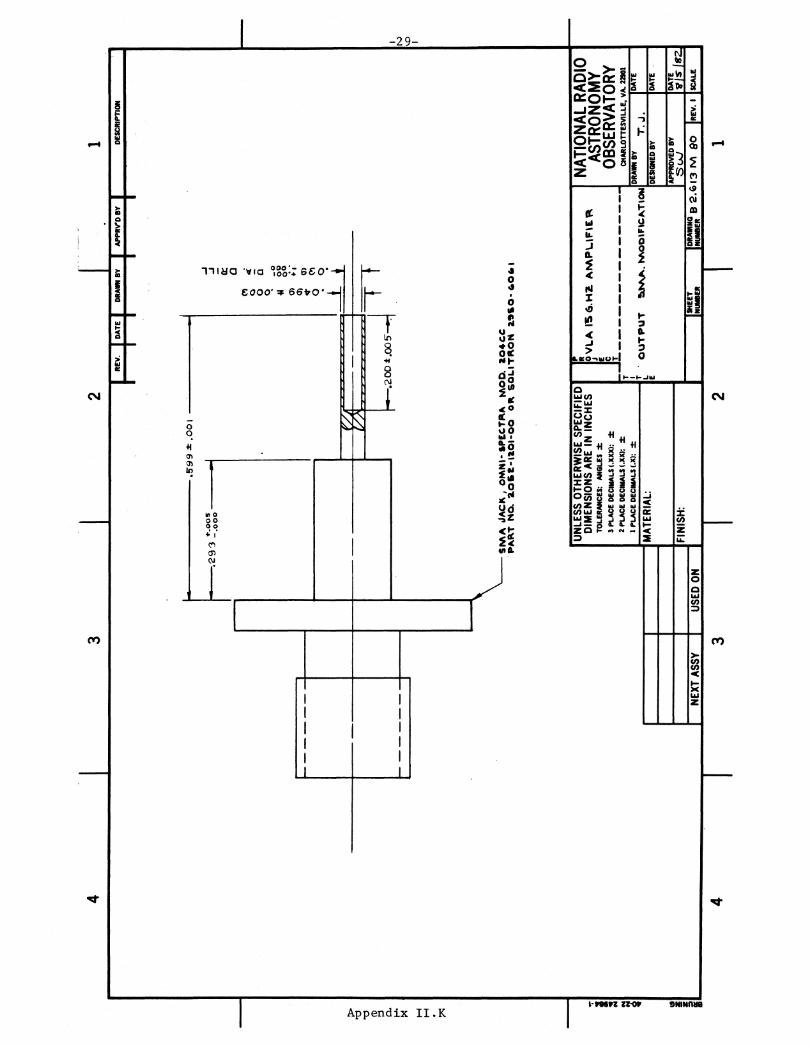
SM
A J
ACK O
MN
I- S
PECTR -
IM
OO
'204
CCPA
RT
NO
. 20
52 -
1201
- 00
.392
OR S
0L1T
R0N
295
0-60
Q 1
,I
MO
DIF
Y A
S I
ND
ICATED
0
i
P R 0 V
IA
IS
GH
Z A
MP
LIF
IER
J E
1 M
OU
NT
I N
G P
LA
TE
WIT
H
E O
UT
PU
T T
RA
NS
ITIO
N
NA
TIO
NA
L R
AD
IOA
ST
RO
NO
MY
OB
SE
RV
AT
OR
YCH
ARLO
TTES
VIL
LE,
VA.
2290
1
DRA
WN
bDA
TEow
o4
3/8
3D
ESIG
NED
BY
DATE
MAT
ERIA
L:
UNLE
SS O
THER
WIS
E SP
ECIF
IED
DIM
ENSI
ONS
ARE
IN IN
CHES
TO
LERAN
CES:
AN
GLE
S ±
3 P
LACE D
ECIM
ALS
(.X
XX):
± .
005
2 PL
ACE
DEC
IMALS
(.X
X):
1 PL
ACE
DEC
IMALS
(.X
):
FINI
SH:
NEXT
ASS
YUS
ED O
NSH
EET
DRA
WIN
GN
UM
BER
NU
MBER
2.6
'3 M
91
3.
9 7
0
DE
TAIL
PA
RT
IO
NLY
— (
TO
P)
SCALE
;
I NO
TES
I 1. D
IMEN
SION
S ARE
Aeo
uA
CEN
TERLI
NE
UN
LESS
II N
DIC
ATE
D'2
.040
r 15
0
.198
±.0
02H
--
SE
CT
ION
AA
5C
AL
E 4
43
AS
SE
MB
LY
-(F
RO
NT
)SALE 2
:1
v1,
PART
I.I
Till
, I
II
:±D 4
4J
Cr
0 (‘!
1C,
I 40
oacP
: S,D
E.4
PLA
CES
j75 D
IAT
H2
PLACES
2-.5C T
HRki —
C.‘
SIN
K B
ACK
5 3D
E.'
5 Pt
AL
ES
,..1T
2 RE
F
r. •
.4.E.C
,
Rt:
6-32
\CL
.EAR
\4
PLAC
ES
4
BRAS
S .CO
LLAR
OD
122
I.
0.
.05
sN
‘e s
oL
oE
k
r ."0
A
20
E2
so
LD
ER
—P
EG
. G
O- 40 S
OL
VE
R
AS
SE
MB
LI
ED
-"S
IDE
)S
CA
LE
2:1
SO
ME
HID
DE
N L
INE
S °
MIT
TE
L)
FO
R C
LA
RIT
Y
N
.. A