Embed Size (px)
Citation preview
NAU8220
Datasheet Revision 2.0 Page 1 of 19
2Vrms Audio Line Driver
1 General Description
The NAU8220 is a high quality 2Vrms analog input and output line driver. This device includes an integrated charge pump enabling true ground referenced inputs and outputs and full 5.6Vpp output levels, while operating from only a single 3.3V positive supply voltage. Additionally, the NAU8220 includes pop/click elimination features and high immunity to power supply and other system noise. This enables fast and efficient system integration while minimizing external component costs. The NAU8220 is specified for operation from -40°C to +85°C, It is packaged in a cost-effective and space-saving 14-lead SOP and TSSOP packages.
2 Features
Operating voltage: 3.0-3.6V Full 2Vrms output using only 3.3Vdc supply True Ground Referenced analog outputs Low cost, small footprint package Automatic pop/click elimination and output muting for power-on 108dB SNR A-weighted performance >90dB THD+N 114dB Mute Attenuation < 1mV Output Offset 110dB channel separation at 1kHz Low external parts count High system noise immunity Packages: Pb free 14-pin SOP and TSSOP Operating temperature range: -40 to +85°C ±8 kV HBM protection on line outputs
NAU8220
Datasheet Revision 2.0 Page 2 of 19
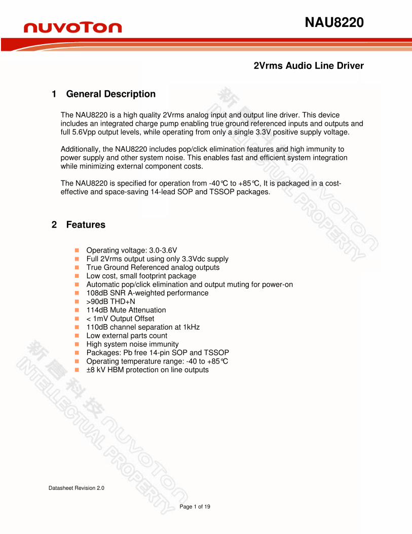
3 Block diagram
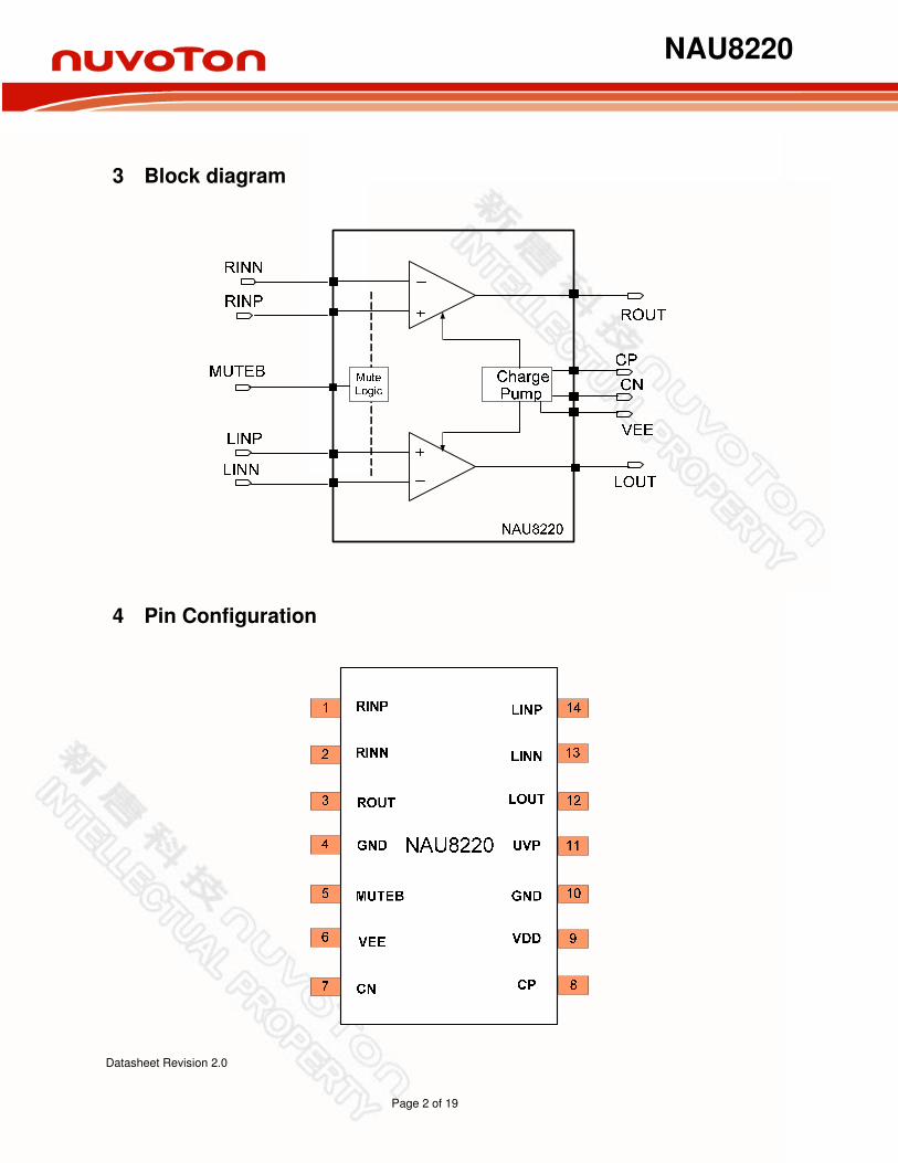
4 Pin Configuration
NAU8220
Datasheet Revision 2.0 Page 3 of 19
5 Pin Description
Pin No. Pin Name Type Description
1 RINP AI Right Channel Positive Input
2 RINN AI Right Channel Negative Input
3 ROUT O Right Channel Line Output
4 GND P Ground
5 MUTEB I Mute Bar
6 VEE IO Charge Pump Decoupling Output (Negative Voltage)
7 CN IO Charge Pump Capacitor Negative Node
8 CP IO Charge Pump Capacitor Positive Node
9 VDD P Positive Voltage Supply
10 GND P Ground
11 UVP I Under Voltage Protection
12 LOUT O Left Channel Line Output
13 LINN AI Left Channel Negative Input
14 LINP AI Left Channel Positive Input
Table 1 Pin Description
NAU8220
Datasheet Revision 2.0 Page 4 of 19
6 Table of Contents
1 GENERAL DESCRIPTION ................................................................................................................................. 1
2 FEATURES ......................................................................................................................................................... 1
3 BLOCK DIAGRAM ............................................................................................................................................. 2
4 PIN CONFIGURATION ....................................................................................................................................... 2
5 PIN DESCRIPTION ............................................................................................................................................. 3
6 TABLE OF CONTENTS ...................................................................................................................................... 4
7 ABSOLUTE MAXIMUM RATINGS ..................................................................................................................... 5
8 RECOMMENDED OPERATING CONDITIONS .................................................................................................. 5
9 ELECTRICAL CHARACTERISTICS .................................................................................................................. 6
10 FUNCTIONAL DESCRIPTION ............................................................................................................................ 7
11 AMPLIFIER CIRCUITS ....................................................................................................................................... 8
12 LOW PASS FILTER CIRCUIT ............................................................................................................................ 9
13 TYPICAL APPLICATION DIAGRAM ................................................................................................................ 12
14 TYPICAL CHARACTERISTICS ........................................................................................................................ 14
15 PACKAGE SPECIFICATION ............................................................................................................................ 17
15.1 SOP-14 Package ....................................................................................................................................... 17
15.2 TSSOP-14 Package (14L 4.4X5.0 MM^2) .................................................................................................. 18
16 ORDERING INFORMATION ............................................................................................................................. 19

NAU8220
Datasheet Revision 2.0 Page 5 of 19
7 Absolute Maximum Ratings
DESCRIPTION SYMBOL CONDITION MINIMUM MAXIMUM UNIT
VDD supply voltage VDD VDD−GND -0.3 +4.0 V
Digital Input Voltage range
DVIN DVIN− GND GND – 0.3 VDD + 0.30 V
Analog Input Voltage AVIN AVIN− VEE VEE – 0.3 VDD + 0.30 V
Operating Temperature
TA -40 +85 °C
Storage Temperature Tst -65 +150 °C CAUTION: Do not operate at or near the maximum ratings listed for extended periods of time. Exposure to such Conditions may adversely influence product reliability and result in failures not covered by warranty. Follow IC handling procedures to avoid ESD damage.
8 Recommended Operating Conditions
DESCRIPTION SYMBOL MINIMUM TYPICAL MAXIMUM UNIT
Supply voltage VDD 3.0 3.3 3.6 V
Ground GND 0 V
NAU8220
Datasheet Revision 2.0 Page 6 of 19
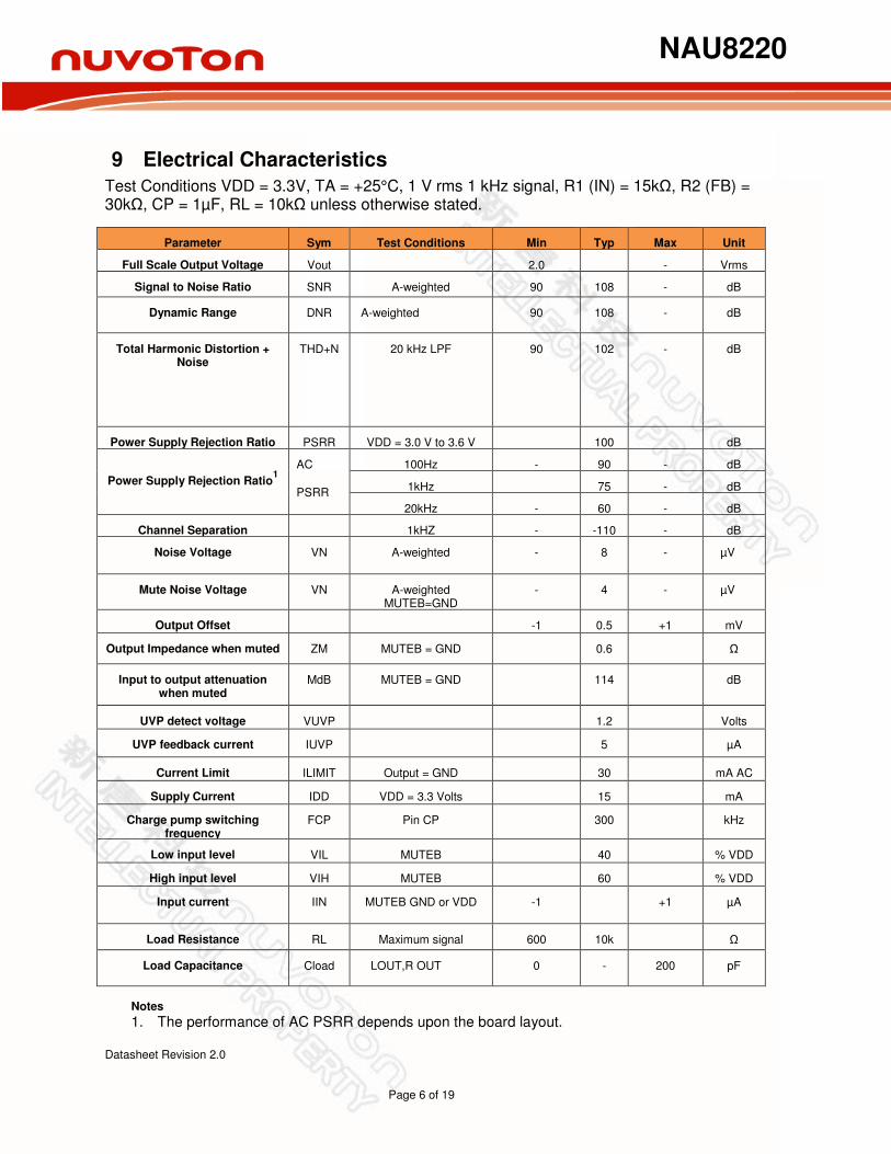
9 Electrical Characteristics
Test Conditions VDD = 3.3V, TA = +25°C, 1 V rms 1 kHz signal, R1 (IN) = 15kΩ, R2 (FB) = 30kΩ, CP = 1µF, RL = 10kΩ unless otherwise stated.
Parameter Sym Test Conditions Min Typ Max Unit
Full Scale Output Voltage Vout 2.0 - Vrms
Signal to Noise Ratio SNR A-weighted 90 108 - dB
Dynamic Range DNR A-weighted 90 108 - dB
Total Harmonic Distortion + Noise
THD+N
20 kHz LPF
90
102
-
dB
Power Supply Rejection Ratio PSRR VDD = 3.0 V to 3.6 V 100 dB
Power Supply Rejection Ratio1
AC
PSRR
100Hz - 90 - dB
1kHz 75 - dB
20kHz - 60 - dB
Channel Separation 1kHZ - -110 - dB
Noise Voltage VN A-weighted - 8 - µV
Mute Noise Voltage VN A-weighted MUTEB=GND
- 4 - µV
Output Offset -1 0.5 +1 mV
Output Impedance when muted ZM MUTEB = GND 0.6 Ω
Input to output attenuation when muted
MdB MUTEB = GND 114 dB
UVP detect voltage VUVP 1.2 Volts
UVP feedback current IUVP 5 µA
Current Limit ILIMIT Output = GND 30 mA AC
Supply Current IDD VDD = 3.3 Volts 15 mA
Charge pump switching frequency
FCP Pin CP 300 kHz
Low input level VIL MUTEB 40 % VDD
High input level VIH MUTEB 60 % VDD
Input current IIN MUTEB GND or VDD -1 +1 µA
Load Resistance RL Maximum signal 600 10k Ω
Load Capacitance Cload LOUT,R OUT 0 - 200 pF
Notes
1. The performance of AC PSRR depends upon the board layout.
NAU8220
Datasheet Revision 2.0 Page 7 of 19
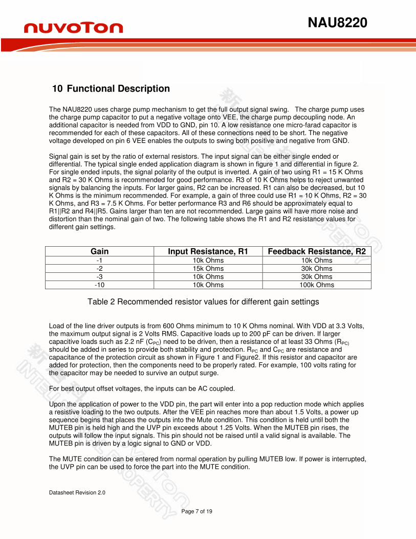
10 Functional Description
The NAU8220 uses charge pump mechanism to get the full output signal swing. The charge pump uses the charge pump capacitor to put a negative voltage onto VEE, the charge pump decoupling node. An additional capacitor is needed from VDD to GND, pin 10. A low resistance one micro-farad capacitor is recommended for each of these capacitors. All of these connections need to be short. The negative voltage developed on pin 6 VEE enables the outputs to swing both positive and negative from GND. Signal gain is set by the ratio of external resistors. The input signal can be either single ended or differential. The typical single ended application diagram is shown in figure 1 and differential in figure 2. For single ended inputs, the signal polarity of the output is inverted. A gain of two using R1 = 15 K Ohms and R2 = 30 K Ohms is recommended for good performance. R3 of 10 K Ohms helps to reject unwanted signals by balancing the inputs. For larger gains, R2 can be increased. R1 can also be decreased, but 10 K Ohms is the minimum recommended. For example, a gain of three could use R1 = 10 K Ohms, R2 = 30 K Ohms, and R3 = 7.5 K Ohms. For better performance R3 and R6 should be approximately equal to R1||R2 and R4||R5. Gains larger than ten are not recommended. Large gains will have more noise and distortion than the nominal gain of two. The following table shows the R1 and R2 resistance values for different gain settings.
Gain Input Resistance, R1 Feedback Resistance, R2 -1 10k Ohms 10k Ohms
-2 15k Ohms 30k Ohms
-3 10k Ohms 30k Ohms
-10 10k Ohms 100k Ohms
Table 2 Recommended resistor values for different gain settings Load of the line driver outputs is from 600 Ohms minimum to 10 K Ohms nominal. With VDD at 3.3 Volts, the maximum output signal is 2 Volts RMS. Capacitive loads up to 200 pF can be driven. If larger capacitive loads such as 2.2 nF (CPC) need to be driven, then a resistance of at least 33 Ohms (RPC) should be added in series to provide both stability and protection. RPC and CPC are resistance and capacitance of the protection circuit as shown in Figure 1 and Figure2. If this resistor and capacitor are added for protection, then the components need to be properly rated. For example, 100 volts rating for the capacitor may be needed to survive an output surge. For best output offset voltages, the inputs can be AC coupled. Upon the application of power to the VDD pin, the part will enter into a pop reduction mode which applies a resistive loading to the two outputs. After the VEE pin reaches more than about 1.5 Volts, a power up sequence begins that places the outputs into the Mute condition. This condition is held until both the MUTEB pin is held high and the UVP pin exceeds about 1.25 Volts. When the MUTEB pin rises, the outputs will follow the input signals. This pin should not be raised until a valid signal is available. The MUTEB pin is driven by a logic signal to GND or VDD. The MUTE condition can be entered from normal operation by pulling MUTEB low. If power is interrupted, the UVP pin can be used to force the part into the MUTE condition.
NAU8220
Datasheet Revision 2.0 Page 8 of 19
The UVP pin can force the part into the Mute condition when the power supply voltage drops below the desired voltage. If this function is not needed, the UVP pin should be connected to VDD. Feed back is provided by a nominal 5 µA current developed across the external resistors applied. The turn on voltage sets the ratio of R11 and R12 compared to the internal 1.22 Volt reference. The formula for turn ON voltage is VON = 1.22V * (R11 + R12)/R11 and the formula for the turn off voltage is VOFF= VON - (5uA * R12). For example, for a turn on voltage of 3.0 Volts and a turn off voltage of 2.5 volts, the calculated resistors are R11 = 68.5kΩ and R12 = 100kΩ, or using standard values, R11 = 68kΩ and R12 = 100kΩ. Important note: When using a LDO, the turn-on and turn-off voltages for the UVP should be set higher than the sum of 3.3V and the minimum required voltage drop across the LDO, to ensure proper operation.
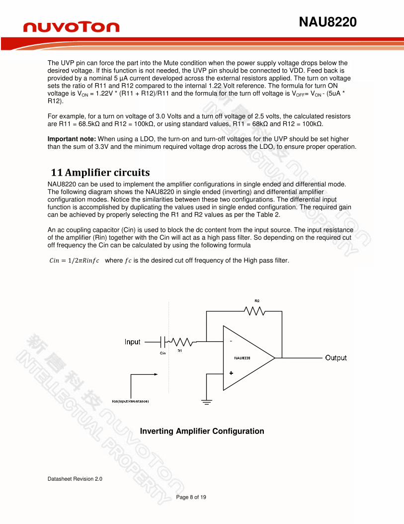
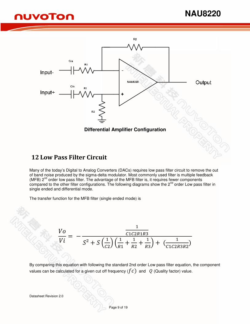
11 Amplifier circuits NAU8220 can be used to implement the amplifier configurations in single ended and differential mode. The following diagram shows the NAU8220 in single ended (inverting) and differential amplifier configuration modes. Notice the similarities between these two configurations. The differential input function is accomplished by duplicating the values used in single ended configuration. The required gain can be achieved by properly selecting the R1 and R2 values as per the Table 2. An ac coupling capacitor (Cin) is used to block the dc content from the input source. The input resistance of the amplifier (Rin) together with the Cin will act as a high pass filter. So depending on the required cut off frequency the Cin can be calculated by using the following formula 1/2 where is the desired cut off frequency of the High pass filter.
Inverting Amplifier Configuration
NAU8220
Datasheet Revision 2.0 Page 9 of 19
Differential Amplifier Configuration
12 Low Pass Filter Circuit Many of the today’s Digital to Analog Converters (DACs) requires low pass filter circuit to remove the out of band noise produced by the sigma-delta modulator. Most commonly used filter is multiple feedback (MFB) 2
nd order low pass filter. The advantage of the MFB filter is, it requires fewer components
compared to the other filter configurations. The following diagrams show the 2nd
order Low pass filter in single ended and differential mode. The transfer function for the MFB filter (single ended mode) is
²
By comparing this equation with following the standard 2nd order Low pass filter equation, the component
values can be calculated for a given cut off frequency ( and (Quality factor) value.

NAU8220
Datasheet Revision 2.0 Page 10 of 19
2 22 2²
Where !"# " $ 1/2% &'( $ "
)
Single ended 2nd order Low pass filter
Example1: Design a second order single ended MFB Low pass filter with following specifications. Cut off Frequency = 50 kHz, Quality factor, Q= 0.707 and Gain, K = -2. Step 1: Find R1 and R2 depending on the gain. By assuming R1 = 10kOhms and using the equation
the value of the R2 = 20kOhms.

NAU8220
Datasheet Revision 2.0 Page 11 of 19
Step2: Using the equation *+,-
, Calculate R3 by assuming C2 = 1000pF
R3 = 3.3kOhms
Step3: Using the equation2 , the C1 = 150pF
Example2: Design a second order differential mode MFB Low pass filter with following specifications. Cut off Frequency = 50 kHz, Quality factor, Q= 0.707 and Gain, K = -2. The differential mode configuration can be achieved by duplicating the above example 1 values except the C2. The C2 value in this configuration is half of the value of the single ended configuration.
Differential 2nd order Low pass filter
NAU8220
Datasheet Revision 2.0 Page 12 of 19
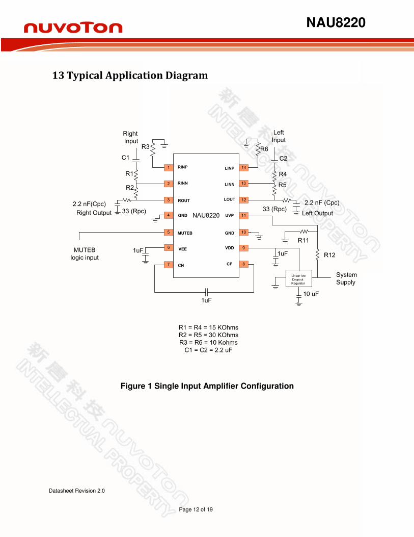
13 Typical Application Diagram
MUTEB
logic input
Right Output NAU8220
1
2
3
4
5
6
7
14
13
12
11
10
9
8
RINP
RINN
ROUT
GND
MUTEB
VEE
CN
LINP
LINN
LOUT
UVP
GND
VDD
CP
Right
Input
Left
Input
R6R3
C1 C2
R1
R2
R4
R5
33 (Rpc) 33 (Rpc)2.2 nF (Cpc)2.2 nF(Cpc)
1uF1uF
1uF
Left Output
R11
R12
10 uF
System
Supply
Linear low
Dropout
Regulator
R1 = R4 = 15 KOhms
R2 = R5 = 30 KOhms
R3 = R6 = 10 Kohms
C1 = C2 = 2.2 uF
Figure 1 Single Input Amplifier Configuration

NAU8220
Datasheet Revision 2.0 Page 13 of 19
NAU8220
1
2
3
4
5
6
7
14
13
12
11
10
9
8
RINP
RINN
ROUT
GND
MUTEB
VEE
CN
LINP
LINN
LOUT
UVP
GND
VDD
CP
Right
Input
- +
Left
Input
+ -
R7R3
C1 C4
R1
R2
R5
R6
33 (Rpc) 33 (Rpc) 2.2 nF (Cpc)2.2 nF (Cpc)
1uF1uF
1uF
Right Output Left Output
R11
10 uF
Linear low
Dropout
Regulator
R1 = R3 = R5 = R7= 15 KOhms
R2 = R4 = R6 = R8 = 30 KOhms
C1 = C2 = C3 = C4 = 2.2 uF
C2
R4 R8
R12
System
Supply
MUTEB Logic
Input
C3
Figure 2 Differential Input Amplifier Configuration

NAU8220
Datasheet Revision 2.0 Page 14 of 19
14 Typical Characteristics Test Conditions VDD = 3.3V, TA = +25°C, 1kHz signal, R1 (IN) = 15kΩ, R2 (FB) = 30kΩ, CP = 1µF, RL = 10kΩ, CPC = 2200pF, RPC= 33 Ohms unless otherwise stated.
Total Harmonic Distortion + Noise Vs Frequency
Total Harmonic Distortion + Noise Vs Output Voltage
0
0.002
0.004
0.006
0.008
0.01
10 100 1000 10000 100000
TH
D+
N (
%)
Frequency (Hz)
RL = 10k Ohms
2V RMS
1V RMS
0
0.002
0.004
0.006
0.008
0.01
10 100 1000 10000 100000
TH
D+
N (
%)
Frequency (Hz)
RL= 600 Ohms With out RPC and CPC
2V RMS
1V RMS
0.0001
0.001
0.01
0.1
1
10
0 1 2 3
TH
D+
N (
%)
Vout RMS (V)
RL=10k Ohms, F = 100 Hz
0.0001
0.001
0.01
0.1
1
10
0 1 2 3
TH
D+
N (
%)
Vout RMS (V)
RL=600 Ohms, F= 100 Hz

NAU8220
Datasheet Revision 2.0 Page 15 of 19
0.0001
0.001
0.01
0.1
1
10
0 1 2 3
TH
D+
N (
%)
Vout RMS (V)
RL=10k Ohms, F = 1kHz
0.0001
0.001
0.01
0.1
1
10
0 1 2 3
TH
D+
N (
%)
Vout RMS (V)
RL=600 Ohms, F = 1kHz
0.0001
0.001
0.01
0.1
1
10
0 1 2 3
TH
D+
N (
%)
Vout RMS (V)
RL=10k Ohms, F = 10kHz
0.0001
0.001
0.01
0.1
1
10
0 1 2 3
TH
D+
N (
%)
Vout RMS (V)
RL=600 Ohms, F = 10kHz
NAU8220
Datasheet Revision 2.0 Page 16 of 19
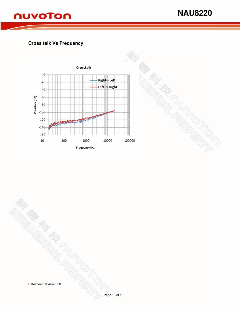
Cross talk Vs Frequency
-160
-140
-120
-100
-80
-60
-40
-20
0
10 100 1000 10000 100000
Cro
ssta
lk (
dB
)
Frequency (Hz)
Crosstalk
Right->Left
Left -> Right
NAU8220
Datasheet Revision 2.0 Page 17 of 19
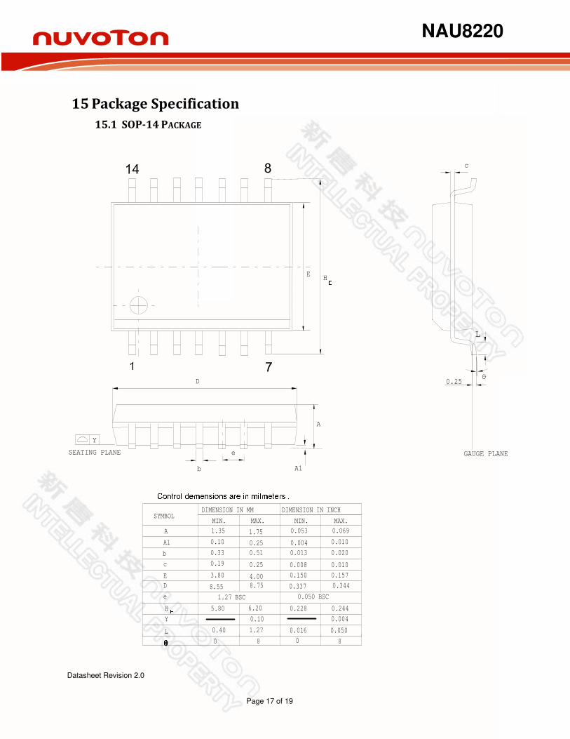
15 Package Specification
15.1 SOP-14 PACKAGE
SEATING PLANE
L
O
c
0.25
GAUGE PLANEControl demensions are in milmeters .4.00
0.25
0.51
0.25
E
c
b
A1
3.80
0.19
0.33
0.10
0.157
0.010
0.020
0.010
0.150
0.008
0.013
0.004
MAX.
DIMENSION IN MM
1.75A
SYMBOLMIN.
1.35
DIMENSION IN INCH
0.069
MIN.
0.053
MAX.
1.27
0.10
6.20
L
θθθθ
Y
H
0 8
0.40
5.80
e 1.27 BSC
0.050
0.004
0.244
0
0.016
0.228
8
0.050 BSCED 8.55 8.75 0.337 0.344
EH E
1
14 8
7
A1
A
e
b
D
Y
NAU8220
Datasheet Revision 2.0 Page 18 of 19
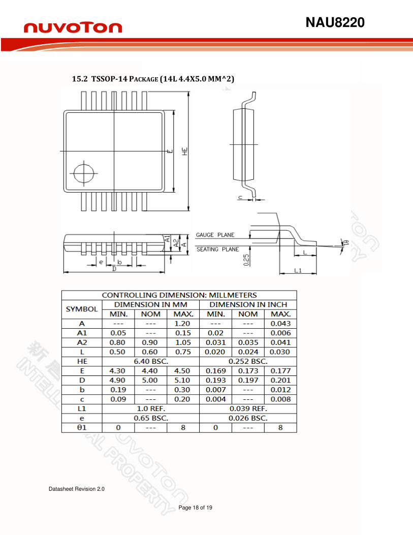
15.2 TSSOP-14 PACKAGE (14L 4.4X5.0 MM^2)
NAU8220
Datasheet Revision 2.0 Page 19 of 19
16 Ordering Information Nuvoton Part Number Description
NAU8220_ _
Version History
VERSION DATE PAGE DESCRIPTION
1.8 Feb 2012 9 Added application circuit diagram with differential
configuration.
1.9 March 2012 14 Added TSSOP package dimensions information
2.0 June, 2012 6,8-
11,12,13
1. Corrected Application circuit diagram. Changed value of input DC blocking capacitors to 2.2 uF.
2.Added Load resistance and Load capacitance column in the Electrical characteristics table
3.Added amplifier circuit and 2nd
order LPF circuit
Important Notice
Nuvoton products are not designed, intended, authorized or warranted for use as components in systems or equipment intended for surgical implantation, atomic energy control instruments, airplane or spaceship instruments, transportation instruments, traffic signal instruments, combustion control instruments, or for other applications intended to support or sustain life. Furthermore, Nuvoton products are not intended for applications wherein failure of Nuvoton products could result or lead to a situation wherein personal injury, death or severe property or environmental damage could occur. Nuvoton customers using or selling these products for use in such applications do so at their own risk and agree to fully indemnify Nuvoton for any damages resulting from such improper use or sales.
Package Type:
S = 14-Pin SOP Package
W = 14-Pin TSSOP Package
Package Material:
G = Pb-free Package / Green


![Data Sheet - RS Components · 2019. 10. 17. · 2 Package Dimensions Absolute Maximum Ratings Supply Voltage, VDD to Ground[1]-0.3 V to 7.0 V Operating Voltage, VDD to Ground[2] 5.5](https://img.pdfslide.net/doc/110x75/6078d6892678e0607178fc1e/data-sheet-rs-components-2019-10-17-2-package-dimensions-absolute-maximum.jpg)