Embed Size (px)
Citation preview
7/24/2019 NCP349-D
http://slidepdf.com/reader/full/ncp349-d 1/12
© Semiconductor Components Industries, LLC, 2012
September, 2012− Rev. 3
1 Publication Order Number:
NCP349/D
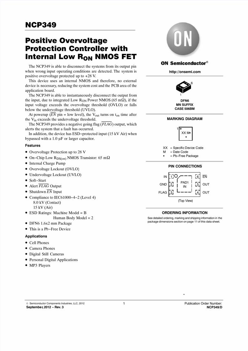
NCP349
Positive OvervoltageProtection Controller withInternal Low RON NMOS FET
The NCP349 is able to disconnect the systems from its output pin
when wrong input operating conditions are detected. The system ispositive overvoltage protected up to +28 V.
This device uses an internal NMOS and therefore, no externaldevice is necessary, reducing the system cost and the PCB area of the
application board.The NCP349 is able to instantaneously disconnect the output from
the input, due to integrated Low RON Power NMOS (65 m), if theinput voltage exceeds the overvoltage threshold (OVLO) or falls
below the undervoltage threshold (UVLO). At powerup ( EN pin = low level), the Vout turns on ton time after
the Vin exceeds the undervoltage threshold.
The NCP349 provides a negative going flag ( FLAG) output, whichalerts the system that a fault has occurred.
In addition, the device has ESD−protected input (15 kV Air) whenbypassed with a 1.0 F or larger capacitor.
Features
• Overvoltage Protection up to 28 V
• On−Chip Low RDS(on) NMOS Transistor: 65 m
• Internal Charge Pump
• Overvoltage Lockout (OVLO)
• Undervoltage Lockout (UVLO)
• Soft−Start
• Alert FLAG Output
• Shutdown EN Input
• Compliance to IEC61000−4−2 (Level 4)
8.0 kV (Contact)
15 kV (Air)
• ESD Ratings: Machine Model = B
Human Body Model = 2
• DFN6 1.6x2 mm Package
• This is a Pb−Free Device
Applications
• Cell Phones
• Camera Phones
• Digital Still Cameras
• Personal Digital Applications
• MP3 Players
DFN6
MN SUFFIX
CASE 506BM
PIN CONNECTIONS
http://onsemi.com
MARKING DIAGRAM
XX = Specific Device Code
M = Date Code
= Pb−Free Package
(Top View)
1
FLAG OUT
GND OUT
IN EN
2
3
6
5
4
PAD1
IN
ORDERING INFORMATION
See detailed ordering, marking and shipping information in the
package dimensions section on page 11 of this data sheet.
1
6
XX M
1
7/24/2019 NCP349-D
http://slidepdf.com/reader/full/ncp349-d 2/12
NCP349
http://onsemi.com
2
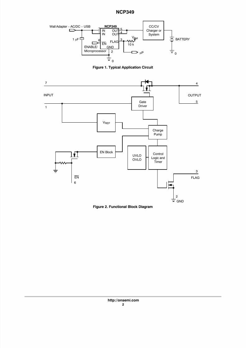
Figure 1. Typical Application Circuit
IN7
OUT 5
GND
2
6 3
IN1
OUT4
NCP349
0
1 F
10 k
Wall Adapter − AC/DC − USB
BATTERY
0
CC/CV
Charger or
SystemVBat
ENABLE/
Microprocessor
ENFLAG
P
Figure 2. Functional Block Diagram
INPUT OUTPUT
UVLO
OVLO
Gate
Driver
FLAGEN
EN Block
VREF
Charge
Pump
Control
Logic and
Timer
GND
7
1
6
2
3
5
4
7/24/2019 NCP349-D
http://slidepdf.com/reader/full/ncp349-d 3/12
NCP349
http://onsemi.com
3
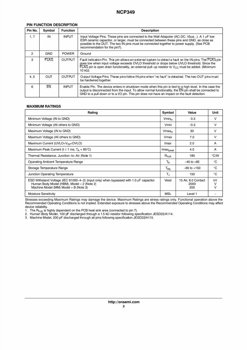
PIN FUNCTION DESCRIPTION
Pin No. Symbol Function Description
1, 7 IN INPUT Input Voltage Pins. These pins are connected to the Wall Adapoter (AC−DC, Vbus ..). A 1 F lowESR ceramic capacitor, or larger, must be connected between these pins and GND, as close aspossible to the DUT. The two IN pins must be connected together to power supply. (See PCBrecommendation for the pin7).
2 GND POWER Ground
3 FLAG OUTPUT Fault Indication Pin. This pin allows an external system to detect a fault on the IN pins. The FLAG pingoes low when input voltage exceeds OVLO threshold or drops below UVLO threshold. Since theFLAG pin is open drain functionality, an external pull−up resistor to VCC must be added. (Minimum10 k).
4, 5 OUT OUTPUT Output Voltage Pins. These pins follow IN pins when “no fault” is detected. The two OUT pins mustbe hardwired together.
6 EN INPUT Enable Pin. The device enters in shutdown mode when this pin is tied to a high level. In this case theoutput is disconnected from the input. To allow normal functionality, the EN pin shall be connected toGND to a pull down or to a I/O pin. This pin does not have an impact on the fault detection.
MAXIMUM RATINGS
Rating Symbol Value Unit
Minimum Voltage (IN to GND) Vminin −0.3 V
Minimum Voltage (All others to GND) Vmin −0.3 V
Maximum Voltage (IN to GND) Vmaxin 30 V
Maximum Voltage (All others to GND) Vmax 7.0 V
Maximum Current (UVLO<VIN<OVLO) Imax 2.0 A
Maximum Peak Current (t ≤ 1 ms, T A = 85°C) Imaxpeak 4.0 A
Thermal Resistance, Junction−to− Air (Note 1) RJA 180 °C/W
Operating Ambient Temperature Range T A −40 to +85 °C
Storage Temperature Range Tstg −65 to +150 °C
Junction Operating Temperature TJ 150 °C
ESD Withstand Voltage (IEC 61000−4−2) (input only) when bypassed with 1.0 F capacitor
Human Body Model (HBM), Model = 2 (Note 2)Machine Model (MM) Model = B (Note 3)
Vesd 15 Air, 8.0 Contact
2000200
kV
VV
Moisture Sensitivity MSL Level 1 −
Stresses exceeding Maximum Ratings may damage the device. Maximum Ratings are stress ratings only. Functional operation above theRecommended Operating Conditions is not implied. Extended exposure to stresses above the Recommended Operating Conditions may affectdevice reliability.1. The RJA is highly dependent on the PCB heat sink area (connected to pin 7).2. Human Body Model, 100 pF discharged through a 1.5 k resistor following specification JESD22/A114.3. Machine Model, 200 pF discharged through all pins following specification JESD22/A115.
7/24/2019 NCP349-D
http://slidepdf.com/reader/full/ncp349-d 4/12
NCP349
http://onsemi.com
4
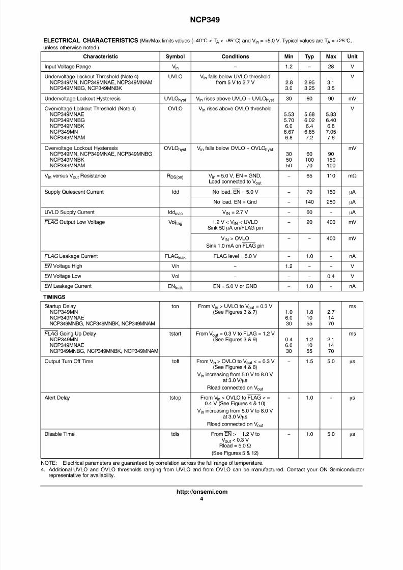
ELECTRICAL CHARACTERISTICS (Min/Max limits values (−40°C < T A < +85°C) and Vin = +5.0 V. Typical values are T A = +25°C,
unless otherwise noted.)
Characteristic Symbol Conditions Min Typ Max Unit
Input Voltage Range Vin − 1.2 − 28 V
Undervoltage Lockout Threshold (Note 4)NCP349MN, NCP349MNAE, NCP349MNAMNCP349MNBG, NCP349MNBK
UVLO Vin falls below UVLO thresholdfrom 5 V to 2.7 V 2.8
3.02.953.25
3.13.5
V
Undervoltage Lockout Hysteresis UVLOhyst Vin rises above UVLO + UVLOhyst 30 60 90 mV
Overvoltage Lockout Threshold (Note 4)NCP349MNAENCP349MNBGNCP349MNBK NCP349MNNCP349MNAM
OVLO Vin rises above OVLO threshold5.535.706.06.676.8
5.686.026.46.857.2
5.836.406.87.057.6
V
Overvoltage Lockout HysteresisNCP349MN, NCP349MNAE, NCP349MNBGNCP349MNBK NCP349MNAM
OVLOhyst Vin falls below OVLO + OVLOhyst305050
6010070
90150100
mV
Vin versus Vout Resistance RDS(on) Vin = 5.0 V, EN = GND,Load connected to Vout
− 65 110 m
Supply Quiescent Current Idd No load. EN = 5.0 V − 70 150 A
No load. EN = Gnd −
140 250 A
UVLO Supply Current Idduvlo VIN = 2.7 V − 60 − A
FLAG Output Low Voltage Volflag 1.2 V < VIN < UVLOSink 50 A on/FLAG pin
− 20 400 mV
VIN > OVLO
Sink 1.0 mA on FLAG pin
− − 400 mV
FLAG Leakage Current FLAGleak FLAG level = 5.0 V − 1.0 − nA
EN Voltage High Vih − 1.2 − − V
EN Voltage Low Vol − − − 0.4 V
EN Leakage Current ENleak EN = 5.0 V or GND − 1.0 − nA
TIMINGSStartup Delay
NCP349MNNCP349MNAENCP349MNBG, NCP349MNBK, NCP349MNAM
ton From Vin > UVLO to Vout = 0.3 V(See Figures 3 & 7) 1.0
6.030
1.81055
2.71470
ms
FLAG Going Up DelayNCP349MNNCP349MNAENCP349MNBG, NCP349MNBK, NCP349MNAM
tstart From Vout = 0.3 V to FLAG = 1.2 V(See Figures 3 & 9) 0.4
6.030
1.21055
2.11470
ms
Output Turn Off Time toff From Vin > OVLO to Vout < = 0.3 V(See Figures 4 & 8)
Vin increasing from 5.0 V to 8.0 Vat 3.0 V/ s
Rload connected on Vout
− 1.5 5.0 s
Alert Delay tstop From Vin > OVLO to FLAG < =0.4 V (See Figures 4 & 10)
Vin increasing from 5.0 V to 8.0 Vat 3.0 V/ s
Rload connected on Vout
−
1.0 −
s
Disable Time tdis From EN > = 1.2 V toVout < 0.3 V
Rload = 5.0
(See Figures 5 & 12)
− 1.0 5.0 s
NOTE: Electrical parameters are guaranteed by correlation across the full range of temperature.
4. Additional UVLO and OVLO thresholds ranging from UVLO and from OVLO can be manufactured. Contact your ON Semiconductorrepresentative for availability.
7/24/2019 NCP349-D
http://slidepdf.com/reader/full/ncp349-d 5/12
NCP349
http://onsemi.com
5
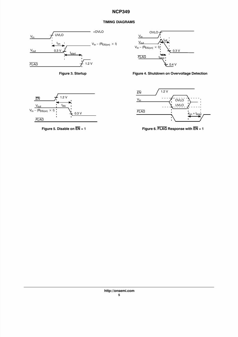
TIMING DIAGRAMS
FLAG
Vout
VinUVLO
ton
0.3 Vtstart
1.2 V
<OVLO
Vin − (RDS(on) I)
FLAG
Vin
EN 1.2 V
OVLO
UVLO
ton + tstart
FLAG
Vout
Vin
OVLO
toff
0.3 V
tstop
0.4 V
Vin − (RDS(on) I)
FLAG
Vout
EN1.2 V
tdis
0.3 VVin − (RDS(on) I)
Figure 3. Startup Figure 4. Shutdown on Overvoltage Detection
Figure 5. Disable on EN = 1 Figure 6. FLAG Response with EN = 1
7/24/2019 NCP349-D
http://slidepdf.com/reader/full/ncp349-d 6/12
NCP349
http://onsemi.com
6
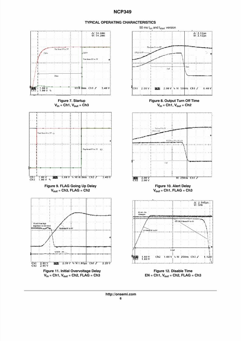
TYPICAL OPERATING CHARACTERISTICS
Figure 7. Startup
V in = Ch1, V out = Ch3
Figure 8. Output Turn Off Time
V in = Ch1, V out = Ch2
Figure 9. FLAG Going Up Delay
V out = Ch3, FLAG = Ch2
Figure 10. Alert Delay
V out = Ch1, FLAG = Ch3
Figure 11. Initial Overvoltage Delay
V in = Ch1, V out = Ch2, FLAG = Ch3
Figure 12. Disable Time
EN = Ch1, V out = Ch2, FLAG = Ch3
50 ms ton and tstart version
7/24/2019 NCP349-D
http://slidepdf.com/reader/full/ncp349-d 7/12
NCP349
http://onsemi.com
7
TYPICAL OPERATING CHARACTERISTICS
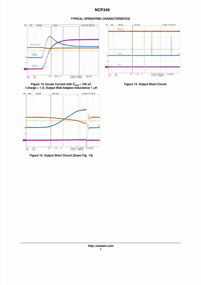
Figure 13. Inrush Current with Cout = 100 F,
I charge = 1 A, Output Wall Adaptor Inductance 1 H
Figure 14. Output Short Circuit
Figure 15. Output Short Circuit (Zoom Fig. 14 )
7/24/2019 NCP349-D
http://slidepdf.com/reader/full/ncp349-d 8/12
NCP349
http://onsemi.com
8
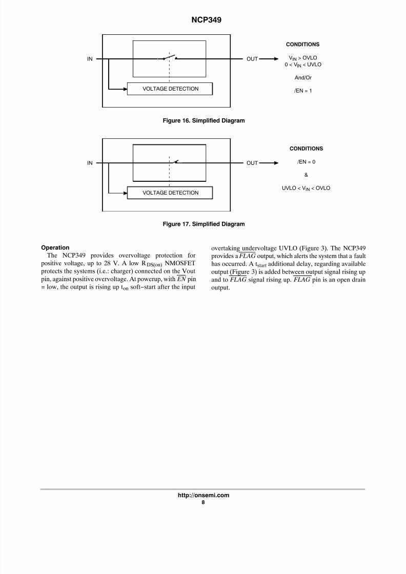
VOLTAGE DETECTION
IN OUT
CONDITIONS
VIN > OVLO
0 < VIN < UVLO
And/Or
/EN = 1
VOLTAGE DETECTION
IN OUT
CONDITIONS
/EN = 0
&
UVLO < VIN < OVLO
Figure 16. Simplified Diagram
Figure 17. Simplified Diagram
Operation
The NCP349 provides overvoltage protection forpositive voltage, up to 28 V. A low RDS(on) NMOSFETprotects the systems (i.e.: charger) connected on the Vout
pin, against positive overvoltage. At powerup, with EN pin= low, the output is rising up ton soft−start after the input
overtaking undervoltage UVLO (Figure 3). The NCP349provides a FLAG output, which alerts the system that a faulthas occurred. A tstart additional delay, regarding available
output (Figure 3) is added between output signal rising upand to FLAG signal rising up. FLAG pin is an open drainoutput.
7/24/2019 NCP349-D
http://slidepdf.com/reader/full/ncp349-d 9/12
NCP349
http://onsemi.com
9
Timer Check
Check Vin
FLAG = Low
Timer Count
Timer Check
Vin < UVLO or
Vin > OVLO
Check EN
Check EN
Vout = Vin
FLAG = High
Check Vin
Vout = Open
FLAG = High
Check Vin
Figure 18. State Machine
OVLO > Vin > UVLO
T < ton
T = ton
Reset Timer
Vout = 0
FLAG = Low
Reset Timer
Vin < UVLO or
Vin > OVLO Vout = 0
FLAG = LowTimer Count
UVLO < Vin < OVLO
EN = 0EN = 1
Vin < UVLO or
Vin > OVLO
UVLO < Vin < OVLO
EN = 0EN = 1
T = ton
Vout = Open
Vin < UVLO or
Vin > OVLO
T < ton
UVLO < Vin < OVLO
Vout = Vin
7/24/2019 NCP349-D
http://slidepdf.com/reader/full/ncp349-d 10/12
NCP349
http://onsemi.com
10
Undervoltage Lockout (UVLO)
To ensure proper operation under any conditions, thedevice has a built−in undervoltage lockout (UVLO) circuit.
During Vin positive going slope, the output remainsdisconnected from input until Vin voltage is below UVLO,
plus hysteresis, nominal. The FLAG output is tied to low aslong as Vin does not reach UVLO threshold. This circuit has
a built−in hysteresis to provide noise immunity to transient
condition. Additional UVLO thresholds ranging fromUVLO can be manufactured. Contact yourON Semiconductor representative for availability.
Overvoltage Lockout (OVLO)
To protect connected systems on Vout pin from
overvoltage, the device has a built−in overvoltage lockout(OVLO) circuit. During overvoltage condition, the output
remains disabled as long as the input voltage exceedstypical OVLO. Additional OVLO thresholds ranging from
OVLO can be manufactured. Contact your ONSemiconductor representative for availability. FLAG output is tied to low until Vin is higher than OVLO.
This circuit has a built−
in hysteresis to provide noiseimmunity to transient conditions.
FLAG Output
The NCP349 provides a FLAG output, which alertsexternal systems that a fault has occurred.
This pin is tied to low as soon the OVLO threshold isexceeded or when the Vin level is below the UVLO
threshold. When Vin level recovers normal condition,FLAG is held high, keeping in mind that an additional t start
delay has been added between available output and FLAG= high. The pin is an open drain output, thus a pull up
resistor (typically 1 M, minimum 10 k) must be added
to Vbat. Minimum Vbat supply must be 2.5 V. The FLAGlevel will always reflects Vin status, even if the device isturned off (EN = 1).
EN Input
To enable normal operation, the EN pin shall be forced
to low or connected to ground. A high level on the pin,disconnects OUT pin from IN pin. EN does not overdrive
an OVLO or UVLO fault.
Internal NMOS FET
The NCP349 includes an internal Low RDS(on) NMOSFET to protect the systems, connected on OUT pin, frompositive overvoltage. Regarding electrical characteristics,
the RDS(on), during normal operation, will create low losseson Vout pin.
As example: Rload = 8.0 , Vin = 5.0 VTypical RDS(on) = 65 m Iout = 618 mA
Vout = 8 x 0.618 = 4.95 V
NMOS losses = RDS(on) x Iout2 = 0.065 x 0.6182 = 25 mW
ESD Tests
The NCP349 input pin fully supports the IEC61000−4−2.1.0 F (minimum) must be connected between Vin and
GND, close to the device.That means, in Air condition, Vin has a ±15 kV ESD
protected input. In Contact condition, Vin has ±8.0 kV ESDprotected input.
Please refer to Figure 19 to see the IEC 61000−4−2
electrostatic discharge waveform.
Figure 19. Electrostatic Discharge Waveform
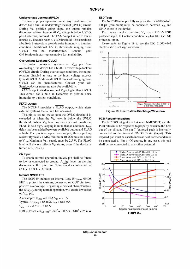
PCB Recommendations
The NCP349 integrates a 2 A rated NMOSFET, and the
PCB rules must be respected to properly evacuate the heatout of the silicon. The pin 7 (exposed pad) is internallyconnected to the internal NMOS Drain (Input). Thisexposed pad must be used to increase heat transfer and must
be connected to Pin 1. Of course, in any case, this padshall be not connected to any other potential.
Figure 20.
60
80
100
120
140
160
180
200
0 100 200 300 400 500 600 700
Copper heat spreader area (mm^2)
T h e t a J A ( C / W )
0.25
0.5
0.75
1
1.25
1.5
1.75
M
a x P o w e r ( W )
Theta JA curve with PCB cu thk 1.0 ozTheta JA curve with PCB cu thk 2.0 ozPower curve with PCB cu thk 2.0 ozPower curve with PCB cu thk 1.0 oz
7/24/2019 NCP349-D
http://slidepdf.com/reader/full/ncp349-d 11/12
NCP349
http://onsemi.com
11
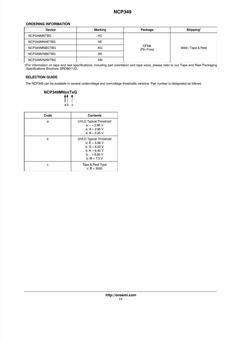
ORDERING INFORMATION
Device Marking Package Shipping†
NCP349MNTBG AC
DFN6(Pb−Free)
3000 / Tape & Reel
NCP349MNAETBG AE
NCP349MNBGTBG AG
NCP349MNBKTBG AK
NCP349MNAMTBG AM
†For information on tape and reel specifications, including part orientation and tape sizes, please refer to our Tape and Reel PackagingSpecifications Brochure, BRD8011/D.
SELECTION GUIDE
The NCP349 can be available in several undervoltage and overvoltage thresholds versions. Part number is designated as follows:
a
NCP349MNxxTxG
b c
Code Contents
a UVLO Typical Threshold
a: − = 2.95 V
a: A = 2.95 V
a: B = 3.25 V
b OVLO Typical Threshold
b: E = 5.68 V
b: G = 6.02 V
b: K = 6.40 V
b: − = 6.85 V
b: M = 7.2 V
c Tape & Reel Type
c: B = 3000
7/24/2019 NCP349-D
http://slidepdf.com/reader/full/ncp349-d 12/12
NCP349
http://onsemi.com
12
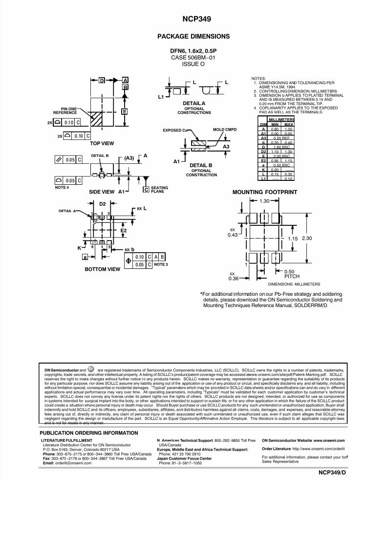
PACKAGE DIMENSIONS
DFN6, 1.6x2, 0.5PCASE 506BM−01
ISSUE O
NOTES:1. DIMENSIONING AND TOLERANCING PER
ASME Y14.5M, 1994.2. CONTROLLING DIMENSION: MILLIMETERS.
3. DIMENSION b APPLIES TO PLATED TERMINAL AND IS MEASURED BETWEEN 0.15 AND0.20 mm FROM THE TERMINAL TIP.
4. COPLANARITY APPLIES TO THE EXPOSEDPAD AS WELL AS THE TERMINALS.
É É
É É
É É
A
B
E
D
D2
E2
BOTTOM VIEW
b
e
6X
0.10 B
0.05
AC
C
K
NOTE 3
2X 0 .1 0 C
PIN ONEREFERENCE
TOP VIEW
2X 0. 10 C
NOTE 4
A
A1
(A3)
0 .0 5 C
0 .0 5 C
C
SEATING
PLANESIDE VIEW
L6X
1 3
56
DIM MIN MAX
MILLIMETERS
A 0.80 1.00A1 0.00 0.05A3 0.20 REFb 0.20 0.40D 1.60 BSCD2 1.10 1.30E 2.00 BSC
E2 0.95 1.15e 0.50 BSCK 0.20 −−−
L 0.15 0.35
*For additional information on our Pb−Free strategy and solderingdetails, please download the ON Semiconductor Soldering andMounting Techniques Reference Manual, SOLDERRM/D.
MOUNTING FOOTPRINT
Ç Ç Ç
Ç Ç Ç É É É
A1
A3
DETAIL B
MOLD CMPDEXPOSED Cu
OPTIONALCONSTRUCTION
DETAIL B
DETAIL A
1.30
1.15
0.50
0.436X
2.30
DIMENSIONS: MILLIMETERS
0.36
1
6X
L1 −−− 0.10
L1DETAIL A
L
OPTIONALCONSTRUCTIONS
L
PITCH
ON Semiconductor and are registered trademarks of Semiconductor Components Industries, LLC (SCILLC). SCILLC owns the rights to a number of patents, trademarks,copyrights, trade secrets, and other intellectual property. A listing of SCILLC’s product/patent coverage may be accessed at www.onsemi.com/site/pdf/Patent−Marking.pdf . SCILLCreserves the right to make changes without further notice to any products herein. SCILLC makes no warranty, representation or guarantee regarding the suitability of its products
for any particular purpose, nor does SCILLC assume any liability arising out of the application or use of any product or circuit, and specifically disclaims any and all liability, includingwithout limitation special, consequential or incidental damages. “Typical” parameters which may be provided in SCILLC data sheets and/or specifications can and do vary in differentapplications and actual performance may vary over time. All operating parameters, including “Typicals” must be validated for each customer application by customer’s technicalexperts. SCILLC does not convey any license under its patent rights nor the rights of others. SCILLC products are not designed, intended, or authorized for use as componentsin systems intended for surgical implant into the body, or other applications intended to support or sustain life, or for any other application in which the failure of the SCILLC productcould create a situation where personal injury or death may occur. Should Buyer purchase or use SCILLC products for any such unintended or unauthorized application, Buyer shallindemnify and hold SCILLC and its officers, employees, subsidiaries, affiliates, and distributors harmless against all claims, costs, damages, and expenses, and reasonable attorneyfees arising out of, directly or indirectly, any claim of personal injury or death associated with such unintended or unauthorized use, even if such claim alleges that SCILLC wasnegligent regarding the design or manufacture of the part. SCILLC is an Equal Opportunity/Affirmative Action Employer. This literature is subject to all applicable copyright lawsand is not for resale in any manner.
PUBLICATION ORDERING INFORMATION
N. American Technical Support: 800−282−9855 Toll FreeUSA/Canada
Europe, Middle East and Africa Technical Support:Phone: 421 33 790 2910
Japan Customer Focus CenterPhone: 81−3−5817−1050
NCP349/D
LITERATURE FULFILLMENT:Literature Distribution Center for ON SemiconductorP.O. Box 5163, Denver, Colorado 80217 USAPhone: 303−675−2175 or 800−344−3860 Toll Free USA/CanadaFax : 303−675−2176 or 800−344−3867 Toll Free USA/CanadaEmail: [email protected]
ON Semiconductor Website: www.onsemi.com
Order Literature: http://www.onsemi.com/orderlit
For additional information, please contact your locSales Representative