Embed Size (px)
Citation preview
© Semiconductor Components Industries, LLC, 2006
July, 2006 − Rev. 121 Publication Order Number:
NCP802/D
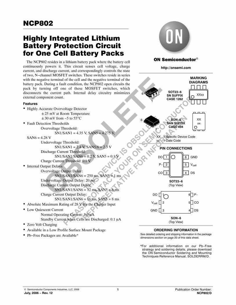
NCP802
Highly Integrated LithiumBattery Protection Circuitfor One Cell Battery Packs
The NCP802 resides in a lithium battery pack where the battery cellcontinuously powers it. This circuit senses cell voltage, chargecurrent, and discharge current, and correspondingly controls the stateof two, N−channel MOSFET switches. These switches reside in serieswith the negative terminal of the cell and the negative terminal of thebattery pack. During a fault condition, the NCP802 open circuits thepack by turning off one of these MOSFET switches, whichdisconnects the current path. Internal delay circuitry minimizesexternal component count.
Features• Highly Accurate Overvoltage Detector
�25 mV at Room Temperature�30 mV from −5 to 55°C
• Fault Detection ThresholdsOvervoltage Threshold:
SN1/SAN1 = 4.35 V, SAN5 = 4.275 V,SAN6 = 4.28 V
Undervoltage Threshold:SN1/SAN1 = 2.4 V, SAN5/6 = 2.3 V
Discharge Current Threshold:SN1/SAN1/SAN6 = 0.2 V, SAN5 = 0.1 V
Charge Current Threshold: 0.1 V• Internal Output Delays
Overvoltage Output Delay:SN1/SAN1/SAN6 = 250 ms, SAN5 = 1 ms
Undervoltage Output Delay: 20 msDischarge Current Output Delay:
SN1/SAN1/SAN6 = 12 ms, SAN5 = 6 msCharge Current Output Delay:
SN1/SAN1/SAN6 = 16 ms, SAN5 = 8 ms• Absolute Maximum Rating of 28 V for the Charger Input
• Low Quiescent CurrentNormal Operating Current: 3.0 �AStandby Current when Cells are Discharged: 0.1 �A
• Zero Volt Charging
• Available in a Low Profile Surface Mount Package
• Pb−Free Packages are Available*
SOT23−6SN SUFFIXCASE 1262
6
1
1 6
4
2
3
SOT23−6(Top View)
DO
P−
CO
GND
DS
PIN CONNECTIONS
5 Vcell
XX = Specific Device Codexx = Date Code
MARKINGDIAGRAMS
XXxx
SON−6SAN SUFFIX
CASE 494
XXxx
1
6
SON−6(Top View)
1 6
4
2
3
5
DO
GND
Vcell
P−
CO
DS
See detailed ordering and shipping information in the packagedimensions section on page 20 of this data sheet.
ORDERING INFORMATION
*For additional information on our Pb−Freestrategy and soldering details, please downloadthe ON Semiconductor Soldering and MountingTechniques Reference Manual, SOLDERRM/D.
http://onsemi.com

NCP802
http://onsemi.com2
Figure 1. Typical One Cell Lithium Ion Battery Pack
DO CO P−
Vcell
GndNCP802
Figure 2. Detailed Block Diagram
LevelShift
ShortDetector
1 3 26
5 4
Delay
VD3
VD2
VD1
Vcell DS
Gnd DO CO P−
LogicCircuit
LogicCircuit
VD4
Oscillator Counter

NCP802
http://onsemi.com3
PIN FUNCTION DESCRIPTION
Pin #SOT23−6
Pin #SON−6 Symbol Description
ÁÁÁÁÁÁÁÁÁÁ
1 ÁÁÁÁÁÁÁÁ
1 ÁÁÁÁÁÁ
DOÁÁÁÁÁÁÁÁÁÁÁÁÁÁÁÁÁÁÁÁÁÁÁÁÁÁÁÁÁÁÁÁÁÁÁÁÁÁÁÁÁÁÁÁÁÁÁÁ
This output connects to the gate of the discharge MOSFET allowing it to enable or disablebattery pack discharging.ÁÁÁÁÁ
ÁÁÁÁÁÁÁÁÁÁ
2ÁÁÁÁÁÁÁÁÁÁÁÁ
6ÁÁÁÁÁÁÁÁÁ
P−ÁÁÁÁÁÁÁÁÁÁÁÁÁÁÁÁÁÁÁÁÁÁÁÁÁÁÁÁÁÁÁÁÁÁÁÁÁÁÁÁÁÁÁÁÁÁÁÁÁÁÁÁÁÁÁÁÁÁÁÁÁÁÁÁÁÁÁÁÁÁÁÁ
This is the charger negative input pin. It connects to the excess current detectors and serves asthe common node for the CO pin during turn−off.
ÁÁÁÁÁÁÁÁÁÁÁÁÁÁÁ
3 ÁÁÁÁÁÁÁÁÁÁÁÁ
5 ÁÁÁÁÁÁÁÁÁ
COÁÁÁÁÁÁÁÁÁÁÁÁÁÁÁÁÁÁÁÁÁÁÁÁÁÁÁÁÁÁÁÁÁÁÁÁÁÁÁÁÁÁÁÁÁÁÁÁÁÁÁÁÁÁÁÁÁÁÁÁÁÁÁÁÁÁÁÁÁÁÁÁ
This output connects to the gate of the charge MOSFET switch allowing it to enable or disablebattery pack charging.
ÁÁÁÁÁÁÁÁÁÁ
4 ÁÁÁÁÁÁÁÁ
4 ÁÁÁÁÁÁ
DSÁÁÁÁÁÁÁÁÁÁÁÁÁÁÁÁÁÁÁÁÁÁÁÁÁÁÁÁÁÁÁÁÁÁÁÁÁÁÁÁÁÁÁÁÁÁÁÁ
This is the delay time reduction pin.
ÁÁÁÁÁÁÁÁÁÁÁÁÁÁÁ
5 ÁÁÁÁÁÁÁÁÁÁÁÁ
2 ÁÁÁÁÁÁÁÁÁ
VcellÁÁÁÁÁÁÁÁÁÁÁÁÁÁÁÁÁÁÁÁÁÁÁÁÁÁÁÁÁÁÁÁÁÁÁÁÁÁÁÁÁÁÁÁÁÁÁÁÁÁÁÁÁÁÁÁÁÁÁÁÁÁÁÁÁÁÁÁÁÁÁÁ
This input connects to the positive terminal of the cell for voltage monitoring and providesoperating bias for the integrated circuit.ÁÁÁÁÁ
ÁÁÁÁÁ6ÁÁÁÁÁÁÁÁ3
ÁÁÁÁÁÁGnd
ÁÁÁÁÁÁÁÁÁÁÁÁÁÁÁÁÁÁÁÁÁÁÁÁÁÁÁÁÁÁÁÁÁÁÁÁÁÁÁÁÁÁÁÁÁÁÁÁThis is the ground pin of the IC.

NCP802
http://onsemi.com4
VCELL
−P
CO
Figure 3. Overvoltage/Excess Charge Current Timing Chart
t
t
t
t
CHARGECURRENT
CHARGE/DISCHARGE
CURRENT
DISCHARGECURRENT
0
EXCESSCHARGE
CURRENTCONNECT
LOADCONNECTCHARGER
CONNECTCHARGER
CONNECTLOAD
DISCONNECTCHARGER +
CONNECT LOAD
VDD
P−
VDD
VDET1
VDET3
VDET4
Gnd
tDET1
tREL1
tDET1
tREL1
tDET4
tREL4

NCP802
http://onsemi.com5
VCELL
−P
DO
Figure 4. Undervoltage/Excess Discharge Current Timing Chart
t
t
t
t
EXCESSDISCHARGECURRENTCONNECT
CHARGERCONNECT
LOAD
CONNECTCHARGERCONNECT
LOAD OPENOPENSHORT
0
CHARGECURRENT
DISCHARGECURRENT
CHARGE/DISCHARGE
CURRENT
VDD
Gnd
Gnd
VDDVshort
VDET3
VDET4
VDET2
tREL3tREL2 tREL2 tREL3
tshorttDET3tDET2tDET2

NCP802
http://onsemi.com6
MAXIMUM RATINGS
Rating Symbol Value Unit
ÁÁÁÁÁÁÁÁÁÁÁÁÁÁÁÁÁÁÁÁÁÁÁÁÁÁÁÁÁÁÁÁÁÁ
Supply Voltage (Pin 5 to Pin 6) ÁÁÁÁÁÁÁÁÁÁÁÁ
VDDÁÁÁÁÁÁÁÁÁÁÁÁÁÁÁÁÁÁ
−0.3 to 12 ÁÁÁÁÁÁÁÁ
V
ÁÁÁÁÁÁÁÁÁÁÁÁÁÁÁÁÁÁÁÁÁÁÁÁÁÁÁÁÁÁÁÁÁÁ
Input Voltage ÁÁÁÁÁÁÁÁÁÁÁÁ
ÁÁÁÁÁÁÁÁÁÁÁÁÁÁÁÁÁÁ
ÁÁÁÁÁÁÁÁP− Pin Voltage (Pin 5 to Pin 2) VP− VDD + 0.3 to VDD − 28 V
DS Pin Voltage (Pin 4 to Pin 6) VDS −0.3 to 12 VÁÁÁÁÁÁÁÁÁÁÁÁÁÁÁÁÁÁÁÁÁÁÁÁÁÁÁÁÁÁÁÁÁÁ
Output VoltageÁÁÁÁÁÁÁÁÁÁÁÁ
ÁÁÁÁÁÁÁÁÁÁÁÁÁÁÁÁÁÁ
ÁÁÁÁÁÁÁÁCO Pin Voltage (Pin 3 to Pin 2) VCO VDD + 0.3 to VDD − 28 V
DO Pin Voltage (Pin 1 to Pin 6) VDO −0.3 to 12 VÁÁÁÁÁÁÁÁÁÁÁÁÁÁÁÁÁÁÁÁÁÁÁÁÁÁÁÁÁÁÁÁÁÁPower Dissipation
ÁÁÁÁÁÁÁÁÁÁÁÁPD
ÁÁÁÁÁÁÁÁÁÁÁÁÁÁÁÁÁÁ150
ÁÁÁÁÁÁÁÁmWÁÁÁÁÁÁÁÁÁÁÁÁÁÁÁÁÁ
ÁÁÁÁÁÁÁÁÁÁÁÁÁÁÁÁÁOperating Ambient Temperature RangeÁÁÁÁÁÁÁÁÁÁÁÁTA
ÁÁÁÁÁÁÁÁÁÁÁÁÁÁÁÁÁÁ−40 to 85
ÁÁÁÁÁÁÁÁ°CÁÁÁÁÁÁÁÁÁÁÁÁÁÁÁÁÁ
ÁÁÁÁÁÁÁÁÁÁÁÁÁÁÁÁÁÁÁÁÁÁÁÁÁÁÁÁÁÁÁÁÁÁ
Storage TemperatureÁÁÁÁÁÁÁÁÁÁÁÁÁÁÁÁÁÁ
Tstg
ÁÁÁÁÁÁÁÁÁÁÁÁÁÁÁÁÁÁÁÁÁÁÁÁÁÁÁ
−55 to 125ÁÁÁÁÁÁÁÁÁÁÁÁ
°C
Stresses exceeding Maximum Ratings may damage the device. Maximum Ratings are stress ratings only. Functional operation above theRecommended Operating Conditions is not implied. Extended exposure to stresses above the Recommended Operating Conditions may affectdevice reliability.
ATTRIBUTES
Characteristics Value
ESD ProtectionHuman Body Model (HBM) (C = 100 pF, R = 1.5 k�)Machine Model (MM) (C = 200 pF, R = 0 �)
≤1 kV≤150 V
Moisture Sensitivity, Indefinite Time Out of Drypack (Note 1) Level 1
Latch−up Current Maximum Rating per JEDEC standard JESD78 ≤150 mA
1. For additional Moisture Sensitivity information, refer to Application Note AND8003/D.

NCP802
http://onsemi.com7
ELECTRICAL CHARACTERISTICS(TA = 25°C, for min/max values TA is the operating junction temperature that applies, unless otherwise noted.)
Characteristic Symbol Min Typ Max Unit Note 2
VOLTAGE SENSING
ÁÁÁÁÁÁÁÁÁÁÁÁÁÁÁÁÁÁCell Charging Cutoff (Pin 5 to Pin 6) ÁÁÁVDET1ÁÁÁÁÁÁÁÁÁÁÁÁÁÁÁÁÁÁOvervoltage Threshold, VDD Increasing(R1 = 330 �)
TA = 25°C SN1/SAN1T1 4.325 4.35 4.375 VTA = −5°C to 55°C SN1/SAN1T1 4.32 4.35 4.38 V ATA = 25°C SAN5T1 4.25 4.275 4.30 VTA = −5°C to 55°C SAN5T1 4.245 4.275 4.305 V ATA = 25°C SAN6T1 4.255 4.28 4.305 VTA = −5°C to 55°C SAN6T1 4.25 4.28 4.31 V A
Overvoltage Delay Time(VDD = 3.6 V to 4.4 V) SN1/SAN1T1/SAN6T1
SAN5T1
tDET10.1750.7
0.25001.0
0.3251.3
s A
Overvoltage Release Time(VDD = 4.0 V, VP− = 0 V to 1.0 V)
tREL1 11 16 21 ms B
Cell Discharging Cutoff (Pin 5 to Pin 6)Undervoltage Threshold, VDD Decreasing SN1/SAN1T1
SAN5T1/SAN6T1
VDET22.342.24
2.42.3
2.462.36
V C
Undervoltage Time(VDD = 3.6 V to 2.2 V)
tDET2 14 20 26 ms C
Undervoltage Release Delay Time(VDD = 3.0 V, VP− = 3.0 V to 0 V)
tREL2 0.7 1.2 1.7 ms D
ÁÁÁÁÁÁÁÁÁÁÁÁÁÁÁÁÁÁÁÁÁÁÁÁÁÁÁÁÁÁÁÁÁÁÁÁÁÁÁÁÁÁÁÁÁÁÁÁÁÁÁÁÁÁÁÁÁÁÁÁÁÁÁÁÁÁ
CURRENT SENSING
ÁÁÁÁÁÁÁÁÁÁÁÁÁÁÁÁÁÁÁÁÁÁÁÁÁÁÁÁÁÁÁÁÁÁÁÁÁÁÁÁÁÁÁÁÁÁÁÁÁÁÁÁÁÁ
Excess Discharge Current Threshold, VP− IncreasingSN1T1/SAN1T1/SAN6T1
SAN5T1
ÁÁÁÁÁÁÁÁÁ
VDET3ÁÁÁÁÁÁÁÁÁÁÁÁ
0.1800.080
ÁÁÁÁÁÁÁÁÁÁÁÁ
0.2000.100
ÁÁÁÁÁÁÁÁÁÁÁÁ
0.2200.120
ÁÁÁÁÁÁÁÁÁ
VÁÁÁÁÁÁÁÁÁ
K
ÁÁÁÁÁÁÁÁÁÁÁÁÁÁÁÁÁÁÁÁÁÁÁÁÁÁÁÁÁÁÁÁÁÁÁÁÁÁÁÁÁÁÁÁÁÁÁÁÁÁÁÁÁÁ
Excess Discharge Current Delay Time(VDD = 3.0 V, VP− = 0 V to 1.0 V) SN1T1/SAN1T1/SAN6T1
SAN5T1
ÁÁÁÁÁÁÁÁÁ
tDET3ÁÁÁÁÁÁÁÁÁÁÁÁ
8.04.0
ÁÁÁÁÁÁÁÁÁÁÁÁ
126.0
ÁÁÁÁÁÁÁÁÁÁÁÁ
168.0
ÁÁÁÁÁÁÁÁÁ
msÁÁÁÁÁÁÁÁÁ
K
ÁÁÁÁÁÁÁÁÁÁÁÁÁÁÁÁÁÁÁÁÁÁÁÁÁÁÁÁÁÁÁÁÁÁÁÁÁÁÁÁÁÁÁÁÁÁÁÁÁÁÁÁÁÁ
Excess Discharge Current Release Time(VDD = 3.0 V, VP− = 3.0 V to 0 V)
ÁÁÁÁÁÁÁÁÁ
tREL3ÁÁÁÁÁÁÁÁÁÁÁÁ
0.7ÁÁÁÁÁÁÁÁÁÁÁÁ
1.2ÁÁÁÁÁÁÁÁÁÁÁÁ
1.7ÁÁÁÁÁÁÁÁÁ
msÁÁÁÁÁÁÁÁÁ
K
ÁÁÁÁÁÁÁÁÁÁÁÁÁÁÁÁÁÁÁÁÁÁÁÁÁÁÁÁÁÁÁÁÁÁÁÁ
Excess Charge Current Threshold, VP− Decreasing ÁÁÁÁÁÁ
VDET4ÁÁÁÁÁÁÁÁ
−0.13ÁÁÁÁÁÁÁÁ
−0.1ÁÁÁÁÁÁÁÁ
−0.07ÁÁÁÁÁÁ
VÁÁÁÁÁÁ
E
ÁÁÁÁÁÁÁÁÁÁÁÁÁÁÁÁÁÁÁÁÁÁÁÁÁÁÁÁÁÁÁÁÁÁÁÁÁÁÁÁÁÁÁÁÁÁÁÁÁÁÁÁÁÁ
Excess Charge Current Delay Time(VDD = 3.0 V, VP− = 0 V to −1.0 V) SN1T1/SAN1T1/SAN6T1
SAN5T1
ÁÁÁÁÁÁÁÁÁ
tDET4ÁÁÁÁÁÁÁÁÁÁÁÁ
115.0
ÁÁÁÁÁÁÁÁÁÁÁÁ
168.0
ÁÁÁÁÁÁÁÁÁÁÁÁ
2111
ÁÁÁÁÁÁÁÁÁ
msÁÁÁÁÁÁÁÁÁ
E
ÁÁÁÁÁÁÁÁÁÁÁÁÁÁÁÁÁÁÁÁÁÁÁÁÁÁÁÁÁÁÁÁÁÁÁÁÁÁÁÁÁÁÁÁÁÁÁÁÁÁÁÁÁÁ
Excess Charge Current Release Time(VDD = 3.0 V, VP− = −1.0 V to 0 V)
ÁÁÁÁÁÁÁÁÁ
tREL4ÁÁÁÁÁÁÁÁÁÁÁÁ
0.7ÁÁÁÁÁÁÁÁÁÁÁÁ
1.2ÁÁÁÁÁÁÁÁÁÁÁÁ
1.7ÁÁÁÁÁÁÁÁÁ
msÁÁÁÁÁÁÁÁÁ
E
ÁÁÁÁÁÁÁÁÁÁÁÁÁÁÁÁÁÁÁÁÁÁÁÁÁÁÁÁÁÁÁÁÁÁÁÁÁÁÁÁÁÁÁÁÁÁÁÁÁÁÁÁÁÁ
Short Protection Voltage(VDD = 3.0 V)
ÁÁÁÁÁÁÁÁÁ
VSHORTÁÁÁÁÁÁÁÁÁÁÁÁ
VDD −1.4ÁÁÁÁÁÁÁÁÁÁÁÁ
VDD −1.1ÁÁÁÁÁÁÁÁÁÁÁÁ
VDD −0.8ÁÁÁÁÁÁÁÁÁ
VÁÁÁÁÁÁÁÁÁ
K
ÁÁÁÁÁÁÁÁÁÁÁÁÁÁÁÁÁÁÁÁÁÁÁÁÁÁÁÁÁÁÁÁÁÁÁÁ
Short Protection Delay Time(VDD = 3.0 V, VP− = 0 V to 3.0 V)
ÁÁÁÁÁÁ
tSHORTÁÁÁÁÁÁÁÁ
250 ÁÁÁÁÁÁÁÁ
400ÁÁÁÁÁÁÁÁ
600ÁÁÁÁÁÁ
�sÁÁÁÁÁÁ
K
ÁÁÁÁÁÁÁÁÁÁÁÁÁÁÁÁÁÁÁÁÁÁÁÁÁÁÁÁÁÁÁÁÁÁÁÁÁÁÁÁÁÁÁÁÁÁÁÁÁÁÁÁÁÁ
Reset Resistance(VDD = 3.6 V, VP− = 1.0 V)
ÁÁÁÁÁÁÁÁÁ
RSHORTÁÁÁÁÁÁÁÁÁÁÁÁ
15ÁÁÁÁÁÁÁÁÁÁÁÁ
30ÁÁÁÁÁÁÁÁÁÁÁÁ
45ÁÁÁÁÁÁÁÁÁ
k�ÁÁÁÁÁÁÁÁÁ
K
2. Indicates test circuits shown on pages 16 and 17.

NCP802
http://onsemi.com8
ELECTRICAL CHARACTERISTICS(TA = 25°C, for min/max values TA is the operating junction temperature that applies, unless otherwise noted.)
Characteristic Symbol Min Typ Max Unit Note 3
ÁÁÁÁÁÁÁÁÁÁÁÁÁÁÁÁÁÁÁÁÁÁÁÁÁÁÁÁÁÁÁÁÁÁÁÁÁÁÁÁÁÁÁÁÁÁÁÁÁÁÁÁÁÁÁÁÁÁÁÁÁÁÁÁÁÁ
OUTPUTS
ÁÁÁÁÁÁÁÁÁÁÁÁÁÁÁÁÁÁÁÁÁÁÁÁÁÁÁÁÁÁÁÁÁÁÁÁÁÁÁÁ
Charge Gate Drive Output Low (Pin 3 to Pin 2) (VDD = 4.5 V, Io = 50 �A) ÁÁÁÁÁÁ
Vol1ÁÁÁÁÁÁÁÁ
− ÁÁÁÁÁÁ
0.4ÁÁÁÁÁÁ
0.5ÁÁÁÁÁÁ
VÁÁÁÁÁÁ
G
ÁÁÁÁÁÁÁÁÁÁÁÁÁÁÁÁÁÁÁÁÁÁÁÁÁÁÁÁÁÁÁÁÁÁÁÁÁÁÁÁ
Charge Gate Drive Output High (Pin 5 to Pin 3) (VDD = 3.9 V, Io = −50 �A) ÁÁÁÁÁÁ
Voh1ÁÁÁÁÁÁÁÁ
3.4 ÁÁÁÁÁÁ
3.7ÁÁÁÁÁÁ
−ÁÁÁÁÁÁ
VÁÁÁÁÁÁ
H
ÁÁÁÁÁÁÁÁÁÁÁÁÁÁÁÁÁÁÁÁÁÁÁÁÁÁÁÁÁÁÁÁÁÁÁÁÁÁÁÁ
Discharge Gate Drive Output Low (Pin 1 to Pin 6)(VDD = 2.0 V, Io = 50 �A)
ÁÁÁÁÁÁ
Vol2ÁÁÁÁÁÁÁÁ
− ÁÁÁÁÁÁ
0.2ÁÁÁÁÁÁ
0.5ÁÁÁÁÁÁ
VÁÁÁÁÁÁ
I
ÁÁÁÁÁÁÁÁÁÁÁÁÁÁÁÁÁÁÁÁÁÁÁÁÁÁÁÁÁÁÁÁÁÁÁÁÁÁÁÁÁÁÁÁÁÁÁÁÁÁÁÁÁÁÁÁÁÁÁÁ
Discharge Gate Drive Output High (Pin 5 to Pin 1)(VDD = 3.9 V, Io = −50 �A)
ÁÁÁÁÁÁÁÁÁ
Voh2ÁÁÁÁÁÁÁÁÁÁÁÁ
3.4ÁÁÁÁÁÁÁÁÁ
3.7ÁÁÁÁÁÁÁÁÁ
−ÁÁÁÁÁÁÁÁÁ
VÁÁÁÁÁÁÁÁÁ
J
ÁÁÁÁÁÁÁÁÁÁÁÁÁÁÁÁÁÁÁÁÁÁÁÁÁÁÁÁÁÁÁÁÁÁÁÁÁÁÁÁÁÁÁÁÁÁÁÁÁÁÁÁÁÁÁÁÁÁÁÁÁÁÁÁÁÁ
DELAY SHORTENING (DS PIN)
ÁÁÁÁÁÁÁÁÁÁÁÁÁÁÁÁÁÁÁÁÁÁÁÁÁÁÁÁÁÁÁÁÁÁÁÁÁÁÁÁÁÁÁÁÁÁÁÁÁÁÁÁÁÁÁÁÁÁÁÁ
DS Pin High Input Voltage ÁÁÁÁÁÁÁÁÁ
VIHÁÁÁÁÁÁÁÁÁÁÁÁ
VDD−0.5ÁÁÁÁÁÁÁÁÁ
− ÁÁÁÁÁÁÁÁÁ
VDD+0.3ÁÁÁÁÁÁÁÁÁ
VÁÁÁÁÁÁÁÁÁ
F
ÁÁÁÁÁÁÁÁÁÁÁÁÁÁÁÁÁÁÁÁÁÁÁÁÁÁÁÁÁÁÁÁÁÁÁÁÁÁÁÁ
DS Pin Middle Input Voltage (VDD = 3.6 to 4.4 V) ÁÁÁÁÁÁ
VIMÁÁÁÁÁÁÁÁ
1.05 ÁÁÁÁÁÁ
− ÁÁÁÁÁÁ
VDD−1.1ÁÁÁÁÁÁ
VÁÁÁÁÁÁ
F
ÁÁÁÁÁÁÁÁÁÁÁÁÁÁÁÁÁÁÁÁÁÁÁÁÁÁÁÁÁÁÁÁÁÁÁÁÁÁÁÁ
DS Pin Pull−down Resistance (VDD = 3.6 V)ÁÁÁÁÁÁ
RDSÁÁÁÁÁÁÁÁ
0.5ÁÁÁÁÁÁ
1.3ÁÁÁÁÁÁ
2.5ÁÁÁÁÁÁ
M�ÁÁÁÁÁÁ
FÁÁÁÁÁÁÁÁÁÁÁÁÁÁÁÁÁÁÁÁÁÁÁÁÁÁÁÁÁÁÁÁÁÁÁÁÁÁÁÁÁÁÁÁÁÁÁÁÁÁÁÁÁÁÁÁÁÁÁÁÁÁÁÁÁÁ
TOTAL DEVICEÁÁÁÁÁÁÁÁÁÁÁÁÁÁÁÁÁÁÁÁÁÁÁÁÁÁÁÁÁÁÁÁÁÁÁÁÁÁÁÁ
Supply CurrentÁÁÁÁÁÁ
IcellÁÁÁÁÁÁÁÁ
ÁÁÁÁÁÁ
ÁÁÁÁÁÁ
ÁÁÁÁÁÁ
ÁÁÁÁÁÁ
LOperating (VDD = 3.9 V, VP− = 0 V) − 3.0 6.0 �AStandby (VDD = 2.0 V) − − 0.1 �AÁÁÁÁÁÁÁÁÁÁÁÁÁÁÁÁÁÁÁÁ
ÁÁÁÁÁÁÁÁÁÁÁÁÁÁÁÁÁÁÁÁOperating VoltageÁÁÁÁÁÁVDD
ÁÁÁÁÁÁÁÁ1.5
ÁÁÁÁÁÁ−
ÁÁÁÁÁÁ5.0
ÁÁÁÁÁÁV
ÁÁÁÁÁÁ−ÁÁÁÁÁÁÁÁÁÁÁÁÁÁÁÁÁÁÁÁ
ÁÁÁÁÁÁÁÁÁÁÁÁÁÁÁÁÁÁÁÁÁÁÁÁÁÁÁÁÁÁÁÁÁÁÁÁÁÁÁÁ
Minimum Operating Cell Voltage for Zero Volt Charging(Pin 5 to Pin 2) (VDD − Gnd = 0 V)
ÁÁÁÁÁÁÁÁÁ
VST
ÁÁÁÁÁÁÁÁÁÁÁÁ
−ÁÁÁÁÁÁÁÁÁ
−ÁÁÁÁÁÁÁÁÁ
1.5ÁÁÁÁÁÁÁÁÁ
VÁÁÁÁÁÁÁÁÁ
M
3. Indicates test circuits shown on pages 16 and 17.

NCP802
http://onsemi.com9
1
0
1.2
1.4
0.8
0.6
0.4
0.2
1.6
1.8
0.40
0.25
0.00
0.30
0.35
0.45
0.20
0.15
0.10
0.05
−50
4.35
0
OV
ER
VO
LTA
GE
TH
RE
SH
OLD
, VD
ET
1 (V
)
4.30
TA, AMBIENT TEMPERATURE (°C)
Figure 5. Overvoltage Threshold vs.Temperature
Figure 6. Overvoltage Delay Time vs.Temperature
Figure 7. Overvoltage Release Time vs.Temperature
TA, AMBIENT TEMPERATURE (°C)
Figure 8. Undervoltage Threshold vs.Temperature
OV
ER
VO
LTA
GE
RE
LEA
SE
TIM
E, t
RE
L1 (
ms)
TA, AMBIENT TEMPERATURE (°C)
4.36
4.37
50 100
4.34
4.33
4.32
4.31
−50 500 100
OV
ER
VO
LTA
GE
DE
LAY
TIM
E, t
DE
T1
(s)
−60
20
40
5
0−20
30
10
15
25
0−40 20 60 80 U
ND
ER
VO
LTA
GE
TH
RE
SH
OLD
, VD
ET
2 (V
)
100 −50 0
TA, AMBIENT TEMPERATURE (°C)
50 100
2.41
2.36
2.42
2.43
2.40
2.39
2.38
2.37
−50 0
Figure 9. Undervoltage Delay Time vs.Temperature
TA, AMBIENT TEMPERATURE (°C)
50 100
25
UN
DE
RV
OLT
AG
E D
ELA
Y T
IME
t DE
T2
(ms)
0
30
35
20
15
10
5
−60 0
Figure 10. Undervoltage Release Time vs.Temperature
TA, AMBIENT TEMPERATURE (°C)
60 100UN
DE
RV
OLT
AG
E R
ELE
AS
E T
IME
, tR
EL2
(m
s)
−40 −20 20 40 80

NCP802
http://onsemi.com10
10
0
15
20
5
25
30
16
10
0
12
14
18
8
6
4
2
0.200
EX
CE
SS
DIS
CH
AR
GE
CU
RR
EN
T T
HR
ES
HO
LD, V
DE
T3
(V)
0.190
TA, AMBIENT TEMPERATURE (°C)
Figure 11. Excess Discharge CurrentThreshold vs. Temperature
Figure 12. Excess Discharge Current DelayTime vs. Temperature
Figure 13. Excess Discharge Current ReleaseTime vs. Temperature
TA, AMBIENT TEMPERATURE (°C)
Figure 14. Reset Resistance vs. Temperature
EX
CE
SS
DIS
CH
AR
GE
CU
RR
EN
T R
ELE
AS
ED
ELA
Y T
IME
, tR
EL2
(m
s)
TA, AMBIENT TEMPERATURE (°C)
0.205
0.210
0.195
EX
CE
SS
DIS
CH
AR
GE
CU
RR
EN
TD
ELA
Y T
IME
, tD
ET
3 (m
s)
−60 400−20−40 20 60 80
RE
SE
T R
ES
ISTA
NC
E, R
SH
OR
T (k
�)
100
TA, AMBIENT TEMPERATURE (°C)
30
0
40
50
20
10
−50 0
Figure 15. Excess Charge Current Thresholdvs. Temperature
TA, AMBIENT TEMPERATURE (°C)
50 100
−0.105
EX
CE
SS
CH
AR
GE
CU
RR
EN
T T
HR
ES
HO
LD V
DE
T4
(V)
−0.090
−0.110
−0.100
−0.095
−60 0
Figure 16. Excess Charge Current Delay Timevs. Temperature
TA, AMBIENT TEMPERATURE (°C)
60 100
EX
CE
SS
CH
AR
GE
CU
RR
EN
T D
ELA
Y T
IME
, tR
EL4
(m
s)
−40 −20 20 40 80
−60 0 60 100−40 −20 20 40 80
1.6
1
0
1.2
1.4
1.8
0.8
0.6
0.4
0.2
−60 0 60 100−40 −20 20 40 80−60 400−20−40 20 60 80 100
VDD = 3.6 V

NCP802
http://onsemi.com11
1.5
0
2
0.5
2.5
2.15
2.00
1.80
2.05
2.10
2.20
1.95
1.90
1.85
1.4
EX
CE
SS
CH
AR
GE
CU
RR
EN
T R
ELE
AS
ET
IME
, tR
EL4
(m
s)
0
TA, AMBIENT TEMPERATURE (°C)
Figure 17. Excess Charge Current ReleaseTime vs. Temperature
Figure 18. Short Protection Threshold vs.Temperature
Figure 19. Short Protection Delay Time vs.Temperature
TA, AMBIENT TEMPERATURE (°C)
Figure 20. DS Pin High Input Minimum Voltagevs. Temperature
SH
OR
T P
RO
TE
CT
ION
DE
LAY
TIM
E, t
SH
OR
T (�s)
TA, AMBIENT TEMPERATURE (°C)
1.6
1.8
1.2
1
0.8
0.6
−50 500 100SH
OR
T P
RO
TE
CT
ION
VO
LTA
GE
, VS
HO
RT (
V)
500
200
700
300
400
600
0 DS
PIN
HIG
H M
INIM
UM
VO
LTA
GE
, VIH
(V
)
TA, AMBIENT TEMPERATURE (°C)
−50 0
Figure 21. DS Pin Middle Input MinimumVoltage vs. Temperature
TA, AMBIENT TEMPERATURE (°C)
50 100
2.5
DS
PIN
MID
DLE
INP
UT
MIN
IMU
M V
OLT
AG
E, V
IM (
V)
0
3
2
1.5
1
0.5
Figure 22. DS Pin Pull−Down Resistance vs.Temperature
TA, AMBIENT TEMPERATURE (°C)
DS
PIN
PU
LL−
DO
WN
RE
SIS
TAN
CE
−50 0 50 100
1
1.5
0
2
0.5
2.5
1
3
−50 0 50 100−50 0 50 100
−60 400−20−40 20 60 80 100
0.4
0.2
100
VDD = 3.0 V
VDD = 3.0 V
VDD = 3.6 V
VDD = 3.6 V to 4.4 V

NCP802
http://onsemi.com12
0
0.06
0.08
0.04
0.02
0.1
0.3
CO
NC
H D
RIV
ER
OU
TP
UT,
Vol
1 (V
)
0
TA, AMBIENT TEMPERATURE (°C)
Figure 23. CO NCH Driver Output vs.Temperature
Figure 24. CO PCH Driver Output vs.Temperature
Figure 25. DO NCH Driver Output vs.Temperature
TA, AMBIENT TEMPERATURE (°C)
Figure 26. DO PCH Driver Output vs.Temperature
DO
NC
H D
RIV
ER
OU
TP
UT,
Vol
2 (V
)
TA, AMBIENT TEMPERATURE (°C)
0.4
0.5
0.2
0.1
−50 500 100
CO
PC
H D
RIV
ER
OU
TP
UT,
Voh
1 (V
)
−60
0.2
400−20
0.4
0.1
0.3
0−40 20 60 80
DO
PC
H D
RIV
ER
OU
TP
UT,
Voh
2 (V
)
100 −50 0
TA, AMBIENT TEMPERATURE (°C)
50 1003.5
3.9
3.8
3.6
−50 0
Figure 27. Operating Current vs. Temperature
TA, AMBIENT TEMPERATURE (°C)
50 100
4
OP
ER
AT
ING
CU
RR
EN
T I c
ell (�A
)
0
5
6
3
2
1
Figure 28. Standby Current vs. Temperature
TA, AMBIENT TEMPERATURE (°C)
STA
ND
BY
CU
RR
EN
T I c
ell (�A
)
3.7
−60 400−20−40 20 60 80 1003.5
3.9
3.8
3.6
3.7
−50 0 50 100

NCP802
http://onsemi.com13
16
10
0
12
14
18
8
6
4
2
4.0
0.20
4.5
OV
ER
VO
LTA
GE
DE
LAY
TIM
E, t
DE
T1
(s)
0.00
VDD, OPERATING VOLTAGE (V)
Figure 29. Overvoltage Delay Time vs.Operating Voltage
Figure 30. Overvoltage Release Time vs.Operating Voltage
Figure 31. Undervoltage Delay Time vs.Operating Voltage
VDD, OPERATING VOLTAGE (V)
Figure 32. Undervoltage Release Time vs.Operating Voltage
VDD, OPERATING VOLTAGE (V)
0.25
0.30
5.0 6.0
0.15
0.10
0.05
3.0 4.03.5 4.5OV
ER
VO
LTA
GE
RE
LEA
SE
TIM
E, t
RE
L1 (
s)
1.0
16
4
1.5
22
8
12
20
02.0 U
ND
ER
VO
LTA
GE
RE
LEA
SE
TIM
E, t
RE
L2 (
ms)
2.5
VDD, OPERATING VOLTAGE (V)
Figure 33. Excess Discharge Current DelayTime vs. Operating Voltage
VDD, OPERATING VOLTAGE (V)
10
0
12
14
8
6
4
2
Figure 34. Excess Discharge Current ReleaseTime vs. Operating Voltage
VDD, OPERATING VOLTAGE (V)
EX
CE
SS
DIS
CH
AR
GE
CU
RR
EN
T R
ELE
AS
ED
ELA
Y T
IME
t RE
L2 (
ms)
1
0
1.2
1.4
0.8
0.6
0.4
0.2
2.0 3.52.5 4.53.0 4.02.0 3.52.5 4.53.0 4.0
EX
CE
SS
DIS
CH
AR
GE
CU
RR
EN
T D
ELA
YT
IME
t DE
T3
(ms)
2.0 3.52.5 4.53.0 4.0
1
0
1.2
1.4
0.8
0.6
0.4
0.2
UN
DE
RV
OLT
AG
E D
ELA
Y T
IME
, tD
ET
2 (m
s)
14
2
6
10
18
5.5

NCP802
http://onsemi.com14
1.5
0
2
1
0.5
2.5
1
0
1.2
1.4
0.8
0.6
0.4
0.2
14
0
VDD, OPERATING VOLTAGE (V)
Figure 35. Excess Charge Current Delay Timevs. Operating Voltage
Figure 36. Excess Charge Current ReleaseTime vs. Operating Voltage
Figure 37. Short Protection Delay Time vs.Operating Voltage
VDD, OPERATING VOLTAGE (V)
Figure 38. Undervoltage Thresholds vs. R1
SH
OR
T P
RO
TE
CT
ION
DE
LAY
TIM
E, t
SH
OR
T (�s)
VDD, OPERATING VOLTAGE (V)
16
18
12
10
8
6
2.0 3.52.5 4.5
EX
CE
SS
CH
AR
GE
CU
RR
EN
T R
ELE
AS
ET
IME
, tR
EL4
(m
s)
2
500
200
3.53
700
300
400
600
02.5 4
UN
DE
RV
OLT
AG
E T
HR
ES
HO
LD (
V)
4.5
R1 (�)
2.425
2.416
2.426
2.427
2.424
2.423
2.422
2.421
0 300
Figure 39. Overvoltage Thresholds vs. R1
R1 (�)
500 1000
4.292
OV
ER
VO
LTA
GE
TH
RE
SH
OLD
(V
)
4.288
4.293
4.294
4.291
4.29
4.289
0 150
Figure 40. Charger Voltage to Release fromUndervoltage vs. R2
R2 (k�)
300
CH
AR
GE
R V
OLT
AG
E T
O R
ELE
AS
EF
RO
M U
ND
ER
VO
LTA
GE
(V
)
50 100 200 250100 200 400 600 700 800 900
2.419
2.420
2.418
2.417
0 300 500 1000100 200 400 600 700 800 900
100
3.0 4.02.0 3.52.5 4.53.0 4.0
4
2
EX
CE
SS
CH
AR
GE
CU
RR
EN
T D
ELA
YT
IME
, tR
EL4
(m
s)
UndervoltageReleaseThreshold
UndervoltageThreshold
OvervoltageReleaseThreshold
OvervoltageThreshold
VDD = 4.25 V

NCP802
http://onsemi.com15
−50
1.6
0
MIN
IMU
M O
PE
RA
TIN
G V
OLT
AG
E F
OR
0 V
CH
AR
GIN
G V
ST (
V)
0
Figure 41. Minimum Operating Voltage for 0 VCharging vs. Temperature
TA, AMBIENT TEMPERATURE (°C)
1.8
2
50 100
1.4
1.2
0.2
1
0.8
0.6
0.4
VDD − GND = 0

NCP802
http://onsemi.com16
VCELL
P−
GND
CO
A
B
C
E
F
G
H
Figure 42. Test Circuits
V
CO
VCELL
P−
GND
DOV
VCELL
P−
GND
DO
D
V
V
A
VCELL
P−
GNDV
CO A
V
A
VCELL
P−
GND
VCELL
P−
GND
CO
DO
VCELL
P−
GND
DS
VCELL
P−
GND
CO

NCP802
http://onsemi.com17
DO
V
VCELL
P−
GNDV
DO A
I
J
M
K
L
Figure 43. Test Circuits
V
V
VCO
A
A
A
VCELL
P−
GND
DO
VCELL
P−
GND
DO
VCELL
P−
GND
VCELL
P−
GND
Overvoltage DetectionThe overvoltage detector (VD1) monitors the VCELL pin
voltage. When the VCELL voltage crosses the overvoltagedetector threshold (VDET1) from a low value to a valuehigher than VDET1, VD1 detects an over−chargingcondition. The NCP802 then turns off an external, chargecontrol, N−channel, MOSFET by driving the CO pin to itslow level. A level shifter, incorporated in a buffer driver forthe CO pin, drives the low level of the CO pin to the P− pinvoltage, which is connected to the source of the chargecontrol MOSFET by a resistor. The high level of the CO pinis driven to the VCELL voltage with a CMOS buffer.
To reset the CO pin to its high level, the voltage at theVCELL pin must decrease to a level lower than VDET1. Theovervoltage detector does not reset after the battery voltagefalls below some hysteresis voltage. The NCP802 will not
reset from an overvoltage fault as long as a charger isconnected to the battery. Rather, the excess−dischargecurrent detector (VD3) signals the IC to reset from anovervoltage condition by detecting a load while in anovervoltage condition. When the P− pin voltage becomesequal to or greater than than the excess discharge−currentdetector threshold (VDET3) during an overvoltage fault, theNCP802 senses the voltage drop across the chargeMOSFET’s body diode induced by the load current. It thenresets from the overvoltage state.
There are internal, fixed delay times for both the detectionand release from an overvoltage condition. If the fault orreset conditions are shorter than their respective delay times,the NCP802 ignores that condition and stays in its previousstate.

NCP802
http://onsemi.com18
Undervoltage DetectionThe undervoltage detector (VD2) monitors the VCELL
pin voltage. When the VCELL voltage crosses theundervoltage threshold (VDET2) from a high value to avalue lower than VDET2, VD2 senses an undervoltagecondition, and an external, discharge control, N−channelMOSFET turns off by driving the DO pin to its low level.The low level of DO is set to GND and the high level toVCELL.
To reset the DO pin to its high level, one must connect acharger to the battery pack. While the VCELL voltageremains under VDET2, charge−current can flow through theparasitic diode of the external discharge control MOSFET.Once the VCELL voltage rises above VDET2, the NCP802drives DO high. Connecting a charger to the battery packdrives the DO level high instantaneously when the VCELLvoltage is higher than VDET2. VD2 has no hysteresis.
After VD2 detects an undervoltage condition, theNCP802 enters a low supply current, standby mode.Maximum standby current equals 0.1 �A at VCELL equalto 2.0 V. An internal pull−up disables all the device functionsand thus drastically lowers quiescent current. When thecharger connects to the battery, it pulls small levels ofcurrent from the P− pin. This overcomes the internal pull−upand allows the NCP802 to reset.
There are internal, fixed delay times for both the detectionand release from an undervoltage condition. If the fault orreset conditions are shorter than their respective delay times,the NCP802 ignores that condition and stays in its previousstate.
Excess Discharge−Current/Short Circuit DetectionThe excess discharge−current detector (VD3) and the
short circuit detector can function when the controlMOSFET’s are on. When the P− pin voltage is below theshort circuit detection voltage (VSHORT) and above theexcess discharge−current threshold (VDET3), VD3operates. When the P− pin voltage rises higher thanVSHORT, the NCP802 enables the short circuit detector.When either detector activates, the NCP802 turns off anexternal, discharge control, N−channel, MOSFET bydriving the DO pin to its low level.
The output delay time for the excess discharge−currentdetector is internally fixed. If the P− pin, voltage levelrecovers from a level between VSHORT and VDET3 withinthe delay time, the discharge MOSFET stays in its high state.Output delay time for release from excess discharge−currentdetection is typically 1.2 ms. When the short circuit detectoractivates, DO transitions to its low state after a delay time ofapproximately 400 �s.
There is an integrated pull−down resistor (RSHORT)connected between the P− and GND pins. After VD3 or the
short circuit detector has activated; removing the cause ofthat activation turns the discharge MOSFET back on. Thisoccurs because RSHORT pulls the P− pin, voltage leveldown to the GND pin, voltage level. The NCP802 internallydisconnects RSHORT during a normal, fault−free, state. TheNCP802 only connects RSHORT if it has detected an excessdischarge−current or short circuit fault. In other words, VD3is automatically released from excess discharge−current andshort circuit faults when the user removes the load.
The output delay time of excess discharge−currentdetection is set shorter than the delay time for undervoltagedetection. Therefore, if VCELL voltage drops belowVDET2 during an excess discharge−current or short circuitfault, the NCP802 detects the current fault first. Thisprevents large discharge current faults from activating theundervoltage detector and putting the NCP802 into standbymode. Standby mode requires the charger to reset theNCP802, while excess discharge−current and short circuitfaults only require that the fault be removed.
Excess Charge−Current DetectionWhen the battery pack is chargeable and discharge is also
possible, VD4 senses the P− pin voltage. For example, if theuser connects the battery to an inappropriate charger, excesscurrent can flow. Then, the P− voltage drops below theexcess charge−current threshold (VDET4). Next, the outputof CO becomes low. This prevents excess current flow intothe circuit by turning off the external MOSFET.
The output delay of the excess charge−current detector isinternally fixed. If the fault condition is within the delay timewindow, the detector will not sense it and the MOSFET willnot change state. VD4 can be released by disconnecting acharger and applying a load.
Delay Shortening FunctionThe output delay time of over−charge, over−discharge,
excess discharge−current, excess charge−current, and therelease from those detecting modes can be made shorter thanthe pre−set value by forcing the VCELL voltage to the DSpin. When one forces the specified middle range voltage tothe DS pin, the output delay circuit becomes disabled.Therefore, under this condition, when over−charge or excesscharge current is detected, output level can be checkedwithout waiting for the delay.
A 1.3 M� pull−down resistor is connected between DSpin and GND internally. For normal operation, the DS pinshould be at no connection state.
Zero Battery Voltage ChargingIf the charger voltage is equal or higher than the zero−volt
charge, minimum voltage (VST), the NCP802 drives the COpin high. Therefore, it allows charging for batteries as lowas zero volts.

NCP802
http://onsemi.com19
Figure 44. Typical Application Circuit
VCELL
P−
GNDDO
+
−
CO
C10.1 �F
R1330 �
R21 k�
NCP802
DS
Technical NotesR1 and C1 will stabilize a supply voltage to the NCP802. A recommended R1 value is less than 1.0 k� A larger value of R1leads to higher detection voltages. There may also be voltage detector errors from shoot through current into the NCP802.R1 and R2 can also help current limit the circuit against reverse charge or a charger with excess charging voltage applied tothe NCP802 battery pack. Smaller R1 and R2 values may cause excessive power consumption over the specified powerdissipation rating. Therefore, the total value of R1 � R2 should be equal to or more than 1.0 k�� However, if one uses a verylarge value of R2, it might not be possible to release from undervoltage by connecting a charger. The recommended R2 valueis equal to or less than 30 k�.

NCP802
http://onsemi.com20
ORDERING INFORMATIONDevice Package Marking Code Shipping†
NCP802SN1T1 SOT23−6 KN 3000 / Tape & Reel
NCP802SN1T1G SOT23−6(Pb−Free)
KN 3000 / Tape & Reel
NCP802SAN1T1 SON−6 KN 3000 / Tape & Reel
NCP802SAN1T1G SON−6(Pb−Free)
KN 3000 / Tape & Reel
NCP802SAN5T1 SON−6 K7 3000 / Tape & Reel
NCP802SAN5T1G SON−6(Pb−Free)
K7 3000 / Tape & Reel
NCP802SAN6T1 SON−6 KD 3000 / Tape & Reel
NCP802SAN6T1G SON−6(Pb−Free)
KD 3000 / Tape & Reel
†For information on tape and reel specifications, including part orientation and tape sizes, please refer to our Tape and Reel PackagingSpecification Brochure, BRD8011/D.

NCP802
http://onsemi.com21
PACKAGE DIMENSIONS
SOT23−6SN SUFFIX
PLASTIC PACKAGECASE 1262−01
ISSUE A
DIM MIN MAX
MILLIMETERS
A 0.90 1.45
A1 0.00 0.15
b 0.35 0.50
b1 0.35 0.45
c 0.09 0.20
c1 0.09 0.15
D 2.80 3.00
E 2.60 3.00
E1 1.50 1.75
e 0.95
e1 1.90
L 0.25 0.55
� 0 10
NOTES:1. DIMENSIONS ARE IN MILLIMETERS.2. INTERPRET DIMENSIONS AND TOLERANCES
PER ASME Y14.5M, 1994.3. DIMENSION D DOES NOT INCLUDE FLASH OR
PROTRUSIONS. FLASH OR PROTRUSIONSSHALL NOT EXCEED 0.23 PER SIDE.
4. TERMINAL NUMBERS ARE SHOWN FORREFERENCE ONLY.
5. DIMENSIONS D AND E1 ARE TO BE DETERMINEDAT DATUM PLANE H.
c
E
D
b
E1
1
2
3
6
5
4
PIN 1 IDENTIFIER
�
� �
A
A
AB
e1
e
M0.20 C MB 0.05
C
M0.
10C
SA
A1A
SB
H L
ÉÉÉÉÉÉÉÉÉÉÇÇÇÇÇÇÇÇ
c1
b1
b
SECTION A−A

NCP802
http://onsemi.com22
PACKAGE DIMENSIONS
SON−6SAN SUFFIX
PLASTIC PACKAGECASE 494−01
ISSUE 0
XM0.15 (0.010) YT
DIM MIN MAX MIN MAX
INCHESMILLIMETERS
A 1.40 1.80 0.055 0.071
B 2.40 2.80 0.094 0.110
C −−− 0.90 −−− 0.035
D 0.10 0.30 0.004 0.012
J
K 0.30 BSC 0.012 BSC
L 2.85 3.15 0.112 0.124
NOTES:1. DIMENSIONING AND TOLERANCING PER ANSI
Y14.5M, 1982.2. CONTROLLING DIMENSION: MILLIMETER.
D
A
6 PL
E
G 0.020 BSC0.50 BSC
B L1 4
46
31
5
2
EK
G
J
C
−T−0.10 (0.004)
SEATING PLANE
1.24 1.44 0.049 0.057
0.08 0.18 0.003 0.007
ON Semiconductor and are registered trademarks of Semiconductor Components Industries, LLC (SCILLC). SCILLC reserves the right to make changes without further noticeto any products herein. SCILLC makes no warranty, representation or guarantee regarding the suitability of its products for any particular purpose, nor does SCILLC assume any liabilityarising out of the application or use of any product or circuit, and specifically disclaims any and all liability, including without limitation special, consequential or incidental damages.“Typical” parameters which may be provided in SCILLC data sheets and/or specifications can and do vary in different applications and actual performance may vary over time. Alloperating parameters, including “Typicals” must be validated for each customer application by customer’s technical experts. SCILLC does not convey any license under its patent rightsnor the rights of others. SCILLC products are not designed, intended, or authorized for use as components in systems intended for surgical implant into the body, or other applicationsintended to support or sustain life, or for any other application in which the failure of the SCILLC product could create a situation where personal injury or death may occur. ShouldBuyer purchase or use SCILLC products for any such unintended or unauthorized application, Buyer shall indemnify and hold SCILLC and its officers, employees, subsidiaries, affiliates,and distributors harmless against all claims, costs, damages, and expenses, and reasonable attorney fees arising out of, directly or indirectly, any claim of personal injury or deathassociated with such unintended or unauthorized use, even if such claim alleges that SCILLC was negligent regarding the design or manufacture of the part. SCILLC is an EqualOpportunity/Affirmative Action Employer. This literature is subject to all applicable copyright laws and is not for resale in any manner.
PUBLICATION ORDERING INFORMATIONN. American Technical Support: 800−282−9855 Toll FreeUSA/Canada
Europe, Middle East and Africa Technical Support:Phone: 421 33 790 2910
Japan Customer Focus CenterPhone: 81−3−5773−3850
NCP802/D
LITERATURE FULFILLMENT:Literature Distribution Center for ON SemiconductorP.O. Box 5163, Denver, Colorado 80217 USAPhone: 303−675−2175 or 800−344−3860 Toll Free USA/CanadaFax: 303−675−2176 or 800−344−3867 Toll Free USA/CanadaEmail: [email protected]
ON Semiconductor Website: www.onsemi.com
Order Literature: http://www.onsemi.com/orderlit
For additional information, please contact your localSales Representative