Embed Size (px)
Citation preview

HAL Id: hal-01698535https://hal-iogs.archives-ouvertes.fr/hal-01698535
Submitted on 1 Feb 2018
HAL is a multi-disciplinary open accessarchive for the deposit and dissemination of sci-entific research documents, whether they are pub-lished or not. The documents may come fromteaching and research institutions in France orabroad, or from public or private research centers.
L’archive ouverte pluridisciplinaire HAL, estdestinée au dépôt et à la diffusion de documentsscientifiques de niveau recherche, publiés ou non,émanant des établissements d’enseignement et derecherche français ou étrangers, des laboratoirespublics ou privés.
Near-Field Imaging of Free Carriers in ZnO Nanowireswith a Scanning Probe Tip Made of Heavily Doped
GermaniumEmilie Sakat, Valeria Giliberti, Monica Bollani, Andrea Notargiacomo,Marialilia Pea, Marco Finazzi, Giovanni Pellegrini, Jean-Paul Hugonin,
Alexander Weber-Bargioni, Mauro Melli, et al.
To cite this version:Emilie Sakat, Valeria Giliberti, Monica Bollani, Andrea Notargiacomo, Marialilia Pea, et al.. Near-Field Imaging of Free Carriers in ZnO Nanowires with a Scanning Probe Tip Made of HeavilyDoped Germanium. Physical Review Applied, American Physical Society, 2017, 8 (5), pp.054042.�10.1103/PhysRevApplied.8.054042�. �hal-01698535�

Near-Field Imaging of Free Carriers in ZnO Nanowires with a Scanning Probe TipMade of Heavily Doped Germanium
Emilie Sakat,1,2 Valeria Giliberti,3,4 Monica Bollani,5 Andrea Notargiacomo,5 Marialilia Pea,5 Marco Finazzi,1
Giovanni Pellegrini,1 Jean-Paul Hugonin,2 Alexander Weber-Bargioni,6 Mauro Melli,6 Simone Sassolini,6
Stefano Cabrini,6 Paolo Biagioni,1,5 Michele Ortolani,3,4,5,* and Leonetta Baldassarre3,41Dipartimento di Fisica, Politecnico di Milano, Piazza Leonardo da Vinci 32, I-20133 Milan, Italy
2Laboratoire Charles Fabry, UMR 8501, Institut d’Optique, CNRS, Universite Paris-Saclay,2 Avenue Augustin Fresnel, 91127 Palaiseau Cedex, France
3Dipartimento di Fisica, Sapienza Universita di Roma, Piazzale Aldo Moro 5, I-00185 Rome, Italy4Istituto Italiano di Tecnologia, Center for Life NanoSciences,
Viale Regine Elena 291, I-00185 Rome, Italy5Istituto di Fotonica e Nanotecnologie, Consiglio Nazionale delle Ricerche,
Piazzale Leonardo da Vinci 32, 20133 Milan, Italy6Molecular Foundry, Lawrence Berkeley National Laboratory, Berkeley, California 94720, USA
(Received 1 March 2017; revised manuscript received 3 August 2017; published 21 November 2017)
A novel scanning probe tip made of heavily doped semiconductor is fabricated and used insteadof standard gold-coated tips in infrared scattering-type near-field microscopy. Midinfrared near-fieldmicroscopy experiments are conducted on ZnO nanowires with a lateral resolution better than 100 nm,using tips made of heavily electron-doped germanium with a plasma frequency in the midinfrared(plasma wavelength of 9.5 μm). Nanowires embedded in a dielectric matrix are imaged at twowavelengths, 11.3 and 8.0 μm, above and below the plasma wavelength of the tips. An opposite sign ofthe imaging contrasts between the nanowire and the dielectric matrix is observed at the two infraredwavelengths, indicating a clear role of the free-electron plasma in the heavily doped germanium tipin building the imaging contrast. Electromagnetic simulations with a multispherical dipole modelaccounting for the finite size of the tip are well consistent with the experiments. By comparison of thesimulated and measured imaging contrasts, an estimate for the local free-carrier density in theinvestigated ZnO nanowires in the low 1019 cm−3 range is retrieved. The results are benchmarkedagainst the scattering intensity and phase maps obtained on the same sample with a gold-coated probetip in pseudoheterodyne detection mode.
DOI: 10.1103/PhysRevApplied.8.054042
I. INTRODUCTION
In the last decade, scattering-type scanning near-fieldoptical microscopy (SSNOM) [1,2], also called aperture-less SNOM, has arisen as one of the most powerfultechniques for material characterization at the nanoscale[3] with deeply sub-λ resolution of a few tens of nanometers[4–9], enabling midinfrared (mid-IR) spectroscopy (typi-cally in the wavelength range 5 μm < λ < 15 μm), and anoncontact measure of the electrical conductivity of nano-objects [10,11]. When applied to the study of nanowires(NWs), SSNOM has mostly been used to estimate the localfree charge-carrier densityN, a quantity of great importancein NW applications [12–14] that is extremely difficult topredict before NW growth [15] or to estimate fromelectrical or thermal transport measurements on nano-devices featuring metal contacts and junctions [16–19].Because of its deeply sub-λ resolution, SSNOM can even
provide spatial profiles of N in single NWs by nano-spectroscopic detection of the scattering resonance of thefree-carrier plasma [6,10,11], whose amplitude and fre-quency are both proportional to
ffiffiffiffiffiffiffiffiffiffiffiffiN=m�p
, m� being thecarrier effective mass. For high N values of the order of1019 cm−3, and for small-m� semiconductor NWs likeelectron-doped InP (m� ¼ 0.08me, where me is the bareelectron mass) or GaAs (m� ¼ 0.067me), the scatteringresonance of the free-carrier plasma typically sits in themid-IR range. In some important NW systems, e.g., ZnONWs [11,14,15] now employed as nanolasers [20,21] andpiezeoelectric nanogenerators [22], however, the plasmaresonance is not very evident in the SSNOM intensityspectra [11], either because the carrier relaxation time isvery short [23] and, consequently, the intrinsic resonanceline shape is too broad [24], or because N is inhomo-geneous over length scales smaller than the typical lateralresolution of SSNOM [11], leading to extrinsic plasmaresonance broadening. In electron-doped ZnO, moreover,m� ¼ 0.29me [24], which is a rather large value that leadsto a weak plasma resonance and/or to a plasma frequency
*Corresponding [email protected]
PHYSICAL REVIEW APPLIED 8, 054042 (2017)
2331-7019=17=8(5)=054042(12) 054042-1 © 2017 American Physical Society

falling outside the typical SSNOM measurement range.Measurement of the phase and amplitude of the SSNOMsignal provides higher sensitivity than simple intensitymeasurements [10–11], but this requires the pseudoheter-odyne detection mode and a longer acquisition time perpixel [25,26]. Following along the lines of Refs. [25] and[26], it would be highly desirable to implement a practicalversion of homodyne SSNOM that can be used to get atleast estimates of N in NWs made of ZnO and othermaterials not displaying sharp plasma resonances in themid-IR range. To this aim, we introduce here an alternativetype of probe tip made of heavily-doped semiconductorfeaturing its own plasma resonance in the mid-IRrange [27].In previous SSNOM experiments aimed at determining
N in semiconductors, gold-coated pyramidal probe tipswere used and broad IR frequency intervals were requiredfor nanospectroscopy. For example, in Ref. [4] bothterahertz and mid-IR data obtained with different lasersystems are combined to measure N in silicon transistors inthe 1018–1020-cm−3 range, while in Ref. [10] several mid-IR tunable lasers are employed to measure N in InPnanowires in the 1019–1020-cm−3 range by detecting theNW plasma resonance. More recently, both ultrabroadbandIR synchrotron radiation [5,7] and IR supercontinuumradiation generated by femtosecond lasers [6,8] werecoupled to SSNOM systems to study the electrodynamicresponse of nanocrystals and nanowires. In general, in abroadband spectroscopy approach to SSNOM, the tip islocated at a few positions within the sample to acquire IRspectra and detect sample resonances therein [5–10]. In thiscase, the broadband spectrum typically displayed bypyramidal gold-coated probe tips [28], which lack sharpelectromagnetic resonances, is a positive feature if one aimsat unambiguously identifying the resonance(s) belongingto the sample. In the present work, instead of broadbandgold-coated tips, we employ engineered probe tips made ofheavily electron-doped germanium (n-Ge) with a plasmafrequency in the mid-IR range [27,29,30], with the aim ofestimating N in NWs that do not display a clear plasmaresonance. The scattering intensity maps are recorded attwo IR frequencies, one above and one below the plasmafrequency of the engineered n-Ge tip, which then featureseither a negative or a positive dielectric permittivity.The comparison of the two maps with an electromagneticmodel based on the optical properties of the tip, preciselymeasured on the high crystal-quality epitaxial n-Gematerial before probe fabrication, allows for an estimateof N in a ZnO NW sample (NZnO) and for free-carrier-density profiling along the NWs. The estimate and theprofile are benchmarked against those obtained from phaseand amplitude measurements on the same NWs with aconventional gold-coated monolithic probe tip in thepseudoheterodyne detection mode, and they are found tobe in good agreement.
II. RESULTS AND DISCUSSION
The presentation of the results starts from a descriptionof the engineered doped semiconductor probe, includingthe experimentally determined response function of thematerial and electromagnetic simulations of the tip. Then, ascattering near-field microscopy experiment on a ZnOnanowire is presented and it is compared to electromagneticmodels, with the aim of determining a range of values forthe free charge-carrier density in the nanowire.
A. Doped semiconductor tip engineering
Sophisticated probe tips have been engineered for avariety of different purposes [28,31–34]: for instance,gold-coated cones [31] and pyramids [32] have beenattached to cantilevers and used as scanning resonantantennas for SSNOM microscopy, while gold nanorodswith engineered length and shape have been employed toperform SSNOM molecular vibrational nanospectroscopy[28]. To realize the probe employed in this work, we havefirst attached n-Ge layer blocks to silicon cantilevers tobe used for SSNOM, and then we have nanosculpturedpyramidal tips by focused ion beam milling [35]. TheSSNOM probe engineering technique is presented inVideo 1. In the mid-IR range, n-Ge displays no interbandoptical transitions (like many other electron-doped semi-conductors [8]) hence, it approximately behaves as an idealFermi liquid [29], with a complex dielectric function writtenaccording to the Drude model as
~εtipðωÞ¼ε0tipþ iε00tip¼ε∞�1− ω2
p
γ2þω2
�þ i
1
ω
�ε∞ω
2pγ
γ2þω2
�;
ð1Þ
VIDEO 1. Nanofabrication process of the n-Ge tip. The n-Geepitaxial layer grown on a Si wafer is first patterned intomicropillars. The extremity of an AFM cantilever probe, withthe tip apex intentionally removed by focused-ion-beam milling,is placed in contact with the top surface of one of the micropillars.The probe is glued to the pillar by electron-beam-induceddeposition of a platinum-carbon composite. The pillar base issubsequently cut by ion milling and the n-Ge epitaxial layers aredetached from the Si wafer using the silicon cantilever itself as amanipulation probe. Finally, the n-Ge layer is shaped into a four-side pyramid with curvature radius of about 50 nm [27].
EMILIE SAKAT et al. PHYS. REV. APPLIED 8, 054042 (2017)
054042-2

where ωp is the (screened) plasma frequency of the tip, ε∞is the dielectric screening constant due to valence electronsoscillating at higher frequencies, and γ ≪ ωp is theelectron energy relaxation rate. In Eq. (1), one sees thata crossover exists from a negative permittivity ε0tip < 0 atfrequency ω < ωp, to a positive permittivity ε0tip > 0 atω > ωp. In the mid-IR range below ωp, a doped semi-conductor displays a very small negative value of ε0tip andan intrinsic spheroid-polarizability resonance is established[30], at odds with wirelike resonances of mid-IR antennasmade of noble metals with ωp in the visible range[28,33,34,36], for which the wire length determines theresonance frequency. Given the present-day n-Ge thin-filmgrowth technology, tips with any value of ωp up to≈3000 cm−1 could be engineered and adapted to specificSSNOM experiments. In Fig. 1(a) we plot the complexdielectric function of the specific n-Ge material used inthis work for SSNOM probe engineering, which displaysωp¼1050 cm−1 and is well described by the Drude model(dashed lines). From the data in Fig. 1(a) the complexpolarizability of a n-Ge sphere of radius r ≈ 50 nm,approximating the tip apex, is calculated in the quasistaticlimit as ~α ¼ 4πr3ð~εtip − 1Þ=ð~εtip þ 2Þ and it displays amaximum in its absolute value just below ωp accompaniedby a phase-delay peak exceeding π=4 [see Fig. 1(b)].We now consider the behavior of a doped semiconductor
tip for SSNOM on both a high-N and a low-N ZnO samplesurface. To do this, we use the image point-dipole (IPD)model, in which the tip is considered as a small sphericaldipole inducing an image dipole in a semi-infinite homo-geneous sample plane [1,37]. The sample optical propertiesare chosen to reproduce those of ZnO with very high Nand very low N, in both cases with a short Drude relaxationtime of 0.02 ps [23,24] (for comparison, the relaxation timeof the InP NW of Ref. [10] is 1.0 ps). The moduli of thecalculated scattering cross sections of the tip-surfaceimage-dipole system j ~SðωÞj strongly increase below ωp
and then fall abruptly above ωp [see continuous curves inFig. 1(c)]. The scattering phases ϕsðωÞ ¼ arg½ ~SðωÞ� have asharp peak at ωp approaching π=2 [dashed curves inFig. 1(c)]. This behavior of the scattering functions mirrorsthe ones already observed by SSNOM on NW samples,however, we remark that the plasma resonance here belongsto the tip and not to the sample. Importantly for the aim ofthe present work, the sharp features seen in the scatteringcross sections for a high-NZnO sample in Fig. 1(c) (purplecurves) decrease in strength with decreasing NZnO (redcurves), and this effect may provide a contrast mechanismfor carrier-density mapping. On the other hand, in Fig. 1(c)almost no difference is seen among high-NZnO, low-NZnO,and dielectric samples at frequencies far away from ωp.We shall then conduct SSNOM experiments at two IRfrequencies close to ωp (ωIR1 ≲ ωp and ωIR2 ≳ ωp).We perform finite-difference time-domain (FDTD)
simulations to estimate the plasmon resonance spectrum
of the scanning probe tip used in this work, shown inFig. 2(a). The tip is a n-Ge square-base pyramid with aheight of about 1.5 μm, side of about 1.0 μm, and curvatureradius of the tip apex r ≈ 50 nm. The field-enhancementmap is reported in Fig. 2(b) for ωIR ¼ 850 cm−1. The
3000200010000ω (cm-1)
2
1
|α| (1
0-21 m
3 ) |α|phase
|S|/ω
2 (a
rb. u
nits
)
5×10¹⁹
cm-3
6×10¹⁷
cm-3
PDMS
-10
0
10
ε tip
0.25π
0
arg( α)
ε'
ε"
arg(
S)
0.40π
0
10 5λ (μm)
~~
ZnO
ωIR1 ωIR2
0
0
(a)
(b)
(c)
(d)
FIG. 1. Image point-dipole model. (a) Dielectric function ofthe epitaxial electron-doped germanium film used in this workfor scanning probe-tip engineering. Gray thick lines, IR experi-ment [27]; dashed lines, Drude fit with ωp ¼ 1050 cm−1,γ ¼ 205 cm−1, ε∞ ¼ 16.0. (b) Polarizability amplitude and phaseof a sphere of radius r ¼ 50 nm made of n-Ge. (c) Scatteringamplitude and (d) phase of the n-Ge sphere when positioned10 nm from a semi-infinite plane made of ZnO, calculated in theframework of the image dipole model. Two carrier-density valueshave been considered for ZnO: NZnO ¼ 5 × 1019 cm−3 (“good”conductor, purple curves) and NZnO ¼ 6 × 1017 cm−3 (“bad”conductor, red curves). The scattering amplitude is also calcu-lated for a semi-infinite plane made of the dielectric matrixmaterial used in this work (PDMS, green curve, almost over-lapping with the one of the “bad” ZnO conductor, red curve). ForPDMS we use a multi-Lorentzian model with ε∞ ¼ 2.0. For ZnOwe use ε∞ ¼ 3.7, γ ¼ 600=1500 cm−1 for the red (purple) curve,and m� ¼ 0.29me. The amplitude contrast between good andbad conductors around 900 cm−1 is exploited in this work forSSNOM imaging. The two vertical dotted lines mark the twomeasurement frequencies ωIR1 and ωIR2.
NEAR-FIELD IMAGING OF FREE CARRIERS IN ZNO … PHYS. REV. APPLIED 8, 054042 (2017)
054042-3

electromagnetic field enhancement at the apex is calculatedin Fig. 2(c) (black solid line) as a function of ωIR in therange 400–1250 cm−1 (λ ∼ 8–25 μm) using illuminationconditions identical to those of the SSNOM experiment.The maximum field enhancement found at 850 cm−1 isclearly related to the resonant excitation of the free-electronplasma in n-Ge, because it is absent when instead thedielectric function of undoped Ge ε ¼ 16.0þ 0.001i isconsidered [gray solid line in Fig. 2(c)] [30]. It is thenconvenient to use the reliable CO2 laser technologyemitting at ωIR1 ¼ 884 cm−1 in conjunction with a n-Getip with ωp ¼ 1050 cm−1.
B. Near-field imaging experiment
We prepare a test sample made of doped ZnO NWsembedded in a polydimethylsiloxane (PDMS) matrix.Conductive-AFM measurements indicate that the differentNWs have a large spread of conductivity values, andindeed in the hydrothermal crystal-growth process theexpected doping level varies widely in the range NZnO ∼1017–1020 cm−3 [15]. Figure 3(a) shows a SEM image of asingle ZnO NW transferred onto a silicon substrate beforeblending it with PDMS, and Fig. 3(b) shows the crosssection SEM image of another NW embedded in the samePDMSmatrix. Embedding theNWs in amatrix is crucial foreliminating high topography steps that may impact on thescattering function producing artifacts in the SSNOMmaps[38,39]. Also, there is an intrinsic technology interest instudying the conductivity of NWs embedded in a matrixbecause they form the building block of foldable nano-photonic and nanoelectronic devices [20,21]. We use acommercial SSNOM setup (neaSNOM by Neaspec GmbH)where the doped semiconductor tipwithωp ¼ 1050 cm−1 isilluminated at a grazing incidence with the electric-field
vector oriented at an angle of 30° with respect to thesurface normal. A mid-IR detector is aligned so as tomeasure the radiation intensity backscattered in the far field.The sample is scanned in the x, y plane and the detectoroutput voltage uðx; yÞ is measured [2]. The voltage u isproportional to the backscattered light intensity that dependson the background (stray light) interfering with the near-field signal. The experimental near-field signal uðiÞ istherefore isolated by demodulation of the detector voltageat the ith harmonic of the cantilever tapping frequencyΩ fori ≥ 2, resulting in SNOM maps uðiÞðx; yÞ like those dem-onstrated in Figs. 3(g)–3(j) for i ¼ 2. The pseudoheterodynetechnique described in Ref. [2], which allows a directretrieval of ϕs;ðiÞ, could not be applied to the n-Ge tip,mainly because of an increased mechanical noise of ournanoengineered probe if compared to monolithic scanningprobes. This is attributed essentially to the weak mechanicallink between the n-Ge pyramid and the silicon shaft,producing an increased noise power density at a lowmodulation frequency below a few tens of kHz, whichprevents the use, in the neaSNOM microscope, of theMichelson interferometer with an oscillating mirror ataround 300 Hz to demodulate the phase information [2].Phase-stabilized homodyne SNOM [25,26] or mono-lithic probe-tip fabrication may represent a solution to thisproblem for future studies.We image the NW of Fig. 3(a), of a radius of
RNW ∼ 200 nm and buried under h ∼ 60 nm of PDMS[see Fig. 3(b)]. Two IR lasers are used, one emitting atωIR1 ¼ 884 cm−1 < ωp and one emitting at ωIR2 ¼1250 cm−1 > ωp. For direct comparison, the same NW isimaged with a gold-coated probe characterized by identicalmechanical properties of the cantilever. The SEM imagesof the two probe tips are shown in Figs. 3(c)–3(d).
FIG. 2. Doped semiconductor tip engineering. (a) Image of the engineered tip during nanosculpturing of the pyramidal tip, takenwith the focused ion beam at low ion currents. (b) Finite-difference time-domain (FDTD) electromagnetic simulations of theelectric-field enhancement E=E0 as a function of position in space at the peak enhancement frequency ωIR ¼ 850 cm−1. (c) Field-intensity enhancement jE=E0j2 as a function of ωIR at a position 25 nm below the tip apex calculated with FDTD and with themultispherical dipole model described in the text. Simulations of doped Ge use the dielectric function of Fig. 1(a), those of undopedGe use ε ¼ 16.0þ 0.001i.
EMILIE SAKAT et al. PHYS. REV. APPLIED 8, 054042 (2017)
054042-4

The respective AFM topography maps of the NW[Figs. 3(e)–3(f)] do not display significant differencesbetween each other and they confirm the expected smoothvariations of the topography. In the case of the gold-coatedtip, the pseudoheterodyne detection mode is applied. Forsimplicity, we focus on a specific location at the center ofthe NW, indicated in Fig. 4. The measurements of theSSNOM intensity contrasts and phase shifts with respect tothe PDMSbackground are shown in Figs. 4(a)–4(b) as blackdots, and they are compared to the IPD model predictionswith a gold-coated tip calculated for different free-carrierparameters of the NW [10–11]. A free-carrier densityNZnO ¼ 2.5 × 1019 cm−3 with an electron mobility of25 cm2=Vs gives a good fit to the data.In Figs. 3(g)–3(j), the SSNOM intensity maps uð2Þðx; yÞ
collected with either tip are shown for ωIR1 and ωIR2. Foreach map, one can define the maximum experimental near-field contrast as
ΔuðiÞ ¼uNWðiÞ − uPDMS
ðiÞuPDMSðiÞ
; ð2Þ
where uNWðiÞ is measured at the center of the NW, and uPDMSðiÞ
is the average over the PDMS matrix surrounding the NW.The SSNOM maps obtained with the gold-coated tip atωIR1 and at ωIR2 both display a positive Δuð2Þ at the centerof the NW that corresponds to the positive ΔS calculated in
Fig. 4(a). Turning to the SSNOM maps collected with thedoped semiconductor tip, at ωIR1 < ωp a positive Δuð2Þ ≈þ0.50 is observed at the center of the NW [Fig. 3(h)],while at ωIR2 > ωp a negative Δuð2Þ ≈ −0.11 is found[Fig. 3(j)], demonstrating that the near-field interaction ofthe doped semiconductor tip with the ZnO NW is verydifferent from that of the gold-coated tip. Understandingthe precise reason for this difference requires electromag-netic modeling.
C. Electromagnetic model
The comparison between the experimental data of Fig. 3and the IPD model of Fig. 1(c) must be done carefully,because in the present experiment with the n-Ge tip thescattering phase and amplitude could not be separatelymeasured due to technical limitations of the nanoengi-neered tip explained above. Therefore, the demodulatedvoltage signal at each frequency ω actually depends on thebackground amplitude B0ðωÞ and phase ϕbðωÞ, which arenot related to the specific tip-sample interaction [2]:
uðiÞðωÞ≈2κðωÞB0ðωÞj ~SðωÞjðiÞcos½ϕbðωÞ−ϕs;ðiÞðωÞ�; ð3Þ
where κðωÞ is the detector sensitivity. Now, B0 can beconsidered as a constant over the investigated area of sizemuch smaller than λ, while ϕb smoothly varies with x and y
FIG. 3. SNOM imaging of a nanowire. (a) SEM image of the ZnO nanowire dispersed on a silicon wafer. (b) Slice-and-view section ofone of the NWs from the same sample buried under 60 nm of PDMS matrix. (c),(d) SEM images of the gold-coated silicon tip (c) and ofthe n-Ge tip (d) used for mid-IR nanoimaging. (e),(f) AFM topography of a selected NWon the test sample obtained with the two tips.(g)–(j) Maps of the SSNOM signal uð2Þ taken at two different IR frequencies (884 and 1250 cm−1) with the two tips. When imaged withthe n-Ge tip (h),(j), the nanowire displays contrast on the dielectric matrix of a different sign at the two IR frequencies. Linear plane fit isapplied. In (i), a 2 × 2 Gaussian smoothing algorithm is also applied due to a higher noise.
NEAR-FIELD IMAGING OF FREE CARRIERS IN ZNO … PHYS. REV. APPLIED 8, 054042 (2017)
054042-5

because of the smooth topography variations of thePDMS matrix in which the NW is embedded. Also,from an inspection of Fig. 1(d), one should have a similarvalue of ϕs for both PDMS and the nanowire at eachmeasurement frequency. Indeed, using a doped semi-conductor probe tip on weakly resonant samples resultsin a scattering phase variation with the frequency drivenby the tip and, as such, almost independent of the samplematerial. Within these approximations the cosine term inEq. (3) can be considered constant over each entire map(see the Appendix). The observed SSNOM image con-trasts, almost entirely determined by the scattering ampli-tude, can now be compared with the IPD modelcalculation of the scattering intensity contrast ΔS ¼½j ~SNWðωÞjðiÞ − j ~SPDMSðωÞjðiÞ�=j ~SPDMSðωÞjðiÞ where the val-ues of j ~SðωÞjðiÞ ’s are taken from the IPD model data for
the doped semiconductor tip on a ZnO half-plane. Withinthe IPD model, at ωIR1 ¼ 884 cm−1 the contrast ΔS isstrong and positive for very high NZnO, weak and positivefor very low NZnO. At ωIR ∼ 1250 cm−1, a strong negativecontrast is not expected for any NZnO value, and this is atclear odds with the observation of Fig. 3(j). To overcomethis contradiction, one should be reminded that the IPDmodel may not be accurate enough to reproduce theSSNOM contrast determined by finite-size effects due tothe nanostructured sample [40–43], to the engineeredprobe tip itself [28], or to both. In previous works thatwent beyond the IPD model, the scattering function of thetips is either calculated in the prolate spheroid approxi-mation [41–46], or it is directly measured [28]. Here,instead, we simulate the n-Ge tip by using several n-Gespheres of decreasing radii mimicking the decrease of thepyramid cross section towards the tip apex. The numberof spheres and their radii are selected in order to fit thenear-field FDTD simulation data and to mimic the actualn-Ge tip geometry in Fig. 2(a): the smallest sphere hasalmost the same curvature radius, and the other spheresfollow the pyramid angle. In comparison with the prolatespheroid approximation, both the finite size of the tip andthe small curvature radius at the apex can be taken intoaccount [44,45]. Moreover, we simulate the ZnO NW bya further ZnO sphere embedded in a PDMS layer. All thespheres and the layers are considered in mutual polari-zation interaction, i.e., they are all affected by both theincident electric field and by the electric field radiated bythe other spheres and layers. To do that, we employ amultiple-scattering code introduced in Ref. [47], which isa semianalytical model and therefore its calculation is fastenough to provide the explicit dependences of the imagecontrast value with NZnO as a free parameter in the model.This multispherical dipole (MSD) model is here adaptedto the doped Ge tip of the present experiments bychoosing the four spheres of decreasing radii (240,120, 60, and 30 nm) sketched in Fig. 5(a), a choice thatnicely reproduces the shape of the tip as well as theFDTD resonance frequency spectrum [see the dashed linein Fig. 2(c)] using the dielectric function εtipðωÞ given inFig. 1(a). The fitting to the FDTD data and to theexperimental results is achieved by considering onlythe dipole term in the multipole field expansion. Werecall that, in the IPD model, the tip was modeled by asingle sphere of radius r ¼ 50 nm, and the FDTDspectrum of Fig. 2(c) cannot be reproduced by a singlesphere [37].For the application of the MSD model to SSNOM, we
calculate the intensity of the backscattered radiation j ~Esj2for many tip-sample distance values zðtÞ ¼ ðzmax=2Þ½1þ cosðΩtÞ� reproducing tapping-mode operation of theprobe (zmax ∼ 100 nm). Then, the ith components of thet-dependent Fourier transform j ~Esj2ðiÞ are computed forcomparison with the experimental uð2Þ and uð3Þ. The NW
FIG. 4. Scattering phase and amplitude measured with thegold-coated tip. (a),(b) The scattering amplitude (a) and phase(b) contrast between a ZnO NWwith different free-carrier densitycalculated from the IPD model with a Au sphere of radius r ¼50 nm (color curves) and measured in the pseudoheterodynedetection mode (black dots), referring to the position at the NWcenter indicated by arrows in panels (c),(d). The electron mobilityvalues are the same as Figs. 1(c)–1(d), i.e., 62 cm2=Vs forNZnO ¼ 6 × 1017 cm−3 and 25 cm2=V s for the other curves.(c),(d) Scattering phase contrast maps at 884 cm−1 (c) and1250 cm−1 (d). The map size is 2 × 2 μm2. The amplitude mapsare reported in Fig. 3(g) for 884 cm−1 and 3(i) for 1250 cm−1.The formula used for the calculations in (a),(b) is reported in theSupplemental Material, z ¼ 70 nm where z is the tip to sampledistance is used.
EMILIE SAKAT et al. PHYS. REV. APPLIED 8, 054042 (2017)
054042-6

dielectric function includes NZnO as a free parameter. Thesample is either considered as a 400-nm-thick ZnO layer ona semi-infinite Si substrate [Fig. 5(a)], or as a sphere of ZnOof 400-nm diameter embedded in PDMS and deposited ona semi-infinite Si substrate [Fig. 5(c)], in order to directlyassess the possible role of sample-related finite-size effects.For comparison with the experiment of Figs. 3(h) and 3(j),we calculated the SSNOM intensity contrast of the buriedNW over the PDMS matrix:
ΔucalcðiÞ ðωIR; NZnOÞ
¼ jj ~EsZnOðωIR; NZnOÞj2ðiÞj − jj ~Es
PDMSðωIRÞj2ðiÞjE20
; ð4Þ
which is a real function of NZnO and ωIR. In Figs. 5(b)and 5(d), the contrast for i ¼ 2 is color plotted as afunction of NZnO and ωIR for the two situations sketchedin Figs. 5(a) and 5(c), respectively.
FIG. 5. Multi-spherical-dipole model of the SSNOM experiment. (a) The scattering function of the engineered tip over a ZnO layerand over a PDMS layer, both on a Si substrate, is simulated by using four spheres of different radius for the Ge tip. (b) The calculatedscattering intensity contrast Δucalcð2Þ is color plotted vs the values of ωIR and NZnO (red hot, positive contrast values; blue-green, negativecontrast values). (c) The simulation is repeated by adding a ZnO sphere of radius RNW ¼ 200 nm representing a nanowire embedded in aPDMS matrix. The scattering intensity contrast is calculated for several displacements x of the n-Ge tip from the ZnO sphere and thezero-contrast condition [i.e., intensity identical to that of the geometry outlined on the right-hand side of panel (a)] is reproduced forx > 2 μm. The contrast Δucalcð2Þ between x ¼ 0 μm and x ¼ 2 μm is then color plotted in (d). (e) The scattering intensity for i ¼ 2 plotted
vs x for different values of N: the asymmetric SSNOM profile of the ZnO sphere shows imprints of the illumination direction along x[41]. (f) A threshold carrier density N� for NW visibility is defined from the data in (e) and from identical simulations where the plasmafrequency ωp of the n-Ge tip is varied (green dots). The plasmon resonance of the n-Ge tip is also plotted (red squares), dashed lines areguides to the eye. In all simulations, εPDMS ¼ 2.0, the n-Ge tip dielectric function is taken from Eq. (1) and the Drude parameters otherthan NZnO used to reproduce the ZnO dielectric function are ε∞ ¼ 3.9, m� ¼ 0.29me, γ ¼ 600 cm−1 [23].
NEAR-FIELD IMAGING OF FREE CARRIERS IN ZNO … PHYS. REV. APPLIED 8, 054042 (2017)
054042-7
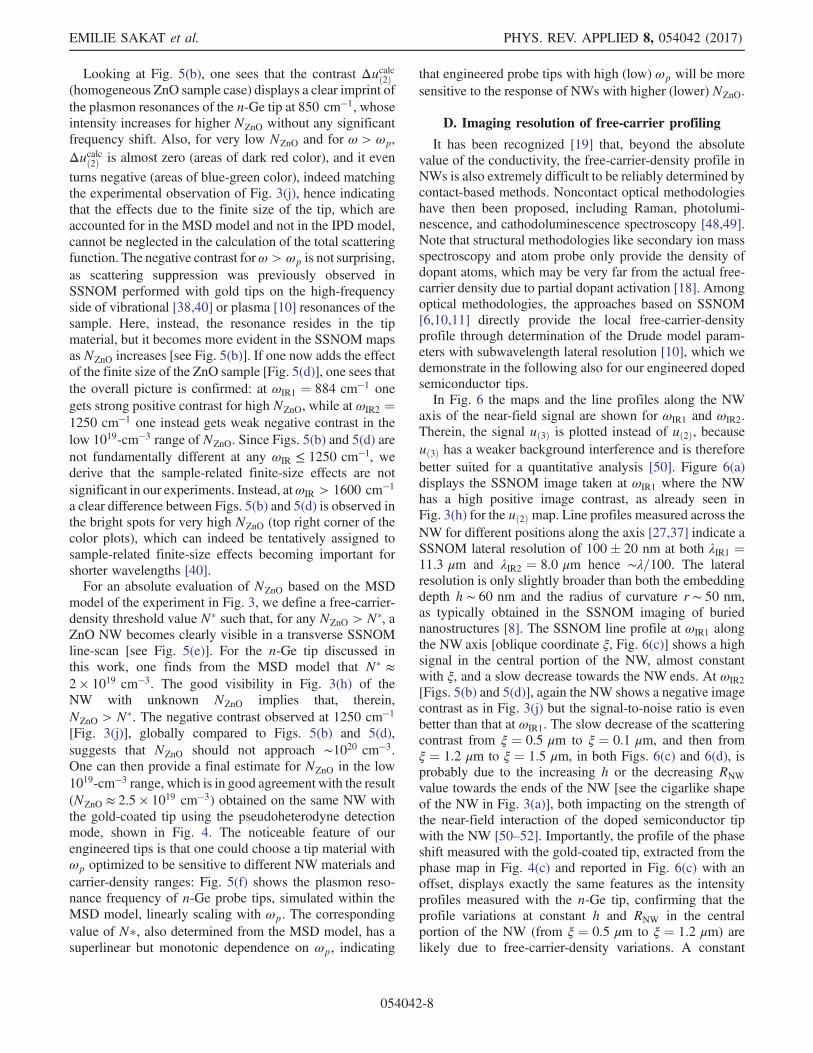
Looking at Fig. 5(b), one sees that the contrast Δucalcð2Þ(homogeneous ZnO sample case) displays a clear imprint ofthe plasmon resonances of the n-Ge tip at 850 cm−1, whoseintensity increases for higher NZnO without any significantfrequency shift. Also, for very low NZnO and for ω > ωp,Δucalcð2Þ is almost zero (areas of dark red color), and it even
turns negative (areas of blue-green color), indeed matchingthe experimental observation of Fig. 3(j), hence indicatingthat the effects due to the finite size of the tip, which areaccounted for in the MSD model and not in the IPD model,cannot be neglected in the calculation of the total scatteringfunction. The negative contrast forω > ωp is not surprising,as scattering suppression was previously observed inSSNOM performed with gold tips on the high-frequencyside of vibrational [38,40] or plasma [10] resonances of thesample. Here, instead, the resonance resides in the tipmaterial, but it becomes more evident in the SSNOM mapsas NZnO increases [see Fig. 5(b)]. If one now adds the effectof the finite size of the ZnO sample [Fig. 5(d)], one sees thatthe overall picture is confirmed: at ωIR1 ¼ 884 cm−1 onegets strong positive contrast for high NZnO, while at ωIR2 ¼1250 cm−1 one instead gets weak negative contrast in thelow 1019-cm−3 range of NZnO. Since Figs. 5(b) and 5(d) arenot fundamentally different at any ωIR ≤ 1250 cm−1, wederive that the sample-related finite-size effects are notsignificant in our experiments. Instead, atωIR > 1600 cm−1a clear difference between Figs. 5(b) and 5(d) is observed inthe bright spots for very high NZnO (top right corner of thecolor plots), which can indeed be tentatively assigned tosample-related finite-size effects becoming important forshorter wavelengths [40].For an absolute evaluation of NZnO based on the MSD
model of the experiment in Fig. 3, we define a free-carrier-density threshold value N� such that, for any NZnO > N�, aZnO NW becomes clearly visible in a transverse SSNOMline-scan [see Fig. 5(e)]. For the n-Ge tip discussed inthis work, one finds from the MSD model that N� ≈2 × 1019 cm−3. The good visibility in Fig. 3(h) of theNW with unknown NZnO implies that, therein,NZnO > N�. The negative contrast observed at 1250 cm−1[Fig. 3(j)], globally compared to Figs. 5(b) and 5(d),suggests that NZnO should not approach ∼1020 cm−3.One can then provide a final estimate for NZnO in the low1019-cm−3 range, which is in good agreement with the result(NZnO ≈ 2.5 × 1019 cm−3) obtained on the same NW withthe gold-coated tip using the pseudoheterodyne detectionmode, shown in Fig. 4. The noticeable feature of ourengineered tips is that one could choose a tip material withωp optimized to be sensitive to different NW materials andcarrier-density ranges: Fig. 5(f) shows the plasmon reso-nance frequency of n-Ge probe tips, simulated within theMSD model, linearly scaling with ωp. The correspondingvalue of N�, also determined from the MSD model, has asuperlinear but monotonic dependence on ωp, indicating
that engineered probe tips with high (low) ωp will be moresensitive to the response of NWs with higher (lower) NZnO.
D. Imaging resolution of free-carrier profiling
It has been recognized [19] that, beyond the absolutevalue of the conductivity, the free-carrier-density profile inNWs is also extremely difficult to be reliably determined bycontact-based methods. Noncontact optical methodologieshave then been proposed, including Raman, photolumi-nescence, and cathodoluminescence spectroscopy [48,49].Note that structural methodologies like secondary ion massspectroscopy and atom probe only provide the density ofdopant atoms, which may be very far from the actual free-carrier density due to partial dopant activation [18]. Amongoptical methodologies, the approaches based on SSNOM[6,10,11] directly provide the local free-carrier-densityprofile through determination of the Drude model param-eters with subwavelength lateral resolution [10], which wedemonstrate in the following also for our engineered dopedsemiconductor tips.In Fig. 6 the maps and the line profiles along the NW
axis of the near-field signal are shown for ωIR1 and ωIR2.Therein, the signal uð3Þ is plotted instead of uð2Þ, becauseuð3Þ has a weaker background interference and is thereforebetter suited for a quantitative analysis [50]. Figure 6(a)displays the SSNOM image taken at ωIR1 where the NWhas a high positive image contrast, as already seen inFig. 3(h) for the uð2Þ map. Line profiles measured across theNW for different positions along the axis [27,37] indicate aSSNOM lateral resolution of 100� 20 nm at both λIR1 ¼11.3 μm and λIR2 ¼ 8.0 μm hence ∼λ=100. The lateralresolution is only slightly broader than both the embeddingdepth h ∼ 60 nm and the radius of curvature r ∼ 50 nm,as typically obtained in the SSNOM imaging of buriednanostructures [8]. The SSNOM line profile at ωIR1 alongthe NW axis [oblique coordinate ξ, Fig. 6(c)] shows a highsignal in the central portion of the NW, almost constantwith ξ, and a slow decrease towards the NW ends. At ωIR2[Figs. 5(b) and 5(d)], again the NW shows a negative imagecontrast as in Fig. 3(j) but the signal-to-noise ratio is evenbetter than that at ωIR1. The slow decrease of the scatteringcontrast from ξ ¼ 0.5 μm to ξ ¼ 0.1 μm, and then fromξ ¼ 1.2 μm to ξ ¼ 1.5 μm, in both Figs. 6(c) and 6(d), isprobably due to the increasing h or the decreasing RNWvalue towards the ends of the NW [see the cigarlike shapeof the NW in Fig. 3(a)], both impacting on the strength ofthe near-field interaction of the doped semiconductor tipwith the NW [50–52]. Importantly, the profile of the phaseshift measured with the gold-coated tip, extracted from thephase map in Fig. 4(c) and reported in Fig. 6(c) with anoffset, displays exactly the same features as the intensityprofiles measured with the n-Ge tip, confirming that theprofile variations at constant h and RNW in the centralportion of the NW (from ξ ¼ 0.5 μm to ξ ¼ 1.2 μm) arelikely due to free-carrier-density variations. A constant
EMILIE SAKAT et al. PHYS. REV. APPLIED 8, 054042 (2017)
054042-8

NZnO is found along the NW axis, apart from a dip at theposition around ξ ¼ 0.8 μm, marked by stars in Figs. 6(c)and 6(d), which points towards a local depletion of thefree carriers, perhaps due to the presence of a structuralnucleation defect like the one visible in the inset ofFig. 6(d). This type of nucleation defect often correlatesto local suppression of the free-carrier density in ZnO NWsgrown with the hydrothermal method [53]. We notice that
the signal decrease at the NW ends and the dip at ξ ¼0.8 μm are identically seen at both ωIR1 and ωIR2, inde-pendently on the sign of the image contrast (positive forωIR1 < ωp and negative for ωIR2 > ωp), confirming thatthe doped semiconductor tip presented in this work featuresclear near-field interactions with the sample, both aboveand below its plasma frequency ωp, and is able to capturesmall local variations in NZnO.
III. CONCLUSIONS
Scanning near-field optical microscopy has been per-formed with purposely engineered doped semiconductortips featuring a plasma frequency in the midinfrared range.The intrinsic plasma resonance in the tip material (epitaxialheavily electron-doped germanium) provides a stronglywavelength-dependent scattering intensity contrast display-ing a clear correlation with the free-carrier density in ZnOnanowires with a very short Drude relaxation time. Thefree-carrier-density range of a single ZnO nanowire couldbe estimated by comparing the image contrast of the near-field microscopy maps acquired at two wavelengths, oneabove and one below the plasma wavelength of the tip, tothe image contrast calculated using a semianalytic multi-spherical dipole model of the near-field microscopy experi-ment. The results are positively benchmarked against thoseobtained with a conventional gold-coated tip in the moreprecise pseudoheterodyne detection mode, where bothphase and amplitude are measured. The model has alsoclarified that the shape and size of the doped semiconductortip strongly affect the scattering image contrast, while theshape and size of the nanowire have a lower impact. Ourdoped semiconductor tips therefore provide the same kindof information as that provided by the commonly usedgold-coated tips for specific SSNOM experiments. In thefuture, the monolithic fabrication of scanning probes madeof epitaxial material layers may open alternative avenues innear-field optical microscopy and scanning probe micros-copy in general.
ACKNOWLEDGMENTS
The authors acknowledge support fromAndreasHuber ofNeaspec GmbH, and wish to thank Shaul Aloni, VirginiaAltoe, Luca Businaro, Adele De Ninno, Giovanni Isella,Jacopo Frigerio, and Michele Celebrano for technical help.The work was partly funded by the Italian Ministry ofResearch through programs FIRB Futuro in Ricerca (GrantNo. RBFR08N9L9) and SIR (Grant No. RBSI14IT0D). Theresearch leading to these results has also received fundingfrom the EuropeanUnion’s Seventh Framework Programmeunder Grant No. 613055. Work at the Molecular Foundrywas supported by the Office of Science, Office of BasicEnergy Sciences, of the U.S. Department of Energy underContract No. DE-AC02-05CH11231, Molecular FoundryUser Proposal No. 1773.
FIG. 6. Assessment of the resolution of free-carrier profiling.(a),(b) Maps of the SNOM contrast of a ZnO nanowire (NW) overthe surrounding PDMS matrix observed at two IR frequencies. Inthe inset of (b) we show the SEM image of the same NW. (c),(d)SNOM signal profile cuts between the two NW extremitiesindicated by the black arrows in (a),(b) and by the yellow arrowsin the inset of (b). The abscissa of (c),(d) is the displacementcoordinate ξ along the NWaxis. The dashed green line representsthe average value of the contrast observed on the surroundingPDMS matrix. The lower end of the NW (ξ < 0.5 μm) is buriedunder a larger thickness of PDMS and it is not visible in thepresent SSNOMmaps and profiles. The pink curve in panel (c) isthe phase contrast profile measured with the gold-coated tip,extracted from Fig. 4(c). The pink curve is offset and scaled tomatch the red curve in the panel above. In panel (c), the highernoise level in the n-Ge tip profile (red curve) if compared to theAu tip (pink curve) is due to the higher mechanical noise of thenanoengineered tip. The stars in (c),(d) correspond to a positionwith slightly lower carrier density in the NW. This feature isattributed to the initial growth seed of the NW, with higher crystaldefect density. In the inset of panel (d), a SEM image of anothersimilar NW is shown, where the initial growth seed position isseen as a transversal indent in the middle of the NW.
NEAR-FIELD IMAGING OF FREE CARRIERS IN ZNO … PHYS. REV. APPLIED 8, 054042 (2017)
054042-9

APPENDIX: METHODS
Scanning probe tips made of doped semiconductors arefabricated by modifying commercial visible-apex siliconprobes (Nanosensors ATEC-NC) as described in Video 1.These tips had been previously used to perform AFMtopography imaging in contact and tapping mode, micro-photoluminescence emission, and SSNOM tests [27]. Theepitaxial germanium layers used in this work are grown onsilicon wafers by plasma-enhanced chemical vapor depo-sition using GeH4 and PH3 as gas precursors. A 2-μm-thickundoped Ge buffer layer is followed by the growth of a2-μm-thick electron-doped n-Ge layer with reduced defectdensity. The activated doping level n ≈ 2.5 × 1019 cm−3 isdetermined by Hall transport measurements [29]. Heavilyelectron-doped germanium has m� ¼ 0.12me, ε∞ ¼ 16,and with these values the plasma frequency can be predictedfrom the free-carrier density from ω2
p ¼ n=m�ε∞. Heavilydoped n-Ge films can nowadays be epitaxially grown infew-μm-thick layers perfectly suited for the fabrication ofscanning probe tips, and the value ofωp can bewidely tunedin themid-IR range up to about 2500 cm−1, as verified by IRspectroscopy on different semiconductor wafers [29].Electromagnetic simulations are conducted using a
commercial software (Lumerical Inc. FDTD Solutionsv8.9 software) for the FDTD data in Fig. 2 and with ahomemade code for Green’s function formalism [37] forthe MSD data in Fig. 5 [51]. The NW dielectric function iscalculated from the Drude model with parameters suitablefor ZnO: m� ¼ 0.29me, ε∞ ¼ 3.7, and different values ofN in the 1017–1020 cm−3 range. Illumination conditionsreplicate the Neaspec reflective objective at grazing inci-dence, with a 90° total horizontal opening angle, 20°vertical opening angle, and 60° incidence angle.ZnO nanowires are grown by the hydrothermal method
at 90 °C in an equimolar aqueous solution (5 mM) ofZnðNO3Þ26H2O and C6H12N4. Nanowires are immersed ina liquid solution of polydimethylisiloxane (PDMS) diluted1∶40 in n-heptane, which is then spun at 5000 rpm ontosilicon wafers and thermally cured on hotplate at 80 °C toform a conformal elastomeric matrix (thickness rangingfrom ∼60 nm on top of the NWs to 180 nm in the emptymatrix areas).SSNOM is performed with a scanning-sample AFM
where the tip is illuminated with a focused laser beam(neaSNOM by Neaspec GmbH). The laser systemsemployed in this work are a CO2 gas laser at 884 cm−1,and a quantum cascade laser with emission at 1250 cm−1.The detector of the backscattered radiation is a liquidnitrogen-cooled mercury and cadmium telluride (MCT)photovoltaic sensor. The scattered intensity signals uð2Þ,uð3Þ are amplified by lock-in demodulation at 2Ω and 3Ω,in order to isolate the contribution due to the near-fieldtip-sample interaction (Ω ∼ 70 kHz, cantilever chips byNanosensors, model ATEC-NC). Measurement on test
samples conducted with the n-Ge tip demonstrated thenear-field nature of the signal [37]. In order to maximizethe SSNOM contrast, the collection optics is aligned withthe tip on a position far from the NW, and ϕB is set tosmoothly vary around values close to 0 (i.e., the cosine termin Eq. (3) is maximized to smoothly vary around a valueclose to 1, considering that ϕS ≅ 0 on the weakly absorbingPDMS matrix). In this way, the problem of low-frequencymechanical noise of the n-Ge tip that prevents pseudohe-terodyne detection is partly circumvented. The pseudohe-terodyne detection is instead performed with a gold-coatedNanosensors ATEC-NC tip, with the Michelson interfer-ometer built into the neaSNOM microscope, with themoving mirror oscillating at 300 Hz.
[1] F. Keilmann and R. Hillenbrand, Near-field microscopy byelastic light scattering from a tip, Phil. Trans. R. Soc. A 362,787 (2004).
[2] N. Ocelic, A. Huber, and R. Hillenbrand, Pseudoheterodynedetection for background-free near-field spectroscopy,Appl. Phys. Lett. 89, 101124 (2006).
[3] M.M. Qazilbash, M. Brehm, B. G. Chae, P. C. Ho, G. O.Andreev, B. J. Kim, S. J. Yun, A. V. Balatsky, M. Maple,F. Keilmann, H. T. Kim, and D. N. Basov, Mott transition inVO2 revealed by infrared spectroscopy and nano-imaging,Science 318, 1750 (2007).
[4] A. J. Huber, F. Keilmann, J. Wittborn, J. Aizpurua, andR. Hillenbrand, Terahertz near-field nanoscopy of mobilecarriers in single semiconductor nanodevices, Nano Lett. 8,3766 (2008).
[5] E. A. Muller, B. Pollard, H. A. Bechtel, P. Van Blerkom,and M. B. Raschke, Infrared vibrational nanocrystallogra-phy and nanoimaging, Sci. Adv. 2, e1601006 (2016).
[6] M. Eisele, T. L. Cocker, M. A. Huber, M. Plankl, L. Viti, D.Ercolani, L. Sorba, M. S. Vitiello, and R. Huber, Ultrafastmulti-terahertz nano-spectroscopy with sub-cycle temporalresolution, Nat. Photonics 8, 841 (2014).
[7] Z. Shi, X. Hong, H. A. Bechtel, B. Zeng, M. C. Martin, K.Watanabe, T. Taniguchi, Y. Shen, and F. Wang, Observationof a Luttinger-liquid plasmon in metallic single-walledcarbon nanotubes, Nat. Photonics 9, 515 (2015).
[8] M. Wagner, A. S. McLeod, S. J. Maddox, Z. Fei, M. Liu,R. D. Averitt, M. Fogler, S. R. Bank, F. Keilmann, and D. N.Basov, Ultrafast dynamics of surface plasmons in inas bytime-resolved infrared nanospectroscopy, Nano Lett. 14,4529 (2014).
[9] J. M. Atkin, S. Berweger, A. C. Jones, and M. B. Raschke,Nano-optical imaging and spectroscopy of order, phases,and domains in complex solids, Adv. Phys. 61, 745 (2012).
[10] J. M. Stiegler, A. J. Huber, S. L. Diedenhofen, J. GómezRivas, R. E. Algra, E. P. A. M. Bakkers, and R. Hillenbrand,Nanoscale free-carrier profiling of individual semiconductornanowires by infrared near-field nanoscopy, Nano Lett. 10,1387 (2010).
[11] J. M. Stiegler, R. Tena-Zaera, O. Idigoras, A. Chuvilin, andR. Hillenbrand, Correlative infrared–electron nanoscopy
EMILIE SAKAT et al. PHYS. REV. APPLIED 8, 054042 (2017)
054042-10
reveals the local structure–conductivity relationship in zincoxide nanowires, Nat. Commun. 3, 1131 (2013).
[12] X. Duan, Y. Huang, Y. Cui, J. Wang, and C. M. Lieber,Indium phosphide nanowires as building blocks fornanoscale electronic and optoelectronic devices, Nature(London) 409, 66 (2001).
[13] D. Saxena, S. Mokkapati, P. Parkinson, N. Jiang, Q. Gao,H. H. Tan, and C. Jagadish, Optically pumped room-temperature gaas nanowire lasers, Nat. Photonics 7, 963(2013).
[14] X. Yang, A. Wolcott, G. Wang, A. Sobo, R. C. Fitzmorris, F.Qian, J. Z. Zhang, and Y. Li, Nitrogen-doped ZnO nanowirearrays for photoelectrochemical water splitting, Nano Lett.9, 2331 (2009).
[15] A. Janotti and C. G. Van de Walle, Fundamentals of zincoxide as a semiconductor, Rep. Prog. Phys. 72, 126501(2009).
[16] E. C. Garnett, Y. Tseng, D. R. Khanal, J. Wu, J. Bokor, andP. Yang, Dopant profiling and surface analysis of siliconnanowires using capacitance-voltage measurements, Nat.Nanotechnol. 4, 311 (2009).
[17] E. Koren, N. Berkovitch, and Y. Rosenwaks, Measurementof active dopant distribution and diffusion in individualsilicon nanowires, Nano Lett. 10, 1163 (2010).
[18] J. E. Allen, D. E. Perea, E. R. Hemesath, and L. J. Lauhon,Nonuniform nanowire doping profiles revealed by quanti-tative scanning photocurrent microscopy, Adv. Mater. 21,3067 (2009).
[19] H. J. Joyce, J. Boland, C. L. Davies, S. A. Baig, and M. B.Johnston, A review of the electrical properties of semi-conductor nanowires: Insights gained from terahertz con-ductivity spectroscopy, Semicond. Sci. Technol. 31, 103003(2016).
[20] D. Vanmaekelbergh and L. K. Van Vugt, ZnO nanowirelaser, Nanoscale 3, 2783 (2011).
[21] Z. L. Wang and J. Song, Piezoelectric nanogeneratorsbased on zinc oxide nanowire arrays, Science 312, 242(2006).
[22] Th. P. H. Sidiropoulos, R. Roder, S. Geburt, O. Hess, S. A.Maier, C. Ronning, and R. F. Oulton, Ultrafast plasmonicnanowire lasers near the surface plasmon frequency, Nat.Phys. 10, 870 (2014).
[23] J. B. Baxter and C. Schmuttenmaer, Conductivity of ZnOnanowires nanoparticles and thin films using time-resolvedterahertz spectroscopy, J. Phys. Chem. B 110, 25229 (2006).
[24] S. Kalusniak, S. Sadofev, and F. Henneberger, ZnO as aTunable Metal: New Types of Surface Plasmon Polaritons,Phys. Rev. Lett. 112, 137401 (2014).
[25] X. G. Xu, L. Gilburd, and G. C. Walker, Phase stabilizedhomodyne of infrared scattering type scanning near-fieldoptical microscopy, Appl. Phys. Lett. 105, 263104 (2014).
[26] X. G. Xu, A. E. Tanur, and G. C. Walker, Phase controlledhomodyne infrared near-field microscopy and spectroscopyreveal inhomogeneity within and among individual boronnitride nanotubes, J. Phys. Chem. A 117, 3348 (2013).
[27] V. Giliberti, E. Sakat, M. Bollani, M. V. P. Altoe, M. Melli,A. Weber-Bargioni, L. Baldassarre, M. Celebrano, J.Frigerio, G. Isella, S. Cabrini, and M. Ortolani, Function-alization of scanning probe tips with epitaxial semiconduc-tor layers, Small Methods 1, 1600033 (2017).
[28] F. Huth, A. Chuvilin, M. Schnell, I. Amenabar, P.Krutokhvostov, S. Lopatin, and R. Hillenbrand, Resonantantenna probes for tip-enhanced infrared near-field micros-copy, Nano Lett. 13, 1065 (2013).
[29] J. Frigerio, A. Ballabio, G. Isella, E. Sakat, G. Pellegrini,P. Biagioni, M. Bollani, E. Napolitani, C. Manganelli, M.Virgilio, A. Grupp, M. P. Fischer, D. Brida, K. Gallacher,D. J. Paul, L. Baldassarre, P. Calvani, V. Giliberti, A.Nucara, and M. Ortolani, Tunability of the dielectricfunction of heavily doped germanium thin films for mid-infrared plasmonics, Phys. Rev. B 94, 085202 (2016).
[30] L. Baldassarre, E. Sakat, J. Frigerio, A. Samarelli, K.Gallacher, E. Calandrini, G. Isella, D. J. Paul, M. Ortolani,and P. Biagioni, Midinfrared plasmon-enhanced spectros-copy with germanium antennas on silicon substrates, NanoLett. 15, 7225 (2015).
[31] M. Fleischer, A. Weber-Bargioni, M. V. P. Altoe, A.Schwartzberg, P. J. Schuck, S. Cabrini, and D. P. Kern,Gold nanocone near-field scanning optical microscopyprobes, ACS Nano 5, 2570 (2011).
[32] T. W. Johnson, Z. J. Lapin, R. Beams, N. C. Lindquist, S. G.Rodrigo, L. Novotny, and S. H. Oh, Highly reproduciblenear-field optical imaging with sub-20-nm resolution basedon template-stripped gold pyramids, ACS Nano 6, 9168(2012).
[33] F. De Angelis, G. Das, P. Candeloro, M. Patrini, M. Galli,A. Bek, M. Lazzarino, I. Maksymov, C. Liberale, L. C.Andreani, and E. Di Fabrizio, Nanoscale chemical mappingusing three-dimensional adiabatic compression of surfaceplasmon polaritons, Nat. Nanotechnol. 5, 67 (2010).
[34] W. Bao, M. Melli, N. Caselli, F. Riboli, D. S. Wiersma, M.Staffaroni, H. Choo, D. F. Ogletree, S. Aloni, J. Bokor, S.Cabrini, F. Intonti, M. B. Salmeron, E. Yablonovitch, P. J.Schuck, and A. Weber-Bargioni, Mapping local chargerecombination heterogeneity by multidimensional nano-spectroscopic imaging, Science 338, 1317 (2012).
[35] V. Giliberti, E. Sakat, L. Baldassarre, A. Di Gaspare, A.Notargiacomo, E. Giovine, J. Frigerio, G. Isella, M. Melli,A. Weber-Bargioni, S. Aloni, S. Sassolini, S. Cabrini, P.Biagioni, M. Ortolani, and M. Bollani, Three-dimensionalfabrication of free-standing epitaxial semiconductor nano-structures obtained by focused ion beam, Microelectron.Eng. 141, 168 (2015).
[36] Y. Zou, P. Steinvurzel, T. Yang, and K. B. Crozier, Surfaceplasmon resonances of optical antenna atomic force micro-scope tips, Appl. Phys. Lett. 94, 171107 (2009).
[37] See Supplemental Material at http://link.aps.org/supplemental/10.1103/PhysRevApplied.8.054042 for thedipole model formula, the details on the modelcomparison, and the lateral resolution of SSNOM withthe n-Ge tip.
[38] M. Brehm, T. Taubner, R. Hillenbrand, and F. Keilmann,Infrared spectroscopic mapping of single nanoparticles andviruses at nanoscale resolution, Nano Lett. 6, 1307 (2006).
[39] J. J. Greffet, A. Sentenac, and R. Carminati, Surface profilereconstruction using near-field data, Opt. Commun. 116, 20(1995).
[40] J. M. Stiegler, Y. Abate, A. Cvitkovic, Y. E. Romanyuk,A. J. Huber, S. R. Leone, and R. Hillenbrand, Nanoscaleinfrared absorption spectroscopy of individual nanoparticles
NEAR-FIELD IMAGING OF FREE CARRIERS IN ZNO … PHYS. REV. APPLIED 8, 054042 (2017)
054042-11

enabled by scattering-type near-field microscopy, ACSNano 5, 6494 (2011).
[41] R. Esteban, R. Vogelgesang, and K. Kern, Full simulationsof the apertureless scanning near field optical microscopysignal: achievable resolution and contrast, Opt. Express 17,2518 (2009).
[42] Z. H. Kim and S. H. Ahn, Nanometer-scale dielectricimaging of semiconductor nanoparticles: Size-dependentdipolar coupling and contrast reversal, Nano Lett. 7, 2258(2007).
[43] M. Esslinger and R. Vogelgesang, Reciprocity theory ofapertureless scanning near-field optical microscopy withpoint-dipole probes, ACS Nano 6, 8173 (2012).
[44] A. Cvitkovic, N. Ocelic, and R. Hillenbrand, Analyticalmodel for quantitative prediction of material contrasts inscattering-type near-field optical microscopy, Opt. Express15, 8550 (2007).
[45] A. S. McLeod, P. Kelly, M. D. Goldflam, Z. Gainsforth, A. J.Westphal, G. Dominguez, M. H. Thiemens, M.M. Fogler,and D. N. Basov, Model for quantitative tip-enhanced spec-troscopy and the extraction of nanoscale-resolved opticalconstants, Phys. Rev. B 90, 085136 (2014).
[46] B.-Y. Jiang, L. M. Zhang, A. H. Castro Neto, D. N. Basov,and M.M. Fogler, Generalized spectral method for near-field optical microscopy, J. Appl. Phys. 119, 054305 (2016).
[47] M. Langlais, J. P. Hugonin, M. Besbes, and P. Ben-Abdallah, Cooperative electromagnetic interactions between
nanoparticles for solar energy harvesting, Opt. Express 22,A577 (2014).
[48] D. Lindgren, O. Hultin, M. Heurlin, K. Storm, M. T.Borgström, L. Samuelson, and A. Gustafsson, Study ofcarrier concentration in single InP nanowires by lumines-cence and Hall measurements, Nanotechnology 26, 045705(2015).
[49] B. Ketterer, E. Uccelli, and A. Fontcuberta i Morral,Mobility and carrier density in p-type GaAs nanowiresmeasured by transmission Raman spectroscopy, Nanoscale4, 1789 (2012).
[50] A. A. Govyadinov, S. Mastel, F. Golmar, A. Chuvilin, P. S.Carney, and R. Hillenbrand, Recovery of permittivity anddepth from near-field data as a step toward infrared nano-tomography, ACS Nano 8, 6911 (2014).
[51] G. Wollny, E. Bründermann, Z. Arsov, L. Quaroni, and M.Havenith, Nanoscale depth resolution in scanning near-fieldinfrared microscopy, Opt. Express 16, 7453 (2008).
[52] A. P. Engelhardt, B. Hauer, and T. Taubner, Visibility ofweak contrasts in subsurface scattering near-field micros-copy, Ultramicroscopy 126, 40 (2013).
[53] Y. F. Hsu, Y. Y. Xi, K. H. Tam, A. B. Djurišić, J. Luo, C. C.Ling, C. K. Cheung, A. M. C. Ng, W. K. Chan, X. Deng,C. D. Beling, S. Fung, K. W. Cheah, P. W. K. Fong, andC. C. Surya, Undoped p-type ZnO nanorods synthesizedby a hydrothermal method, Adv. Funct. Mater. 18, 1020(2008).
EMILIE SAKAT et al. PHYS. REV. APPLIED 8, 054042 (2017)
054042-12