Embed Size (px)
Citation preview
Near-unity broadband absorption designs for semiconducting nanowire arrays via localized
radial mode excitation
Katherine T. Fountaine,1,2* Christian G. Kendall,2 and Harry A. Atwater 2,3 1Division of Chemistry & Chemical Engineering, California Institute of Technology, Pasadena, CA 91125, USA
2Joint Center for Artificial Photosynthesis, California Institute of Technology, Pasadena, CA 91125, USA 3Department of Applied Physics & Materials Science, California Institute of Technology, Pasadena, CA 91125, USA
Abstract: We report design methods for achieving near-unity broadband light absorption in sparse nanowire arrays, illustrated by results for visible absorption in GaAs nanowires on Si substrates. Sparse (<5% fill fraction) nanowire arrays achieve near unity absorption at wire resonant wavelengths due to coupling into ‘leaky’ radial waveguide modes of individual wires and wire-wire scattering processes. From a detailed conceptual development of radial mode resonant absorption, we demonstrate two specific geometric design approaches to achieve near unity broadband light absorption in sparse nanowire arrays: (i) introducing multiple wire radii within a small unit cell array to increase the number of resonant wavelengths, yielding a 15% absorption enhancement relative to a uniform nanowire array and (ii) tapering of nanowires to introduce a continuum of diameters and thus resonant wavelengths excited within a single wire, yielding an 18% absorption enhancement over a uniform nanowire array.
© 2014 Optical Society of America
OCIS codes: (160.6000) Semiconductor materials; (220.2740) Geometric optical design; (350.4238) Nanophotonics and photonic crystals; (350.6050) Solar energy.
References and links
1. L. Hu and G. Chen, “Analysis of optical absorption in silicon nanowire arrays for photovoltaic applications,” Nano Lett. 7(11), 3249–3252 (2007).
2. O. L. Muskens, J. G. Rivas, R. E. Algra, E. P. A. M. Bakkers, and A. Lagendijk, “Design of light scattering in nanowire materials for photovoltaic applications,” Nano Lett. 8(9), 2638–2642 (2008).
3. P. Spinelli, M. A. Verschuuren, and A. Polman, “Broadband omnidirectional antireflection coating based on subwavelength surface Mie resonators,” Nat Commun 3(692), 692 (2012).
4. C. Lin and M. L. Povinelli, “Optical absorption enhancement in silicon nanowire arrays with a large lattice constant for photovoltaic applications,” Opt. Express 17(22), 19371–19381 (2009).
5. J. Li, H. Yu, S. M. Wong, X. Li, G. Zhang, P. G. Lo, and D. L. Kwong, “Design guidelines of periodic Si nanowire arrays for solar cell application,” Appl. Phys. Lett. 95(243113), 1–3 (2009).
6. L. Wen, Z. Zhao, X. Li, Y. Shen, H. Guo, and Y. Wang, “Theoretical analysis and modeling of light trappig in high efficiency GaAs nanowire array solar cells,” Appl. Phys. Lett. 99(143116), 1–3 (2011).
7. Z. Fan, R. Kapadia, P. W. Leu, X. Zhang, Y. L. Chueh, K. Takei, K. Yu, A. Jamshidi, A. A. Rathore, D. J. Ruebusch, M. Wu, and A. Javey, “Ordered arrays of dual-diameter nanopillars for maximized optical absorption,” Nano Lett. 10(10), 3823–3827 (2010).
8. L. Cao, J. S. White, J. S. Park, J. A. Schuller, B. M. Clemens, and M. L. Brongersma, “Engineering light absorption in semiconductor nanowire devices,” Nat. Mater. 8(8), 643–647 (2009).
9. S. K. Kim, R. W. Day, J. F. Cahoon, T. J. Kempa, K. D. Song, H. G. Park, and C. M. Lieber, “Tuning Light Absorption in core/shell silicon nanowire photovoltaic devices through morphological design,” Nano Lett. 12(9), 4971–4976 (2012).
10. K. Seo, M. Wober, P. Steinvurzel, E. Schonbrun, Y. Dan, T. Ellenbogen, and K. B. Crozier, “Multicolored Vertical Silicon Nanowires,” Nano Lett. 11(4), 1851–1856 (2011).
11. B. Kayes, H. A. Atwater, and N. S. Lewis, “Comparison of the device physics principles of planar and radial p-n junction nanorod solar cells,” J. Appl. Phys. 97(114302), 1–11 (2005).
12. E. Garnett and P. Yang, “Light trapping in silicon nanowire solar cells,” Nano Lett. 10(3), 1082–1087 (2010).
#206157 - $15.00 USD Received 10 Feb 2014; revised 6 Apr 2014; accepted 6 Apr 2014; published 18 Apr 2014(C) 2014 OSA 5 May 2014 | Vol. 22, No. S3 | DOI:10.1364/OE.22.00A930 | OPTICS EXPRESS A930
13. L. Cao, P. Fan, A. P. Vasudev, J. S. White, Z. Yu, W. Cai, J. A. Schuller, S. Fan, and M. L. Brongersma, “Semiconductor nanowire optical antenna solar absorbers,” Nano Lett. 10(2), 439–445 (2010).
14. M. D. Kelzenberg, S. W. Boettcher, J. A. Petykiewicz, D. B. Turner-Evans, M. C. Putnam, E. L. Warren, J. M. Spurgeon, R. M. Briggs, N. S. Lewis, and H. A. Atwater, “Enhanced absorption and carrier collection in Si wire arrays for photovoltaic applications,” Nat. Mater. 9(3), 239–244 (2010).
15. J. Kupec and B. Witzigmann, “Dispersion, wav propagation and efficiency analysis of nanowire solar cells,” Opt. Exp. 17(12), 10399–10410 (2009).
16. R. R. LaPierre, “Theoretical conversion efficiency of a two-junction III-V nanowire on Si solar cell,” J. Appl. Phys. 109(014310), 1–6 (2011).
17. E. Ertekin, P. A. Greaney, D. C. Chrzan, and T. D. Sands, “Equilibrium limits of coherency in strained nanowire heterostructures,” J. Appl. Phys. 97(114325), 1–10 (2005).
18. L. C. Chuang, M. Moewe, C. Chase, N. P. Kobayashi, C. Chang-Hasnain, and S. Crankshaw, “Critical diameter for III-V nanowires grown on lattice mismatched substrates,” Appl. Phys. Lett. 90(043115), 1–3 (2007).
19. M. Heiss, E. Russo-Averchi, A. Dalmau-Mallorquí, G. Tütüncüoğlu, F. Matteini, D. Rüffer, S. Conesa-Boj, O. Demichel, E. Alarcon-Lladó, and A. Fontcuberta i Morral, “III-V nanowire arrays: growth and light interaction,” Nanotechnology 25(1), 014015 (2014).
20. J. Noborisaka, J. Motohisa, and T. Fukui, “Catalyst-free growth of GaAs nanowires by selective-area metalorganic vapor-phase epitaxy,” Appl. Phys. Lett. 86(213102), 1–3 (2005).
21. G. Mariani, P. S. Wong, A. M. Katzenmeyer, F. Léonard, J. Shapiro, and D. L. Huffaker, “Patterned radial GaAs nanopillar solar cells,” Nano Lett. 11(6), 2490–2494 (2011).
22. T. Mårtensson, P. Carlberg, M. Borgstrom, L. Montelius, W. Seifert, and L. Samuelson, “Nanowire arrays defined by nanoimprint lithography,” Nano Lett. 4(4), 699–702 (2004).
23. A. Deinega and S. John, “Solar power conversion efficiency in modulated silicon nanowire photonic crystals,” J. Appl. Phys. 112(074327), 1–7 (2012).
24. L. Hong, X. Rusli, H. Wang, H. Zheng, and H. Y. Yu, “Design guidelines for slanting silicon nanowire arrays for solar cell application,” J. Appl. Phys. 114(084303), 1–6 (2013).
25. A. Chutinan and S. John, “Light trapping and absorption optimization in certain thin-film photonic crystal architectures,” Phys. Rev. A 78(023825), 1–15 (2008).
26. B. C. P. Sturmberg, K. B. Dossou, L. C. Botten, A. A. Asatryan, C. G. Poulton, C. M. de Sterke, and R. C. McPhedran, “Modal analysis of enhanced absorption in silicon nanowire arrays,” Opt. Express 19(S5 Suppl 5), A1067–A1081 (2011).
27. S. Hu, C. Chi, K. T. Fountaine, M. Yao, H. A. Atwater, P. D. Dapkus, N. S. Lewis, and C. Zhou, “Optical, electrical, and solar energy-conversion properties of gallium arsenide nanowire-array photoanodes,” Energy Environ. Sci. 6(6), 1879–1890 (2013).
28. G. Grzela, R. Paniagua-Domínguez, T. Barten, Y. Fontana, J. A. Sánchez-Gil, and J. Gómez Rivas, “Nanowire antenna emission,” Nano Lett. 12(11), 5481–5486 (2012).
29. Y. Yu and L. Cao, “Coupled leaky mode theory for light absorption in 2D, 1D, and 0D semiconductor nanostructures,” Opt. Express 20(13), 13847–13856 (2012).
30. Y. M. Chang, J. Shieh, and J. Y. Juang, “Subwavelength antireflective Si nanostructures fabricated by using the self-assembled silver metal-nanomask,” J. Phys. Chem. C 115(18), 8983–8987 (2011).
31. S. Patchett, M. Khorasaninejad, O. Nixon, and S. S. Saini, “Effective index approximation for ordered silicon nanowire arrays,” JOSA B 30(2), 306–313 (2013).
32. E. Yablonovitch, “Statistical ray optics,” J. Opt. Soc. Am. 72(7), 899–907 (1982). 33. Z. Yu, A. Raman, and S. Fan, “Fundamental limit of nanophotonic light trapping in solar cells,” Proc. Natl.
Acad. Sci. U.S.A. 107(41), 17491–17496 (2010). 34. D. M. Callahan, J. N. Munday, and H. A. Atwater, “Solar cell light trapping beyond the ray optic limit,” Nano
Lett. 12(1), 214–218 (2012). 35. S. L. Diedenhofen, O. T. A. Janssen, G. Grzela, E. P. A. M. Bakkers, and J. Gómez Rivas, “Strong geometrical
dependence of the absorption of light in arrays of semiconductor nanowires,” ACS Nano 5(3), 2316–2323 (2011).
36. H. Cansizoglu, M. F. Cansizoglu, M. Finckenor, and T. Karabacak, “Optical absorption properties of semiconducting nanostructures with different shapes,” Adv. Opt. Mat. 1(2), 158–166 (2013).
37. D. M. Callahan, K. A. W. Horowitz, and H. A. Atwater, “Light trapping in ultrathin silicon photonic cristal superlattices with randomly-textured dielectric incouplers,” Opt. Exp. 21(25), 30315–30326 (2013).
38. C. X. Lin, N. F. Huang, and M. L. Povinelli, “Effect of aperiodicity on the broadhand reflection of silicon nanorod structures for photovoltaics,” Opt. Exp. 20(S1), A125–A132 (2012).
39. K. Vynck, M. Burresi, F. Riboli, and D. S. Wiersma, “Photon management in two-dimensional disordered media,” Nat. Mater. 11(12), 1017–1022 (2012).
40. K. X. Wang, Z. Yu, V. Liu, Y. Cui, and S. Fan, “Absorption enhancement in ultrathin crystalline silicon solar cells with antireflection and light-trapping nanocone gratings,” Nano Lett. 12(3), 1616–1619 (2012).
41. B. C. P. Sturmberg, K. B. Dossou, L. C. Botten, A. A. Asatryan, C. G. Poulton, R. C. McPhedran, and C. Martijn de Sterke, “Nanowire array photovoltaics: radial disorder versus design for optimal efficiency,” Appl. Phys. Lett. 101(173902), 1–4 (2012).
42. H. Alaeian, A. C. Atre, and J. A. Dionne, “Optimized light absorption in Si wire array solar cells,” J. Opt. 14(024006), 1–6 (2012).
#206157 - $15.00 USD Received 10 Feb 2014; revised 6 Apr 2014; accepted 6 Apr 2014; published 18 Apr 2014(C) 2014 OSA 5 May 2014 | Vol. 22, No. S3 | DOI:10.1364/OE.22.00A930 | OPTICS EXPRESS A931
43. J. Y. Jung, Z. Guo, S. W. Jee, H. D. Um, K. T. Park, and J. H. Lee, “A strong antireflective solar cell prepared by tapering silicon nanowires,” Opt. Express 18(S3 Suppl 3), A286–A292 (2010).
44. M. A. Green, K. Emery, Y. Hishikawa, W. Warta, and E. D. Dunlop, “Solar cell efficiency tables (version 42),” Prog. Photovolt. Res. Appl. 21(1), 827–837 (2013).
45. P. Mohan, J. Motohisa, and T. Fukui, “Controlled growth of highly uniform, axial/radial direction-defined, individually addressable InP nanowire arrays,” Nanotech. 16(12), 2903–2907 (2005).
1. Introduction and motivation
In recent years, photonic phenomena in semiconductor nanowires have been the subject of great interest and intensive research effort, motivated by fundamental interest owing to their remarkable optical properties, including reduced reflectance [1–3], increased absorption [4–7], and spectral selectivity [8–10], and are also of considerable interest in applications to optoelectronic and photovoltaic devices. For next generation photovoltaics, arrays of semiconducting nanowires present an opportunity to reduce material usage and cost, while maintaining or improving optoelectronic performance relative to thin film or bulk materials. In particular nanowires can exhibit light trapping features not seen in thin films and also have the potential to orthogonalize the directions of light absorption and carrier collection, which enhances carrier collection in materials with short carrier diffusion lengths [11–16]. In addition to offering new optical design features, nanowires also relax the constraints imposed by lattice-matching requirements via radial strain relaxation [17,18], enabling high quality, single crystalline, nanowire growth on lattice-mismatched substrates. Nanowire arrays with a wide range of materials, wire diameters and arrays densities have been investigated experimentally and theoretically. In particular, high fidelity arrays of III-V nanowires can be fabricated via molecular beam epitaxy (MBE) [19] or metalorganic chemical vapor deposition (MOCVD), using either the selective-area growth (SAG, catalyst-free) [20,21] or vapor-liquid-solid (VLS, typically Au catalyst) methods [22]. The array pitch and wire diameter are easily tunable due to the use of patterned masks, created by electron-beam lithography [20] or nanoimprint lithography [22]. Reported light trapping mechanisms include coupling into photonic crystal modes [4, 23–26], coupling into leaky radial waveguide modes [8,13,15,27–29], and absorption in media considered using effective index models [30,31]. In this paper, we discuss mechanisms for broadband absorption in sparse arrays, where light coupling into localized radial modes dominates over coupling into Bloch-like photonic crystal modes that depend on array periodicity. In the present work, the sparsity of the array (5% fill fraction) results in very minimal coupling between nanowires, so an analysis based on localized resonant modes rather than a Bloch analysis is more appropriate and is thus used here.
An ideal solar cell would exhibit near unity absorption across the entire ultraviolet/visible spectrum up to its bandgap. State-of-the-art GaAs solar cells with thicknesses exceeding several microns can achieve near unity broadband absorption in the blue and mid-visible wavelength range, but exhibit incomplete light absorption for wavelengths near the semiconductor bandgap. In principle, resonant absorption in nanostructures via sub-wavelength light trapping phenomena, such as leaky radial waveguide mode absorption, can exceed the Lambertian absorption limit over a narrow wavelength range near resonance [10,32–34]. However, owing to the discrete nature of resonant modes in nanowires, achieving near-unity broadband absorption is challenging and is not possible in sparse wire arrays with uniform diameter. Therefore, in order for nanostructured devices to compete with current state-of-the-art planar cells in photovoltaic conversion efficiency, optical design methods can be employed to increase the number of resonances and the wavelength range for resonant mode excitation, given the inherently spectrally-dependent resonant characteristics of nanowire radial modes. Previous reports on nanowire arrays have demonstrated the ability to alter nanowire array light absorption with geometric modification of nanowire diameter, shape and order [7,19,23,24,35–43]. Specifically, the anti-reflective properties of tapering silicon nanowires have been discussed theoretically [42] and demonstrated experimentally [43]. Our work extends the scope of these studies by developing an analysis of the absorption
#206157 - $15.00 USD Received 10 Feb 2014; revised 6 Apr 2014; accepted 6 Apr 2014; published 18 Apr 2014(C) 2014 OSA 5 May 2014 | Vol. 22, No. S3 | DOI:10.1364/OE.22.00A930 | OPTICS EXPRESS A932
enhancement in tapered nanowires in the context of resonant modal absorption. Here we take a directed approach to geometric optimization of nanowire arrays, guided by the theory of localized mode excitation in nanowires, to achieve near unity broadband absorption in sparse arrays. We propose two simple pathways to achieving a broadband enhancement in nanowire array light absorption: (i) introducing multiple wire radii within a small unit cell array to increase the number of resonant wavelengths and (ii) tapering nanowires to introduce a continuum of diameters and resonant wavelengths within a single wire.
The design principles and methods are discussed in the context of GaAs nanowires on a Si substrate, but are generally applicable to any sparse array of semiconducting nanowires where radial leaky modes are the primary mechanism responsible for resonant absorption. Because a primary concern for GaAs- and other III-V material-based photovoltaics is material cost, an equal material usage constraint is applied to the array optimizations. Additionally, an equal material usage comparison highlights differences in absorption/volume, and thus, underscores the effects of the modal resonances for varying geometries. Consequently, all designs discussed have a 5% fill fraction and a constant nanostructure height of 3 µm, corresponding to a 150 nm planar equivalent thickness.
2. Results and discussion
2.1 Uniform nanowire arrays
Previously, we reported the very strong light absorption properties of sparse (<5% fill fraction) GaAs nanowire arrays grown on both GaAs and Si substrates via selective area growth MOCVD, supported by experiments, simulations and analytical theory [27]. We focus our design in the range of wire geometries employed in this previous study and investigate the simulated wavelength-dependent absorption for a 5% fill fraction, uniform array of GaAs nanowires with heights of 3 µm and radii of 65 nm, which is shown in (red) in Fig. 1. The absorption ranges from 60 to 100% in the wire arrays and integrates to an absorbed current of 25.0 mA/cm2, far exceeding the absorbed current of 10.5 mA/cm2 in a planar equivalent material volume (thickness = 150 nm). This strong absorption, despite the low fill fraction, is explained by coupling into resonant ‘leaky’ radial waveguide modes, which are electromagnetic modes with enhanced electric and magnetic field intensities localized on the nanowire. The spectral positions of the modal resonances depend only on radius and are independent of array period, leading to the denotation of the modes as radial modes. The eigenvalue equation for an individual, infinitely long cylinder shown below [Eq. (1)], as determined from Maxwell’s equations for a lossless, dielectric medium, determines the resonant wavelengths for each leaky mode, where a is the wire radius, k0 and β are the total and z-component of the wave vector in free space, k1 (k2) and n1 (n2) are the transverse components of the wave vectors and refractive indices inside(outside) the nanowire, and Jm, Km, and Hm are the Bessel (1st kind), modified Bessel (2nd kind), and Hankel (1st kind) functions. Leaky mode resonances occur at β = 0, leading the first term on the right hand side of the equation to give the transverse magnetic (TM) modes and the second term to give the transverse electric (TE) modes.
( )( )
( )( )
( )( )
( )( )
22 ' ' ' '2 21 2 1 21 2
2 20 1 1 2 2 1 1 2 21 2
1 1 1m m m m
m m m m
J k a H k a J k a H k an nm
k a k J k a k H k a k J k a k H k ak k
β = − − −
(1)
Note that this eigenvalue equation, and hence the eigenmodes, essentially depends only on nanowire radius, material refractive indices, and the wavelength of incident light. Eigenmode notation is written as TMmn or TEmn, where m and n are the azimuthal and radial mode numbers, indicating the number of field maxima in a given direction. Specifically, in the previous work, the TM11 and TM12 modes, as determined from Eq. (1), were identified as the modes responsible for the resonant absorption peaks of nanowire arrays. In this array
#206157 - $15.00 USD Received 10 Feb 2014; revised 6 Apr 2014; accepted 6 Apr 2014; published 18 Apr 2014(C) 2014 OSA 5 May 2014 | Vol. 22, No. S3 | DOI:10.1364/OE.22.00A930 | OPTICS EXPRESS A933
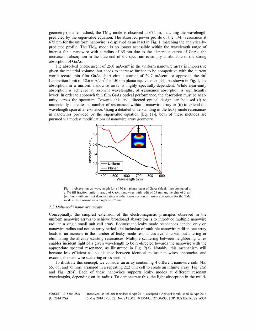
geometry (smaller radius), the TM11 mode is observed at 675nm, matching the wavelength predicted by the eigenvalue equation. The absorbed power profile of the TM11 resonance at 675 nm for the uniform nanowire is displayed as an inset in Fig. 1, matching the analytically-predicted profile. The TM12 mode is no longer accessible within the wavelength range of interest for a nanowire with a radius of 65 nm due to the dispersion curve of GaAs; the increase in absorption in the blue end of the spectrum is simply attributable to the strong absorption of GaAs.
The absorbed photocurrent of 25.0 mA/cm2 in the uniform nanowire array is impressive given the material volume, but needs to increase further to be competitive with the current world record thin film GaAs short circuit current of 29.7 mA/cm2 or approach the 4n2 Lambertian limit of 32.6 mA/cm2 for 150 nm planar equivalence [44]. As shown in Fig. 1, the absorption in a uniform nanowire array is highly spectrally-dependent. While near-unity absorption is achieved at resonant wavelengths, off-resonance absorption is significantly lower. In order to approach thin film GaAs optical performance, the absorption must be near-unity across the spectrum. Towards this end, directed optical design can be used (i) to numerically increase the number of resonances within a nanowire array or (ii) to extend the wavelength span of a resonance. Using a detailed understanding of the leaky mode resonances in nanowires provided by the eigenvalue equation [Eq. (1)], both of these methods are pursued via modest modifications of nanowire array geometry.
Fig. 1. Absorption vs. wavelength for a 150 nm planar layer of GaAs (black line) compared to a 5% fill fraction uniform array of GaAs nanowires with radii of 65 nm and heights of 3 µm (red line) with an inset demonstrating a radial cross section of power absorption for the TM11 mode at its resonant wavelength of 675 nm
2.2 Multi-radii nanowire arrays
Conceptually, the simplest extension of the electromagnetic principles observed in the uniform nanowire arrays to achieve broadband absorption is to introduce multiple nanowire radii in a single small unit cell array. Because the leaky mode resonances depend only on nanowire radius and not on array period, the inclusion of multiple nanowire radii in one array leads to an increase in the number of leaky mode resonances available without altering or eliminating the already existing resonances. Multiple scattering between neighboring wires enables incident light of a given wavelength to be re-directed towards the nanowire with the appropriate spectral resonance, as illustrated in Fig. 2(a). Notably, this mechanism will become less efficient as the distance between identical radius nanowires approaches and exceeds the nanowire scattering cross section.
To illustrate this concept, we consider an array containing 4 different nanowire radii (45, 55, 65, and 75 nm), arranged in a repeating 2x2 unit cell to create an infinite array [Fig. 2(a) and Fig. 2(b)]. Each of these nanowires supports leaky modes at different resonant wavelengths, depending on its radius. To demonstrate this, the light absorption in the multi-
#206157 - $15.00 USD Received 10 Feb 2014; revised 6 Apr 2014; accepted 6 Apr 2014; published 18 Apr 2014(C) 2014 OSA 5 May 2014 | Vol. 22, No. S3 | DOI:10.1364/OE.22.00A930 | OPTICS EXPRESS A934
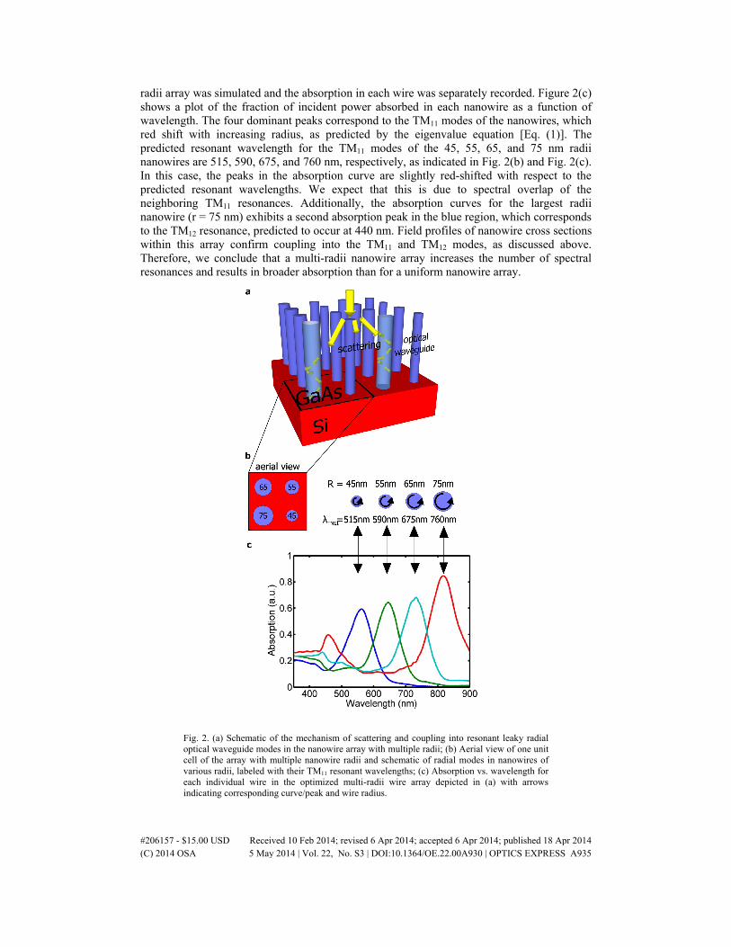
radii array was simulated and the absorption in each wire was separately recorded. Figure 2(c) shows a plot of the fraction of incident power absorbed in each nanowire as a function of wavelength. The four dominant peaks correspond to the TM11 modes of the nanowires, which red shift with increasing radius, as predicted by the eigenvalue equation [Eq. (1)]. The predicted resonant wavelength for the TM11 modes of the 45, 55, 65, and 75 nm radii nanowires are 515, 590, 675, and 760 nm, respectively, as indicated in Fig. 2(b) and Fig. 2(c). In this case, the peaks in the absorption curve are slightly red-shifted with respect to the predicted resonant wavelengths. We expect that this is due to spectral overlap of the neighboring TM11 resonances. Additionally, the absorption curves for the largest radii nanowire (r = 75 nm) exhibits a second absorption peak in the blue region, which corresponds to the TM12 resonance, predicted to occur at 440 nm. Field profiles of nanowire cross sections within this array confirm coupling into the TM11 and TM12 modes, as discussed above. Therefore, we conclude that a multi-radii nanowire array increases the number of spectral resonances and results in broader absorption than for a uniform nanowire array.
Fig. 2. (a) Schematic of the mechanism of scattering and coupling into resonant leaky radial optical waveguide modes in the nanowire array with multiple radii; (b) Aerial view of one unit cell of the array with multiple nanowire radii and schematic of radial modes in nanowires of various radii, labeled with their TM11 resonant wavelengths; (c) Absorption vs. wavelength for each individual wire in the optimized multi-radii wire array depicted in (a) with arrows indicating corresponding curve/peak and wire radius.
#206157 - $15.00 USD Received 10 Feb 2014; revised 6 Apr 2014; accepted 6 Apr 2014; published 18 Apr 2014(C) 2014 OSA 5 May 2014 | Vol. 22, No. S3 | DOI:10.1364/OE.22.00A930 | OPTICS EXPRESS A935
2.3 Nanocone arrays
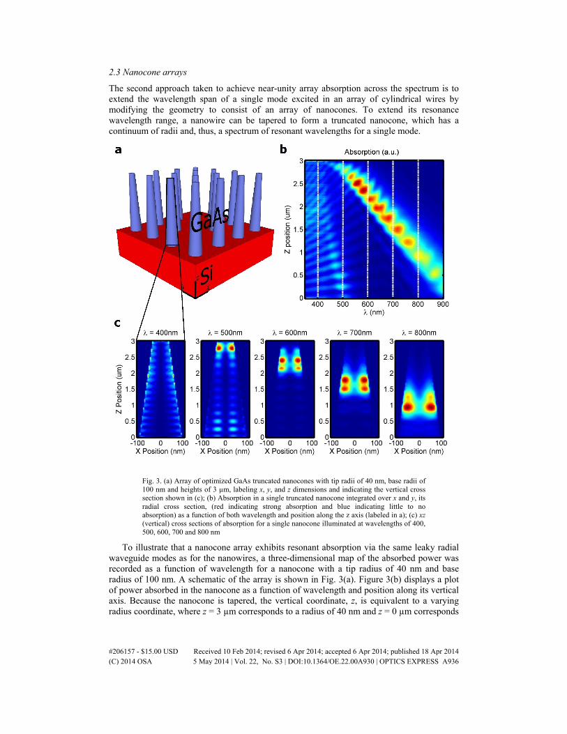
The second approach taken to achieve near-unity array absorption across the spectrum is to extend the wavelength span of a single mode excited in an array of cylindrical wires by modifying the geometry to consist of an array of nanocones. To extend its resonance wavelength range, a nanowire can be tapered to form a truncated nanocone, which has a continuum of radii and, thus, a spectrum of resonant wavelengths for a single mode.
Fig. 3. (a) Array of optimized GaAs truncated nanocones with tip radii of 40 nm, base radii of 100 nm and heights of 3 µm, labeling x, y, and z dimensions and indicating the vertical cross section shown in (c); (b) Absorption in a single truncated nanocone integrated over x and y, its radial cross section, (red indicating strong absorption and blue indicating little to no absorption) as a function of both wavelength and position along the z axis (labeled in a); (c) xz (vertical) cross sections of absorption for a single nanocone illuminated at wavelengths of 400, 500, 600, 700 and 800 nm
To illustrate that a nanocone array exhibits resonant absorption via the same leaky radial waveguide modes as for the nanowires, a three-dimensional map of the absorbed power was recorded as a function of wavelength for a nanocone with a tip radius of 40 nm and base radius of 100 nm. A schematic of the array is shown in Fig. 3(a). Figure 3(b) displays a plot of power absorbed in the nanocone as a function of wavelength and position along its vertical axis. Because the nanocone is tapered, the vertical coordinate, z, is equivalent to a varying radius coordinate, where z = 3 µm corresponds to a radius of 40 nm and z = 0 µm corresponds
#206157 - $15.00 USD Received 10 Feb 2014; revised 6 Apr 2014; accepted 6 Apr 2014; published 18 Apr 2014(C) 2014 OSA 5 May 2014 | Vol. 22, No. S3 | DOI:10.1364/OE.22.00A930 | OPTICS EXPRESS A936
to a radius of 100nm. The largely red diagonal peak stretching from z = 0 µm and λ ~900 nm up to z = 3 µm and λ ~500 nm, the most prominent feature of Fig. 3(b), is the absorption into the resonant TM11 mode. To confirm coupling into the TM11 mode of the nanocone, radial cross sections of the absorbed power at the resonant wavelength-radius pairs indicated by the prominent diagonal peak in Fig. 3(b) were observed and found to match that of TM11 modes. Additionally, these wavelength-radius pairs match the eigenvalues predicted by Eq. (1). In addition to the strong TM11 peak observed in Fig. 3(b), a second, fainter diagonal peak is visible stretching from z = 0 µm and λ ~500 nm up to z ~1.5 µm and λ ~450 nm. The TM12 mode is responsible for this resonant absorption. The peak slowly fades away for larger z as the nanocone radius decreases and ultimately disappears around r = 70 nm (or z = 1.5 µm) where the mode is no longer accessible due to the dispersion curve of GaAs. The diagonal character of both the TM11 and TM12 peaks demonstrates that these modes have a spectrum of resonant wavelengths in a nanocone, as intended.
Another interesting feature of Fig. 3(b) is the sinusoidal variation of the absorbed power along the z axis. This modulation in absorption is due to longitudinal resonances, and the overall absorbed power intensity profile of Fig. 3(b) is explained by a linear combination of longitudinal resonances and radial resonances. This phenomenon is more clearly discernible from xz cross sections of the power absorbed in a nanocone, displayed in Fig. 3(c) for wavelengths of 400, 500, 600, 700, and 800 nm. All five of these cross sections illustrate the longitudinal modes present in the nanocone which give rise to the characteristic vertical oscillations in absorption intensity. Focusing on the four longer wavelength cross sections, the radial TM11 resonance shifts downward to larger radius with increasing wavelength and has multiple lobes in the vertical direction due to its convolution with the longitudinal resonances. No strong radial mode is visible for the 400 nm wavelength cross section because GaAs absorbs strongly in this region and light does not penetrate deep enough into the nanocone to establish a radial mode. Additionally, in the 500 nm wavelength cross section, the character of the TM12 mode is visible at the bottom of the nanocone, as an additional radial absorption peak becomes visible at the rim of the nanocone. From this detailed analysis of nanocone absorption, we conclude that arrays of truncated nanocones exhibit spectrally-extended resonances and provide another method to achieving a more broadband optical absorption response in nanowire arrays.
2.4 Optimization
Using the conceptual understanding developed above, directed optimization using modest geometric modifications can be employed to realize broadband light absorption in nanowire arrays. Schematics of the optimized structures along with their power absorption profiles for a 65 nm radii nanowire cross section (λres = 675 nm) and their absorption curves are shown in Fig. 4(a), Fig. 4(b), and Fig. 4(c), respectively. The side-by-side display of the power absorption cross sections [Fig. 4(b)] in each optimized structure underscores their essentially identical TM11 modal characteristic.
As previously mentioned, the optimizations were performed under the constraint of constant fill fraction (5%) and constant nanostructure height (3 µm), corresponding to a 150 nm planar equivalent thin film. For comparison, the planar equivalent thin film absorbs 10.5 mA/cm2 and the uniform array of 65 nm radius nanowires [Fig. 4(a)] absorbs 25.0 mA/cm2. The absorption curves for these cases are displayed in Fig. 1 and Fig. 4(c) as the black and red lines, respectively. Note that partial spectral averaging has been used for the planar layer to smooth out the Fabry-Perot resonances (see Methods for details). All nanostructures are positioned on top of an infinite Si substrate and embedded in a 30 nm layer of SiOx to emulate SAG-MOCVD as-grown structures [27].
#206157 - $15.00 USD Received 10 Feb 2014; revised 6 Apr 2014; accepted 6 Apr 2014; published 18 Apr 2014(C) 2014 OSA 5 May 2014 | Vol. 22, No. S3 | DOI:10.1364/OE.22.00A930 | OPTICS EXPRESS A937
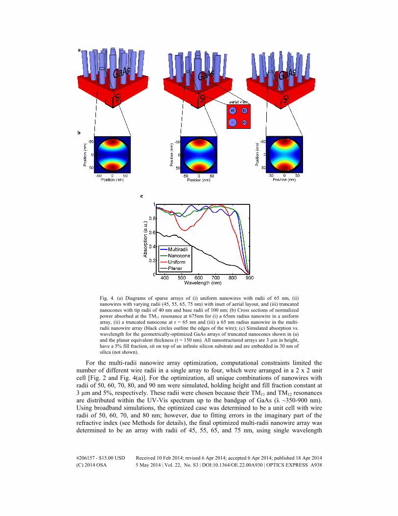
Fig. 4. (a) Diagrams of sparse arrays of (i) uniform nanowires with radii of 65 nm, (ii) nanowires with varying radii (45, 55, 65, 75 nm) with inset of aerial layout, and (iii) truncated nanocones with tip radii of 40 nm and base radii of 100 nm; (b) Cross sections of normalized power absorbed at the TM11 resonance at 675nm for (i) a 65nm radius nanowire in a uniform array, (ii) a truncated nanocone at r = 65 nm and (iii) a 65 nm radius nanowire in the multi-radii nanowire array (black circles outline the edges of the wire); (c) Simulated absorption vs. wavelength for the geometrically-optimized GaAs arrays of truncated nanocones shown in (a) and the planar equivalent thickness (t = 150 nm). All nanostructured arrays are 3 µm in height, have a 5% fill fraction, sit on top of an infinite silicon substrate and are embedded in 30 nm of silica (not shown).
For the multi-radii nanowire array optimization, computational constraints limited the number of different wire radii in a single array to four, which were arranged in a 2 x 2 unit cell [Fig. 2 and Fig. 4(a)]. For the optimization, all unique combinations of nanowires with radii of 50, 60, 70, 80, and 90 nm were simulated, holding height and fill fraction constant at 3 µm and 5%, respectively. These radii were chosen because their TM11 and TM12 resonances are distributed within the UV-Vis spectrum up to the bandgap of GaAs (λ ~350-900 nm). Using broadband simulations, the optimized case was determined to be a unit cell with wire radii of 50, 60, 70, and 80 nm; however, due to fitting errors in the imaginary part of the refractive index (see Methods for details), the final optimized multi-radii nanowire array was determined to be an array with radii of 45, 55, 65, and 75 nm, using single wavelength
#206157 - $15.00 USD Received 10 Feb 2014; revised 6 Apr 2014; accepted 6 Apr 2014; published 18 Apr 2014(C) 2014 OSA 5 May 2014 | Vol. 22, No. S3 | DOI:10.1364/OE.22.00A930 | OPTICS EXPRESS A938
simulations. The absorption as a function of wavelength for this case is shown in Fig. 4(c) (blue line) and achieves an absorbed photocurrent of 28.8 mA/cm2, corresponding to a 15% improvement over the uniform nanowire array. As implied from the individual wire absorption curves in Fig. 2(c), the total array absorption curve has four strong peaks distributed relatively evenly across the visible spectrum and an extended shoulder around 450 nm, which correspond to absorption into the TM11 modes corresponding to each wire radius and the TM12 mode of the 75 nm radius wire, respectively. A previous study by Sturmberg et al. using a Bloch wave expansion to frame the modal analysis found that when multiple wire radii are included within a 30% fill fraction array of silicon nanowires, nearly a 30% increase in absorbance was found for a 2 x 2 unit cell array over a uniform array [41]. Additionally, they extended their study to include 4 x 4 unit cell arrays, and achieved an additional 4% improvement over the optimized 2 x 2 case. The findings of Sturmberg et al. indicate that larger unit cell arrays could yield additional improvement in absorbed current density. By contrast, our study focused on lower array fill fractions, such that the scattering cross sections of nearest neighbor wires overlap, but the scattering cross sections of second-nearest neighbors and beyond, do not overlap. In this sparse array limit, larger unit cells face diminishing returns because the period of the sub-lattice for each wire radii exceeds the wire scattering cross section, preventing incident light from coupling into the appropriate resonant structure.
To find the optimum dimensions for the array of truncated nanocones, the tip radii of the nanocones were varied between 30 and 60 nm and the base radii were varied between 70 and 100 nm, in 10 nm increments, holding height and fill fraction constant at 3 µm and 5%. Optimum absorption occurred for an array of truncated nanocones with tip radii of 40 nm and base radii of 100 nm, achieving an absorbed photocurrent of 29.5 mA/cm2 and an 18% improvement over the uniform array absorption [Fig. 4(c), green line]. At these dimensions, the extended resonance spectrums of the two TM modes overlap by more than 50 nm, enabling the observed near-unity broadband absorption. The truncated nanocone absorption equals or exceeds that of the uniform array except in the region of the TM11 resonance of the uniform array (650-750 nm). The higher absorption in the uniform array in this spectral region is due to a difference in vertical distance over which the mode is resonant: the entire length of the uniform wire compared to only a small fraction of the nanocone length.
3. Conclusion
Using a theoretical understanding of the leaky mode resonant absorption in sparse nanowire arrays, modest geometric modifications were used to achieve near-unity broadband absorption. Arrays with multiple wire radii and tapering were simulated for GaAs nanowires and shown to achieve a 15 and 18% improvement, respectively, over a uniform array by increasing the resonant portion of the AM1.5 spectrum. For selective area growth using metalorganic chemical vapor deposition, the arrays of truncated nanocones are experimentally achievable by altering the growth conditions [45] and the wire arrays with multiple wire radii are experimentally achievable by definition of the patterned substrate. The nanocone structure is also achievable via a crystal facet-selective wet etch, such as KOH for tapered silicon nanowires [43]. We note that while a nanocone array is predicted to achieve marginally higher absorption than a multi-radii array, the effect of modifying the wire growth conditions and introduction of new exposed crystal facets may alter the electronic properties of the array. However, given the relatively small difference in their absorption performance (< 1 mA/cm2), both nanocone arrays and multi-radii wire arrays may be promising routes to improve the optoelectronic performance of semiconductor nanowire arrays as solar cells.
4. Methods
Lumerical FDTD, a commercial software, was used to perform 3D, full-field electromagnetic simulations of GaAs nanowire and modified nanowire arrays. Arrays were constructed using
#206157 - $15.00 USD Received 10 Feb 2014; revised 6 Apr 2014; accepted 6 Apr 2014; published 18 Apr 2014(C) 2014 OSA 5 May 2014 | Vol. 22, No. S3 | DOI:10.1364/OE.22.00A930 | OPTICS EXPRESS A939
a rectangular 3D simulation region, with periodic Bloch boundary conditions applied in the x and y directions and infinite boundary conditions, rendered as perfectly matched layers (PML), in the z direction. All nanowire structures were modeled as GaAs, using the Palik material data provided by Lumerical, and were anchored on an infinite silicon substrate with a thin, 30nm layer of silicon oxide to emulate as-grown wires from previous work [27]. All nanowire structures were square-packed at a constant 5% fill fraction and were 3 µm in height, resulting in constant material usage.
Optimizations of the multi-radii arrays and truncated nanocone arrays were performed using broadband (350-900 nm), infinite plane wave sources to conserve computational power. To ensure accurate results, the three best performing structures of each design were illuminated with single wavelength, infinite plane wave sources at 10 nm intervals, with a long pulse time of 50 fs to simulate steady-state illuminated behavior. Partial spectral averaging over 10 THz was used to extract an average response over the 10 nm intervals; consequently, Fabry-Perot resonances are not observed in the final absorption curves.
Absorption in the structures was calculated using two transmission monitors, one directly above the nanostructure and one directly below. The absorbed current, in mA/cm2, was calculated from the absorption as a function of wavelength by weighting the simulated absorption curve by the AM1.5G spectrum and integrating over wavelength. Plots of normalized power absorbed were calculated by recording the electric field intensity spatially and multiplying by the imaginary part of the permittivity of GaAs.
Acknowledgments
This material is based upon work performed by the Joint Center for Artificial Photosynthesis, a DOE Energy Innovation Hub, supported through the Office of Science of the U.S. Department of Energy under Award No. DE-SC0004993. K.T.F. is supported by the National Science Foundation Graduate Research Fellowship under Grant No. DGE-1144469. C.G.K. was supported by a Caltech Summer Undergraduate Research Fellowship.
#206157 - $15.00 USD Received 10 Feb 2014; revised 6 Apr 2014; accepted 6 Apr 2014; published 18 Apr 2014(C) 2014 OSA 5 May 2014 | Vol. 22, No. S3 | DOI:10.1364/OE.22.00A930 | OPTICS EXPRESS A940