Embed Size (px)
Citation preview

Neo_N1 Smart Module Hardware User Guide
Copyright © Neoway Technology Co., Ltd i
Neo_N1 Smart Module
Hardware User Guide
Version 1.3

Neo_N1 Smart Module Hardware User Guide
Copyright © Neoway Technology Co., Ltd i
Copyright © 2016 Neoway Technology Co., LtdAll right is reserved
is the trademark of Neoway Technology Co., Ltd.
All other trademarks and trade names mentioned in this document are the property of their respective
holders.
Remarks
This document is intended for system engineers (SEs), development engineers, and test engineers.
The information in this document is subject to change without notice due to product version update
or other reasons.
Every effort has been made in preparation of this document to ensure accuracy of the contents, but all
statements, information, and recommendations in this document do not constitute a warranty of any
kind, express or implied.
Neoway provides customers complete technical support. If you have any question, please contact
your account manager or email to
Website: http://www.neoway.com

Neo_N1 Smart Module Hardware User Guide
Copyright © Neoway Technology Co., Ltd ii
Contents About This Document ......................................................................................................... 1
1 Introduction to N1 ............................................................................................................. 1
1.1 Overview ............................................................................................................................................ 1
1.2 Block Diagram ................................................................................................................................... 1
1.3 Features .............................................................................................................................................. 2
2 Pin Description and PCB Foot Print .............................................................................. 6
2.1 Specifications and Pin Definition ....................................................................................................... 6
2.2 Pin Description ................................................................................................................................... 7
2.3 GPIO Reference Level ..................................................................................................................... 17
2.4 PCB Foot Print ................................................................................................................................. 18
3 Power Supply Interfaces ................................................................................................ 19
3.1 Power Supply Pins ............................................................................................................................ 19
3.2 Power-On .......................................................................................................................................... 23
3.3 Hard Reset ........................................................................................................................................ 24
3.4 Hard Power-off ................................................................................................................................. 25
3.5 VRTC Power Supply ........................................................................................................................ 25
3.6 Battery Management ........................................................................................................................ 26
4 Video I/O Interfaces ........................................................................................................ 28
4.1 LCD Interfaces ................................................................................................................................. 28
4.1.1 WVGA .................................................................................................................................... 28
4.1.2 720P ........................................................................................................................................ 31
4.2 TP Interfaces ..................................................................................................................................... 32
4.3 Camera Interfaces ............................................................................................................................. 33
4.3.1 Main Camera ........................................................................................................................... 33
4.3.2 Sub-Camera ............................................................................................................................. 35
4.3.3 Design Cautions ...................................................................................................................... 36
4.3.4 Camera Power Supply ............................................................................................................. 38
4.4 Design Cautions ............................................................................................................................... 39
5 Audio Interface ................................................................................................................ 40
5.1 Audio Input ....................................................................................................................................... 40
5.2 Audio Output .................................................................................................................................... 40
5.3 Headphone Interfaces ....................................................................................................................... 41
5.4 Audio Design Cautions ..................................................................................................................... 43
6 Peripheral Interfaces ....................................................................................................... 44
6.1 USB Interface ................................................................................................................................... 44
6.2 UIM Card Interface .......................................................................................................................... 45
6.3 SDIO ................................................................................................................................................. 46
6.3.1 SD Card ................................................................................................................................... 46
6.3.2 SD Peripheral Interface ........................................................................................................... 47
6.4 GPIO ................................................................................................................................................. 47
6.4.1 UART ...................................................................................................................................... 48
6.4.2 I2C ........................................................................................................................................... 50
6.4.3 SPI ........................................................................................................................................... 50

Neo_N1 Smart Module Hardware User Guide
Copyright © Neoway Technology Co., Ltd iii
6.5 ADC .................................................................................................................................................. 51
6.6 Other Interfaces ................................................................................................................................ 51
7 RF Interface ....................................................................................................................... 52
7.1 2G/3G RF Design and PCB Layout ................................................................................................. 52
7.2 WIFI/BT RF Design and PCB Layout .............................................................................................. 53
7.3 GPS RF Design and PCB Layout ..................................................................................................... 55
7.3.1 GPS Impedance ....................................................................................................................... 55
7.3.2 Active GPS Antenna Design.................................................................................................... 56
7.3.3 Passive GPS Antenna Design Reference ................................................................................. 57
7.4 FM RF Design and PCB Layout ....................................................................................................... 57
8 Commissioning Interfaces ............................................................................................. 59
8.1 FORCE_USB_BOOT....................................................................................................................... 59
9 Electric Feature and Reliability .................................................................................... 60
9.1 Electric Feature ................................................................................................................................. 60
9.2 Temperature ...................................................................................................................................... 60
9.3 ESD Protection ................................................................................................................................. 60
10 RF Feature ....................................................................................................................... 62
10.1 Work B and .................................................................................................................... 62
10.2 TX Power and RX Sensitivity ........................................................................................................ 62
11 Mounting and Packaging ............................................................................................. 64
11.1 Mounting the Module onto the Application Board ......................................................................... 64
11.2 Packaging ....................................................................................................................................... 64
12 Abbreviations ................................................................................................................. 65

Neo_N1 Smart Module Hardware User Guide
Copyright © Neoway Technology Co., Ltd iv
Revision Record
Version Changes Revised By Date
V1.0 Initial draft Tian 2016-01
V1.1 Added interface design Tian 2016-06
V1.2 Modified the reflow temperature Li 2016-07
V1.3
Modified the description of battery design
Modified the parameters of power supply driver
Supplemented reference level
Li 2016-08

Neo_N1 Smart Module Hardware User Guide
Copyright © Neoway Technology Co., Ltd 1
About This Document
This document details the features, indicators, and reference standards of the N1 module and provides the
pin list and description. This user guide can help you complete wireless communication application easily.
1 Introduction to N1
1.1 Overview
N1is an industrial smart module that is developed on Qualcomm platform and supports Windows 10 and
Android OS. Its dimensions are 40mm x 40 mm x 2.8mm.Its dimensions are 40mm x 40 mm x 2.8mm. It
is well applicable to in-vehicle computers, multimedia terminals, smart homes, IoT terminals, etc, with the
following features:
Quad-core ARM Cortex-A7 processors, 1.3 GHz main frequency, 512KB L2 cache, 28 nm
8Gb LPDDR2 RAM; 8GB Nand Flash, eMMC interface, supporting at most 32GB
GSM/WCDMA/HSPA+ (42 Mbps), CDMA2000/EV-DOrA, LTE Cat 4, WiFi 802.11b/g/n, BT4.0,
GPS/GLONASS/BEIDOU communications modes; FM radio
Windows 10, Android 5.1 OS
LCDdisplay with MIPI DSI interface, supporting at most 720*1280
MIPI dual-camera, among which the main camera supports at most 8MP, and the sub camera can
support at most 3MP
Multiple-channel audio I/O, supporting stereo headphone
USB2.0 high-speed serial port, SDIO3.0, 10-bit ADC, UART, SPI, I2C, PWM, GPIO, charging
management, etc.
1.2 Block Diagram
Figure 1-1 shows the block diagram of N1.

Neo_N1 Smart Module Hardware User Guide
Copyright © Neoway Technology Co., Ltd 2
Figure 1-1 N1 block diagram
Power Management
RF
Sectio
n
LCD
(MIPI)
TP
(MIPI)
Main/Sub
Cam
(MIPI)
USB/UART/SPI/I2C/GPIO/
PWM
Power
supply
input
Memory Baseband
4G
DRX
GPSAudio
2G/3G
/4G
BT /
Wi-Fi
ADC
Charge
Analog
interface
Digital interface
1.3 Features
N1 baseband and wireless features
Specifications Description
Power supply VBAT: 3.5V to 4.2V, typical value 3.9V
Current Flight mode: 2 mA
Sleeping mode: 4mA
Operating
temperature -25℃ to +70℃
Storage
temperature -30℃ to +80℃
Baseband temperature
Processor Quad-core ARM Cortex-A7 processor

Neo_N1 Smart Module Hardware User Guide
Copyright © Neoway Technology Co., Ltd 3
Main frequency: 1.3 GHz
512KBL2 cache
Multimedia
processor
QDSP6 v5 core
Operation frequency 691 MHz
768KB L2
Memory
8Gb LPDDR2 SDRAM
32-bit bus
Maximum operation frequency 533MHz
Storage
8GB NAND Flash
Embedded EMMC
At most 32GB
RF feature
Band
GSM850/EGSM900/DCS1800/PCS1900
WCDMA 2100/900
CDMA2000 1x/EVDO
TDSCDMA:B34/39
LTE-FDD B1,B3;LTE-TDD B38,B39,B40,B41
Sensitivity
2G/3G< -107dBm;
LTE: B1<-97; B3<-95; B38<-97;B39<-97; B40<-97;B41<-95
LTE Test Bandwidth:10MHz
Transmit power
GSM850/EGSM900:+33dBm (Power Class 4)
DCS1800/PCS1900:+30dBm (Power Class 1)
EDGE 850M/900MHz:+27dBm (Power Class E2)
EDGE1800MHz/1900MHz:+26dBm (Power Class E2)
WCDMA/HSPA:+23dBm (Power Class 3)
CDMA/EVDO:+23dBm(Power Class 3)
TD-SCDMA:+23dBm (Power Class 3)
LTE:+23dBm(Power Class 3)
Protocol
GSM/GPRS/EDGE,
TD-SCDMA
WCDMA R99, Rel9DC- HSDPA+(42Mbps)
CDMA2000@1x,1xAdvanced,1xEV-DOrA
LTE Cat4
Satellite
positioning GPS / BEIDOU/ GLONASS
Antenna feature 50Ω impedance
Multimedia
Display interface
4 groups of MIPI_DSI, each of which supports 1.5 Gbps
Support WVGA (two groups of MIPI_DSI), at most 720qHD (4 groups of MIPI_DSI)

Neo_N1 Smart Module Hardware User Guide
Copyright © Neoway Technology Co., Ltd 4
24-bit color depth
Camera Interfaces
MIPI_CSI, each group of which support at most 1.5 Gbps rate, supporting 2
cameras
Rear camera uses two groups of MIPI_CSI, supporting at most 8MP
Front camera uses one group of MIPI_CSI, supporting at most 3MP
Video processing
Coding:
H.264 BP/MP – HD, 30 fps
MPEG-4 SP / H.263 P0 – WVGA, 30 fps
VP8 – WVGA, 30 fps
Decoding:
H.264 BP/MP/HP – RES, 30 fps
MPEG-4 SP/ASP – RES, 30 fps
DivX 4x/5x/6x – RES, 30 fps
H.263 P0 – WVGA, 30 fps
VP8 – RES, 30 fps
(HEVC) H.265 MP 8 bit – RES, 30 fps
Graphics
processing unit
Adreno 304, at most 400MHz 3D graphics processing, GMEM 96kB 96 kB
API supports OpenGL ES 1.x, 2.0, 3.0/ DirectX 9.3
Audio
Encoder/decoder
Voice encoding/decoding supports G711, Raw PCM, QCELP; EVRC, -B,
-WB; AMR-NB, -WB; GSM-EFR, -FR, -HR
Audio encoding/decoding supports MP3; AAC, AAC+, eAAC; AMR-NB,
-WB, G.711, WMA 9/10 Pro
Noise rejection
Audio Input 3 groups of analog MIC input, embedding internal bias
Audio Output
Class-AB headphone amplifier
Class-AB differential receiver amplifier
Class-D speaker amplifier
Connection feature
UART At most 4 Mbps, 2 groups
I2C 2 groups of I2C
SPI One group, supporting only host mode (two peripherals)
At most 52Mbps
UIM 2 groups, 1.8V/2.85V dual-voltage adaptive
USB 1 group of USB2.0 high-speed interface
SDIO Supporting SD3.0 and SD/MMC cards
Wireless connection
WLAN 2.4G single band, supporting 802.11b/g/n, at most 72Mbps
Wake-on-WLAN (WoWLAN)

Neo_N1 Smart Module Hardware User Guide
Copyright © Neoway Technology Co., Ltd 5
Ad-Hoc mode
WAPI supports SMS4 hardware encryption
AP mode
Wi-Fi Direct
Bluetooth BT4.0 LE or earlier versions
FM Supporting Rx, 76 to 108MHz, channel spacing of 50 kHz
RDS (Europe), RBDS (USA)
Commissioning Interface
Fastboot mode Forcibly enable USB control

Neo_N1 Smart Module Hardware User Guide
Copyright © Neoway Technology Co., Ltd 6
2 Pin Description and PCB Foot Print
2.1 Specifications and Pin Definition
N1 dimensions
Specifications N1
Dimensions 40mm*40mm*2.8mm(H*W*D)
Weight 9.0g
Package 152-Pin LCC
Figure 2-1 Top view of N1
N1

Neo_N1 Smart Module Hardware User Guide
Copyright © Neoway Technology Co., Ltd 7
2.2 Pin Description
N1 pin description
Pin
No. Pin Name
General
Function
Level
Feature Interrupt GPIO
Alternate
Function 1
Alternate
Function 2
Alternate
Function 3
1 VIB_DRV_N MOTOR
2、3 VBAT VBAT 3.5~4.2V
4、5 VBUS_USB_IN USB Power 5V
6 GND GND
7 USB_DM USB-
8 USB_DP USB+
9 GND GND
10 USB_HS_ID USB
11 GPIO_52 UIM2 1.8V 52 UIM2_PRESENT
12 UIM2_RESET UIM2
13 UIM2_CLK UIM2
14 UIM2_DATA UIM2
15 VREG_UIM2 UIM Power 1.8V/2.85
V

Neo_N1 Smart Module Hardware User Guide
Copyright © Neoway Technology Co., Ltd 8
16 GND GND
17 GPIO_56 UIM1 1.8V 56 UIM1_PRESENT
18 UIM1_RESET UIM1
19 UIM1_CLK UIM1
20 UIM1_DATA UIM1
21 VREG_UIM1 UIM Power 1.8V/2.85
V
22 GND GND
23 SDC2_DATA2 TF
24 SDC2_DATA3 TF
25 SDC2_CMD TF
26 VREG_SDC_PWR TF 2.95V
27 SDC2_CLK TF
28 SDC2_DATA0 TF
29 SDC2_DATA1 TF
30 SD_CARD_DET_N TF 1.8V ► 38
SD_CARD_DET_
N CCI_TIMER2
31 GND GND
32 GPIO_15
1.8V 15 BLSP4_SPI_CLK BLSP4_I2C_SCL

Neo_N1 Smart Module Hardware User Guide
Copyright © Neoway Technology Co., Ltd 9
33 GPIO_14
1.8V 14
BLSP4_SPI_CS_
N BLSP4_I2C_SDA
34 TS_INT_N TP 1.8V ► 13
BLSP4_SPI_MIS
O
35 TS_RST_N TP 1.8V ► 12
BLSP4_SPI_MOS
I
36 WLED_PWM LCD 4.2V PM-MPP_2
37 LCD_DIF LCD 1.8V 23 UIM3_CLK
38 LCD_RST_N LCD 1.8V ► 25 DSI_RST MDP_VSYNC_S
39 LCD_TE LCD 1.8V 24 MDP_VSYNC_P
40 GND GND
41 MIPI_DSI0_LANE1_P LCD
42 MIPI_DSI0_LANE1_
M LCD
43 MIPI_DSI0_CLK_M LCD
44 MIPI_DSI0_CLK_P LCD
45 MIPI_DSI0_LANE2_P LCD
46 MIPI_DSI0_LANE2_
M LCD
47 MIPI_DSI0_LANE3_ LCD

Neo_N1 Smart Module Hardware User Guide
Copyright © Neoway Technology Co., Ltd 10
M
48 MIPI_DSI0_LANE3_P LCD
49 MIPI_DSI0_LANE0_
M LCD
50 MIPI_DSI0_LANE0_P LCD
51 GND
52 MIPI_CSI0_LANE0_P REAR CAMEAR
53 MIPI_CSI0_LANE0_
M REAR CAMEAR
54 MIPI_CSI0_CLK_P REAR CAMEAR
55 MIPI_CSI0_CLK_M REAR CAMEAR
56 MIPI_CSI0_LANE1_P REAR CAMEAR
57 MIPI_CSI0_LANE1_
M REAR CAMEAR
58 GND
59 MIPI_CSI1_LANE0_
M
FRONT
CAMERA
60 MIPI_CSI1_LANE0_P FRONT
CAMERA
61 MIPI_CSI1_CLK_P FRONT

Neo_N1 Smart Module Hardware User Guide
Copyright © Neoway Technology Co., Ltd 11
CAMERA
62 MIPI_CSI1_CLK_M FRONT
CAMERA
63 GND
64 CAM0_MCLK REAR CAMEAR 26 CAM_MCLK0 GP_PDM_0B
65 CAM1_MCLK FRONT
CAMERA
27 CAM_MCLK1 GP_PDM_1B
66 GND
67 ANT-WIFI/BT ANT-WIFI/BT
68 GND
69 CAM0_RST_N REAR
CAMEAR 1.8V ►
35 CAM1_RST_N
70 PWDN_VCM REAR CAMEAR 1.8V ► 34
CAM1_STANDB
Y_N
71 CAM1_PWDN FRONT
CAMERA 1.8V
33 CCI_ASYNC0
72 CAM1_RST_N FRONT
CAMERA 1.8V ►
28
WEBCAM_RST_
N GP_PDM_2B
73 CAM_I2C_SCL CAMERA_I2C_S
CL 1.8V
30 BLSP3_I2C_SCL

Neo_N1 Smart Module Hardware User Guide
Copyright © Neoway Technology Co., Ltd 12
74 CAM_I2C_SDA CAMERA_I2C_S
DA 1.8V
29 BLSP3_I2C_SDA
75 GPIO_31
1.8V ► 31 CCI_TIMER0 GP_CLK0
76 CAM_FLASH_TORC
H_MODE CAM_FLASH 1.8V
32 CCI_TIMER1 GP_CLK1
77 SENSORS_I2C_SCL SENSORS_I2C_S
CL 1.8V
7 BLSP1_SPI_CLK
BLSP1_UART_R
FR_N BLSP1_I2C_SCL
78 SENSORS_I2C_SDA SENSORS_I2C_S
DA 1.8V
6
BLSP1_SPI_CS_
N
BLSP1_UART_C
TS_N
BLSP1_I2C_SD
A
79 UART1_MSM_RX
1.8V ► 5
BLSP1_SPI_MIS
O
BLSP1_UART_R
X
BLSP2_SPI_CS3
_N
80 UART1_MSM_TX
1.8V 4
BLSP1_SPI_MOS
I
BLSP1_UART_T
X
BLSP3_SPI_CS3
_N
81 KEY_VOL_UP_N KEY 1.8V 90 KYPD_SNS0
82 GPIO_93
1.8V 93
83 GND
84 ANT_TRX ANT_TRX
85 GND
86 KEY_VOL_DOWN_N KEY 1.8V ► 91 KYPD_SNS1
87 GPIO_92 1.8V ► 92 KYPD_SNS2

Neo_N1 Smart Module Hardware User Guide
Copyright © Neoway Technology Co., Ltd 13
88 GPIO_88 1.8V 88 RFFE4_CLK
89 GPIO_89 1.8V 89 RFFE4_DATA
90 GPIO_3 1.8V 3 GPIO_3 MI2S_2_D1
91 GPIO_2 1.8V 2 GPIO_2 MI2S_2_D0
92 GPIO_1 1.8V 1 GPIO_1 MI2S_2_SCK
93 GPIO_0 1.8V 0 GPIO_0 MI2S_2_WS
94 GPIO_98 1.8V ► 98 MI2S_2_MCLK
MI2S_1_MCLK_
B
95 GPIO_69 1.8V 69 RFFE2_DATA
96 LED_SINK 1.8V 68 RFFE2_CLK
97 I2C_SCL 1.8V ► 112
BLSP2_SPI_CLK BLSP2_UART_R
FR_N BLSP2_I2C_SCL
98 I2C_SDA 1.8V ► 111
BLSP2_SPI_CS_
N
BLSP2_UART_C
TS_N
BLSP2_I2C_SD
A
99 UART2_MSM_RX 1.8V 21 UIM3_PRESENT BLSP2_SPI_MIS
O
BLSP2_UART_
RX
100 UART2_MSM_TX
1.8V 20 UIM3_DATA BLSP2_SPI_MOS
I
BLSP2_UART_T
X
101 GPIO_97 1V8_EN 1.8V ► 97 HDSET_DET
BLSP1_SPI_CS1_
N

Neo_N1 Smart Module Hardware User Guide
Copyright © Neoway Technology Co., Ltd 14
102 GPIO_110
1.8V ► 110 MI2S_1_WS_B
103 ALSP_INT_N 1.8V ► 94 ALSP_INT MI2S_1_SCK_B
104 MAG_INT_N 1.8V ► 36
105 ACCL_INT2_N 1.8V ► 65 MAG_INT
BLSP3_SPI_CS2_
N
106 ACCL_INT1_N 1.8V ► 96 GYRO_ACCEL_I
NT_N MI2S_1_D1_B
107 GPIO_58 OTG_5V_EN 1.8V ► 58 SMB_INT
108 GPIO_99 1.8V 99
SD_WRITE_PRO
TECT
109 GPIO_95
1.8V ► 95
BLSP3_SPI_CS1_
N MI2S_1_D0_B
110 BLSP6_SPI_CLK 1.8V 11 BLSP6_SPI_CLK
111 BLSP6_SPI_CS_N
1.8V 10
BLSP6_SPI_CS_
N
112 BLSP6_SPI_MISO
1.8V 9 BLSP6_SPI_MIS
O
113 BLSP6_SPI_MOSI
1.8V 8
BLSP6_SPI_MOS
I
114 GPIO_16
1.8V 16
BLSP5_SPI_MOS
I

Neo_N1 Smart Module Hardware User Guide
Copyright © Neoway Technology Co., Ltd 15
115 GND
116 ANT_GPS
117 GND
118 GPIO_17
1.8V 17
BLSP5_SPI_MIS
O
BLSP2_SPI_CS2_
N
119 TS_I2C_SDA TP 1.8V 18
BLSP5_SPI_CS_
N
BLSP5_I2C_SD
A
120 TS_I2C_SCL TP 1.8V 19 BLSP5_SPI_CLK
BLSP5_I2C_SCL
121 FORCE_USB_BOOT FORCE_USB_B
OOT
VDEBUG_1P8V
37
BACKLIGHT_EN FORCED_USB_
BOOT
122 VDEBUG_1P8V
123 PWR_N ON_OFF
124 RESIN_N RESET
125 VRTC 3V
126 VREG_L6_1P8 VREG_L6_1P8 1.8V
127 VREG_L17_2P85 VREG_L17_2P85 2.85V
128 PM_GPIO_4 PM-GPIO
_4
PM-GPIO_
4
129 ADC_IN ADC_IN PM-MPP_
4
PM-MPP_4
Neo_N1 Smart Module Hardware User Guide
Copyright © Neoway Technology Co., Ltd 16
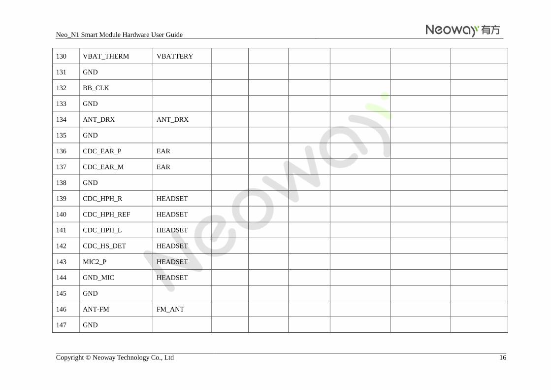
130 VBAT_THERM VBATTERY
131 GND
132 BB_CLK
133 GND
134 ANT_DRX ANT_DRX
135 GND
136 CDC_EAR_P EAR
137 CDC_EAR_M EAR
138 GND
139 CDC_HPH_R HEADSET
140 CDC_HPH_REF HEADSET
141 CDC_HPH_L HEADSET
142 CDC_HS_DET HEADSET
143 MIC2_P HEADSET
144 GND_MIC HEADSET
145 GND
146 ANT-FM FM_ANT
147 GND

Neo_N1 Smart Module Hardware User Guide
Copyright © Neoway Technology Co., Ltd 17
148 MIC1_N PRIMARY MIC
149 MIC1_P PRIMARY MIC
150 GND
151 SPKR_DRV_M SPKR
152 SPKR_DRV_P SPKR
2.3 GPIO Reference Level
Level Status I/O Min MAX Unit
GPIO 1.8 V digital I/O (VDD =1.8V)
VIH High level I 0.65*VDD — V
VIL Low level I 0.35 * VDD_ V
VOH High level O VDD- 0.45 V
VOL Low level O 0.45 V

Neo_N1 Smart Module Hardware User Guide
Copyright © Neoway Technology Co., Ltd 18
2.4 PCB Foot Print
LCC packaging is adopted to package the pins of the N1 module. Figure 2-2 shows the recommended
PCB foot print. (Unit: mm)
Figure 2-2 PCC foot print recommended for N1
The thickness of the solder paste and PCB flatness are keys to the acceptance rate during the production.
It is recommended that you prepare 0.15 mm to 0.20 mmstencils for mounting N1 and the stencil
apertures should be smaller than the pads of the module. Please use carriers during SMT or reflow
soldering process in case of improper soldering due to PCB bow and twist if your PCB boards are too thin
or long.

Neo_N1 Smart Module Hardware User Guide
Copyright © Neoway Technology Co., Ltd 19
3 Power Supply Interfaces
3.1 Power Supply Pins
VBAT is the power supply of the module. Its input voltage ranges from 3.5 V to 4.2V and the preferable
value is 3.9V. In addition to digital baseband and analogue baseband, it supplies power for RF power
amplifier. The performance of the VBAT power supply is a critical path to module's performance and
stability. The peak input current at the VBAT pin can be up to 2 A when the signal is weak and the module
works at the maximum transmitting power. The voltage will encounter a drop in such a situation. The
module might restart if the voltage drops lower than 3.5 V.
The pins 2 and 3 are the input of the power supply. Ensure that VBAT is above 3.5 V when the current
burst to 3A. Otherwise, the module will power off. Ensure that the trace between the VBAT pin and the
power supply on PCB board is wide enough to ease the voltage drop in a burst.
Figure 3-1 Current peaks and voltage drops
Keep above 3.5 V
3.5 V
0 ms 3.7 ms 7.4 ms 10.7 ms T
3 A
Voltage
Input
current
3.9 V
Figure 3-2 shows the reference design of the VRTC power supply.

Neo_N1 Smart Module Hardware User Guide
Copyright © Neoway Technology Co., Ltd 20
Figure 3-2 Capacitors used for the power supply
N1
Close to the module
D1 C1 C2 C3 C4 C5
VBATTest point
I_max
Power supply
In Figure 3-2, you can use TVS at D1 to enhance the performance of the module during a burst.
SMF5.0AG (Vrwm=5V&Pppm=200W) is recommended. A large bypass tantalum capacitor (220 μF or
100 μF) or aluminum capacitor (470 μF or 1000 μF) is expected at C1 to reduce voltage drops during
bursts together with C2 (10 μF ceramics capacitor). It is recommended that you add 0.1 uF, 100 pF, and 33
pF filter capacitors to enhance the stability of the power supply.
The module might fail to reset or power on/off in remote or unattended applications, or in an
environment with great electromagnetic interference (EMI). A controllable power supply is preferable
if used in harsh conditions. You can use the EN pin on the LDO or DC/DC chipset to control the switch of
the power supply as shown in Figure 3-3 if a 5V power supply is used.
MIC29302WU in Figure 3-3 is an LDO and outputs 3 A current to ensure the performance of the module.
Figure 3-3 Reference design of power supply control
VCC_IN_5V
VBAT
100 uF
TAN
0.1 uF
TVS
5V10 uF470uF
TAN
10K
4.75K
VOUT
MIC29302WU
EN
VIN ADJ
0.1 uF 100pF 33pF
PWR_EN
The alternative way is to use an enhancement mode p-MOSFET to control the module's power, as shown
in Figure 3-4. When the external MCU detects the exceptions such as no response from the module or the

Neo_N1 Smart Module Hardware User Guide
Copyright © Neoway Technology Co., Ltd 21
disconnection of GPRS, power off/on can rectify the module exceptions. In Figure 3-4, the module is
powered on when PWR_EN is set to high level.
Figure 3-4 Reference design of power supply controlled by p-MOSFET
VCC_IN_3.9V VBAT
10K
100K33 pF10 uF
2K
10K
0.1 uF
Q1
R4C1 C2C4 C5 C7
R1
R2
10 uF 0.1 uF
R3
Q2
TVS
5V
470 uF
C3 C6
100pF
S
G
D
PWR_EN
Q2 is added to eliminate the need for a high enough voltage level of the host GPIO. In case that the GPIO
can output a high voltage greater than VCCIN - |VGS(th)|, where VGS(th) is the Gate Threshold Voltage,
Q2 is not needed.
Reference components:
Q1 can be IRML6401 or low Rds(on) pMOSFET which has higher withstand voltage and drain
current.
Q2: a common NPN tripolar transistor, e.g. MMBT3904; or a digital NPN tripolar transistor, e.g.
DTC123. If digital tripolar transistor is used, delete R1 and R2.
C3: 470 μF tantalum capacitor rated at 6.3V; or 1000 μF aluminum capacitor. If lithium battery is
used to supply power, C3 can be 220 μF tantalum capacitor.
Power Supply Protection
Add TVS diodes (VRWM=5 V) on the VBAT power supply, especially in automobile applications. For
some stable power supplies, zener diodes can decrease the power supply overshoot. SMF5.0AG from
ONSEMI is an option.

Neo_N1 Smart Module Hardware User Guide
Copyright © Neoway Technology Co., Ltd 22
PCB Trace
The trace width of primary loop lines for VBAT on PCB must be able to support the safe transmission of 2
A current and ensure no obvious loop voltage decrease. Therefore, the trace width of VBAT loop line is
required at 2 mm and the ground level should be as complete as possible.
Separation
The module works in burst mode that generates voltage drops on power supply. Furthermore, this results
in a 217Hz TDD noise through power (One of the way generating noise. Another way is through RF
radiation). Analog parts, especially the audio circuits, are subjected to this noise, known as a "buzz noise"
in GSM systems. To prevent other parts from being affected, it is better to use separated power supplies.
The module shall be supplied by an independent power, like a DC/DC or LDO. See Figure 3-5.
DC/DC or LDO should output rated peak current larger than 2 A.
The inductor used in Reference Design (b), should be a power inductor and have a very low resistance.
The value of 10 μH, with average current ability greater than 1.2A and low DC resistance, is
recommended.
Figure 3-5 Reference designs of separated power supply
Other circuitDC-DC/LDO
N1DC-DC/LDO
Power
Input
Other circuitDC-DC/LDO
N1
Power
Input 10 uF
Reference design (a) Reference design (b)
Never use a diode to make the drop voltage between a higher input and module power. Otherwise,
Neoway will not provide warranty for product issues caused by this. In this situation, the diode will
obviously decrease the module performances, or result in unexpected restarts, due to the forward voltage
of diode will vary greatly in different temperature and current.
EMC Considerations for Power Supply
Place transient overvoltage protection components like TVS diode on power supply, to absorb the power
surges. SMAJ5.0A/C could be a choice.

Neo_N1 Smart Module Hardware User Guide
Copyright © Neoway Technology Co., Ltd 23
3.2 Power-On
After powering on the VBAT pin, you can use PWR_N to start the module by inputting low-level pulse
for 3 seconds. This pin is pulled up internally. Its typical high-level voltage is 1.8 V. Do not leave this pin
disconnected. The following circuit is recommended to control PWR_N.
Figure 3-6 Push switch controlling
PWR_NR1S1
Figure 3-7 MCU controlling
USER_ONPWR_N
R3
R2
If the module is powered on but the power-on sequence has not been completed, the states of each pin are
uncertain. The power-on sequence of the module is shown as Figure 3-8.
Figure 3-8 N1power-on sequence
VBAT
OTHERS
3s
30s
RESIN_N
Not defined

Neo_N1 Smart Module Hardware User Guide
Copyright © Neoway Technology Co., Ltd 24
3.3 Hard Reset
The RESIN_N pin is used to reset the module. It triggers module reset when you input low-level pulse for
3 seconds. This pin is pulled up internally. Its typical high-level voltage is 1.8 V. Leave this pin
disconnected if you do not use it. If you use a 2.8V/3.3V IO system, it is recommended that you add a
triode to separate it. Refer to the following design.
Figure 3-9 Reset controlled by button
R1S1
RESIN_N
Figure 3-10 Reset circuit with triode separating
2V8/3V3R 3
R 2
0V
VDD_ EXT
Q 1 RESIN_N
In a circuit shown in Figure 3-10, VDD_EXT=2.8V/3.3V/3.0V, R2=4.7K, R3=47K. Figure 3-11 shows
the reset sequence.
Figure 3-11 N1reset sequence
VBAT
OTHERS
3s
Not defined
RESIN_N
40s

Neo_N1 Smart Module Hardware User Guide
Copyright © Neoway Technology Co., Ltd 25
3.4 Hard Power-off
The PWR_N input pin can be used to hard power off the module. Low-level pulse input for 13 seconds
can trigger the power-off of the module. This pin is pulled up internally. Its typical high-level voltage is
1.8 V. Leave this pin disconnected if you do not use it. If you use a 2.8V/3.3V IO system, it is
recommended that you add a triode to separate it. Refer to 3.3Hard Reset. Figure 3-12 shows the hard
power-off sequence.
Figure 3-12 N1power-off sequence
VBAT
OTHERS
13s
PWR_N
Not defined
3.5 VRTC Power Supply
Pin Signal I/O Function Remarks
125 VRTC I/O RTC power supply 2V to 3.25V, typical value 3V
VRTC is the pin that supplies power for the RTC of the module. A 22 μF capacitor is connected to VRTC
inside the module to keep the system clock working when you replace the power supply (battery) of the
module. The module will update the RTC clock after it is powered on and connected to the network.
Figure 3-13 shows the internal design of the VRTC pin.

Neo_N1 Smart Module Hardware User Guide
Copyright © Neoway Technology Co., Ltd 26
Figure 3-13 VRTC design in the module
N1
RTC
Circuit+
22µF
Backup
battery
3.6 Battery Management
Our N1module supports battery charging. For information about how to select proper battery, refer to GB
/T18287-2000 Chinese National Standard for Lithium Ion batteries for mobile phones. Available voltages
range between 3.5V to 4.2V. It is recommended that you connect ESD and capacitors to VBAT and
VBAT_THERM in parallel in case that abnormal electrical signal might damage the module.
PDA, mobile POS and other mobile devices all use battery as power supply. For different batteries, you
need to modify the charging/discharging curve in the software. N1provides two pins for battery.
Pin Signal I/O Function Remarks
2, 3 VBAT Power supply input 3.5V~4.2V
130 VBAT_THERM Battery temperature check
Ensure that the VBAT_THERM pin is connected. Otherwise, the battery might fail to charge or the
remaining power is displayed incorrectly. Figure 3-14 shows the connection of the battery pins, among
which C1 is 47uF, C2 is 100pF, R1 is 13KΩ, R2 is 2.1KΩ, recommended model for R_TH is
SDNT1005X103F3380FTF (10KΩ, precision of 1%), and the constant B is 3380.

Neo_N1 Smart Module Hardware User Guide
Copyright © Neoway Technology Co., Ltd 27
Figure 3-14 Battery connections
N1
VREF_BAT_THM
VBAT_THERM
PMIC
VBAT
R1
R2
R_T
H
GND
Battery
Module
C1 C2TVS

Neo_N1 Smart Module Hardware User Guide
Copyright © Neoway Technology Co., Ltd 28
4 Video I/O Interfaces
N1video I/O interfaces comply with Mobile Industry Processor Interface (MIPI) standard to transmit
high-speed digital signals. This standard is widely supported by main device manufacturers. So it is easy
to get video devices that support this standard.
4.1 LCD Interfaces
LCD interfaces are the video output interfaces of the N1module, developed based on the MIPI_DSI
standard. They support four groups of high-speed differential data transmission, each of which can
achieve a rate of at most 1.5 Gbps. You can configure different quantity of MIPI_DSI as required.
4.1.1 WVGA
The following sections will describe the hardware configuration of WVGA display that we have
commissioned.
The resolution size of WVGA display is 800 x 480, which requires two groups of MIPI_DSI. LCD design
is generally to connect FPC to the connector. Table 4-1lists the LCD pins.
WVGA LCD pin description
Pin Signal I/O Function Remarks
37 LCD_DIF DI ID
38 LCD_RST_N DO
43 MIPI_DSI0_CLK_M DO MIPI
44 MIPI_DSI0_CLK_P DO MIPI
41 MIPI_DSI0_LANE1_P DO MIPI
42 MIPI_DSI0_LANE1_M DO MIPI
45 MIPI_DSI0_LANE2_P DO MIPI
46 MIPI_DSI0_LANE2_M DO MIPI
39 LCD_TE DO
127 VREG_L17_2P85V AO AO Max: 350mA
126 VREG_L6_1P8V AO AO Max: 120mA
/ LED_K AI Anode of backlight boost converter
/ LED_A AO Cathode of backlight boost converter
/ VEXT_2P85V AO LDO output

Neo_N1 Smart Module Hardware User Guide
Copyright © Neoway Technology Co., Ltd 29
35 TS_RST_N DO Reset touchscreen
120 TS_I2C_SCL DO I2C clock
119 TS_I2C_SDA DIO I2C data
34 TS_INT_N DI Touchscreen interrupt
Ensurethat thetrace is shorter than 280 mm because MIPI is high-speed signal.
Ensure ±10% trace precision to achieve a differential impedance of 100 Ω for each differential pair
of traces.
In your design, add common mode chokes to the MIPI circuit to reduce the electromagnetic interference.
Figure 4-1 shows the reference circuits with common mode choked. Please refer to 4.4Design Cautions.
Figure 4-1 Reference MIPI circuits with common mode chokes
MIPI_DSI0_LANE1_M
MIPI_DSI0_LANE1_P
MIPI_DSI0_D1_M_LCD
MIPI_DSI0_D1_P_LCD
FL1
MIPI_DSI0_CLK_M
MIPI_DSI0_CLK_P
MIPI_DSI0_CLK_M_LCD
MIPI_DSI0_CLK_P_LCD
FL1
MIPI_DSI0_LANE2_M
MIPI_DSI0_LANE2_P
MIPI_DSI0_D2_M_LCD
MIPI_DSI0_D2_P_LCD
FL1
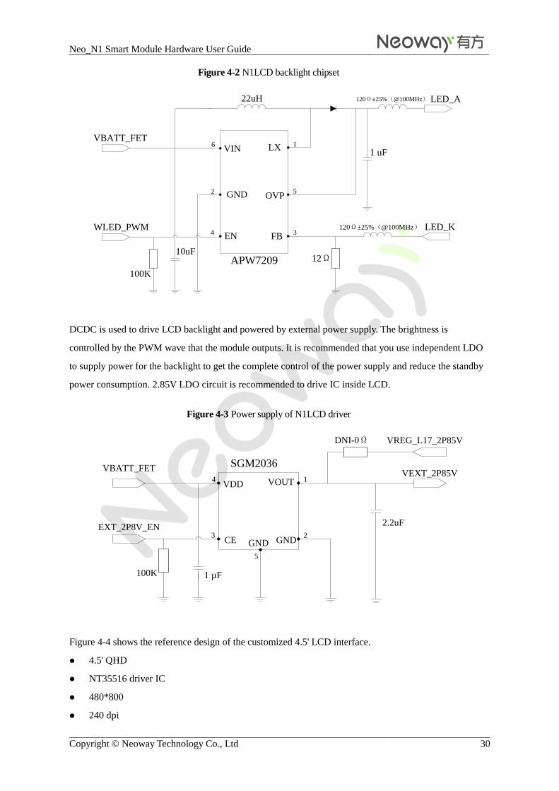
Figure 4-2 shows the backlight driver circuit.
Neo_N1 Smart Module Hardware User Guide
Copyright © Neoway Technology Co., Ltd 30
Figure 4-2 N1LCD backlight chipset
VBATT_FET
10uF
LX1 uF
OVPGND
VIN
APW7209
EN
1
52
6
FBWLED_PWM
100K
22uH
12Ω
120Ω±25%(@100MHz)
120Ω±25%(@100MHz) LED_K4 3
LED_A
DCDC is used to drive LCD backlight and powered by external power supply. The brightness is
controlled by the PWM wave that the module outputs. It is recommended that you use independent LDO
to supply power for the backlight to get the complete control of the power supply and reduce the standby
power consumption. 2.85V LDO circuit is recommended to drive IC inside LCD.
Figure 4-3 Power supply of N1LCD driver
EXT_2P8V_EN
1 µF
VOUT
2.2uF
GNDCE
VDD
SGM2036VBATT_FET
GND
100K
VEXT_2P85V1
2
5
3
4
DNI-0Ω VREG_L17_2P85V
Figure 4-4 shows the reference design of the customized 4.5' LCD interface.
4.5' QHD
NT35516 driver IC
480*800
240 dpi

Neo_N1 Smart Module Hardware User Guide
Copyright © Neoway Technology Co., Ltd 31
Capacitive multi-touch
See Figure 4-4.
Figure 4-4 Reference design of LCD interface
LCD connector
2524
2322
2120
1918
1716
1514
13
9
1112
10
8
6
4
2
7
5
3
1
27
26
220Ω±25%(@100MHz)
LCD_DIF
LCD_RST_N
VREG_L19_2P85
LED_A
TS_I2C_SCL
0.1uF 1uF
0.1uF1uF 0.1uF
V
AV
L-5
.5V
-10
0P
F
1uF
1 2 3
4 5
FV1
V
LCD_ID
MIPI_DSIO_D2_M_LCD
MIPI_DSIO_CLK_M_LCD
MIPI_DSIO_D1_M_LCD
LCD_TE
VREG_L14_1P8V
LED_K
TS_RST_N
TS_I2C_SDA
MIPI_DSI0_D2_P_LCD
MIPI_DSI0_CLK_M_LCD
MIPI_DSI0_D1_P_LCD
VEXT_2P85V
TS_INT_N
AV
L-5
.5V
-10
0P
F
4.1.2 720P
If you select 720P touch panel, 4groups of MIPI_DSIare required. For the basic design, see WVGA. The
following table lists the 720P LCD pins.
720P LCD Pin description
Pin Signal I/O Function Remarks
37 LCD_DIF DI ID
38 LCD_RST_N DO
43 MIPI_DSI0_CLK_M DO MIPI
44 MIPI_DSI0_CLK_P DO MIPI
49 MIPI_DSI0_LANE0_M DO MIPI
50 MIPI_DSI0_LANE0_P DO MIPI
41 MIPI_DSI0_LANE1_P DO MIPI

Neo_N1 Smart Module Hardware User Guide
Copyright © Neoway Technology Co., Ltd 32
42 MIPI_DSI0_LANE1_M DO MIPI
45 MIPI_DSI0_LANE2_P DO MIPI
46 MIPI_DSI0_LANE2_M DO MIPI
47 MIPI_DSI0_LANE3_M DO MIPI
48 MIPI_DSI0_LANE3_P DO MIPI
39 LCD_TE DO
127 VREG_L17_2P85V AO AO Max: 350mA
126 VREG_L6_1P8V AO AO Max: 120mA
/ LED_K AI Anode of backlight boost converter
/ LED_A AO Cathode of backlight boost converter
/ VEXT_2P85V AO LDO output
35 TS_RST_N DO Reset touchscreen
120 TS_I2C_SCL DO I2C clock
119 TS_I2C_SDA DIO I2C data
34 TS_INT_N DI Touchscreen interrupt
4.2 TP Interfaces
TP and LCD cannot be the FPC interface. Table 4-3 lists the TP pins. Figure 4-5 shows the reference
design of customized 4.5' TP interfaces, in which ESD protection array is added. The recommended ESD
models include NZQA5V6AXV5T1G, CESDLC3V0L4, PESD3V3V4UW, etc.
TP pins
Pin Signal I/O Function Remarks
/ CAM_1P8V AO Power output
/ VEXT_2P85V AO LDO output
35 TS_RST_N DO Reset TP
119 TS_I2C_SDA DIO I2C data
120 TS_I2C_SCL DO I2C clock
34 TS_INT_N DI TP interrupt

Neo_N1 Smart Module Hardware User Guide
Copyright © Neoway Technology Co., Ltd 33
Figure 4-5 Reference design of TP interface
TP connector
8
6
4
2
7
5
3
1
9 10
1uF
V
AV
L-5
.5V
-10
0P
F
V
AV
L-5
.5V
-10
0P
F
1 2 3
FV1
1uF0.1uF 0.1uF
47KΩ DNI-47KΩ
4 5
VEXT_2P85V
CAM_1P8V
CAM_1P8V
TS_RST_N
TS_I2C_SCL
TS_I2C_SDA
TS_INT_N
4.3 Camera Interfaces
The video input interfaces of the module is developed based on the MIPI_CSI standard, and support two
cameras, among which the pixel can be at most 8MP. The quality of video and photo is dependent on the
camera sensor, the camera specifications, and other factors. You can select cameras compliant with your
application scenarios based on the list of camera specifications that we have commissioned.
Neoway commissioned the following camera models:
Main camera: OV5670 (5MP), optional, OV5648 (5MP)
Sub camera: OV2680(2MP)
4.3.1 Main Camera
The main camera transmits data and is controlled through FPC and connector. It uses two groups of
MIPI_CSI differential data interfaces, and support at most 8MP. Table 4-4 lists pins of the main camera.

Neo_N1 Smart Module Hardware User Guide
Copyright © Neoway Technology Co., Ltd 34
Main camera pins
Pin Signal I/O Function Remarks
52 MIPI_CSI0_LANE0_P MIPI
53 MIPI_CSI0_LANE0_M MIPI
54 MIPI_CSI0_CLK_P MIPI
55 MIPI_CSI0_CLK_M MIPI
56 MIPI_CSI0_LANE1_P MIPI
57 MIPI_CSI0_LANE1_M MIPI
69 REAR_CAM_RST_N Reset
64 REAR_CAM_MCLK Clock
74 CAM _I2C_SDA I2C data
73 CAM _I2C_SCL I2C clock
/ VEXT_2P85 LDO output
/ VEXT_CAM_1P2V LDO output
/ VEXT_CAM_1P8V LDO output
LDO supplies power for VEXT_2P85, VEXT_CAM_1P2V, and VEXT_CAM_1P8V. The recommended
LDO models are respectively:
RP100K281B5-TR, RP100K281D5-TR, RP100K281D-TR, XC6221A282GR, XC6221B282GR;
RP100K121B-TR, TK68112AMFG0L-C, XC6221A122GR, XC6221B122GR;
RP100K181D-TR, TK64118AMFGOL-C, XC6221A182GR, RP100K181B-TR, XC6221B182GR.
Figure 4-6 shows the reference design of the 5MP main camera.

Neo_N1 Smart Module Hardware User Guide
Copyright © Neoway Technology Co., Ltd 35
Figure 4-6 Reference design of the main camera interface
Main camera
connector
12
34
56
78
910
1112
13
17
1514
16
18
20
22
24
19
21
23
25
27
26
0Ω
VEXT_2P85V
CAM0_RST_N/BLSP3_SPI_CS_N
MIPI_CSI0_CLK_M
CAM_I2C_SCL
MIPI_CSI0_LANE1_M
1uF 1uF0.1uF2.2uF
1uF
CAM_I2C_SDACAM0_MCLK
DGND
DGND
MIPI_CSI0_LANE1_P
MIPI_CSI0_CLK_PMIPI_CSI0_LANE0_M
MIPI_CSI0_LANE0_P
PWDN_VCM
VREG_L6_1P8EXT_1V2_DVDD
VEXT_2V85_AVDD
4.3.2 Sub-Camera
Sub-camera uses one group of MIPI_CSI differential signal, and supports 2MP cameras. Table 4-5 lists
sub-camera pins.
Sub-camera pins
Pin Signal I/O Function Remarks
59 MIPI_CSI1_LANE0_M DO MIPI
60 MIPI_CSI1_LANE0_P DO MIPI
61 MIPI_CSI1_CLK_P DO MIPI
62 MIPI_CSI1_CLK_M DO MIPI
72 CAM1_RST_N DO RESET
73 CAM _I2C_SCL O I2C clock
74 CAM _I2C_SDA IO I2C data
65 CAM1_MCLK O Clock
/ VEXT_2P85V O LDO output
/ VEXT_CAM_1P8V O LDO output
VEXT_2P85V and VEXT_CAM_1P8V are powered by LDO. For information about how to select the
proper model, see 4.3.1Main Camera.

Neo_N1 Smart Module Hardware User Guide
Copyright © Neoway Technology Co., Ltd 36
Figure 4-7 shows the reference design of 2MP camera.
Figure 4-7 Reference design of sub-camera interface
Sub camera connector
13
12
11
10
9
8
7
6
5
4
3
2
1
14
15
0.1
uF
2.2
uF
0.1
uF
1u
F
VEXT_2P85V
VREG_L6_1P8
CAM1_RST_N/BLSP4_SPI_CLK
CAM_I2C_SCL
CAM_I2C_SDA
CAM1_MCLK1
MIPI_CSI1_LANE0_P
MIPI_CSI1_LANE0_M
MIPI_CSI1_CLK_M
MIPI_CSI1_CLK_P
CAM1_PWDN
EXT_1V2_DVDD
2.2
uF
0.1
uF
4.3.3 Design Cautions
Please note the scanning direction of the camera, the aiming direction, and angle of the camera lens, the
scanning method of the LCD when it reads data.
LCD is generally designed in two ways: vertical scan and horizontal scan. LCD is generally designed in
two ways: vertical scan and horizontal scan.
Figure 4-8 Scan direction of 3264*2448 LCD
Generally, our customized LCD supports horizontal scan. Figure 4-9 shows the reference design of our
customized camera.

Neo_N1 Smart Module Hardware User Guide
Copyright © Neoway Technology Co., Ltd 37
Figure 4-9 Reference design of customized camera
Images from the camera to the LCD can be adjusted in only four ways:
Figure 4-10 Adjustment of camera sensor
Images can be displayed correctly only when the camera sensor and the LCD scan in the same direction.
If the camera sensor and LCD scan in different directions, the image will be mirrored.

Neo_N1 Smart Module Hardware User Guide
Copyright © Neoway Technology Co., Ltd 38
4.3.4 Camera Power Supply
LDO supply power for cameras separately. For the recommended models, see 4.3.1Main Camera. The
1.8V LDO circuit is used for the reference IC level inside the camera. Figure 4-11 shows the reference
circuit.
Figure 4-11 Reference design of the main camera power supply
EXT_2P8V_EN
1 uF
VOUT
2.2uF
GNDCE
VDD
SGM2036VBATT_FET
GND
100K
VEXT_2P85V1
2
5
3
4
DNI-0Ω VREG_L17_2P85V
1.2V level input is required for main camera. Figure 4-12 shows the reference design.
Figure 4-12 Reference design of the main camera power supply
VDD4
VOUT1
CE3
GND2
GND
5
VBATT_FET
EXT_1V2_EN2.2 uF
EXT_1V2
1 uFDNI-100K
SGM2360
N1has specific enable control pins for each LDO circuit. The voltage varies with the cameras. For details,
see the reference design.

Neo_N1 Smart Module Hardware User Guide
Copyright © Neoway Technology Co., Ltd 39
4.4 Design Cautions
Please note the definition of the video interfaces and ensure the correct connection between the connector
and components.
The MIPI transmission rate can reach 1.5 Gbps. Use 50Ω design rules to achieve a differential impedance
of 100 Ω for the differential pair of traces, which must be routed on the inner layer to isolate from other
signal traces. Keep length matching for the MIPI traces of one video component. Reserve 1.5 times of
trace width between MIPI traces. It is recommended that you lay all MIPI traces on the same layer.

Neo_N1 Smart Module Hardware User Guide
Copyright © Neoway Technology Co., Ltd 40
5 Audio Interface
N1provides a few groups of audio input/output interfaces to meet your requirements in different
applications.
5.1 Audio Input
Table 5-1 lists the two groups of audio input pins.
Audio input pins
Pin Signal I/O Function Remarks
148 MIC1_N AI Negative electrode of MIC1 output Main MIC
149 MIC1_P AI Positive electrode of MIC1 output Main MIC
143 MIC2_P AI Positive electrode of MIC2 output Sun-MIC
Figure 5-1 shows the differential connection of the peripheral. A bias circuit is embedded for the audio
input pins. TVS in Figure 5-1 can be replaced by AVLC5S02100 and SDV1005E5R5C800NPTF.
Figure 5-1 Reference design of MIC connection
N1
33 pF
MIC
33 pF
33 pF
MICN
MICP
TVS TVS
1800Ω±25%(@100MHz)
1800Ω±25%(@100MHz)
5.2 Audio Output
N1provides a few groups of audio output interfaces, including speaker, receiver, and headphone. Table 5-2
lists the audio output pins.

Neo_N1 Smart Module Hardware User Guide
Copyright © Neoway Technology Co., Ltd 41
Audio output pins
Pin Signal I/O Function Remarks
136 CDC_EAR_P AO Positive electrode of receiver output
137 CDC_EAR_M AO Negative electrode of receiver output
151 SPKR_DRV_M AO Negative electrode of speaker output
152 SPKR_DRV_P AO Positive electrode of speaker output
The speaker pins support Class D amplifier and differential output. The typical speaker output power is
1.4W/0.95W@8Ω when the battery supplier 5V/4.2V, 2W/1W@4Ω when the battery supplier 5V/3.6V.
The speaker can provide overburst protection and noise rejection.
Figure 5-2 shows the reference design of the audio output pins.
Figure 5-2 Reference design of EAR/SPK connections
33 pF
33 pF
EAR/SPK-
EAR/SPK+
33 pF
N1
EAR/SPK
1800Ω±25%(@100MHz)
1800Ω±25%(@100MHz)
TVSTVS
5.3 Headphone Interfaces
The module provides fixed pins to achieve the headphone function. N1supports class AB headphone
amplifier and three headphone control buttons. Table 5-3 lists the headphone pins.
Headphone pins
Pin Signal I/O Function Remarks
141 CDC_HPH_L AO Left sound channel of the earphone output
140 CDC_HPH_REF Headphone output level
139 CDC_HPH_R AO Right sound channel of the earphone output
143 MIC2_P AI Audio input of MIC2, used for single-end
headphone input

Neo_N1 Smart Module Hardware User Guide
Copyright © Neoway Technology Co., Ltd 42
142 CDC_HS_DET DI Headphone detection
Figure 5-3 shows the reference design of the headphone circuit.
Figure 5-3 Reference design of headphone without FM
34
1
52 V V
10K
1000Ω±25%(@100MHz)
1000Ω±25%(@100MHz)
1000Ω±25%(@100MHz)
1000Ω±25%(@100MHz)
1000Ω
±25%
(@100M
Hz
)
1000Ω±25%(@100MHz)
V
10K
33pF
470pF
AV
L-5
.5V
-100P
F
AV
L-5
.5V
-100P
F
AV
L-5
.5V
-100P
F
470pF
DNI-33pF
PE
SD
5V
0S
1B
L
Headphone connector
MIC2_P
CDC_HPH_R
CDC_HPH_L
CDC_HS_DET
CDC_HPH_REF
Figure 5-4 shows the circuits of headphone out of position and in position.

Neo_N1 Smart Module Hardware User Guide
Copyright © Neoway Technology Co., Ltd 43
Figure 5-4 Headphone interface
Please note if headphone you select is CTIA or OMTP. The connections of ①and ② are reverse for the
two type of headphones. The CDC_HS_DET pin (⑤in the above figure) is left disconnected (pulled up
internally) if the headphone is not plugged. After the headphone is plugged, this pin is connected to GND
through the left channel (8/16/32 Ω) loudspeaker of the headphone.
5.4 Audio Design Cautions
The audio signal traces should be wide enough on the PCB to bear large current when the module output
audios at the highest volume. The traces should be isolated from digital signals and clock as well as other
analog signal traces.No signal trace crossing is allowed.Reserve enough grounding holes and ground
protection.
Do not connect the audio output pins to GND.

Neo_N1 Smart Module Hardware User Guide
Copyright © Neoway Technology Co., Ltd 44
6 Peripheral Interfaces
6.1 USB Interface
You can download programs for N1and establish data connections through the USB interface. If the
module is used only as USB Device, the recommended USB circuit is shown in Figure 6-1.
Figure 6-1 USB circuit(without OTG)
Micro USB
VBUS_USB_IN
22PF E
SD
9X
5V
U
ES
D9
X5
VU
PE
SD
5V
0S
1B
L
DNI-18PF
0Ω
0Ω
USB_DM
USB_DP
USB_HS_ID
1UF
Parallel a 1μF and 22pF filter capacitors to the VBUS_USB_IN pin as close to the pin as possible. TVS
components are required for the VBUS power line. The junction capacitance of the TVS protection diodes
for USB_DP and USB_DM should be lower than 12pF as possible. USB data lines adopt differential trace
design, in which the differential impedance is limited to 90 Ω characteristics impedance. Isolate the traces
from other signal traces.

Neo_N1 Smart Module Hardware User Guide
Copyright © Neoway Technology Co., Ltd 45
Figure 6-2 USB circuit (with OTG)
USB_DMUSB_DM
USB_DPUSB_DP
GNDGNDUSB_HS_IDUSB_HS_ID
0Ω0Ω
0Ω0Ω
ES
D9
X5
VU
ES
D9
X5
VU
GPIOGPIO
VBATVBAT VBATVBAT
VINVINAW3610AW3610
SWSW1UH1UH
ES
D9
X5
VU
ES
D9
X5
VU
VBUS_USB_INVBUS_USB_IN
MICRO USBMICRO USB
USB_HS_IDUSB_HS_IDUSB_DPUSB_DP
USB_DMUSB_DM
VBUS_USB_INVBUS_USB_IN PE
SD
5V
0S
1B
LP
ES
D5
V0
S1
BL
ENEN
VOUTVOUT
VOUTVOUTGNDGND
AM809AM809
22PF22PF 1UF1UF
N1supports USB OTG. You can refer to the above circuit if you need the USB OTG function. You can
select the DC-DC model based on your requirements.
6.2 UIM Card Interface
N1supports 1.8V/2.85V SIM cards. N1allows dual SIM cards. VREG_UIM is the power supply pin of the
SIM card and its maximum load is 30 mA. The UIM_DATA pin is not pulled up internally, so you need to
reserve external pull-up resistor in your design. UIM_CLK is the clock signal pin, supporting 3.25 GHz of
clock frequency. Figure 6-3 shows the reference design of the SIM card interface.
Figure 6-3 Reference design of SIM card interface
1 uF
UIM_DATA
UIM_CLK
UIM_RST
VREG_UIM
N1
CLK
RST
VCC
VPP
GND
SIM card
DATA
GNDSIM-DetUIM_DETECT
10K
ESD protectors, such as ESD diodes or ESD varistors (with a junction capacitance of less than 33 pF), are
recommended on the SIM signals, especially in automotive electronics or other applications with badly

Neo_N1 Smart Module Hardware User Guide
Copyright © Neoway Technology Co., Ltd 46
ESD. Replace the ESD diodes with 27 pF to 33 pF capacitors connecting to GND in common applications.
The ESD diodes or small capacitors should be close to SIM card.
N1supports SIM card detection. SIM1_DETECT/ SIM2_DETECT are 1.8V interrupt pins. Low level
means SIM card detected while high level mean no SIM card detected.
The antenna should be installed far away from the SIM card and SIM card traces, especially to the
build-in antenna.
The SIM traces on the PCB should be as short as possible and shielded with GND copper.
The ESD protection diodes or small capacitors should be closed to SIM card on the PCB.
6.3 SDIO
N1supports SD/MMC cards of 4-bit mode, or devices based on the SDIO protocol and the latest SDIO 3.0
protocol.
6.3.1 SD Card
Figure 6-4 shows the reference design of the camera power supply.
Figure 6-4 Reference design of TF card interface
DAT2
CD/DAT3
CMD
VDD
TF connector
CLK
VSS
DAT0
DAT1
GND
GND
GND
GND
1 2 3
4 5
1 2 3
4 5
FV1 FV2
0.1
uF
4.7
uF
VREG_SDC_PWR
SDC2_DATA2
SDC2_DATA3
SDC2_CMD
SCD2_CLK
SCD2_DATA0SCD2_DATA1
Table 6-1 lists TF card pins.

Neo_N1 Smart Module Hardware User Guide
Copyright © Neoway Technology Co., Ltd 47
TF card pins
Pin Signal I/O Function Remarks
26 VREG_SDC_PWR PWR
SDIO driver power supply, supporting dual
voltage of 1.8V and 2.95V, maximum current
500 mA
VDD
25 SDC2_CMD O Command line, impedance line recommended CMD
27 SDC2_CLK O High-speed digital clock CLK
28 SDC2_DATA0 IO High-speed data line DATA0
29 SDC2_DATA1 IO High-speed data line DATA1
23 SDC2_DATA2 IO High-speed data line DATA2
24 SDC2_DATA3 IO High-speed data line DATA3
30 SD_CARD_DET_N I SD card detection, low-level interrupt /
VREG_SDC_PWR is the power supply pin of the SD card. It supports a maximum current of 500mA and
dual-voltage of 1.8V/2.95V. The recommended trace width is 0.5 mm. Parallel 0.1 μF and 4.7 μF
capacitors to the SD card.
CMD, CLK, DATA0, DATA1, DATA2 and DATA3 are high-speed signal lines. Limit their characteristics
impedance to 50Ω and do not let them cross any other traces. Keep length matching for CMD, DATA0,
DATA1, DATA2 and DATA3 traces. CLK trace should be ground separately.
6.3.2 SD Peripheral Interface
SDIO interface can connect other peripherals. Refer to the SD card connection design, and connect the
module pin to the peripheral pin directly. PCB layout is similar to the SD card design.
6.4 GPIO
N1supports multiple standards including UART, I2C, and SPI. You can configure the GPIO to meet your
requirements for connecting to different devices. For the open multi-function GPIO interface, please
inquiry our technical support engineers.
GPIO pins
Pin Signal General Function Alternate Function 1
Alternate
Function 2 GPIO
32 GPIO_15 GPIO_15 BLSP4_SPI_CLK GP_CLK_2B 15
33 GPIO_14 GPIO_14 BLSP4_SPI_MISO GP_CLK_1B 14
34 TS_INT_N TS_INT_N BLSP4_SPI_MISO GP_CLK_3B 13

Neo_N1 Smart Module Hardware User Guide
Copyright © Neoway Technology Co., Ltd 48
35 TS_RST_N TS_RST_N BLSP4_SPI_MOSI GP_CLK_2B 12
77 SENSORS_I2C_SC
L
SENSORS_I2C_SC
L BLSP1_SPI_CLK
BLSP1_UART
_RFR_N 7
78 SENSORS_I2C_SD
A
SENSORS_I2C_SD
A BLSP1_SPI_CS_N
BLSP1_UART
_CTS_N 6
79 UART1_MSM_RX UART1_MSM_RX/ BLSP1_SPI_MISO BLSP1_UART
_RX 5
80 UART1_MSM_TX UART1_MSM_TX/ BLSP1_SPI_MOSI BLSP1_UART
_TX 4
90 GPIO_3 GPIO_3 MI2S_2_D1 3
91 GPIO_2 GPIO_2 MI2S_2_D0 2
92 GPIO_1 GPIO_1 MI2S_2_SCK 1
93 GPIO_0 GPIO_0 MI2S_2_WS 0
97 I2C_SCL I2C_SCL BLSP2_SPI_CLK BLSP2_I2C_S
CL 112
98 I2C_SDA I2C_SDA BLSP2_SPI_CS_N BLSP2_I2C_S
DA 111
99 UART2_MSM_RX UART2_MSM_RX BLSP2_SPI_MISO BLSP2_UART
_RX 21
100 UART2_MSM_TX UART2_MSM_TX BLSP2_SPI_MOSI BLSP2_UART
_TX 20
110 BLSP6_SPI_CLK BLSP6_SPI_CLK BLSP6_SPI_CLK 11
111 BLSP6_SPI_CS_N BLSP6_SPI_CS_N BLSP6_SPI_CS_N 10
112 BLSP6_SPI_MISO BLSP6_SPI_MISO BLSP6_SPI_MISO 9
113 BLSP6_SPI_MOSI BLSP6_SPI_MOSI BLSP6_SPI_MOSI 8
114 GPIO_16 GPIO_16 BLSP5_SPI_MOSI 16
118 GPIO_17 GPIO_17 BLSP5_SPI_MISO 17
119 TS_I2C_SDA TP BLSP5_SPI_CS_N 18
120 TS_I2C_SCL TP BLSP5_SPI_CLK 19
6.4.1 UART
N1provides two groups of UART interfaces, which support 4Mbps at most. The reference high level is
1.8V. Figure 6-5 shows the reference design of the UART interface.

Neo_N1 Smart Module Hardware User Guide
Copyright © Neoway Technology Co., Ltd 49
Figure 6-5 Reference design of the UART interface
N1
URXD
UTXD
Client
UTXD
URXD
If the UART is interfacing with a MCU that has 5 V logic levels, it is recommended that you add a level
shifting circuit outside of the module as shown in Figure 6-6.
Figure 6-6 Recommended circuit for the communication between 5V MCU and UART
Components:
R2: 2K-10K. The greater the UART baudrate is, the lower the R2 value is.
R3: 4.7K-10K The greater the UART baudrate is, the lower the R3 value is.
Q1: MMBT3904 or MMBT2222 High-speed transistor is better.
Logic level DTE 5V —> DCE 1.8V:
Figure 6-6 shows the circuit between MCU TXD and module RXD. The INPUT pin is connected to MCU
TXD and OUTPUT is connected to RXD of the module. VCC_IN supplies 5V and VCC_OUT supplies
1.8V.
The circuit between MCU RXD and module TXD can also adopt the connection in Figure 6-6. The
INPUT pin is connected to module TXD and OUTPUT is connected to MCU RXD. VCC_IN supplies
1.8V and VCC_OUT supplies 5V.
OUTPUT
VCC_IN VCC_OUT
4.7K 10KR2 R3
INPUT Q1

Neo_N1 Smart Module Hardware User Guide
Copyright © Neoway Technology Co., Ltd 50
6.4.2 I2C
N1provides one group of I2C interfaces, which support the host mode only. The I2C interfaces are
open-drain driven (pull-up resistor is mandatory for the external circuit). They support a maximum rate of
3.4 Mbps and their reference high level is 1.8V. Figure 6-7 shows the reference design of the I2C
interfaces.
Figure 6-7 Reference design of I2C
2.2K 2.2K
1.8V
I2C-SCL
I2C-SDA
I2C-SCL
I2C-SDA
6.4.3 SPI
N1provides a group of SPI interfaces, which support the host mode only. The maximum rate is 52MHz,
and the reference high level is 1.8V. Figure 6-8 shows the reference design of SPI interfaces.
Figure 6-8 Reference design of the SPI
SCLK
SS
MISON1
MOSI
GND
Master
SCLK
SS
MISO
MOSI
GND
Slave
TXS0104E or NLSX4373MUTAG is recommended if you need level shifter to shift the level of the
UART, IIC, SPI, etc. Do not connect interfaces of different level standards directly. Otherwise, the module
might be damaged.

Neo_N1 Smart Module Hardware User Guide
Copyright © Neoway Technology Co., Ltd 51
6.5 ADC
N1provides only ADC channel. ADC pin supports highest precision of 10-bit. Table 6-3 lists the ADC
pins.
ADC pin
Pin Signal I/O Function Remarks
129 ADC_IN AI ADC pin Reference voltage: 1.25V
130 VBAT_THERM AI Battery temperature check The battery cannot be charged till this
pin is connected.
6.6 Other Interfaces
N1also provides motor driver interface and key backlight driver interface to meet the requirements for
mobile device applications.
Motor is driven by specific circuit. Figure 6-9 shows the reference design of the motor circuit.
Figure 6-9 Reference design of motor circuit
Motor
interface
+
2.2pF
33pF
0Ω
0.1uF
0ΩVBATT_FET VIB_DRV_N
33pF
The diode loop can release the electricity on the motor to protect the component when the VIB_DRV_IN
stops driving.

Neo_N1 Smart Module Hardware User Guide
Copyright © Neoway Technology Co., Ltd 52
7 RF Interface
7.1 2G/3G RF Design and PCB Layout
RF_ANT_TRX is the antenna pin of N1. A 50 Ω antenna is required. VSWR ranges from 1.1 to 1.5. The
antenna should be well matched to achieve best performance. It should be installed far away from high
speed logic circuits, DC/DC power, or any other strong disturbing sources.
A 50 Ω antenna is required. VSWR ranges from 1.1 to 1.5. The antenna should be well matched to
achieve best performance.
For multiple-layer PCB, the trace between the antenna pad of module and the antenna connector, should
have a 50 Ω characteristic impedance, and be as short as possible. The trace should be surrounded by
ground copper. Place plenty of via holes to connect this ground copper to main ground plane, at the copper
edge.
If the trace between the module and connector has to be longer, or built-in antenna is used, a π-type
matching circuit is needed, as shown in Figure 7-1.
Figure 7-1 Reference of antenna matching design
Big RF solder pad can result in great parasitic capacitance, which will affect the antenna performance.
Remove the copper on the first and second layers under the RF solder pad.
Figure 7-2 Recommended RF PCB design

Neo_N1 Smart Module Hardware User Guide
Copyright © Neoway Technology Co., Ltd 53
If you adopts RF antenna connections, the GSC RF connector MM9329-2700RA1 from Murata is
recommended. Figure 7-3 shows the encapsulation specifications.
Figure 7-3 Encapsulation specifications of Murata RF connector
RF antenna can also be connected to the module by soldering. In this manner, you must ensure proper
soldering in case of damage that lowers RF performance. Figure 7-4 shows the pictures of these two
connections.
Figure 7-4 RF connections
7.2 WIFI/BT RF Design and PCB Layout
On N1, WiFi and BT share the same antenna interface, which requires an antenna with 50Ω impedance.
The antenna can be 2.4GHz PCB trace antenna, ceramic chip antennas, or Magnetic Antenna. It should be
installed far away from high-speed logic circuits, DC/DC power, or any other strong disturbing sources if
you use RF cable to connect.
It is recommended that you add an ESD protection diode to the antenna interface in an environment with
great electromagnetic interference and other applications with badly ESD. The ESD protection diode must
have ultra-low capacitance (lower than 0.5 pF). Otherwise, it will affect the impedance of the RF loop or
result in attenuation of RF signals. RCLAMP0521P from Semtech or ESD5V3U1U from Infineon is
recommended.
In PCB design, the RF trace between the antenna pad of module and the antenna connector, should have a
50 Ω characteristic impedance, and be as short as possible. The trace should be surrounded by ground
copper.

Neo_N1 Smart Module Hardware User Guide
Copyright © Neoway Technology Co., Ltd 54
The distance between the RF traces and ground copper should be twice of the RF trace width. Dig as
many ground holes as possible on the copper to ensure lowest grounding impedance.
It is recommended that you set the matching circuit before installing the antenna. You can select any type
of circuits shown in Figure 7-1. T1 is an ESD protection diode, which is optional.
You can use PCB trace antenna or ceramic chip antennas for the WiFi/BT RF.
For the detailed design of the 2.4G antenna, refer to TI's Antenna Selection Quick Guide.
For how to use 2.4G ceramic chip antenna, refer to Application Note AN048 Bluetooth, 802.11b/g WLAN
Chip Antenna. You can also select SLDA52-2R540G-S1TF from Sunlord.
Figure 7-5 shows the layout of the 2.4G ceramic chip antenna. SLDA52-2R540G-S1TF is used as an
example.
Figure 7-5 Antenna layout
If your PCB is large enough, you can adopt the layout shown in Figure 7-5 (a).
1 Chip antenna
2 Feeder
3 Pad of the matching circuit
4 50Ω transmission line (calculated using Si9000
or APPCAD)
Figure 7-5 shows the area between the antenna and the ground Figure 7-6 shows the clearance if this area.
Figure 7-6 Clearance around the antenna

Neo_N1 Smart Module Hardware User Guide
Copyright © Neoway Technology Co., Ltd 55
For more details, refer to the antenna manufacturer's product documents.
On the PCB, keep the RF signals and RF components away from high-speed circuits, power supplies,
transformers, great inductors, the clock circuit of single-chip host, etc.
7.3 GPS RF Design and PCB Layout
7.3.1 GPS Impedance
The 116th pin is the GPS interface of the module, which also requires a 50 Ω. The PCB layout for GPS is
similar to that for GPRS. For details, refer to the previous section. Figure 7-7 shows the internal structure
of the GPS RF.
Figure 7-7 GPS RF structure
WCN IC
SAW
ANT_GPS
LAN SAW
In addition to the basic rules, the GPS routing has higher requirements because the air wireless GPS signal
has lower strength, which results in weaker electrical signal after the antenna receives. Weaker signals are
more susceptible to interference. Therefore, active antenna are commonly used for GPS. The active GPS
antenna amplifies the weak signals received to stronger signals through the low-noise amplifier (LNA)
and then transmits the signals through the feeder.
If the antenna and layout are not designed reasonably, the GPS will be insensitive, resulting in long time
on positioning or inaccurate position.
Keep the GPRS and GPS far away from each other in layout and antenna layout.

Neo_N1 Smart Module Hardware User Guide
Copyright © Neoway Technology Co., Ltd 56
7.3.2 Active GPS Antenna Design
Ceramic GPS chip antenna are commonly used. In general, it is recommended that you use the active
ceramic antenna. After the antenna receives GPS satellite signals, the LNA amplifies them first and then
they are transmitted to the 116th pin (GPS_ANT) through the feeder and PCB traces. 50Ω resistance is
required for both the feeder and PCB traces and the traces should be as short as possible. The power
supply of the active antenna is fed by the 100 nH inductance through the signal traces.
Common active antenna requires 3.3V to 5V power supply. Though the active antenna has a low power
consumption, it requires stable and clean power supply. You are advised to use high-performance LDO to
supply power for the antenna through a 100 nH inductance, as shown in 7.4FM RF Design and PCB
Layout.
Figure 7-8 Power supply reference for active antenna
LNA
Active
Antenna
N1
LDOPWR_input
22uF 33pF
100nH
33pF50Ω impedance line
You need to add coupling capacitors if you use the active antenna because no coupling capacitor is
designed for 116th pin (GPS_ANT) inside the module.
Do not use active GPS antenna with great gain. Otherwise, the GPS cannot work properly because of
fullsignals.

Neo_N1 Smart Module Hardware User Guide
Copyright © Neoway Technology Co., Ltd 57
7.3.3 Passive GPS Antenna Design Reference
If you use a multiple-layer PCB and are experienced in RF design, use a passive ceramic ship antenna or
other types of GPS antenna design. This method might reduce the BOM cost but require high skills to
produce a reliable working board. Figure 7-9 shows a reference design of the passive GPS circuit (the 33
pF capacitor can be omitted).
Figure 7-9 Passive GPS antenna design reference
LNA
Passive
Antenna
N133pF50Ωimpedance line
It is recommended that you add an ESD protection diode to the antenna interface in an environment with
great electromagnetic interference and other applications with badly ESD. The ESD protection diode must
have ultra-low capacitance (lower than 0.5 pF). Otherwise, it will affect the impedance of the RF loop or
result in attenuation of RF signals. RCLAMP0521P from Semtech or ESD5V3U1U from Infineon is
recommended.
On the PCB, keep the RF signals and RF components away from high-speed circuits, power supplies,
transformers, great inductors, the clock circuit of single-chip host, etc.
7.4 FM RF Design and PCB Layout
FM antenna has been matched inside the module. Connect the FM antenna pin to the FM antenna through
a 50Ω RF impedance line. For the antenna layout, refer to the design manual of the component.
FM signal can be received through the headphone cable, which is used as the FM antenna. Connect the
FM antenna to the headphone GND pin. Figure 7-10 shows the reference design of the headphone circuit
that supports FM function.

Neo_N1 Smart Module Hardware User Guide
Copyright © Neoway Technology Co., Ltd 58
Figure 7-10 Reference design of the headphone circuit with FM function
34
1
52 V V
10K
1000Ω±25%(@100MHz)
1000Ω±25%(@100MHz)
1000Ω±25%(@100MHz)
1000Ω±25%(@100MHz)
1000Ω±25%(@100MHz)
1000Ω±25%(@100MHz)
V
10K
33pF
470pF
AV
L-5
.5V
-100
PF
AV
L-5
.5V
-100P
F
AV
L-5
.5V
-100P
F
470pF
DNI-33pF
PE
SD
5V
0S
1B
L
耳机座
MIC2_P
CDC_HPH_RCDC_HPH_L
CDC_HS_DET
CDC_HPH_REF
FM_HEADSET
4700pF

Neo_N1 Smart Module Hardware User Guide
Copyright © Neoway Technology Co., Ltd 59
8 Commissioning Interfaces
To facilitate software update and commissioning, reserve the commissioning interfaces.
8.1 FORCE_USB_BOOT
The module can enter the fastboot mode by short connecting the FORCE_USB_BOOT pin and
VDEBUG_1P8V during the startup. This is the last method to troubleshoot the abnormality that the
module cannot start or operation properly.
Fastboot pins (en)
Pin Signal I/O Function Remarks
122 VREG_L5_1P8 PWR Power supply
121 FORCE_USB_BOOT I Fastboot pin (en)
Figure 8-1 Reference design of the fastboot interface
FORCE_USB_BOOTS1
VDEBUG_1P8V

Neo_N1 Smart Module Hardware User Guide
Copyright © Neoway Technology Co., Ltd 60
9 Electric Feature and Reliability
9.1 Electric Feature
N1 Electric Feature
Module Status Minimum Value Typical Value Maximum Value
VBAT Vin 3.5V 3.9V 4.2V
Iin / / 4A
If the voltage is too low, the module might fail to start. If the voltage is too high or there is a voltage burst
during the startup, the module might be damaged permanently.
If you use LDO or DC-DC to supply power for the module, ensure that it output at least 2 A current.
9.2 Temperature
Temperature Feature
Module Status Minimum Value Typical Value Maximum Value
Work -25℃ 25℃ 70℃
Storage -30℃ 80℃
If the module works in temperature exceeding the thresholds, its RF performance (e.g. frequency
deviation or phase deviation) might be worse but it can still work properly.
9.3 ESD Protection
Electronics need to pass sever ESD tests. The following table shows the ESD capability of key pins of our
module. It is recommended that you add ESD protection to those pins in accordance to the application to
ensure your product quality when designing your products.
Humility: 45%Temperature: 25℃

Neo_N1 Smart Module Hardware User Guide
Copyright © Neoway Technology Co., Ltd 61
N1 ESD feature
Testing Point Contact Discharge Air Discharge
GND ±6KV ±15KV
ANT ±6KV ±15KV
Cover ±6KV ±15KV
Others ±4KV ±8KV

Neo_N1 Smart Module Hardware User Guide
Copyright © Neoway Technology Co., Ltd 62
10 RF Feature
10.1 Work B and
N1 work band
Work band Uplink Downlink
GSM850 824~849MHz 869~894MHz
EGSM900 880~915MHz 925~960MHz
DCS1800 1710~1785MHz 1805~1880MHz
PCS1900 1850~1910MHz 1930~1990MHz
WCDMA2100 1920~1980MHz 2110~2170MHz
WCDMA 900 880~915MHz 925~960MHz
CDMA BC0 824~849MHz 869~894MHz
TD_SCDMA B34 2010~2025MHz 2010~2025MHz
TD_SCDMA B39 1880~1920MHz 1880~1920MHz
LTE-FDD B1 1920~1980MHz 2110~2170MHz
LTE-FDD B3 1710~1785MHz 1805~1880MHz
LTE-TDD B38 2570~2620MHz 2570~2620MHz
LTE-TDD B39 1880~1920MHz 1880~1920MHz
LTE-TDD B40 2300~2400MHz 2300~2400MHz
LTE-TDD B41 2555~2655 MHz 2555~2655 MHz
10.2 TX Power and RX Sensitivity
N1 RF power and RX sensitivity
Band Transmitting Power Receiving Sensitivity
GSM850 GMSK(1Tx Slot) 33 dBm+2/-2dBm <-107dBm
GSM900 GMSK(1Tx Slot) 33 dBm+2/-2dBm <-107dBm
GSM1800 GMSK(1Tx Slot) 30dBm+2/-2dBm <-107dBm
GSM1900 GMSK(1Tx Slot) 30dBm+2/-2dBm <-107dBm
WCDMA2100/900 24dBm +1dBm/-3dBm <-107dBm
CDMA BC0 24dBm+1/-1dBm <-107dBm

Neo_N1 Smart Module Hardware User Guide
Copyright © Neoway Technology Co., Ltd 63
TD_SCDMA
B34/39 24dBm +1/-3dBm <-109dBm
LTE-FDD
B1
(10MHz)
23 dBm+2/-2dBm <-97dBm
LTE-FDD
B3
(10MHz)
23 dBm+2/-2dBm <-95dBm
LTE-FDD
B38
(10MHz)
23 dBm+2/-2dBm <-97dBm
LTE-TDD
B39
(10MHz)
23 dBm+2/-2dBm <-97dBm
LTE-TDD
B40
(10MHz)
23 dBm+2/-2dBm <-97dBm
LTE-TDD
B41
(10MHz)
23 dBm+2/-2dBm <-95dBm
The data in the above tables is obtained by connecting the module to RF test instrument (e.g.
CMU200, CWM500, or Agilent 8960) in lab tests. It is for reference only.

Neo_N1 Smart Module Hardware User Guide
Copyright © Neoway Technology Co., Ltd 64
11 Mounting and Packaging
11.1 Mounting the Module onto the Application Board
N1 is compatible with industrial standard reflow profile for lead-free SMT process.
The reflow profile is process dependent, so the following recommendation is just a start point guideline:
Only one flow is supported.
Quality of the solder joint depends on the solder volume. The stencil thickness of0.15 mm to 0.20
mm is recommended.
Use bigger aperture size of the stencil than actual pad size.
Use a low-residue, no-clean type solder paste.
N1 is big and use multi-layer HDI board so that it is difficult to solder. For information about cautions in
N1 storage and mounting, refer to Neoway Module Reflow Manufacturing Recommendations.
When you maintain and manually solder it, use heat guns with great opening, adjust the temperature
depending on the solder paste type (330°C for solder paste without lead; 300°C for solder past with lead),
and heat the module till the solder paste is melt. The remove the module using tweezers. Do not shake the
module in high temperature when you remove it. Otherwise, the components inside the module might be
misplaced.
11.2 Packaging
N1 modules are packaged in sealed bags on delivery to guarantee a long shelf life. Package the modules
again in case of opening for any reasons.
If exposed in air for more than 48 hours at conditions not worse than 30°C/60% RH, a baking procedure
should be done before SMT. Or, if the indication card shows humidity greater than 20%, the baking
procedure is also required. The recommended baking conditions are 90°C/12 hours. Do not bake modules
with the package tray directly.

Neo_N1 Smart Module Hardware User Guide
Copyright © Neoway Technology Co., Ltd 65
12 Abbreviations
ADC Analog-Digital Converter
AFC Automatic Frequency Control
AGC Automatic Gain Control
AMR Acknowledged multirate (speech coder)
CSD Circuit Switched Data
CPU Central Processing Unit
DAI Digital Audio interface
DAC Digital-to-Analog Converter
DCE Data Communication Equipment
DSP Digital Signal Processor
DTE Data Terminal Equipment
DTMF Dual Tone Multi-Frequency
DTR Data Terminal Ready
EFR Enhanced Full Rate
EGSM Enhanced GSM
EMC Electromagnetic Compatibility
EMI Electro Magnetic Interference
ESD Electronic Static Discharge
ETS European Telecommunication Standard
FDMA Frequency Division Multiple Access
FR Full Rate
GPRS General Packet Radio Service
GSM Global Standard for Mobile
Communications
HR Half Rate
IC Integrated Circuit
IMEI International Mobile Equipment Identity

Neo_N1 Smart Module Hardware User Guide
Copyright © Neoway Technology Co., Ltd 66
LCD Liquid Crystal Display
LED Light Emitting Diode
MS Mobile Station
PCB Printed Circuit Board
PCS Personal Communication System
RAM Random Access Memory
RF Radio Frequency
ROM Read-only Memory
RMS Root Mean Square
RTC Real Time Clock
SIM Subscriber Identification Module
SMS Short Message Service
SRAM Static Random Access Memory
TA Terminal adapter
TDMA Time Division Multiple Access
UART Universal asynchronous receiver-transmitter
USSD Unstructured Supplementary Service Data
VSWR Voltage Standing Wave Ratio