Embed Size (px)
Citation preview
Network Theory-IN Postal Correspondence 1
SAMPLE STUDY MATERIAL
Instrumentation Engineering
IN
Postal Correspondence CourseGATE & PSUs
Network Theory
Network Theory-IN Postal Correspondence 2
C O N T E N T
1. BASIC CIRCUIT ELEMENTS AND THEORY ………………………….……………. 3-9
2. NETWORK LAWS AND THEOREMS ……………………………………………… 10-21
3. MESH AND NODAL ANALYSIS ……………………………………………………. 22-23
4. GRAPH THEORY …………………………………………………………………………. 24-29
5. TWO PORT NETWORK ………………………………………………………..………... 30-43
6. RLC CIRCUIT TRANSIENT AND STEADY ANALYSIS …………………………….. 44-51
7. RESONANCE ……………………………………………………………………..………. 52-56
8. NETWORK FUNCTION ………………………………………………………….……... 57-58
9. NETWORK SYNTHESIS ………………………………………………………….…… 59-68
10. COUPLED CIRCUIT AND 3-PHASE CIRCUITS ……………………………………… 69-74
11. PRACTICE SET-I ……..……………………………………………………………. 75-104
12. PRACTICE SET-II (GATE) ……………………………………………………….…… 105-121
13. CIVIL SERVICES EXAM QUESTIONS ………………………..…………….………. 122-157
14. GATE PREVIOUS PAPERS …………………….………………………………...….... 158-191
15. ES CONVENTIONAL QUESTIONS SOLUTION) ………….…………..……..……… 192-254
Network Theory-IN Postal Correspondence
28-B/7, Jia Sarai, Near IIT, Hauz Khas, New Delhi-110016. Ph. 011-26514888. www.engineersinstitute.com© 2015 ENGINEERS INSTITUTE OF INDIA® . All Rights Reserved
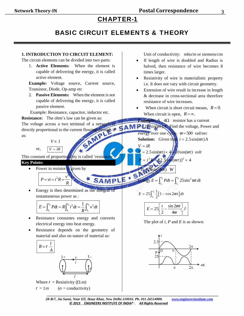
3CHAPTER-1
BASIC CIRCUIT ELEMENTS & THEORY
1. INTRODUCTION TO CIRCUIT ELEMENT:The circuit elements can be divided into two parts:
1. Active Elements: When the element iscapable of delivering the energy, it is calledactive element.
Example: Voltage source, Current source,Transistor, Diode, Op-amp etc2. Passive Elements: When the element is not
capable of delivering the energy, it is calledpassive element.
Example: Resistance, capacitor, inductor etc.Resistance: The ohm’s law can be given as:The voltage across a two terminal of a network isdirectly proportional to the current flowing through itas:
V I
or, V IR
This constant of proportionality is called ‘resistance’.Key Points: Power in resistor is given by
22 v
P vi i RR
Energy is then determined as the integral ofinstantaneous power as :
2 2 2
1 1 1
2 21t t t
t t tE Pdt R i dt v dt
R
Resistance consumes energy and convertselectrical energy into heat energy.
Resistance depends on the geometry ofmaterial and also on nature of material as:
lR
A
Where = Resistivity (.m)
= 1/ ( = conductivity)
Unit of conductivity: mho/m or siemens/cm If length of wire is doubled and Radius is
halved, then resistance of wire becomes 8times larger.
Resistivity of wire is materialistic propertyi.e. It does not vary with circuit geometry.
Extension of wire result in increase in length& decrease in cross-sectional area thereforeresistance of wire increases.
When circuit is short circuit means, 0.R When circuit is open, .R
Example: A 4 resistor has a current2.5sin( ) .i t A Find the voltage, Power and
energy over one cycle. 500 rad/secSolution: Given that 2.5sin( )i t A
V iR2.5sin( ) 4 10sin( )V t t volt
2 2[2.5 sin( )] 4P i R t
225sin ( )P t W
Energy2 2
1 1
225sint t
t tE Pdt t dt
2
1
125 1 cos 2
2
t
tE t dt
sin 225
2 4
t tE J
The plot of i, P and E is as shown:

Network Theory-IN Postal Correspondence
28-B/7, Jia Sarai, Near IIT, Hauz Khas, New Delhi-110016. Ph. 011-26514888. www.engineersinstitute.com© 2015 ENGINEERS INSTITUTE OF INDIA® . All Rights Reserved
4
This illustrate that P is always positive andthat the energy is always increasing. This isthe energy dissipated by resistor.
2. CAPACITANCE:The circuit element that stores energy in an electricfield is called capacitor. When variable voltage isapplied to a terminal of capacitor, the energy is storedduring one part of cycle and discharge during nexthalf cycle.The charge across the capacitor is directlyproportional to the applied voltage:
Q VQ CV
QC Unit of C Farad
V
Key Points:(a.) Capacitors retain the charge & thus
electric field after removal of the sourceapplied. (While inductors do not retainenergy). For parallel plate capacitor, thecapacitance can be given as:
o r AC
d
Where A = cross-sectional area of plate
r Relative permittivity of dielectric
o Permittivity of free space
d = distance between plates
8.854 r AC pF
d
(b.) The charge q on capacitor results in anelectric field in the dielectric which is themechanism of energy storage.
(c.) Power and energy relation for capacitanceare as:
21
2
dv dP vi vc cv
dt dt
cdvi
dt
21
2
dP cv
dt
Energy2 2
1 1
t t
c
t t
dvw P dt v c dt
dt
2 22 1
1
2cw c v v
(d.) The energy stored in the electric field of
capacitance is21
2cw cv
(e.) Ideal capacitor:
Practical capacitor:
Example: In the interval 0 > t > 5 ms, a 20 fcapacitor has a voltage 50sin 2( ) .V t V Obtain
the charge, power and energy. Plot work cw
assuming w = 0 at t = 0. 100 . / secrad Solution: 20 50sin 2q cv t
1000 sin 2q t C
0.2cos2dv
i c t Adt
50sin200 0.2cos2P vi t t 5sin 4P t W

Network Theory-IN Postal Correspondence
28-B/7, Jia Sarai, Near IIT, Hauz Khas, New Delhi-110016. Ph. 011-26514888. www.engineersinstitute.com© 2015 ENGINEERS INSTITUTE OF INDIA® . All Rights Reserved
5
2
1 0
5sin 400t t
ct
w P dt t dt
12.5 1 cos 400cw t mJ
This indicates that in the internal 0 > t > 2.5 ms, theenergy is stored to value of 25 mJ and then it returnsto zero, as the energy is returned to the source.
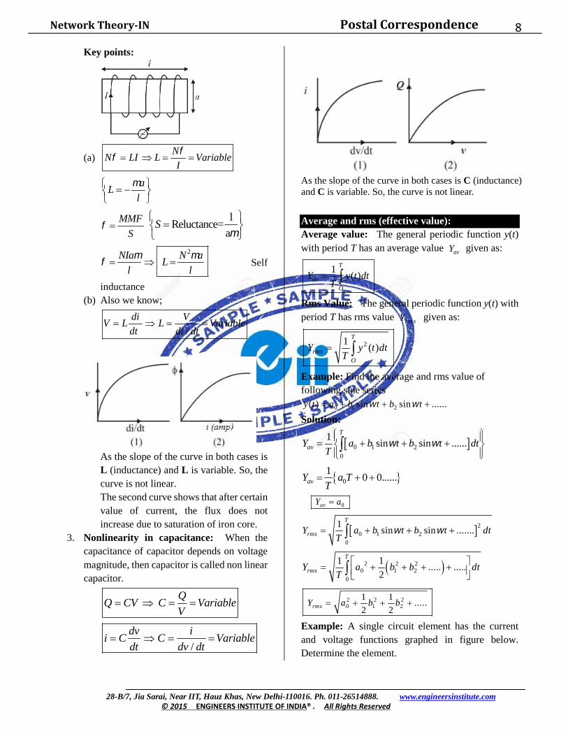
3. INDUCTANCE:The circuit element that stores energy in a magneticfield is called an inductor.
When voltage is applied across a inductor, the flux isinduced in the conductor which is proportional tocurrent flowing through it, i.e.
N i
N Li
NL
i
L Inductance
Unit HenryKey Points:
(a) The flux linkage across inductor is N. Thus
N LI
(b) Inductor do not store energy when theconnected source is removed
Voltage induced across the inductor is
diV L
dt ………….. (A)
{Voltage is induced when flux is varying}
(c) For an inductor of N no of turns:
20M N S
Ll
S = Cross sectional areal = Length of coil
(d) Proof of equation A: According tofaraday’s law, the emf induced across ainductor is directly proportional to the rateof change of flux through it.
de N
dt
{N = no of turns in the coil}
d LIe N
dt N
dIe L
dt
-ve sign indicates the opposition caused byemf to change of flux (Lenz’s Law)
(e) The power across the inductor is:
21
2
di dP vi L i Li
dt dt
(f) Energy:2 2
1 1
t t
t t
w P dt Li dt
2 22 1
1
2w L i i
Energy stored in magnetic field by inductor
is21
2w Li
Example:
In the interval 0 , 3050
t s a mH
inductance
has a current i=10sin50tA. Obtain the Voltage, Power& Energy for the inductance.

Network Theory-IN Postal Correspondence
28-B/7, Jia Sarai, Near IIT, Hauz Khas, New Delhi-110016. Ph. 011-26514888. www.engineersinstitute.com© 2015 ENGINEERS INSTITUTE OF INDIA® . All Rights Reserved
6
Solution: 15 cos 50di
v L t Vdt
75sin(100 )p vi t W
0 075sin100
0.75(1 cos100 )
t tw P dt t dt
w t J
The Plot indicate that the energy is zero at t = 0 and
sec.50
t Thus while energy transfer occurred over
the interval, this energy was first stored and laterreturned to the source.
Relationship of parameters:Element Units Voltage Current Power
Resistance
inductance
Capacitance
Ohms
()
Henry(H)
Farad(F)
v Ri (ohmslaw)
div Ldt
1v idtc
viR
1i vdtL
dvi cdt
2
P vi
i R
P viLdiidt
P vidvvcdt
Voltage & Current Source:The sources are of two types, one is independentsources and other is dependent sources:Independent sources:The voltage or current source in which the value ofvoltage or current remains constant, and does notvary with other circuit element.Ideal voltage and current sources:
Non ideal voltage and current sources:
(a) In non ideal voltage source, the internalresistance of voltage source is of finite valueand is always in series with voltage source.
(b) In non ideal current source, the internalresistance of current source is of finite value& is always in parallel with current source.
(c) V-source in series

Network Theory-IN Postal Correspondence
28-B/7, Jia Sarai, Near IIT, Hauz Khas, New Delhi-110016. Ph. 011-26514888. www.engineersinstitute.com© 2015 ENGINEERS INSTITUTE OF INDIA® . All Rights Reserved
7
(d)
(e)
Dependent Voltage and Current Sources:These are voltage and current sources whose value donot remain constant, rather varies with circuitelements or independent sources:
Distributed and Lumped Network:In Lumped network, we can separate resistance,inductance, and capacitance separately or singleelement in one location is used to represent adistributed resistance.Example: A coil having large number of turns ofinsulated wire has resistance throughout the length ofwire but only resistance at single plane represents thedistributed resistance.In Distributed network, the circuit elements are not atone location rather they are distributed.Example: Transmission line, the resistance,inductance and capacitance are distributedthroughout the length of Transmission line.Note: In distributed network, the circuit elementsare represented as per unit length.
Non Linearity of circuit elements:1. Resistance Non Linearity: If the current
voltage relationship in an element is notlinear, then the element is modeled as nonlinear resistor.Example: Diode, filament lamp (This athigher voltage droves proportional lesscurrent) etc.(a) The non linear resistance can be given as:
VR
I
Note: Ohm’s law is valid for linear circuitelements. Also it is not valid for open circuitelement because for open circuit:
I = 0, R = So V =
V IR
2. Inductors non linearity: When theinductance of inductor depends on thecurrent magnitude, then the inductor iscalled non linear inductor:Example: Iron core inductor.
Only air core inductor linear
Network Theory-IN Postal Correspondence
28-B/7, Jia Sarai, Near IIT, Hauz Khas, New Delhi-110016. Ph. 011-26514888. www.engineersinstitute.com© 2015 ENGINEERS INSTITUTE OF INDIA® . All Rights Reserved
8
Key points:
(a)N
N LI L VariableI
aL
l
MMF
S
lReluctance=
aS
2NIa N a
Ll l
Self
inductance(b) Also we know;
/
di VV L L Variable
dt di dt
As the slope of the curve in both cases isL (inductance) and L is variable. So, thecurve is not linear.The second curve shows that after certainvalue of current, the flux does notincrease due to saturation of iron core.
3. Nonlinearity in capacitance: When thecapacitance of capacitor depends on voltagemagnitude, then capacitor is called non linearcapacitor.
/
QQ CV C Variable
V
dv ii C C Variable
dt dv dt
As the slope of the curve in both cases is C (inductance)and C is variable. So, the curve is not linear.
Average and rms (effective value):Average value: The general periodic function y(t)with period T has an average value avY given as:
1( )
T
avO
Y y t dtT
Rms Value: The general periodic function y(t) withperiod T has rms value rm sY given as:
21( )
T
rmsO
Y y t dtT
Example: Find the average and rms value offollowing sine series
0 1 2( ) sin sin ......y t a b t b t
Solution:
0 1 20
1sin sin ......
T
avY a b t b t dtT
0
10 0......avY a T
T
0avY a
20 1 20
1sin sin .......
T
rmsY a b t b t dtT
2 2 20 1 2
0
1 1..... .....
2
T
rmsY a b b dtT
2 2 20 1 2
1 1.....
2 2rmsY a b b
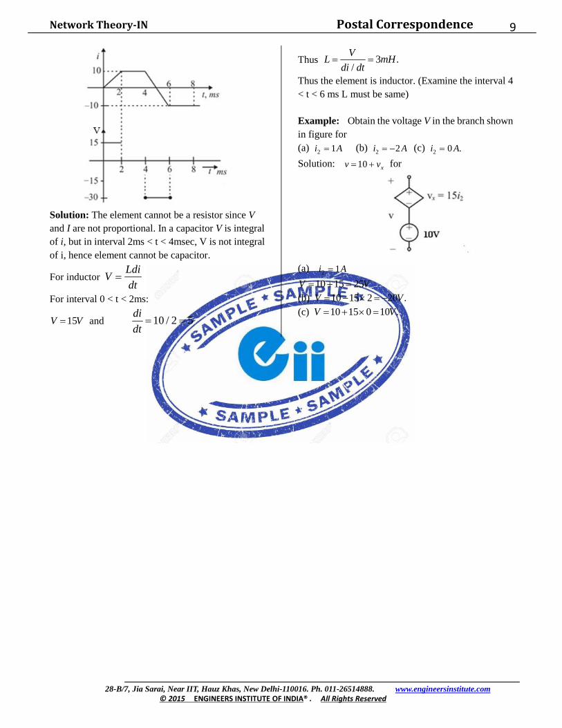
Example: A single circuit element has the currentand voltage functions graphed in figure below.Determine the element.
Network Theory-IN Postal Correspondence
28-B/7, Jia Sarai, Near IIT, Hauz Khas, New Delhi-110016. Ph. 011-26514888. www.engineersinstitute.com© 2015 ENGINEERS INSTITUTE OF INDIA® . All Rights Reserved
9
Solution: The element cannot be a resistor since Vand I are not proportional. In a capacitor V is integralof i, but in interval 2ms < t < 4msec, V is not integralof i, hence element cannot be capacitor.
For inductorLdi
Vdt
For interval 0 < t < 2ms:
15V V and 10 / 2 5di
dt
Thus 3 ./
VL mH
di dt
Thus the element is inductor. (Examine the interval 4< t < 6 ms L must be same)
Example: Obtain the voltage V in the branch shownin figure for(a) 2 1i A (b) 2 2i A (c) 2 0 .i A
Solution: 10 xv v for
(a) 2 1i A
10 15 25V V (b) 10 15 2 20 .V V (c) 10 15 0 10 .V V
Network Theory-IN Postal Correspondence
28-B/7, Jia Sarai, Near IIT, Hauz Khas, New Delhi-110016. Ph. 011-26514888. www.engineersinstitute.com© 2015 ENGINEERS INSTITUTE OF INDIA® . All Rights Reserved
10
CHAPTER-2
NETWORK LAWS AND THEOREMS
Control System-EE Postal Correspondence Course 11
Postal Course ( GATE & PSUs) © 2015 ENGINEERS INSTITUTE OF INDIA® . All Rights Reserved28-B/7, Jia Sarai, Near IIT, Hauz Khas, New Delhi-110016. Ph. 011-26514888. www.engineersinstitute.com
1. SOME BASIC TERMS:
1. Node: Any point in a circuit where the terminals of two or more elements are connected
together.
2. Branch: A branch is a part of circuit which extends from one node to other. A branch may
contain one element or several elements in series. It has two terminals.
3. Essential Node: If three or more elements are connected together at a node, then that node
sometimes called essential node.
4. Mesh: Any closed path which contains no other path within, called mesh.
5. Loop: A path which contain more than two meshes, called a loop. Thus a loop contains meshes
but a mesh does not contain loop.
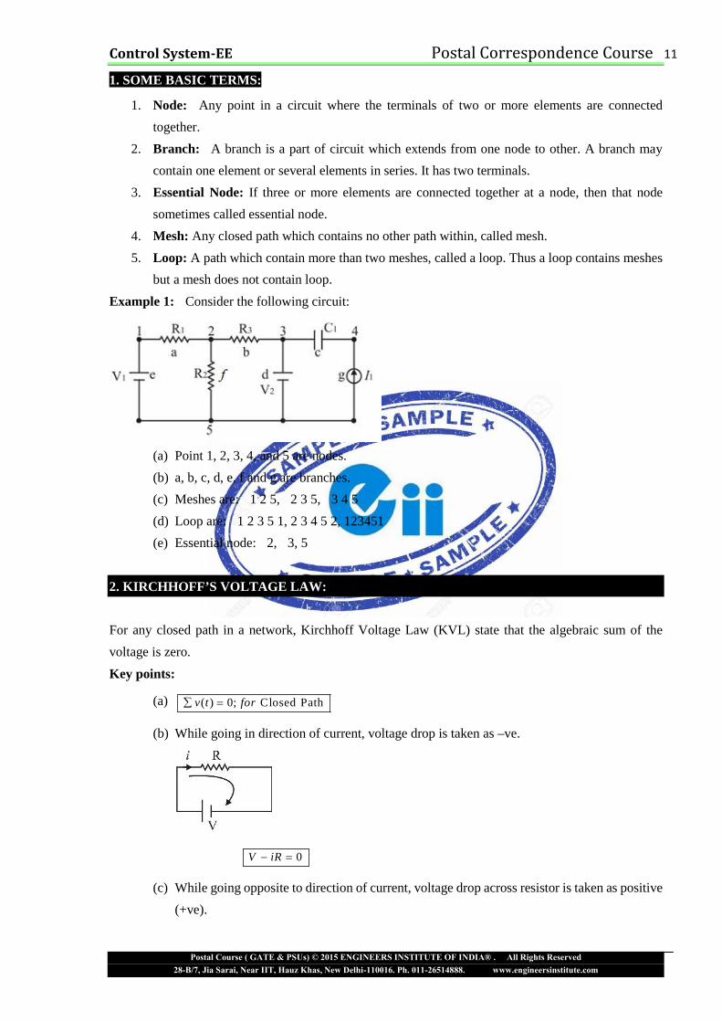
Example 1: Consider the following circuit:
(a) Point 1, 2, 3, 4, and 5 are nodes.
(b) a, b, c, d, e, f and g are branches.
(c) Meshes are: 1 2 5, 2 3 5, 3 4 5
(d) Loop are: 1 2 3 5 1, 2 3 4 5 2, 123451
(e) Essential node: 2, 3, 5
2. KIRCHHOFF’S VOLTAGE LAW:
For any closed path in a network, Kirchhoff Voltage Law (KVL) state that the algebraic sum of the
voltage is zero.
Key points:
(a) ( ) 0; Closed Pathv t for
(b) While going in direction of current, voltage drop is taken as –ve.
0V iR
(c) While going opposite to direction of current, voltage drop across resistor is taken as positive
(+ve).
Control System-EE Postal Correspondence Course 12
Postal Course ( GATE & PSUs) © 2015 ENGINEERS INSTITUTE OF INDIA® . All Rights Reserved28-B/7, Jia Sarai, Near IIT, Hauz Khas, New Delhi-110016. Ph. 011-26514888. www.engineersinstitute.com
0iR V
(d) This law applies equally to DC, time variable sources.
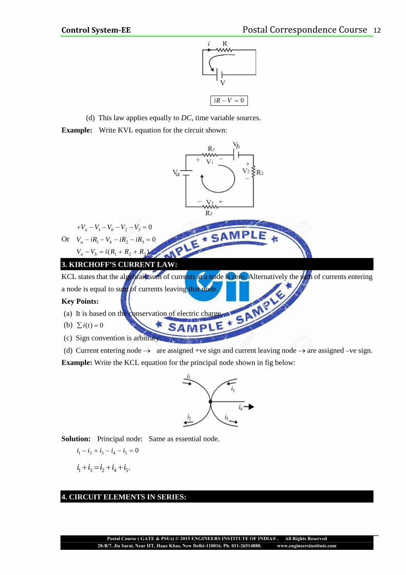
Example: Write KVL equation for the circuit shown:
1 2 3 0a bV V V V V
Or 1 2 3 0a bV iR V iR iR
1 2 3( )a bV V i R R R
3. KIRCHOFF’S CURRENT LAW:
KCL states that the algebraic sum of currents at a node is zero. Alternatively the sum of currents entering
a node is equal to sum of currents leaving that node.
Key Points:
(a) It is based on the conservation of electric charge.
(b) ( ) 0i t
(c) Sign convention is arbitrary.
(d) Current entering node are assigned +ve sign and current leaving node are assigned –ve sign.
Example: Write the KCL equation for the principal node shown in fig below:
Solution: Principal node: Same as essential node.
1 2 3 4 5 0i i i i i
1 3 2 4 5.i i i i i
4. CIRCUIT ELEMENTS IN SERIES:
Control System-EE Postal Correspondence Course 13
Postal Course ( GATE & PSUs) © 2015 ENGINEERS INSTITUTE OF INDIA® . All Rights Reserved28-B/7, Jia Sarai, Near IIT, Hauz Khas, New Delhi-110016. Ph. 011-26514888. www.engineersinstitute.com
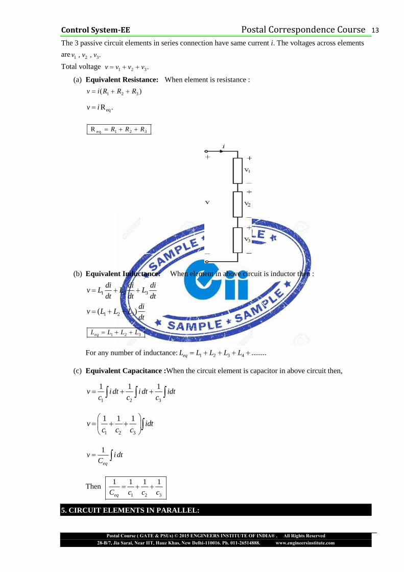
The 3 passive circuit elements in series connection have same current i. The voltages across elements
are 1 2 3, , .v v v
Total voltage 1 2 3 .v v v v
(a) Equivalent Resistance: When element is resistance :
1 2 3( )v i R R R
eqR .v i
eq. 1 2 3R R R R
(b) Equivalent Inductance: When element in above circuit is inductor then :
1 2 3
di di div L L L
dt dt dt
1 2 3( )di
v L L Ldt
1 2 3eqL L L L
For any number of inductance: 1 2 3 4 ........eqL L L L L
(c) Equivalent Capacitance :When the circuit element is capacitor in above circuit then,
1 2 3
1 1 1v i dt i dt idt
c c c
1 2 3
1 1 1v idt
c c c
1
eq
v i dtC
Then1 2 3
1 1 1 1
eqC c c c
5. CIRCUIT ELEMENTS IN PARALLEL:

Control System-EE Postal Correspondence Course 14
Postal Course ( GATE & PSUs) © 2015 ENGINEERS INSTITUTE OF INDIA® . All Rights Reserved28-B/7, Jia Sarai, Near IIT, Hauz Khas, New Delhi-110016. Ph. 011-26514888. www.engineersinstitute.com
The 3 element are connected as shown in figure
(a) Equivalent Resistance: 1 2 3i i i i
1 2 3
v v vi
R R R
1 2 3
1 1 1i v
R R R
Theneq 1 2 3
1 1 1 1
R R R R
(b) Equivalent Inductance :
1 2
1 1 1.....
eqL L L
For two inductance 1 2
1 2eq
L LL
L L
(c) Equivalent Capacitance :
1 2 ......eqC c c
This is of the same form as resistor in series.
6. VOLTAGE DIVISION:
A set of series-connected resistor is referred as a voltage divider.
This concept is applicable to n number of resistance.
Control System-EE Postal Correspondence Course 15
Postal Course ( GATE & PSUs) © 2015 ENGINEERS INSTITUTE OF INDIA® . All Rights Reserved28-B/7, Jia Sarai, Near IIT, Hauz Khas, New Delhi-110016. Ph. 011-26514888. www.engineersinstitute.com
11
2 3 1
22
1 2 3
Rv v
R R R
Rv v
R R R
In voltage divider, voltage across one branch
Resistance of that branch=Total voltage × .
total resistance
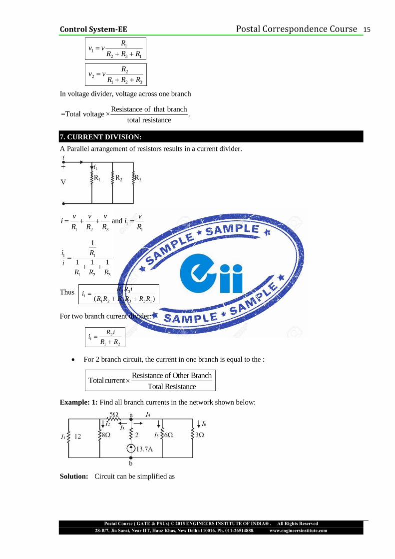
7. CURRENT DIVISION:
A Parallel arrangement of resistors results in a current divider.
11 2 3 1
andv v v v
i iR R R R
1 1
1 2 3
1
1 1 1i R
iR R R
Thus 2 31
1 2 2 3 3 1( )
R R ii
R R R R R R
For two branch current divider:
21
1 2
R ii
R R
For 2 branch circuit, the current in one branch is equal to the :
Resistance of Other BranchTotalcurrent
Total Resistance
Example: 1: Find all branch currents in the network shown below:
Solution: Circuit can be simplified as
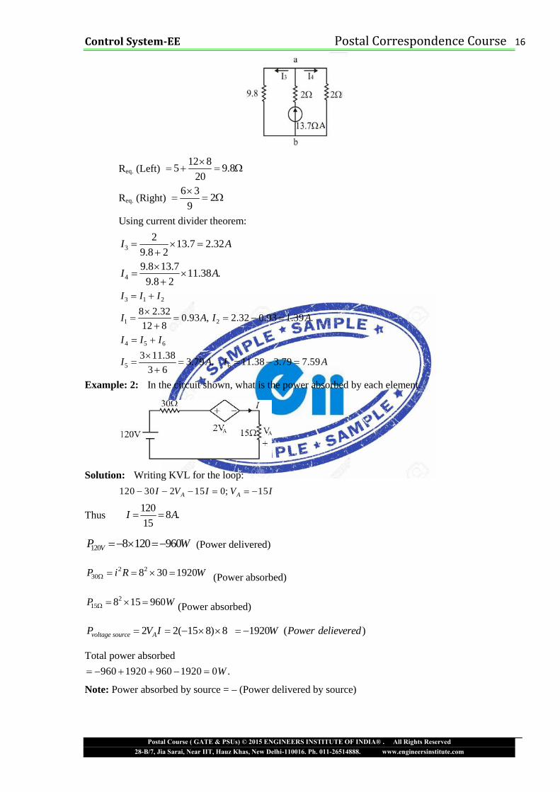
Control System-EE Postal Correspondence Course 16
Postal Course ( GATE & PSUs) © 2015 ENGINEERS INSTITUTE OF INDIA® . All Rights Reserved28-B/7, Jia Sarai, Near IIT, Hauz Khas, New Delhi-110016. Ph. 011-26514888. www.engineersinstitute.com
Req. (Left)12 8
5 9.820
Req. (Right)6 3
29
Using current divider theorem:
3
213.7 2.32
9.8 2I A
4
9.8 13.711.38 .
9.8 2I A
3 1 2
1 2
8 2.320.93 , 2.32 0.93 1.39 .
12 8
I I I
I A I A
4 5 6
5 6
3 11.383.79 . 11.38 3.79 7.59
3 6
I I I
I A I A
Example: 2: In the circuit shown, what is the power absorbed by each element.
Solution: Writing KVL for the loop:
120 30 2 15 0; 15A AI V I V I
Thus120
8 .15
I A
120 8 120 960VP W (Power delivered)
2 230 8 30 1920P i R W (Power absorbed)
215 8 15 960P W (Power absorbed)
2 2( 15 8) 8 1920 ( ) voltage source AP V I W Power delievered
Total power absorbed
960 1920 960 1920 0 .W
Note: Power absorbed by source = – (Power delivered by source)
Control System-EE Postal Correspondence Course 17
Postal Course ( GATE & PSUs) © 2015 ENGINEERS INSTITUTE OF INDIA® . All Rights Reserved28-B/7, Jia Sarai, Near IIT, Hauz Khas, New Delhi-110016. Ph. 011-26514888. www.engineersinstitute.com
77 Final Selections in Engineering Services 2014.Rank Roll Name Branch
1 171298 SAHIL GARG EE3 131400 FIRDAUS KHAN ECE6 088542 SUNEET KUMAR TOMAR ECE8 024248 DEEPANSHU SINGH EE
10 207735 VASU HANDA ECE22 005386 RAN SINGH GODARA ECE22 032483 PAWAN KUMAR EE29 070313 SAURABH GOYAL EE31 214577 PRAMOD RAWANI EE33 075338 DIPTI RANJAN TRIPATHY ECE35 003853 SHANKAR GANESH K ECE35 091781 KOUSHIK PAN EE36 052187 ANOOP A ECE37 008233 ARPIT SHUKLA ECE38 106114 MANISH GUPTA EE41 018349 VINAY GUPTA ECE44 098058 LEENA P MARKOSE EE45 029174 NAVNEET KUMAR KANWAT EE
9 Rank under AIR 100 in GATE 2015 ( Rank
6,8,19,28,41,56,76,91,98)
and many more.............................
To Buy Postal Correspondence Package call at
0-9990657855