Embed Size (px)
Citation preview
NeuromorphicCompu-ngintheHBP
SteveFurber(UniversityofManchester)
KarlheinzMeier(HeidelbergUniversity)
INNOVATIONWORKSHOPExploita-onofNeuromorphicCompu-ngTechnologies
3February2017,Brussels

2
Outline
• Neuromorphic Computing • international perspectives • in the Human Brain Project
• SpiNNaker • BrainScaleS • Innovation Roadmap
• applications

3
Outline
• Neuromorphic Computing • international perspectives • in the Human Brain Project
• SpiNNaker • BrainScaleS • Innovation Roadmap
• applications
4
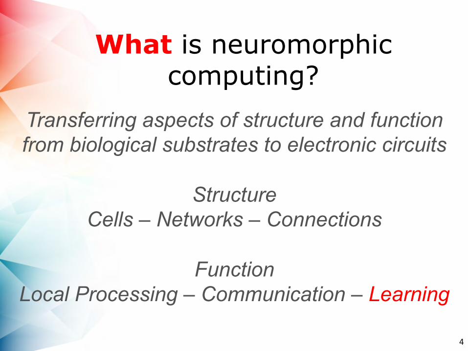
What is neuromorphic computing?
Transferring aspects of structure and function from biological substrates to electronic circuits
Structure
Cells – Networks – Connections
Function Local Processing – Communication – Learning
5
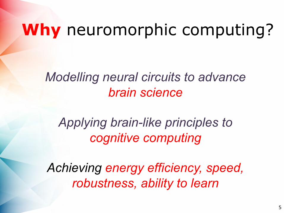
Why neuromorphic computing?
Modelling neural circuits to advance
brain science
Applying brain-like principles to cognitive computing
Achieving energy efficiency, speed,
robustness, ability to learn

http://www.technologyreview.com/featuredstory/526506/neuromorphic-chips/!
6
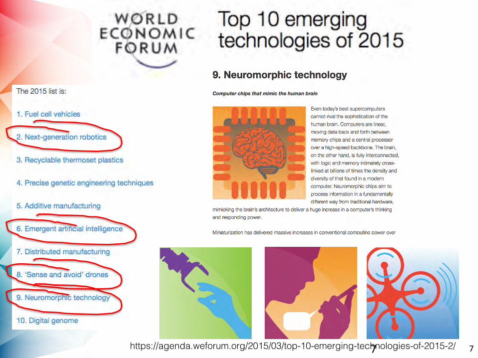
7https://agenda.weforum.org/2015/03/top-10-emerging-technologies-of-2015-2/! 7

REPORT TO THE PRESIDENT Ensuring Long-Term U.S.
Leadership in Semiconductors
Executive Office of the President President’s Council of Advisors on
Science and Technology
January 2017
8
Ensuring Long-Term U.S. Leadership in Semiconductors
28
Table A1. Selected component technology vectors that have a high probability of deployment in ten years (* denotes more speculative deployment within this timeframe)
Component technology vector
Time-frame to first commercial products
Approach to achieving and retaining competitive advantage
Neuromorphic Computing
Available now Continued R&D into new architectures coupled with 3D technologies and new materials, Deep Learning accelerators (for mobile and data center applications), and applications for true brain-inspired computing
Photonics Available now Foundries for tools and materials R&D; integrate photonics with CMOS and other materials
Sensors Available now Foundries for tools and materials R&D; integrate new types/classes of sensors with CMOS and other materials
CMOS (sub 7nm node size or new 3D structures)*
Advances in thermal management available with new process nodes
Deep understanding of transistor physics and chipset architecture and related design know-how; foundries and labs for transistor and materials R&D
Magnetics 1-2 years (MRAM as eFlash), 3 years (as DRAM), 5-7 years (as SRAM)
Foundries for tools and materials R&D; integrate magnetics with CMOS and other materials
3D 2-3 years (wafer-to-wafer stacking), 4-5 years (die-to-wafer stacking), 5-7 (Monolithic 3D)
Deep understanding of applications space and benefits associated use of 3D technologies and design know-how; foundries for tools and materials R&D; design automation tool R&D
Data-flow based architectures
3-4 years Continued architecture R&D, coupled with materials, integration, and manufacturing; build an ecosystem for solutions using data-flow based architectures
Ultra-high performance wireless systems
3 years (5G), 10-12 years (6G)
Continued R&D in new materials and processes, antenna design advances, chipset manufacturing, and integration
Advanced non-volatile memory as SRAM
5+ years Deep understanding of applications space and chipset architectures
Carbon nanotubes and phase change materials*
5-7 years Foundries/labs for materials R&D for hardware architectures; chipset designs to leverage these technologies
Biotech/human health
5-10 years R&D towards low power, highly integrated, high performance processing, high-data rate communications, wireless charging; couple R&D with clinical research to create, build, and evaluate on new materials and interfaces
Quantum Computing
< 10 years Pre-competitive R&D labs for new materials; foundries for new materials and hardware architectures; tools for quantum algorithms and software programming with various architectural paradigms
Point-of-Use Nanoscale 3D printing
Available now Desktop fab capabilities for rapid prototyping, additive manufacturing, moving beyond silicon and interfacing with soft matter, and small batch production
DNA for compute and storage*
10+ years Multi-disciplinary basic research in efficiently and reliably reading and writing and retrieving DNA strands
8
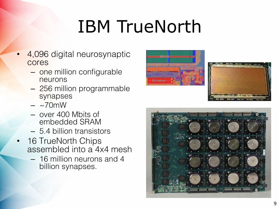
IBM TrueNorth • 4,096 digital neurosynaptic
cores!– one million configurable
neurons!– 256 million programmable
synapses!– ~70mW!– over 400 Mbits of
embedded SRAM!– 5.4 billion transistors!
• 16 TrueNorth Chips assembled into a 4x4 mesh!– 16 million neurons and 4
billion synapses. !
9

Stanford Neurogrid
• Neurocore Chip!– 65k neurons!– each with two
compartments and a set of configurable silicon ion channels!
• Sixteen Neurocores are assembled on a board!– million-neuron
Neurogrid!
10

11
HBP Neuromorphic Computing Concepts
PHYSICALMODELSYSTEM
Localanalogcompu-ngwith4Millionneuronsand50Millionsynapses–binary,asynchronouscommunica-on–
emula-onspeedisx10000real--me
Loca-on:Heidelberg(Germany)
MANY-CORENUMERICALMODELSYSTEM
0.5–1MillionARMprocessors–address-based,smallpacket,asynchronouscommunica-on–runningatreal--me
Loca-on:Manchester(UK)
12
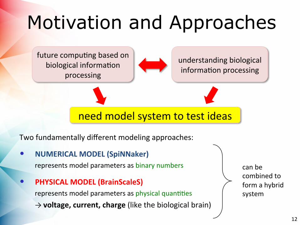
Motivation and Approaches futurecompu-ngbasedon
biologicalinforma-onprocessing
understandingbiologicalinforma-onprocessing
Twofundamentallydifferentmodelingapproaches:
• NUMERICALMODEL(SpiNNaker)representsmodelparametersasbinarynumbers
• PHYSICALMODEL(BrainScaleS)representsmodelparametersasphysicalquan--es→voltage,current,charge(likethebiologicalbrain)
canbecombinedtoformahybridsystem
needmodelsystemtotestideas
13
Outline
• Neuromorphic Computing • international perspectives • in the Human Brain Project
• SpiNNaker • BrainScaleS • Innovation Roadmap
• applications

SpiNNaker
14�

SpiNNaker
100kW15�
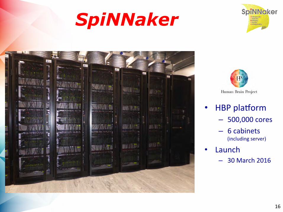
SpiNNaker
• HBPpladorm– 500,000cores– 6cabinets
(includingserver)
• Launch– 30March2016
16
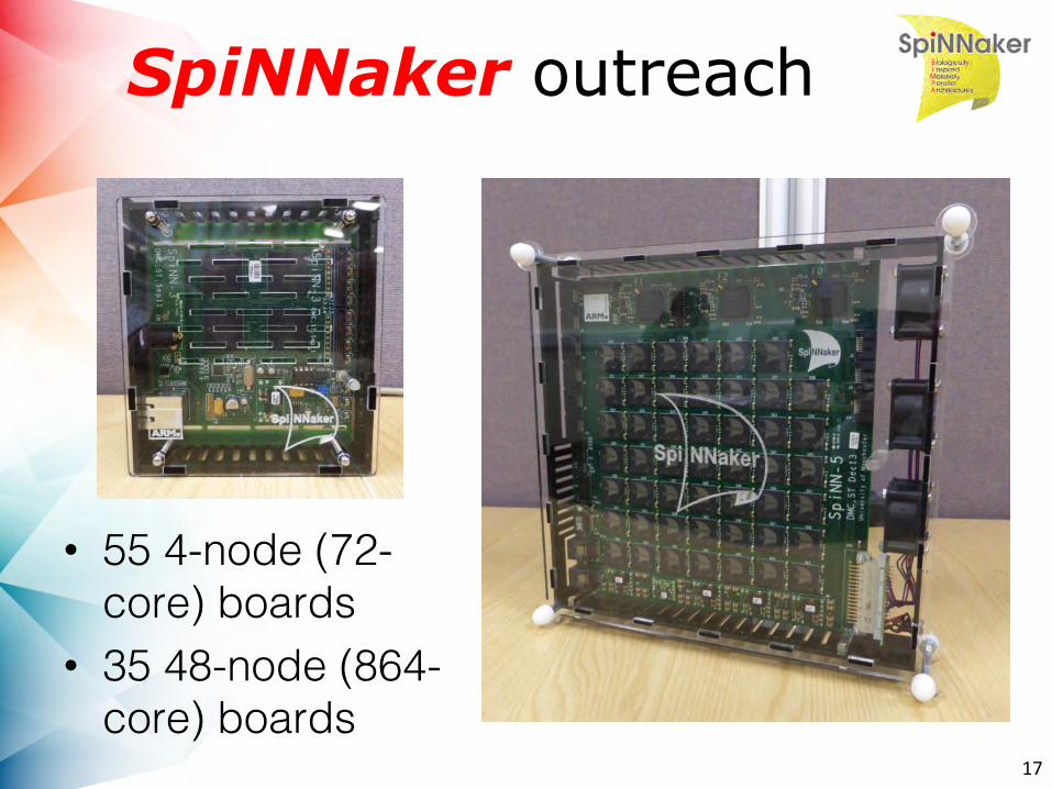
SpiNNaker outreach
17
• 55 4-node (72-core) boards!
• 35 48-node (864-core) boards!

SpiNNaker outreach
18
sales
loans

19
Multicast routing

20
Problem mapping

21
Outline
• Neuromorphic Computing • international perspectives • in the Human Brain Project
• SpiNNaker • BrainScaleS • Innovation Roadmap
• applications

PhysicalModelSystemCon-nuousTimeIntegra-ngNeuralCellMembrane
CmdVdt
= −gleak V −Eleak( ) Cm
R = 1/gleak
Eleak
V(t)
ΔV [V] gleak [S] Cm [F] (gΔV)/C [V/s]
Biology(*) 10-2 10-8 10-10 100 VLSI 10-1 10-6 10-13 106
(*) Brette/Gerstner, J. Neurophysiology, 2005
Inherent speed gap:
106 Volt/second → accelerated
neuron model
„Time“isimposedbyinternalphysics,notbyexternalcontrol
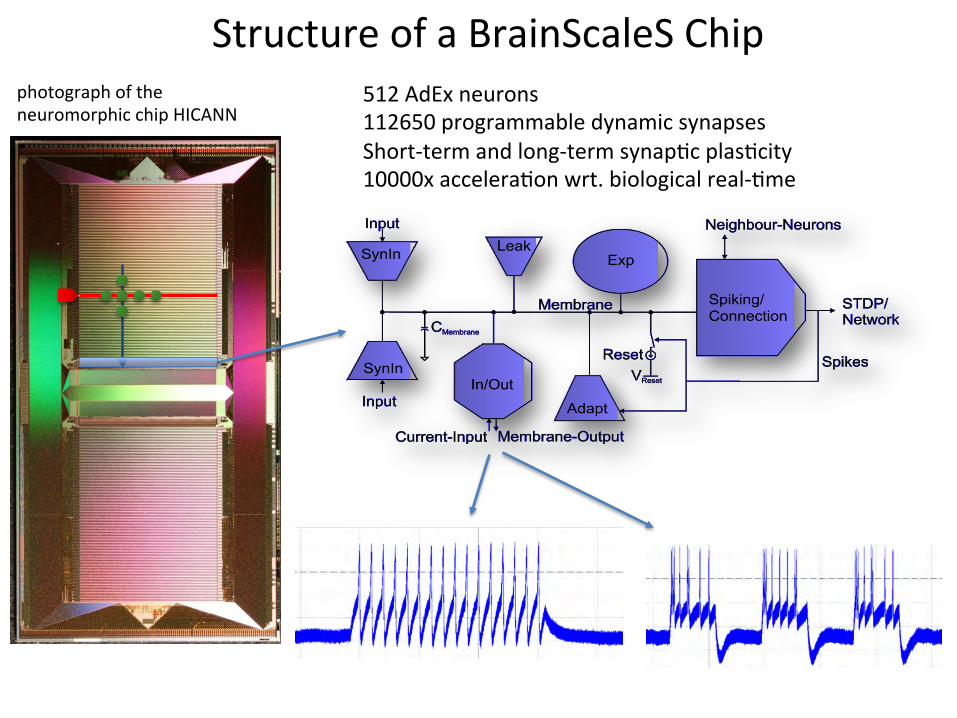
StructureofaBrainScaleSChipphotographoftheneuromorphicchipHICANN
512AdExneurons112650programmabledynamicsynapsesShort-termandlong-termsynap-cplas-city10000xaccelera-onwrt.biologicalreal--me

Centralelement20cmsiliconwaferwith450neuromorphicMicrochips
• analog,-me-con-nuousopera-on
• 10000fasterthanbiologicalreal-me
• 50Msynapseand230kneuroncircuitsoperateinparallel
• high-densityon-waferinterconnectsmanufacturedbymul--layerwafer-levelmetalliza-on

Physical Model, local analogue computing,
binary continuous time communication
Wafer-Scale Integration of 200.000 neurons and 50.000.000 synapses on
a single 20 cm wafer
Short term and long term plasticity, 10.000 faster
than real-time
Wafer-scaleintegra?onofanalogneuralnetworks,J.Schemmel,J,FieresandK.MeierIn:ProceedingsofIJCNN(2008),IEEEPress,431

Physical Model, local analogue computing,
binary continuous time communication
Wafer-Scale Integration of 200.000 neurons and 50.000.000 synapses on
a single 20 cm wafer
Short term and long term plasticity, 10.000 faster
than real-time
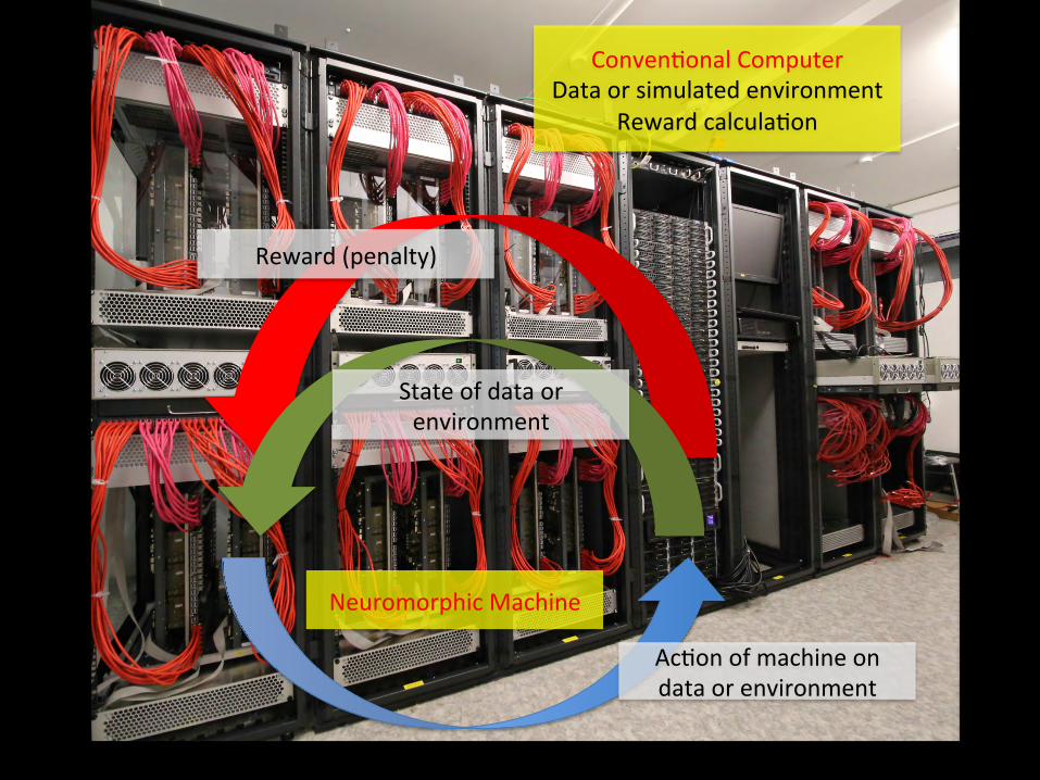
Conven-onalComputerDataorsimulatedenvironment
Rewardcalcula-on
Ac-onofmachineondataorenvironment
Stateofdataorenvironment
Reward(penalty)
NeuromorphicMachine
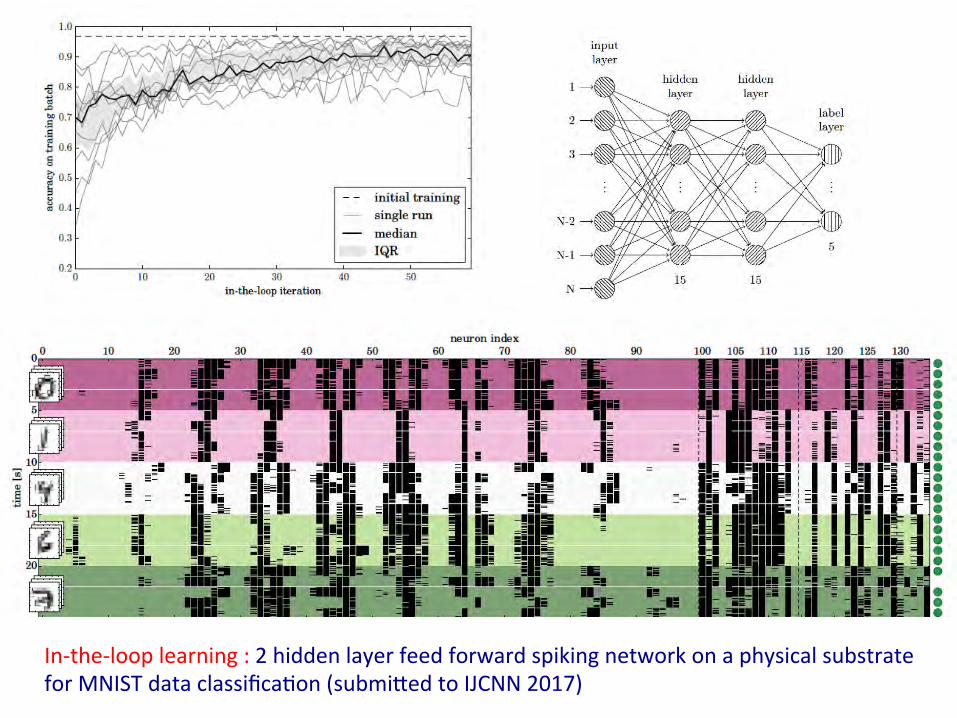
In-the-looplearning:2hiddenlayerfeedforwardspikingnetworkonaphysicalsubstrateforMNISTdataclassifica-on(submijedtoIJCNN2017)

NEST
model.py Data
NEURONSpiNNakerBrainScaleS
PyNN
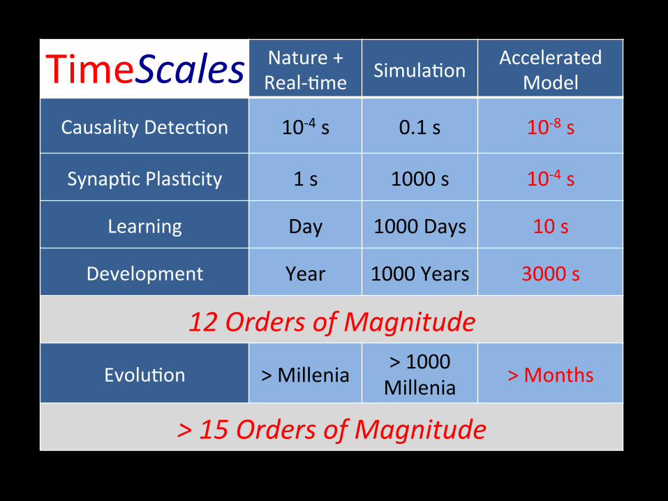
Nature+Real--me Simula-on Accelerated
Model
CausalityDetec-on 10-4s 0.1s 10-8s
Synap-cPlas-city 1s 1000s 10-4s
Learning Day 1000Days 10s
Development Year 1000Years 3000s
12OrdersofMagnitude
Evolu-on >Millenia >1000Millenia >Months
>15OrdersofMagnitude
TimeScales

31
Outline
• Neuromorphic Computing • international perspectives • in the Human Brain Project
• SpiNNaker • BrainScaleS • Innovation Roadmap
• applications
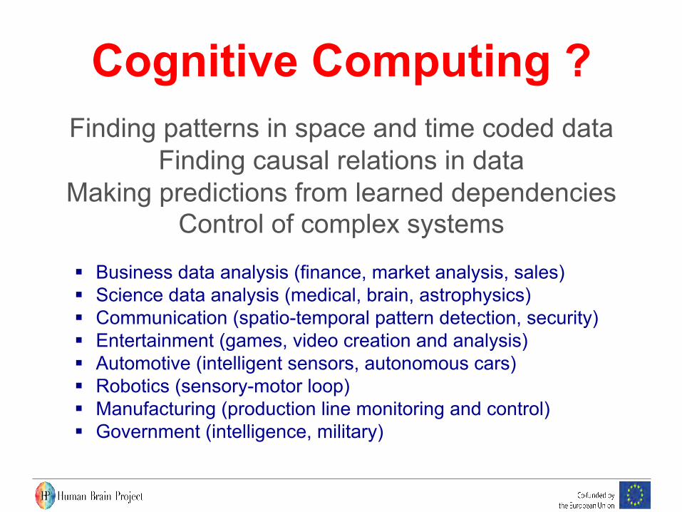
Cognitive Computing ?
Finding patterns in space and time coded data Finding causal relations in data
Making predictions from learned dependencies Control of complex systems
§ Business data analysis (finance, market analysis, sales) § Science data analysis (medical, brain, astrophysics) § Communication (spatio-temporal pattern detection, security) § Entertainment (games, video creation and analysis) § Automotive (intelligent sensors, autonomous cars) § Robotics (sensory-motor loop) § Manufacturing (production line monitoring and control) § Government (intelligence, military)
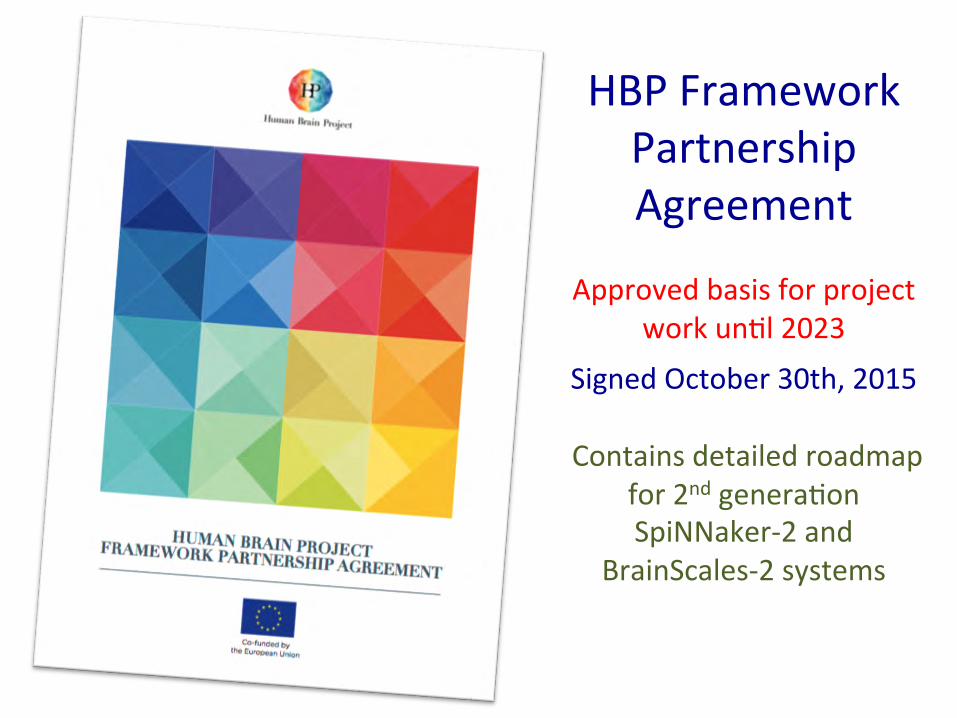
HBPFrameworkPartnershipAgreement
Approvedbasisforproject
workun-l2023
SignedOctober30th,2015
Containsdetailedroadmapfor2ndgenera-onSpiNNaker-2and
BrainScales-2systems

Processing Element
Processing Element
Processing Element
Processing Element
Rout
er
SerDesSerDesSerDes
SerDes SerDes SerDes SerDes
MCU
Memory Interface
Shared Memory
Shared Memory
Ongoing2ndgenera-onprototypedevelopmentStromgemphasisonlearningcapabili-es
SpiNNaker-2PowerManagementFloa-ngpointprecisionTruerandomnumbers
BrainScales-2PowerPCplas-cityprocessorsImprovedparameterstorage
Ac-vedendrites/compartments
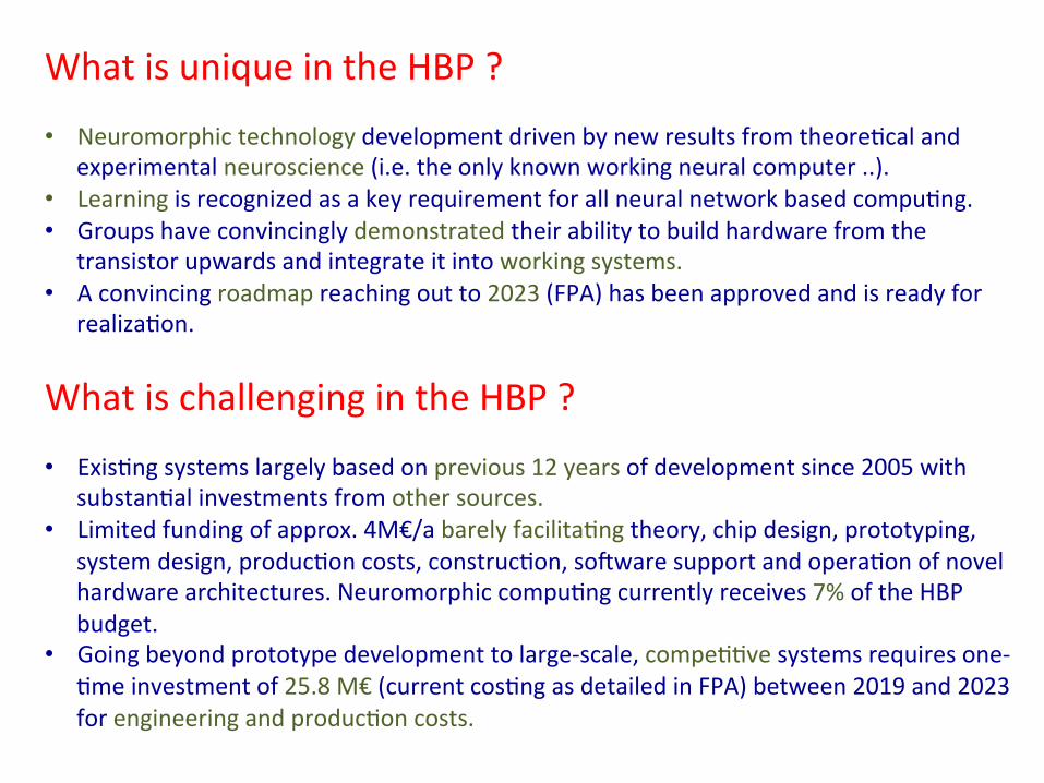
WhatisuniqueintheHBP?• Neuromorphictechnologydevelopmentdrivenbynewresultsfromtheore-caland
experimentalneuroscience(i.e.theonlyknownworkingneuralcomputer..).• Learningisrecognizedasakeyrequirementforallneuralnetworkbasedcompu-ng.• Groupshaveconvincinglydemonstratedtheirabilitytobuildhardwarefromthe
transistorupwardsandintegrateitintoworkingsystems.• Aconvincingroadmapreachingoutto2023(FPA)hasbeenapprovedandisreadyfor
realiza-on.
WhatischallengingintheHBP?• Exis-ngsystemslargelybasedonprevious12yearsofdevelopmentsince2005with
substan-alinvestmentsfromothersources.• Limitedfundingofapprox.4M€/abarelyfacilita-ngtheory,chipdesign,prototyping,
systemdesign,produc-oncosts,construc-on,sorwaresupportandopera-onofnovelhardwarearchitectures.Neuromorphiccompu-ngcurrentlyreceives7%oftheHBPbudget.
• Goingbeyondprototypedevelopmenttolarge-scale,compe--vesystemsrequiresone--meinvestmentof25.8M€(currentcos-ngasdetailedinFPA)between2019and2023forengineeringandproduc-oncosts.

Requiredstepstowardsexploita-onandapplica-on• Reinforceneuromorphiccompu-ngasakeycomponentofinnova-onemergingfrom
theHBPasaFETproject.Enablecon-nuedprototypedevelopmentaccordingtoFPAroadmap.
• Realizeengineeringandproduc-oncostsfor2ndgenera-onHBPsystemsaccordingtoFPAroadmap.
• Iden-fyspecificapplica-oncasesthroughexpressionsofinterests(EoIs)betweenHBPgroupsandindustrypartners.
• EvaluateEoIsandprovideECsupportforindustrialprototypedevelopmentofapplica-ons
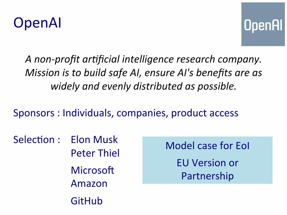
OpenAI
Anon-profitar?ficialintelligenceresearchcompany.MissionistobuildsafeAI,ensureAI'sbenefitsareas
widelyandevenlydistributedaspossible.
Sponsors:Individuals,companies,productaccessSelec-on: ElonMusk
PeterThiel
Microsor Amazon
GitHub
ModelcaseforEoI
EUVersionorPartnership

Click to edit Master title style • Click to edit Master text styles
– Secondlevel• Third level
– Fourth level
SpiNNaker-2 Chip Roadmap
SGA2 and SGA3
SpiNNaker2 • 68 ARM M4 cores • Power management • SpiNNaker router with SerDes • HMC interface • Chip Size: 70mm², >1 billion transistors
2015
2013
2014
2016
2017
2018
2019
2020
2021
2022
NanoLink28 • SerDes Transceiver • Chip Size: 4mm²
Santos28 • 4 ARM M4 cores • AVFS, DVFS power management • SpiNNaker router with SerDes • LPDDR2 Memory Interface • Chip Size: 18mm²
Nanolink28_gen2 • 2nd Iteration SerDes • HMC Interface
SGA1
SGA1 Nanolink28_gen3 • Final SerDes • Final HMC Interface
2023
Next generation chips and small prototype systems in SGA1 and SGA2 No secured funding for next generation large-scale systems
Click to edit Master title style
• Click to edit Master text styles – Secondlevel
• Third level
– Fourth level
> SGA
1
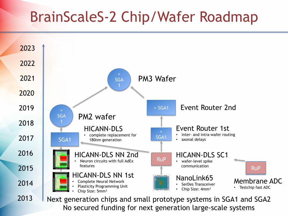
BrainScaleS-2 Chip/Wafer Roadmap
2015
2013
2014
2016
2017
2018
2019
2020
2021
2022
HICANN-DLS NN 1st • Complete Neural Network • Plasticity Programming Unit • Chip Size: 5mm²
NanoLink65 • SerDes Transceiver • Chip Size: 4mm²
RuP
Membrane ADC • Testchip fast ADC
RuP HICANN-DLS NN 2nd • Neuron circuits with full AdEx
features
HICANN-DLS SC1 • wafer-level spike
communication
> SGA1
> SGA1
> SGA
1
Event Router 1st • inter- and intra-wafer routing • axonal delays
Event Router 2nd
HICANN-DLS • complete replacement for
180nm generation
PM2 wafer
PM3 Wafer
2023
SGA1
Next generation chips and small prototype systems in SGA1 and SGA2 No secured funding for next generation large-scale systems

Click to edit Master title style
• Click to edit Master text styles – Secondlevel
• Third level
– Fourth level
Option : Novel Wafer-Level Packaging Technologies
reduce system complexity by embedding the wafer within
the printed circuit board
PressplatePresspadandsepara-onfoilCufoil5µmWaferandFR4frameCufoil5µmPresspadandsepara-onfoilPressplate
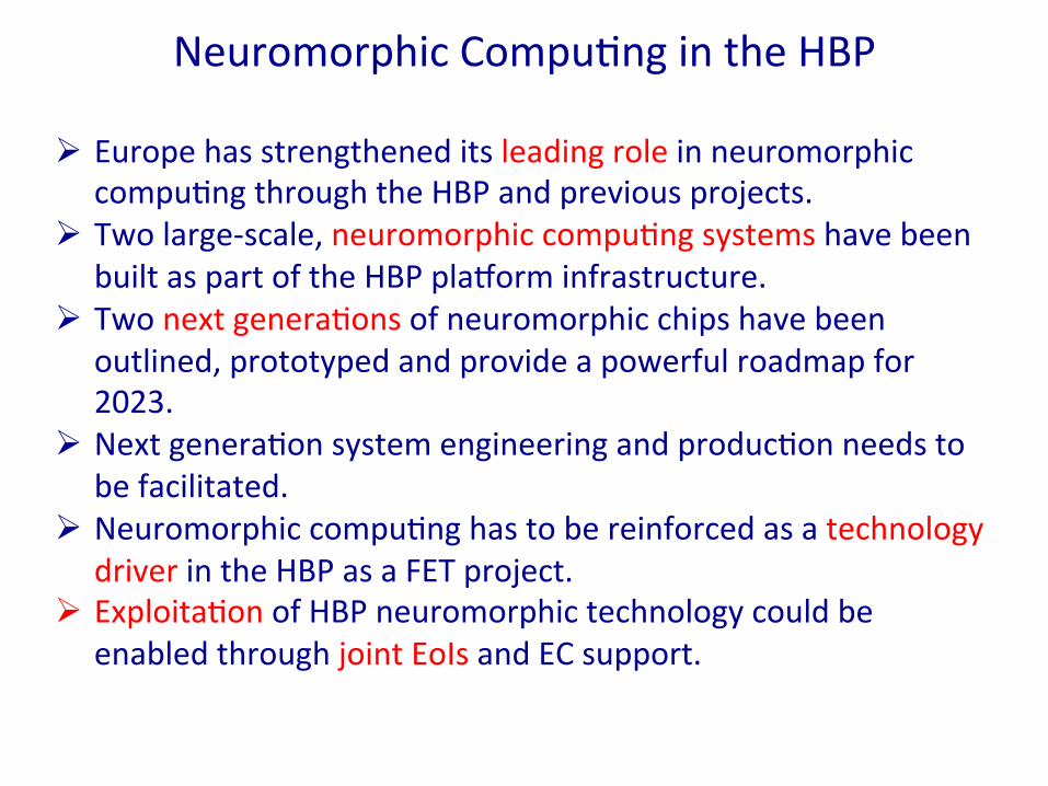
NeuromorphicCompu-ngintheHBP
Ø Europehasstrengtheneditsleadingroleinneuromorphiccompu-ngthroughtheHBPandpreviousprojects.
Ø Twolarge-scale,neuromorphiccompu-ngsystemshavebeenbuiltaspartoftheHBPpladorminfrastructure.
Ø Twonextgenera-onsofneuromorphicchipshavebeenoutlined,prototypedandprovideapowerfulroadmapfor2023.
Ø Nextgenera-onsystemengineeringandproduc-onneedstobefacilitated.
Ø Neuromorphiccompu-nghastobereinforcedasatechnologydriverintheHBPasaFETproject.
Ø Exploita-onofHBPneuromorphictechnologycouldbeenabledthroughjointEoIsandECsupport.

NeuromorphicCompu-ngGuidebook–Con-nuousUpdates
Comprehensiveopenaccessdocumenta-on:Hardware,systems,firmware,low/highlevelsorwareBenchmarks(neuroscience,machinelearning,SP11.3)Tutorials,smallsystems
hjp://neuromorphic.eu