Embed Size (px)
Citation preview
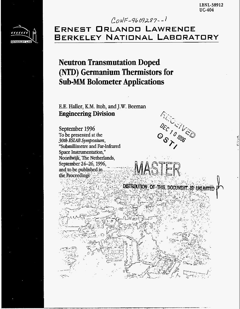
LBNL-38912 UC-404
@od1=-%DqG287- - 1 ERNEST ORLANDO LAWRENCE B E R KE LEY N AT I o N AL LAB o RATO RY
Neutron Transmutation Doped (NTD) Germanium Thermistors for SublMM Bolometer Applications
E.E. Haller, K.M. Itoh, and J.W. Beeman Engineering Division
September 1996 To be presented at the 30tb ESLAB Symposium, “Submiilimetre and Far-Infrared Space Instrumentation,” Noorili%ik, The Netherlands, ..
i *: ,- . .
k
DISCLAIMER
This document was prepared as an account of work sponsored by the United States Government. While this document is believed to contain correct information, neither the United States Government nor any agency thereof, nor The Regents of the University of California, nor any of their employees, makes any warranty. express or implied, or assumes any legal responsibility for the accuracy, completeness, or usefulness of any information, apparatus, product, or process disclosed. or represents that its use would not infringe privately owned rights. Reference herein to any specific commercial product, process, or service by its trade name, trademark, manufacturer. or otherwise, does not necessarily constitute or imply its endorsement, recommendation, or favoring by the United States Government or any agency thereof, or The Regents of the University of California. The views and opinions of authors expressed herein do not necessarily state or reflect those of the United States Government or any agency thereof, or The Regents of the University of California.
Ernest Orlando Lawrence Berkeley National Laboratory is an equal opportunity employer.
LBNL-389 12 uc-404
Neutron Transmutation Doped (Ntd) Germanium Thermistors for Sub-Mm Bolometer Applications
E.E. Hallerl.2 K.M. Itoh,3 and J.W. Beeman2
luniversity of California Berkeley, California 94720
2Engineering Division Emest Orlando Lawrence Berkeley National Laboratory
University of California Berkeley, California 94720
3Department of Instrumental Engineering Keio University
Yokohama, 223 Japan
September 1996
This work was supported by U.S. NASA under Contract Nos. W14606,16404,16164, and 17605 through interagency agreements with the U.S. Department of Energy under Contract No. DE-AC03-76SF00098.
DISCLAIMER
Portions of this document may be illegible in electronic image products. Images are produced from the best available. original document.
LBNL~38912 30th ESLAB Symposium, "Submillimetre and Far-Infmed Space Instrumentation," N C K N ~ W ~ J ~ The Netherlands, Sept 24-26,1996
NEUTRON TRANSMUTATION DOPED (NTD) GERMANIUM THERMISTORS FOR SUB-MM BOLOMETER APPLICATIONS
E.E. HalIer1.2, KM, Itoh3 and J.W. Beeman2
University of California at Berkeley, Berkeley, CA 94720 USA, Lawrence Berkeley National Laboratory, Berkeley, CA 94720 USA and Dept of Instr. Eng., Keio Univ. , Yokohama, 223 JAPAN
[email protected], Phone (510) 486-5294, FAX (510) 486-5530
ABSTRACT
We report on recent advances in the development of Neutron Transmutation Doped (NTD) semiconductor thermistors fabricated from Germanium of natural and controlled isotopic composition. The near ideal doping uniformity which can be achieved with the NTD process, the device simplicity of NTD Ge thermistors and the high performance of cooled junction field effect transistor (FET) preamplifiers have led to the widespread acceptance of these thermal sensors in many radiotelescopes operating on the ground, on high altitude aircraft and on spaceborne satellites. These features also have made possible the development of efficient bolometer arrays which are beginning to produce exciting results.
1. INTRODUCTION
Detection of electromagnetic radiation the mm and near mm wavelength range continues to pose a challenge, especially for high ,performance applications in low photon backgrounds. The invention of the semiconductor thermistor [l] and subsequently of broadband composite bolometers by Coron (21, which were optimized by Nishioka et al. [3], has led to widespread use of these sensors in recent years on many radiotelescopes.
The introduction of Neutron Transmutation Doped (NTD) Germanium thermistors [4] has put thermistor research and development on a f m scientific and solid engineering footing. This has stimulated the development of bolometer arrays reaching pixel numbers of close to 100. There are no fundamental limitations to further improvement of bolometer performance. Lower operating temperatures, a reduction of the bolometer heat capacity, improved bolometer array mounting schemes and efficient coupling of the radiation to the bolometer are among the major ingredients for higher performance devices. '
'In the following we will review the NTD process 'and point out its advantages over conventional doping techniques. The availability of isotopically controlled Germanium offers new opportunities for thermistor design. The major aspects of array developments will be mentioned, but for further details the reader is referred to
the relevant papers in these proceedings (W. Gear et al., E. Kreysa et al.). We will not discuss preamplifier issues which are complex and require most careful attention. One can state that in optimized systems the preamplifiers should not limit the performance of single element bolometers or of anays.
2 THE NTD PROCESS AND THERMISTOR FABRICATION
The low operating temperatures required for high performance bolometers make it necessary to use rather highly doped semiconductors for the sensing element, the thermistor. At typical operating temperatures of below lK, thermal activation of donor (acceptor) bound electrons (holes) no longer occurs at a rate sufficient to produce carrier concentrations which lead to resistivities of a few M IR cm. Such resistivities are required for the fabrication of optimized thermistors. Rather, the semiconductor becomes an excellent insulator when lightly doped. A new conduction regime is observed when doping in Ge reaches concentrations of 2 1015 ~ m - ~ . In this mode, bound carriers hop from one dopant atom to a nearby empty neighbor dopant atom. The probability for hopping to occur depends exponentially on the inter-dopant distance since we deal with a tunneling process.
This distance shows a normal distribution in a truly randomly doped semiconductor. Any fluctuations in the average local dopant concentration (often referred to as "dopant striations" in melt doped crystals [5] ) will lead to a change in the distribution of the inter-dopant distance which in turn will lead to fluctuations in the local hopping probability. Resistivity fluctuations over many orders of magnitude can easily result from + t h v doping striations as has been shown in experiments with Si thermistors [SI. What is required is a doping process which leads to a huly homogenous random distribution of donors and acceptors. Neither melt doping, doping during epitaxial growth, dopant diffusion nor ion implantation, all commonly used semiconductor doping processes, lead to the required uniformity.
The only process which guarantees this homogeneity is based on a process in which individual Ge atoms in a very pure and structurally perfect crystal are transmuted into
dopant atoms. Natural Ge is poly-isotopic and of its five stable isotopes (A = 70,72,73,74,76) three transmute to dopants after they have captured a thermal neutron in their nucleus [7]:
7oGe+n+ 71Ge + 71Ga+ve (1) 32 32 ?.l/,=ll.2d 31
- 74Ge+n+ 75Ge B 3 75AS+ve (2) 32 32 T1/~=82.8min 33 .
In reaction (1) Ga acceptors form whiIe reactions (2) and (3) lead to donors and double donors, respectively. Homogeneity of doping is intrinsic to the NTD process because the following three conditions are fullill&
- The stable isotopes in natural Ge are randomly distributed because they are chemically identical and none of the standard crystal growth processes are sensitive to the small nuclear mass fluctuations between the various isotopes.
- The thermal neutron sources used in NTD are very large compared to the size of semiconductor crystals.
- The absorption cross sections for neutron capture are very small (a few barns (10-24 cm2)) resulting in negligible "self" shadowing of the neutron flux inside the semiconductor.
Any neutron flux fluctuations vary very slowly with distance resulting in quasi-constant doping through rather large semiconductor crystals. Indeed, the Silicon power device industry uses several hundred tons of NTD Floating Zone 0 Si in order to obtain high yields in the production of silicon controlled rectifiers (SCR) and other high voltage devices. 181 The obvious problems related to NTD are radiation damage and nuclear transformation caused by residual high energy neutrons. The former problem is solved by appropriate thermal annealing (in Ge 400'C for 6 hrs) while the latter is hard to avoid. Fortunately a thorough study by Alessandrello et al. 191 has shown that the production of the radioactive 68Ge and 65Zn is totally negligible for radioastronomy applications of NTD Ge thermistors in composite bolometers.
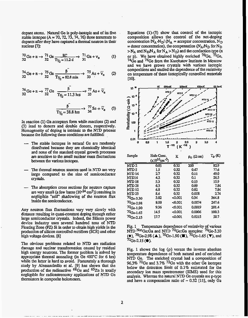
Equations (1)-(3) show that control of the isotopic composition allows the control of the net-doping concentration INA-NDI (NA = acceptor concentration, ND = donor concentration), the compensation (NAND for ND >NA a n d N d A forNA>ND)andtheconduction type (n or p). We have obtained highly enriched 70Ge, 73Ge, 74Ge and 76Ge from the Kurchatov Institute in Moscow and we have grown crystals with various isotopic compositions and studied the dependence of the resistivity on temperature of these isotopically controlled materials [lo].
Sample HoleConc. K po (am) To 6) (x1~16m -3)
NTD 2 0.03 0.32 200 829 NTD5 15 0.32 0.47 77.6 NTD 14 27 0.32 0.1 1 49.0 NTD16 4.2 0.32 0.1 265 NTD 18 5.3 0.32 0.15 15.9 NTD28 6.3 032 0.09 7.84 NTD 12 6.8 0.32 0.02 7.84 NTD25 8.6 0.32 0.008 274 70Ge-330 3.02 <0.001 034 364.8 7oGe-2.98 8.00 <0.001 0.0074 247.6 70Ge-1.90 936 <0.001 0.0019 201.4
70Ge-2.15 17.7 <0.001 0.0215 20.7 70Ge-1.65 145 <0.001 o.oO06 100.3
Fig. 1 Temperature dependence of resistivity of various NTD NatGe:Ga and NTD 7oGe:Ga samples: 70Ge3.30 (+), 70Ge2.98 (A), 70Ge-1.90 (M). 70Ge1.65 (V), and 70Ge2.15 (0).
Fig. 1 shows the log (p) versus the inverse absolute temperature dependence of both natural and of enriched NTD Ge. The enriched crystal had a composition of 96.3% 70Ge and 3.7% 72Ge with the other Ge isotopes below the detection limit of 0.1% estimated for the secondary ion mass spectrometer (SIMS) used for this analysis. Whereas the natural MTD Ge crystals are p-type and have a compensation ratio of - 0.32 [ll], only Ga
2
acceptors will form in 70Ge during NTD. The compensation will be dominated by residual chemical donors which are in the material before NTD. This donor concentration is of the order of 10l2 as determined by variable temperature Hall effect measurements of the undoped 7OGe crystals. The major interesting finding is that the resistivity appears to obey the simple dependence derived by Shklovskii and Efk6s 1121:
P =Po exp (4)
for the very wide range of compensation from the ~ h l r a l NTD Ge (0.32) to the heavily-doped NTD 70Ge samples (0.001). The resistivity of all 70Ge samples depends more strongly on temperature than the corresponding natural NTD Ge crystals. This difference is especially pronounced for the lightly doped samples with resistivities between lo4 and lo7 i2 cm in the 0.5 to 1K range.
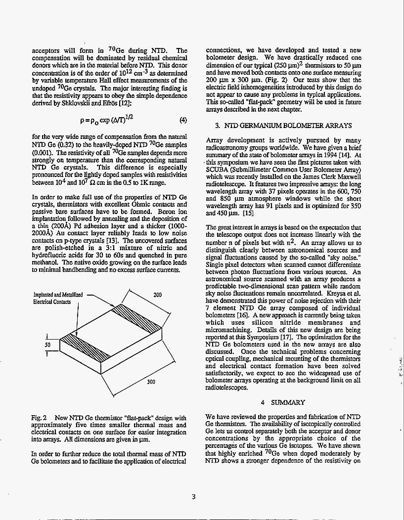
In order to make full use of the properties of NTD Ge crystals, thermistors with excellent Ohmic contacts and passive bare surfaces have to be formed. Boron ion implantation followed by annealing and the deposition of a thin (200A) Pd adhesion layer and a thicker (1000- 2000A) Au contact layer reliably leads to low noise contacts on p-type crystals [13]. The uncovered surfaces are polish-etched in a 3:l mixture of nitric and hydrofluoric acids for 30 to 60s and quenched in pure methanol. The native oxide growing on the surface leads to minimal bandbending and no excess surface currents.
Elccbical Contacts
Fig. 2 New NTD Ge thermistor "flat-pack" design with approximately five times smaller thermal mass and electrical contacts on one surface for easier integration into arrays. AlI dimensions are given in pm.
In order to further reduce the total thermal mass of NTD Ge bolometers and to facilitate the application of electrical
connections, we have developed and tested a new bolometer design. We have drastically reduced one dimension of our typical (250 thermistors to 50 pm and have moved both contacts onto one surface measuring 200 pm x 300 pm. (Fig. 2) Our tests show that the electric field inhomogeneities introduced by this design do not appear to cause any problems in typical applications. This so-called "flat-pack" geometry will be used in future arrays described in the next chapter.
3. NTD GERMANIUM BOLOMETER ARRAYS
Array development is actively pursued by many radioastronomy groups worldwide. We have given a brief summary of the state of bolometer arrays in 1994 [14]. At
. this symposium we have seen the first pictures taken with SCUBA (Submillimeter Common User Bolometer Array) which was recently installed on the James Clerk Maxwell radiotelescope. It features two impressive arrays: the long wavelength array with 37 pixels operates in the 600,750 and 850 pm atmosphere windows while the short wavelength array has 91 pixels and is optimized for 350 and450pm. [la The great interest in arrays is based on the expectation that the telescope output does not increase linearly with the number n of pixels but with n2. An array allows us to distinguish clearly between astronomical sources and signal fluctuations caused by the so-called "sky noise." Single pixel detectors when scanned cannot differentiate between photon fluctuations from various sources. An astronomical source scanned with an array produces a predictable two-dimensional scan pattern while random sky noise fluctuations remain uncorrelated. Kreysa et al. have demonstrated this power of noise rejection with their 7 element NTD Ge array composed of individual bolometers (161. A new approach is currently being taken which uses silicon nitride membranes and micromachining. Details of this new design are being reported at this Symposium [17]. The optimization for the NTD Ge bolometers used in the new arrays are also discussed. Once the technical problems concerning optical coupling, mechanical mounting of the thermistors and electrical contact formation have been solved satisfactorily, we expect to see the widespread use of bolometer arrays operating at the background limit on all radiotelescopes.
4 SUMMARY
We have reviewed the properties and fabrication of NTD Ge thermistors. The availability of isotopically controlled Ge lets us control separately both the acceptor and donor concentrations by the appropriate choice of the percentagk of the various Ge isotopes. We have shown that highly enriched 70Ge when doped moderately by NTD shows a stronger dependence of the resistivity on
3
temperature than natural NTD Ge thermistor material of similar resistivity. This results in an increase of the, sensitivity of the thermistor.
The doping uniformity provided by NTD and the reliability of thermistor fabrication have led many groups to the adoption of NTD Ge thermistors in bolometer arrays. The largest array in SCUBA has 91 pixels and has started to produce results on the James Clerk Maxwell telescope on .Mama Kea. Novel array .designs using integrated circuit techniques and micromachining promise to revolutionize the use of large bolometer arrays on all radiotelescopes for broadband observations of extended sources. The potential advantages of arrays with n pixels over single detector instruments may be as large as n2!
' Acknowledgements. We thank our colleagues for sharing their exciting unpublished data with us. This work was supported by U.S. NASA contracts W14606, 16404, 16164 and 17605 through interagency agreements with the U.S. DOE contract DE-AC03-76SF00098. We acknowledge the use of facilities at the Lawrence Berkeley National Laboratory.
REFERENCES
1. F. Low, J. Opt. Soc. Am. 51,1300-04 (1961)
2 N. Coron, G. Dambier and J. Leblanc, in In,. .wed Detector Techniques for Space Research, eds. V. Manno and J. Ring (Reidel, Dordrecht 1971), pp.
3. N. S. Nishioka, P. L. Richards and D. P. Woody, Appl. Optics 17,1562 (1978)
4. E. E. Haller, N. P. Palaio, M. Rodder, W. L. Hansen, and E. Kreysa, in Neutron Transmutation Doping of Semiconductor Materials, Ed. R.D. Larrabee, Plenum hess, New York, pp. 21-36 (1984)
E. E. M e r , IC M. Itoh, J. W. Beeman, W. L. Hansen and V. I. Ozhogin, SPIE Smp. Astron. Telescopes & Instrm for the 21 st Century, 2198,630 (1994)
5. J. R. Carruthers and A. F. Witt, Crystal Growth and Characterization, Eds. R. Ueda and J. B. Mullin, pp. 107-54, North Holland Publ. Co., Amskrdp (1975)
6. P. M. Downey, A. D. Jeffries, S. S. Meyer, R. Weiss, F. J. Bachner, J. P. Donnelly, W. T. Lindley, R. W. Mountain, and D. J. S. Silversmith, Appl. Opt. 23, 910 (1984)
7. Table of Isotopes, Seventh Edition, Eds. C. M. Lederer and V. S. Shirley, John WiIey & Sons, New York (1978)
121-131
8. M. S. Schntiller, IEEE Trans. Electr. Dev. ED-21. 313 (1974); see also:
Narain G. Hingorani and Karl E. Stahlkopf, Scientific American , 269, NOS, pp. 78-85, November 1993
9. A. Alessandrello, C. Brofferio, D. V. Camin, 0. Cremonesi, et al., Nucl. Instr. & Meth. B, vol. B93, 322 (1994)
10. Kohei Itoh, W. L. Hansen, E. E. Haller, J. W. Farmer, V. I. Ozhogin, A. Rudnev and A. Thikomirov, J. Mat. Res. 8, No. 6,1341, (1993); see also:
K. Itoh, W. L. Hansen, E. E. M e r , J. W. Farmer and V. I. Ozhogin, Materials Science Forum 117 & 118 , 117 (1993); and:
K. M. Itoh, W. L. Hansen, J. W. Beeman, E. E. Haller, J. W. Farmer, and V. I. Ozhogin, J. Low Temp. Physics 93, Vol. 314,307 (1993)
11. K. Itoh, W. L..Hansen, E. E. M e r , J. W. Farmer and V. I. Ozhogin, Materials Science Forum 117 & 118 , 117 (1993)
12. B. I. Shklovskii and A. L. EfrCls, Electronic Properties of Doped Semiconductors, Solid State Series Vol. 45, (Springer-Verlag, Berlin, 1984)
13. E. E. Haller, K. M. Itoh, J. W. Beeman, W, L. Hansen and V. I. Ozhogin, P I E Symp. Astron. Telescopes & Imtrwn. for the 21 st Century, 2198,630 (1994)
14. E. E. Haller, Infrared Physics and Technology 35, No.2/3,127 (1994)
15. W. S. Holland, P. A. R. Ade, M. J. Griffin, I. D. Hepburn, D. G. Vickers, C. R. Cunningham, P. R. Hastings, W. K. Gear, W. D. Duncan, T. E. C. Baillie, E. E. Haller and J. W. Beeman, Intl. JJnfrared and MM Waves 17,669 (1996); see also:
W. K. Gear et al., Proc. 30h ESLAB Symp. on 'Submillimetre and Far Infrared Space Instrumentation.' Noordwijk, NL, 9/24-7196, these proceedings
16. E. Kreysa, E. E. Haller, H. -P. Gmiind, G. Haslam, R. Lemke and A. Severs, Proc. Fourth Intl. Con$ on Space Terahertz Technology, pp. 692-7 (1993)
17. E. Kreysa, J. Beeman and E. E. Haller, Proc. 30h ESLAB Symp. on 'Subm-llimetre and Far Infrared
.Space Instrumentation,' Noordwijk, NL, 9/24-7196, these proceedings.
4