Embed Size (px)
Citation preview

Nghiem Xuan Tan
Supervised by
Prof. Pham Van Hoi
Vietnam Academy of Science and Technology (VAST),
Co–supervisor: Prof. Uli Lemmer
Karlsruhe Institute of Technology (KIT),
Tutor (ponent): Prof. Jordi Mompart Penina
Universitat Autónoma de Barcelona (UAB)
Presented in Barcelona, on September 10th
, 2013

Master thesis NGHIEM Xuan Tan
1
TABLE OF CONTENTS
Acknowledgement………………………………………………………………………………………………..2
1. INTRODUCTION ........................................................................................................................................... 4
1.1. CONTROLLING THE OPTICAL PROPERTY OF ARTIFICIAL MATERIALS ........................................................ 4 1.2. PHOTONIC CRYSTAL ............................................................................................................................... 4 1.3. POROUS SILICON FOR OPTICAL DEVICES IN THE VISIBLE AND NEAR INFRARED SPECTRAL REGION .......... 9
1.3.1. History ........................................................................................................................................... 9 1.3.2. Silicon–Rich Silicon Oxide Thin Films based on Porous silicon ................................................... 9 1.3.3. Applications of PS .........................................................................................................................11
1.4. OBJECTIVE OF THE THESIS .....................................................................................................................12
2. SIMULATION ............................................................................................................................................... 13
2.1. TMM METHOD ......................................................................................................................................13 2.2. MATLAB PROGRAM ...............................................................................................................................15 2.3. SIMULATION OF OPTICAL FILTERS.........................................................................................................15
2.3.1. Layers Structure ............................................................................................................................16 2.3.2. Result of Simulation ......................................................................................................................17
2.4. SIMULATION OF MICROCAVITY ..............................................................................................................21 2.4.1. Layers Structure ............................................................................................................................21 2.4.2. Result of Simulation ......................................................................................................................22
2.5. SUMMARY OF TMM METHOD ................................................................................................................24
3. EXPERIMENTS AND RESULTS ............................................................................................................... 25
3.1. FABRICATION OF POROUS SILICON LAYERS .................................................................................. 25
3.1.1. Electrochemical method for making SRSO thin films ...................................................................25 3.1.2. Experimental procedure ...............................................................................................................27 3.1.3. Characterization of porous silicon layers .....................................................................................28
3.2. OPTICAL FILTERS BASED ON POROUS SILICON LAYERS ..........................................................................31 3.3. MICROCAVITIES BASED ON POROUS SILICON LAYERS ............................................................................39
4. CONCLUSION .............................................................................................................................................. 44
APPENDIX A: CODE OF PROGRAMME ........................................................................................................ 45
APPENDIX B: DATA FILES FOR SIMULATION .......................................................................................... 48
REFERENCES: ..................................................................................................................................................... 49

Master thesis NGHIEM Xuan Tan
2
Acknowledgement
After this two- (plus one)* year in Europhotonics Master program which lead
me through all the moments of excitement, confusion, frustration, serendipity,
and a fair few occasions when I thought I would never finish, it is a great
pleasure to look back this time and remember the people whose help was
essential to my Master courses.
First, I would like to thank my advisor, Prof. Pham Van Hoi for his guidance
and support for the work at IMS.
Thanks to all and every lab member, Prof. Bui Huy for providing great
sources of materials and ideas. Thanks to Nguyen The Anh for discussing
during the fabrication of porous silicon layers. And many thanks to Nguyen
Thuy Van for the comments for simulation program.
I would deeply appreciate the support of Professors, Administrators and
Coordinators of Europhotonics program; Prof. Hugues Giovannini, Prof.
Sophie Brasselet, Nadège Guillem from Marseille site, Prof. Uli Lemmer,
Carola Moosmann at KIT and Prof. Ramon Vilaseca, Crina Maria Cojocaru,
Alba Rubies from Barcelona. Special thanks to Prof. Ramon for encouraging
and tireless supporting.
A very pleasure thanks to each and all of friends in Eramus Mundus program
with whom I have shared unforgettable two years of life in this journey to
Europe. From you all, I have learnt a lot of about cultures and people around
this planet. We believe that we will meet one day in future. In particular, I
would like to thank Ivan Lazar who is like my brother, that I can share all
stories about my country, family and my thought; to Waiz Karim who always
accompanied as a teammate. Others, in this or that way, have made my life in
this program meaningful. Thanks to Vacys, Bruno, Achim, Lara – who always
invite me to join any outdoor events, one of them is a great trip to Amsterdam,
which there was moment that we just laughed a lot and saw everything around
dancing. Thanks to Kevin and Lazar for a trip to Bilbao, which we share

Master thesis NGHIEM Xuan Tan
3
couple of nights in our ―five star‖…van. Those were just some to be
mentioned.
Last but not least, I thank my family for never ending support and love.
Special thank and love to my wife and son.
* Official 2 years Master program + 1 year due to personal postpone

Master thesis NGHIEM Xuan Tan
4
1. INTRODUCTION
1.1. Controlling the optical property of artificial materials
In the last few decades, an emerging transitioning trend from electronics
to photonics has been seen in the academic research as well as in the
market. The photonic field promises to play the role as the electronics
one played in semiconductor industry in the middle of 20th
century,
which has brought humankind to today information era. The goal of
photonic field is to control the optical properties of materials similarly
to electrical properties of semiconductor one. The combination of
thoughtful understanding of physical laws of light in both classical and
quantum manners, and the advance of engineering has allowed
engineers and scientists to create artificial structures to achieve this
goal.
These artificial materials have emerged as a promising means to control
the light radiation and the propagation of electromagnetic radiation in
ways not permitted by conventional materials.
Photonics is the broad field, which study the interaction of light and
matter similarly the one of electron with matter. This similarity will be
discussed in the next part when we consider the period dielectric
properties of ―photonics‖ crystal and compare to the period potential in
the crystals of semiconductor materials.
1.2. Photonic crystal
As mentioned above, we will rely on an analogy with the case in
electronic properties in semiconductor crystals. A crystal is a periodical
arrangement of atoms or molecules. The pattern with which the atoms

Master thesis NGHIEM Xuan Tan
5
or molecules are repeated in space is the crystal lattice. That the crystal
presents a period potential to an electron prorogating thought it, and
both the constituents of the crystal and the geometry of the lattice
dictate the conduction properties of the crystal. In essence, a photonic
crystal is a material in which the refractive index is periodically
modulated on a length scale comparable to the wavelength of light
(Figure 1.1).
Figure 1.1. Lattice constants and the wavelength of light. The photonic
crystals are in the regime in which the lattice constants are comparable
to the wavelength of lights.
There is a similarity and unify in the models and the solutions for case
of electron in quantum mechanics using the Schrodinger equation and
for case of photonics (the discrete in electromagnetic field) using
Maxwell equations. The role of periodic dielectric n(x) is in accordance
with periodic potential V(r). The solution leads to photonics band gap
(PBG) in photonics crystal as described in the Figure 1.2:

Master thesis NGHIEM Xuan Tan
6
Figure 1.2: Photonic Band Gap for an on-axis propagation, as
computed for three different multilayer films. In all three cases, each
layer has a width 0.5a. Left: every layer has the same dielectric
constant =13. Center: layers alternate between of 13 and 12. Right:
layers alternate between of 13 and 1. [1]
As a result, the principle of controlling properties of photonics crystals
based on the PBG is similar to the one have been studied in controlling
electrical properties of any electronic band gap materials. And these
results have been emerging a new frontier – the Photonics field – the
science and technology includes the generation, emission, transmission,
modulation, signal processing, switching, amplification, and
detection/sensing of light. The term photonics thereby emphasizes that
photons are neither particles nor waves — they have both particle and
wave nature. It covers all technical applications of light over the whole
spectrum from ultraviolet over the visible to the near-, mid- and far-
infrared [2].
The simplest photonic crystal one can consider is the dielectric stack or
Bragg reflector, in which the periodicity takes place along one
dimension. In such a system, the shape of the dispersion relation
deviates from that of the constituent materials appearing as a set of

Master thesis NGHIEM Xuan Tan
7
allowed and forbidden frequency intervals (Figure 1.3). The appearance
of such forbidden intervals or ―gaps‖ is a consequence of Bragg
diffraction by the planes forming the crystal, and their spectral position
and width are determined both by the period and the refractive indices
of the constituent materials. For those frequencies contained within
these gaps, the associated wave vector takes on imaginary values and
light propagating along the crystal with those frequencies is
exponentially attenuated.
Figure 1.3: (a) Bragg mirror consisting of alternating dielectric layers with
refractive index n1 and n2 with period “d”. (b) Dispersion relation for
propagation parallel to the direction of periodicity (solid line), and dispersion
relation for a homogeneous medium (dashed line). Grey box indicates a
forbidden frequency interval [3].
The study framework for optical materials considering the ratio of
wavelength and lattice constant is described in Figure 1.4.

Master thesis NGHIEM Xuan Tan
8
Figure 1.4. Study framework for optical materials
The complexity of properties of photonics crystal is gradually increasing
with respective to the increasing in the periodic in one- two- or three-
dimensions. The simplest case of one-dimensional crystals (1D) and
proceeding to the more intricate and useful properties of two- and three-
dimensional system as depicted as below (Figure 1.5).
Figure 1.5. 1D, 2D, and 3D photonic crystals. The different colors
represent materials with different dielectric constants [1].

Master thesis NGHIEM Xuan Tan
9
1.3. Porous Silicon for optical devices in the visible and near
infrared spectral region
1.3.1. History
Porous silicon was discovered by accident in 1956 by Arthur Uhlir Jr.
and Ingeborg Uhlir at the Bell Labs in the United States [4]. In the
process of developing a technique for polishing and shaping the surfaces
of silicon and germanium, they found that under the appropriate
conditions of applied current and solution composition, the silicon did
not dissolve uniformly but instead fine holes were produced, which
propagated primarily in the <100> direction in the wafer. Therefore,
porous silicon formation was obtained by electrochemical dissolution of
silicon wafers in aqueous of ethanol : HF solutions.
In the 1970s and 1980s the interest on porous silicon increased because
the high surface area of porous silicon was found to be useful as a
model of the crystalline silicon surface to generate thick oxide layers on
silicon, and as a dielectric layer in capacitance based chemical sensors
[5].
1.3.2. Silicon–Rich Silicon Oxide Thin Films based on Porous silicon
Porous silicon (PS) has attracted increasing research interest in basic
physics as well as applications since 1990 when Canham reported on the
efficient visible photoluminescence (PL) of porous silicon [6].
Structurally, PS consists of many pores and silicon residuals and usually
can be described as a homogeneous mixture of silicon, air and, even
silicon dioxide. Based on porosity, PS can be classified into three types:
nano, meso- and macro-pores. In the case of PS nano-pores, the size of
both the silicon residuals and the air voids (pores) can be in the range of
few nanometers. The exciton Bohr radius in Si is around 4.3 nm, so that
Master thesis NGHIEM Xuan Tan
10
quantum confinement can occur and change the electronic structure of
those silicon nanocrystals.
On the other hand, because the value of porosity is directly linked to the
effective index of refraction of the PS layer, this layer appears as an
effective optical medium, where the refractive index has a tunable value
between the index of refraction of bulk Si and that of the air (pores).
Those changes in the electronic structure and refractive index of PS
when compared with bulk Si make it fascinating as both a low-
dimensional material and an optical one. The considerable and
controllable changes in the electronic structure and refractive index of
PS fabricated by electrochemical anodization make it a promising
material for photonics in comparison with bulk silicon and/ or pure
silica.
Using the oxidation process in O2 environment at high temperature, the
PS samples become silicon-rich silicon oxides (SRSO), which has high
chemical instability and avoids the aging of the PS that is important
condition for optical devices such as planar optical waveguides, optical
interference filters, micro-cavities, etc [7].
During the last decade, Erbium (Er)-doped silicon-rich silicon oxide has
attracted much interest due to its big potential application in Si-based
optoelectronic devices for telecom and optical sensors. The Er-ions
implanted in SRSO materials produce light emission at around
wavelength range of 1540 nm, which corresponds to minimum light
absorption in silica-based glass fibers. In this regard, a lot of studies
have been carried out to improve the luminescence efficiency of this
material. Such studies have revealed that co-implantation of Er and O2
induce a strong enhancement in the Er-ions related emission at range of
1540 nm.

Master thesis NGHIEM Xuan Tan
11
In first case, samples were prepared by co-implanting Si and Er into
silica thin films or co-sputtering Si, Er2O3 and SiO2 on the silicon
substrate [8]. In second case, samples were prepared by implanting Er-
ions into SiO2 films containing Si-nanocrystals (nc-Si) and/or by Er-ion
electrochemical deposition on silicon-rich silicon oxide (SRSO) layers.
The room temperature luminescence emission at the range of 1540 nm
from Er-electrochemically doped porous silicon was first reported by
Kimura T. et al in 1994 [9], and then followed by some other authors.
The strong luminescence emission around 1540nm-range of Er-doped
SRSO layers at room temperature can be explained by energy transfer
from excitons confined in the nc-Si to Er-ions and the evidence of
energy transfer had been revealed in photo-luminescent excitation
spectra in visible and infrared region when the exciting wavelength was
not equalized to resonant absorption wavelength of Er-ions. Up to now,
there are very few evidences of energy transfer given in the case of Er-
electrochemically doped SRSO layers.
1.3.3. Applications of PS
Porous silicon is a dielectric material with many different applications.
The potential application areas of porous silicon are summarized in
Table 1.1, where the property of porous silicon used for each application
is shown. In this thesis, porous silicon has been used for the fabrication
of multilayer structures for optical devices such as optical filters, and
microcavities.

Master thesis NGHIEM Xuan Tan
12
Table 1.1: Potential application areas of porous silicon [10].
1.4. Objective of the thesis
The aim of this thesis is to study the fabrication process of nano-
structured optical devices based on porous silicon layers prepared by
electrochemical etching method and the potential applications such as
optical filters, microcavities and optical sensors for distinguishing the
content in bio-gasoline.

Master thesis NGHIEM Xuan Tan
13
2. SIMULATION
In this chapter, we present the software realized for the mathematical
study and design of multilayer structures. Although different methods
exist for the simulation of these structures, all the programs presented
here are based on the Transfer Matrix Method (TMM). Firstly, the
transfer matrix method is explained in detail and its mathematical bases
are presented. After that, the realized simulation programs based on the
TMM are presented in detail. Their selectable variables and the optical
properties calculated with each one are demonstrated. Finally, the
performance of the programs is evaluated by comparing the simulated
optical responses of widely reported multilayer structures (Distributed
Bragg Reflectors and microcavities) with the ones obtained in the
experiment.
2.1. TMM method
Before fabricating the interference filters based on multi-layer structure,
a simulation program was set up in order to design and predict the
optical properties of interference filter based on quarter-wave stacks.
Each quarter-wave stack system is characterized by the following basic
parameters: number of layers, refractive indices, and optical thicknesses
of layers. The computation of reflectivity and transmission spectrum
from the above parameters has an important role in knowing thoroughly
about multilayer system. There are many numerical methods for
analyzing the multilayer system such as Transfer Matrix Method, Plane
Wave Method, and Finite Difference Time Domain. In this thesis, we
use Transfer Matrix Method (TMM) for simulation of reflectivity and
transmission of interference filters. TMM can handle any number of

Master thesis NGHIEM Xuan Tan
14
layers in a multilayer structure. In addition, these layers can be ordered
in any manner and there is no requirement that they should be periodic.
There is also no restriction on the thickness of any layer. The thickness
and the refractive index of each layer can be defined independently.
This makes TMM most suitable for modeling structures formed by
different periodic multi-layers stacked together, since they are not fully
periodic. TMM can also handle structures having a high index contrast
between their two composite materials contrast material systems. This
makes TMM suitable for modeling multilayer structures (Figure 2.1),
which usually have a high index contrast between their composite
materials.
Figure 2.1: Schematic of Multilayer structure for optical devices
In order to evaluate the performance of the developed programs
explained in the previous section, different optical devices based on
multilayers and widely reported in the literature have been simulated.
The obtained spectra have been compared with the ones reported. These
optical devices are Distributed Bragg Reflectors and microcavities.
Besides, the developed programs have been used to study the influence
of the different parameters of these devices on their optical behavior.

Master thesis NGHIEM Xuan Tan
15
2.2. Matlab Program
In this part, we present a MatLab program based on the algorithm
descried in TMM method. The convenience of using such a program is
to simulate thin-film stack and using numerical calculation for
optimizing the design of the multilayer structures. We also show the
optical properties illustration for some basic structures, for example
Bragg Stack Mirrors and Fabry-Pérot filters.
Generally, the transmission and reflection of multilayer thin-film
depend on both incident beam and thin-film structure. They are can be
described as functions of many parameters including refractive index,
thickness of each layer, wavelength, incident angle and the polarization
(TM or TE) of the incident beam. In this program, we assume that the
incident beam is approximately perpendicular to the surface or zero
angle of incidence (zero AOI) so the behavior of the thin-film stack is
independent of the state of the polarization of the incident light. By such
assumption, the optical properties of multilayer totally depend on the
refractive index and thickness of each layer and the wavelength of the
beam. These are the three parameters we have taken into consideration
in this numerical simulation.
2.3. Simulation of Optical Filters
Distributed Bragg reflectors are dielectric multilayers based on the
effect of multiple interferences that occurs when a light beam is
reflected by various dielectric interfaces. A simple scheme of multiple
interferences is shown in Figure 2.2, where a single film is compared
with a stack of thin films (multilayer). At each interface between the
two materials with different refractive index, a reflection occurs.

Master thesis NGHIEM Xuan Tan
16
Figure 2.2: On the left part of the figure it is shown the reflection and
transmission of light by a single thin film. On the right the case of a
multilayer is shown.
In the case of a single layer film, the reflected beam is the result of the
interference of the two beams reflected at the air-film and film substrate
interfaces. In the case of the multilayer film, the reflected beam is the
result of the interference of the multiple beams reflected at each of the
different interfaces. By choosing, in an appropriate way, the thicknesses
and the values of the refractive indices of the various layers, it is
possible to generate different reflectivity spectra. The final result is the
possibility to realize constructive and destructive interferences at
different wavelengths.
2.3.1. Layers Structure
Distributed Bragg Reflectors (DBR) is multilayer structures formed by
the periodic repetition of two layers with different refractive index (nH
and nL) and thicknesses (hH and hL, respectively).

Master thesis NGHIEM Xuan Tan
17
The most commonly used structure of DBR is the so called quarter
wave DBR, where the optical thickness of the layers is nHhH=nLhL=λ/4
and the period of the structure is Λ= hH+hL. The schematic structure of a
DBR can be observed in Fig 2.3.
Figure 2.3: Schematic cross-section of a periodic DBR. ni and hi are
the refractive index and thickness of layer i, respectively. N is the
number of periods.
In the explanation of the porous silicon formation process, we have
observed that it is a very suitable material for the fabrication of
multilayers because the refractive index and thickness of the layers can
be selected by changing the formation parameters during the fabrication
process [11]. Porous silicon DBRs have been fabricated by many
different groups [12-17]. The reflectivity of these structures has been
widely studied [18], but also their photo-emission and the roughness
between their layers [19]. The most common application of these DBRs
is filtering [20], but they have also been used as sensors of the light
polarization [21] and part of lasers [22] and waveguides [23].
2.3.2. Result of Simulation
In order to evaluate the performance of the developed programs
explained in the previous section, different optical devices based on

Master thesis NGHIEM Xuan Tan
18
multilayers and widely reported in the literature have been simulated.
The obtained spectra have been compared with the ones reported.
These optical devices are Distributed Bragg Reflectors and
microcavities. Besides, the developed programs have been used to
study the influence of the different parameters of these devices on their
optical behavior.
The developed programs have been realized to theoretically study
multilayers consisting of dielectric and/or metallic layers. To evaluate
the performance of the programs, the spectra of two DBRs made of
different materials have simulated. Firstly, a dielectric DBR, in
concrete one of the porous silicon DBRs presented by Pavesi in [24], is
simulated with the same parameters used by the author. The reported
DBR consists of two layers with nH=1.86 and nL=1.27 repeated 20
times. It is a λ/4-DBR, so the optical thickness of the layers are λ/4=
nHdH=nLdL with λ =600 nm. For the simulations, the author considered
no absorption, nair=1 and refractive index of the substrate nSubs=4.1.
This structure has been simulated with our program and the reflectivity
spectrum obtained is shown in Fig. 2.4.

Master thesis NGHIEM Xuan Tan
19
Figure 2.4: Optical properties of DBRs (HL)nH. with n = 5 for the
data.txt file as in the Appendix B (centre wavelength of 600nm)
a) Refractive index ratio nH/nL
This ratio influences on the width and the sharpness of the DBR
bandgap. The increase of the ratio nH/nL leads to the widening of the
bandgap. This effect can be observed in Fig 2.5, where the reflectivity
spectra of three λ/4-DBRs with different nH/nL ratio show a bandgap
with different width. We can also observe that the band edges become
sharper when the ratio increases.

Master thesis NGHIEM Xuan Tan
20
Fig.2.5. Reflectivity spectrum for normal incidence of three different
λ/4-DBR with 12 periods. The thickness of the layers have been
calculated to obtain a bandgap centered at λ=1550 nm. The nH/nL ratio
is a) 2/1.55, b) 2,3/1.55, c) 2.5/1.55.
b) Number of periods of the multilayer
The number of periods (N) influences on different characteristics of the
bandgap. The increase in the number of periods N leads to an increase
of the reflectivity within the bandgap, and enlarges its width. The band
edges also become sharper. Fig. 2.6 shows four λ/4-DBR with nH=2.1,
nL=1.5 and different number of periods N. We can observe that when N
increases, the band edges of the filter are sharper and the reflectivity
tends to the unity exponentially with N.

Master thesis NGHIEM Xuan Tan
21
Fig.2.6. Reflectivity spectrum of a λ/4-DBR with nH=2.3, nL=1.55 and
number of periods 4, 6, 8 and 25.
2.4. Simulation of microcavity
2.4.1. Layers Structure
The structure of microcavities, also called Fabry-Pérot filters, consists
of two parallel DBR separated by a spacer layer, whose refractive index
can be the same or different to the ones used for the DBRs. The optical
thickness of the spacer layer can be λ or λ/2. Fig. 2.7 shows the
schematic structure of a microcavity. The reflectivity spectrum of this
structure is characterized by a very narrow pass-band centered in a high
reflectivity wavelength range. Microcavities can be used as band-pass
filters with a tuned position of the peak [25], tunable mirrors [26] and
detectors of substances like ethanol, methanol, acetone, chlorobenzene
and nitrogen dioxide, among others [27-30]. They also improve the light
emitting capacity of porous silicon. Microcavity structures can also be
1000 1200 1400 1600 1800 2000 2200 2400 2600 2800 3000 0
0.2
0.4
0.6
0.8
1
1.2
Wavelength (nm)
(R)
(1) N=4 (2) N=6 (3) N=8 (4) N=25
(1) (2) (3) (4)

Master thesis NGHIEM Xuan Tan
22
advantageous for photoluminescence and electroluminescence in order
to reduce the full width at half maximum (FWHM) [31-34].
Fig.2.7. Schematic cross-section of a microcavity. The spacer layer
refractive index is nS and its thickness is dS. It is inserted in between two
symmetric DBR with refractive indices nH and nL and thicknesses hH and
hL.
2.4.2. Result of Simulation
a) Number of periods of the DBR
The width of the transmission peak depends on the number of periods N
of the DBRs of the microcavity. When N increases, the transmission
peak becomes narrower, the reflectivity of the bandgap increases and
its edges are sharper. These effects can be observed in Fig. 2.8.

Master thesis NGHIEM Xuan Tan
23
Fig.2.8. Reflectivity spectrum of a porous silicon microcavity for
1.55µm applications where the DBRs that form it have a different
number of periods
Fig.2.9. Optical properties of a micorcavity M2n+1
2L M2n+1
with n = 3
for the data file in Appendix B (centre wavelength of 600nm)
400 500 600 700 800 900 1000 1100 1200 0
0.2
0.4
0.6
0.8
1
Wavelength (nm)
(R)
N=2 N=4 N=6 N=8
(4) (3) (2) (1)

Master thesis NGHIEM Xuan Tan
24
2.5. Summary of TMM method
We have demonstrated that the transfer matrix method is a very useful
and simple mathematical method for the simulation of multilayers. Very
user friendly programs based on this method have been developed and
all their variable parameters have been explained. They calculate the
reflectivity, transmission and absorption spectra; and the photonic band
diagrams of multilayers. The parameters that can be adjusted by are the
refractive index and thickness of the layers, the number of periods, the
incidence angle and the wavelength range. Besides, one of the programs
can be used for the study of different periodic multilayers stacked
together.
Although the simulations realized during this work have been focused
on porous silicon layers, any other material could be simulated because
the user can select the refractive indices. These refractive indices can be
either constant (real or complex) or variable with wavelength, in which
case different materials can be selected (Ag, Al, Au, Cu, MgF2, Ni,
Si3N4, and SiO2).

Master thesis NGHIEM Xuan Tan
25
3. EXPERIMENTS AND RESULTS
3.1. Fabrication of porous silicon layers
3.1.1. Electrochemical method for making SRSO thin films
The porous silicon thin films were formed from silicon wafers by
electrochemical etching in hydro-fluoric acid, without the necessity of
any deposition process [35].
During this anodization process a part of the silicon is dissolved and the
remaining crystalline silicon forms a sponge-like structure with porosity
between some tens percent up to more than 90%. The microstructure of
the PS depends on the doping level of the silicon wafers: the use of low
doped p-type substrates results in nanoporous silicon (with pore and
crystallite size less than 2 nm) and the use of highly doped substrates in
mesoporous silicon (size of 2-50 nm). In the both cases the structures
are much smaller than the wavelength of visible light and the materials
appear as a homogenous, effective optical medium. The effective
refractive index of the porous silicon thin films is mainly determined by
the porosity which can be varied by several anodization parameters. The
most suitable way is changing the anodization current density, with high
current densities resulting in high porosities and low refractive indices.
A porous silicon thin film consisting of void spaces in silicon is created
as a result of the electrochemical dissolution process in hydrofluoric
acid, which can be expressed as in equations [36]:
Si + 2HF SiF2 + 2H+ (1.1)
SiF2 + 2HF SiF4 + H2 (1.2)
SiF4 + 2HF H2SiF6 (1.3)

Master thesis NGHIEM Xuan Tan
26
The mass transport of positive charge carriers (h+) in the substrate and
reactant fluorine ions (F-) in the electrolyte are key components in the
dissolution process. As described in the model by Lehmann and Gösele
[37], dissolution begins when holes reach the silicon surface under
anodic bias and enable a fluorine ion to replace a hydrogen atom bonded
to silicon. Due to the polarizing influence of the bound fluorine ion,
further reaction are initiated in which fluorine ions continue to bind to
the silicon atom and hydrogen gas is formed. When all four silicon
bonds are broken, the silicon atoms become soluble and leave behind an
atomic size corrugation in the former atomically flat surface.
Pore formation continues at the surface irregularity where the electric
field is concentrated and holes are available. The interpore space is
depleted of holes, inhibiting sidewall dissolution [38].
In general, the preparation process of Er-doped silicon-rich silicon oxide
layers can be divided into 3 steps: making a porous silicon (PS) layer by
anodic etching of a Si-crystalline wafer in a HF solution; Er-ion
deposition on the PS layer in Er content solution; and using thermal
annealing at high temperature in oxygen and/or inert gases to obtain
SRSO materials. The PS sample preparation is carried out in two
approaches: keeping the current and/or the potential at a constant value
during the electrochemical deposition (ECD) process. The difference
between these two methods is that in the constant potential ECD, an n-
type Si-crystalline wafer is usually used without annealing steps while
in the constant current ECD, p-type Si-wafers are used and need
thermal annealing [39]. In our thesis, I used both ECD methods for
making PS layers on n- and p-type Si-crystalline wafers.

Master thesis NGHIEM Xuan Tan
27
3.1.2. Experimental procedure
In the electrochemical method for fabrication of porous silicon thin
films, silicon wafer acts as the anode and is situated at the bottom of the
Teflon cell. The silicon wafer was coated Au-thin film in back-side and
contacted to HF-resistant metallic electrode in the form of the disk. This
electrode disk enables a uniform contact on the whole area of silicon
wafer. The electrolyte is a mixture of hydrofluoric acid and ethanol
(C2H5OH) at different concentrations and poured into the Teflon cell.
The platinum wire, which is also chemically resistant to HF, acts as the
cathode. The shape of the cathode is critical to ensuring homogeneous
samples, because it must promote a uniform electric field while
allowing hydrogen bubbles formed during the anodization process to
escape. The Teflon cylindrical tube with diameters of 10-15mm was
placed between the upper and lower parts of the Teflon cell. Finally, a
stainless steel ring and nuts are used to hold the cell together. We can
use either current or voltage source for the anodization process.
In our experiments, we used the electrochemical system Autolab PGS-
30 as the electric current source, which can control the current with the
nano-Amper range. Figure 3.1 presents the experimental setup for
making porous silicon thin films. The computer-controlled electric
source used for the electrochemical process, so precise control over
current density and etching time were achieved, and then it is resulting
in a good control of the refractive index and thickness over the
individual layers forming the multilayer.
The program is a LabView virtual instrument realized to control the
fabrication process of monolayer and multilayer of porous silicon with a
friendly interface. The program controls the different parameters of the
electrochemical process via GPIB. Those parameters include two
current steps (to form layers with different refractive indices), duration
time of each step (to determine the thickness of each layer), delay time

Master thesis NGHIEM Xuan Tan
28
(time between two consecutive electrochemical currents), and number
of period (number of multilayer structure).
Figure 3.1: Electrochemical etching setup for fabricating PS layers
3.1.3. Characterization of porous silicon layers
This section is divided in two different parts. The first part is devoted to
a brief explanation of the Scanning Electron Microscopy (SEM)
techniques used for the measurement of the porous layers. The second
part explains the two methods used for processing these measurements
for determining the two main features of porous silicon layers:
refractive index and thickness.
3.1.3.1. Scanning Electron Microscopy
The Scanning Electron Microscope (SEM) is a microscope that uses
electrons rather than light to form an image. Some advantages of the
SEM are the large depth of field, which allows a large amount of the

Master thesis NGHIEM Xuan Tan
29
sample to be in focus at a given time. The SEM also produces images of
high resolution, which means that closely spaced features can be
examined at a high magnification. Preparation of the samples is
relatively easy since, most SEMs only require the sample to be
conductive. The combination of higher magnification, larger depth of
focus, greater resolution, and ease of sample observation makes the
SEM one of the most widely used instruments in research areas today.
The SEM is an appropriate method to observe porous silicon layers. It is
very useful for the determination of the structure, size and shape of the
pores [40], especially for meso and macroporous silicon. For
microporous silicon, the SEM image of the cross section of a porous
silicon layer shows the porous zone clearly distinguished from the
substrate [41]. For this reason it has been used for the thickness
estimation of our monolayers. SEM images present different gray levels
depending on the porosity of the layers [42]. For this reason, the
thickness of the different layers of a multilayer can be measured. It has
also been used for evaluating the homogeneity of the porous silicon
layers, for analyzing the interfaces, for observing the roughness between
different porous layers and for the calculation of the etching rate [43].
Fig. 3.2 shows the SEM image of a porous silicon multilayer where the
different layers can be clearly seen.
Figure 3.2: FE-SEM image of a porous silicon multilayer a) N=6, b) N=12

Master thesis NGHIEM Xuan Tan
30
3.1.3.2. Etching time - Thickness relation
A very simple method for evaluating the refractive index of a film
material is to measure the interference fringes, resulting from multiple
reflections, to obtain the optical thickness. This method has been used
by different authors only for normal incidence [44]. Here we develop
the expressions for the refractive index calculation for any incidence
angle.
Fig. 3.3 shows a typical arrangement for thin-film interference. Light
traveling from one medium with refractive index n0 encounters a thin
film with refractive index n. Some of the light is transmitted through the
film and some other is reflected. Thin film interference involves
interference between light reflecting from the top surface of the film and
light reflecting from the bottom surface of the film. For the case of
porous silicon layers, the incident medium is air, being its refractive
index n0=1.
Figure 3.3: Schematic of the light beam reflection when it arrives to a
thin film with thickness d and refractive index n with an incident angle
θ0.

Master thesis NGHIEM Xuan Tan
31
The resulting expression of the refractive index n for any incidence
angle θ0 is:
2
2
0
1
1 1sin 2
m m
n d
where θ0 is the incidence angle, λm is the wavelength of the mth
maximum of the reflectivity spectrum and d is the thickness of the
monolayer.
3.2. Optical filters based on porous silicon layers
Interference filters based on PS were realized for the first time in the last
decade. They are formed from silicon wafers by electrochemical etching
in HF solution. Compared with other methods, the electrochemical
etching method avoids the difficulty associated with the stacking and
assembly of dielectric layers, eliminates the need for the lengthy
deposition of thick films, and permits a wide range of refractive indices
to be fabricated from a single silicon substrate.
The porous silicon multilayer was fabricated using electrochemical
etching of highly doped p-type (100) silicon wafers with resistivity of
0.01- 0.1Ω.cm in 13%-20% hydrofluoric acid (HF): ethanol solution.
The electrochemical process was carried out without illumination. The
process was monitored by computer-controlled current source Autolab
PGS-30, so precise control over current density and etching time was
maintained, thus resulting in good control over the refractive index and
thickness of the individual layers forming the multilayer. The multilayer
was formed by periodically varying the applied current density between
two levels (J1 and J2) of 64 and 19 mA/cm2 respectively, as presented in
Figure 3.4.

Master thesis NGHIEM Xuan Tan
32
The number of periods for each filter was from 6 to 18. The silicon
pores and multilayer structures of the filter were analyzed by Field-
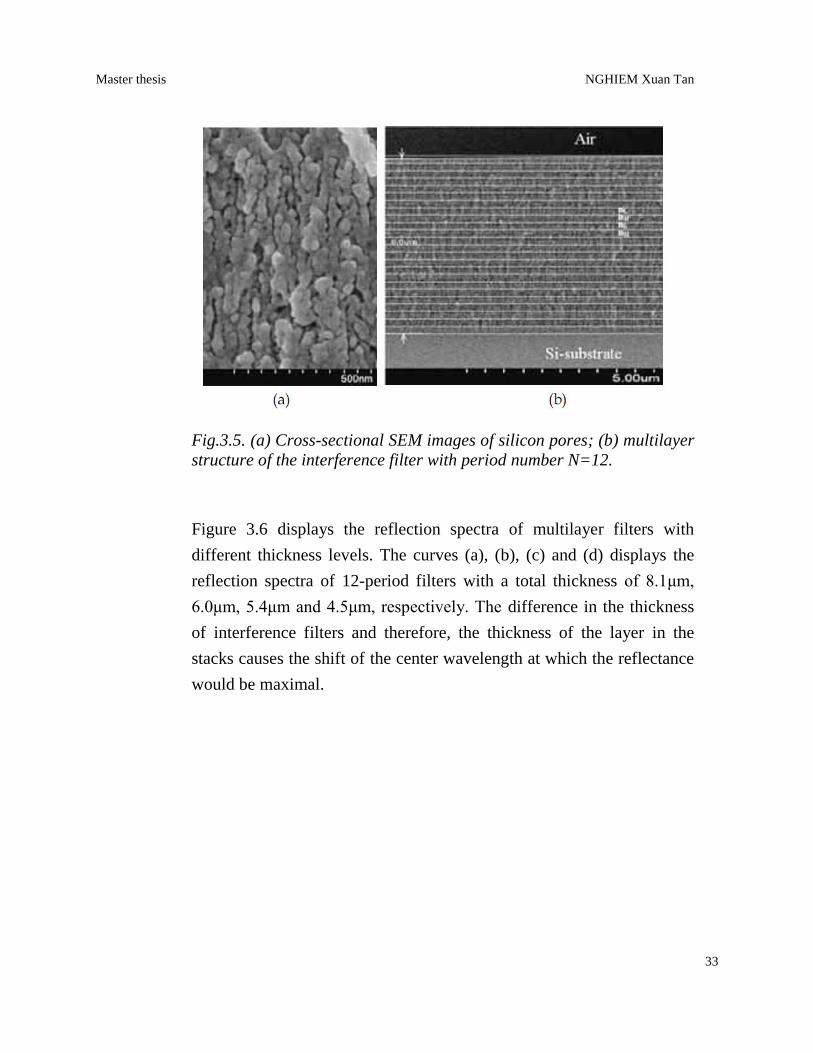
Emission Scanning Electron Microscopy (FE-SEM). Figure 3.5 shows a
FE-SEM-image of the completed porous silicon 12-period compose
fabricated by ratio of current densities J1/J2 = 64/19 and duration time of
6.33 and 12.3 seconds, respectively. As seen in Figure 3.5a, the typical
sizes of the silicon residuals and air voids are about 50nm. This allows
us to describe the PS layers as "an effective medium", whereby its
optical properties mainly depend on its porosity. The SEM-image of the
multilayer displays different gray levels depending on the porosity of
the layers (see Figure 3.5b). Because of this, the layers of the stack are
distinguished and therefore the thickness of each layer can be
experimentally determined.
Fig. 3.4. Schematic of current density modulation versus anodization time
Master thesis NGHIEM Xuan Tan
33
Fig.3.5. (a) Cross-sectional SEM images of silicon pores; (b) multilayer
structure of the interference filter with period number N=12.
Figure 3.6 displays the reflection spectra of multilayer filters with
different thickness levels. The curves (a), (b), (c) and (d) displays the
reflection spectra of 12-period filters with a total thickness of 8.1μm,
6.0μm, 5.4μm and 4.5μm, respectively. The difference in the thickness
of interference filters and therefore, the thickness of the layer in the
stacks causes the shift of the center wavelength at which the reflectance
would be maximal.

Master thesis NGHIEM Xuan Tan
34
Fig. 3.6. Shifting the reflection spectra of 12-period filter by varying the
thickness of the layers in the stacks: (a) h=8.1μm; (b) h=6.0μm; (c)
h=5.4μm; (d) h=4.5μm.
Figure 3.7 shows the reflection spectra from two filters, denoted as M5
and M4, fabricated at a ratio of current densities J1/J2 = 64/19 and 38/19,
respectively. The refractive index of, PS layer depends on anodization
current density, so that the refractive index contract between
neighboring PS layers also depends on the ratio of current densities
which created those layers. The increase in the FWHM (full-width at
half-maximum) of the reflective spectrum from M5 filter compared with
that from M4 one is due to the difference in the ratio of current
densities (J1/J2) forming those filters.

Master thesis NGHIEM Xuan Tan
35
Figure 3.8 shows the reflection spectra at wavelength of 1550 nm-range
from three filters with a different numbers of periods. As seen from this
figure, when period number increases the spectra become shaper,
narrower and the refractivity increased. This result relatively
corresponds to our simulation as shown in Part 2.
The difference in the characteristics of filter spectra from the simulation
and experiment occurs in the filters having too few or too many periods
(N). In the case of filters having too few periods (N≤6), reflection from
the interfaces, especially from the interface between air and the top
layer, becomes more important in those filters, so that the imperfections
of interfaces created by electrochemical etching can cause a deformation
of the reflective spectrum as seen in curve (a) of Figure 3.8.
In the case of the filters having too many periods (N≥18), the long
anodization time causes a deformation of the nano-structure of surface
layers whereas the nano- and micro-structure of the bottom layers can
be affected by the slower transport of etching substances. All of these
factors lead to a break in condition of the Bragg reflection in such layers
and the decrease in reflectivity of the filter as shown in curve (b) of
Figure 3.8.

Master thesis NGHIEM Xuan Tan
36
Fig. 3.7. Reflection spectra versus the refractive index ratio between
nearest layers of PS interference filters.

Master thesis NGHIEM Xuan Tan
37
Fig. 3.8. Reflection spectra versus period numbers of stacks: curves a, b
and c from multilayer filters with periods of 6, 18 and 12, respectively.
The interference filters have a big potential of applications not only for
fiberoptic communication, but for bio-chemical sensory. The Table 3.1
shows an electrochemical etching process for making quarter-wave-
stack filters operated at visible region, which is suitable for bio-
chemical sensors. For making visible-range interference filters, we need
decrease an etching time from tens seconds for IR region to some
seconds for visible, while the current density is kept constantly.

Master thesis NGHIEM Xuan Tan
38
Sample Period numbers Current Density Time (seconds)
Sample No.1 12 J1 = 50 mA.cm-2
2.857
J2 = 15 mA.cm-2
5.555
0 8.0
Sample No.2 12 J1 = 50 mA.cm-2
3.625
J2 = 15 mA.cm-2
6.349
0 8.0
Sample No.3 12 J1 = 50 mA.cm-2
2.653
J2 = 15 mA.cm-2
5.159
0 9.5
Table 3.1 Electrochemical etching process for making interference
filters at visible region
Figure 3.9 shows the reflection spectra of interference filters with
reflection wavelength at 650nm-region, which prepared by etching
process presented in Table 3.1. When the etching time of
electrochemical process increased, the reflection centered wavelength
shifted to red-zone, i.e. the thickness of bi-layer stacks increased.
Fig. 3.9. Reflection spectra of red-light PS filters made by modulation of
current density with different etching time.
Master thesis NGHIEM Xuan Tan
39
We used thermal annealing process of samples for a stabilization of the
optical properties of PS interference filters. The thermal annealing
process of PS samples has three steps:
i) first the PS samples were kept at 60oC for 60 min in air ambient to
stabilize the PS structures;
ii) the pre-oxidation of PS samples was performed at 300oC for different
times varying from 20 to 60 min in oxygen ambient and
iii) keeping the samples in Nitrogen ambient at the same temperature for
30 min and then the temperature decreased with very slow rate to room
temperature.
3.3. Microcavities based on porous silicon layers
Fabry-Perot PS micro-cavity has been formed by electrochemical
etching of high doped p-type silicon wafers (resistivity of 0.01 ÷
0.1Ω.cm) in an aqueous HF: ethanol electrolyte. The p-type silicon
substrates yield the most favorable porous silicon morphology. The
pores are large enough to allow infiltration of other species but
interconnected and small enough to allow porous silicon to be treated as
an optical medium for visible and infrared light. The electrolyte with
concentration 16% HF and ethanol of ratio 1:2, respectively, is chosen
because of the large porosity variation obtained by varying the etching
current.

Master thesis NGHIEM Xuan Tan
40
Description Current Density Etching time (seconds)
DRB on top (4.5 periods) J1 = 15 mA.cm-2
4.762
J2 = 50 mA.cm-2
2.857
Spacer layer (1 period) J3 = 10 mA.cm-2
5.714
DBR on bottom (5 perioda) J1 = 15 mA.cm-2
4.762
J2 = 50 mA.cm-2
2.857
Table 3.2. Electrochemical etching conditions for making PS micro-
cavities
Micro-cavity was formed by periodically varying the applied current
density with two levels (J1 and J2) between 15 and 50mA/cm2 and one
spacer layer (J3). PS micro-cavities are formed by first etching a top
DBR with alternating λ/4-thickness layers of low and high porosities
(high and low refractive indices, respectively), then etching a λ/2-
thickness spacer layer with the designed refractive index, and finally
etching a bottom DBR with the same conditions as the top DBR.
Detailed electrochemical etching conditions are presented in Table 3.2.
The PS micro-cavities used in our cases typically consist of 4.5/5 period
upper/lower DBR. Each period has a pair of low and high porosity
layers. The PS micro-cavity samples have been rinsed in methanol and
isopropanol after anodization process and dried in nitrogen atmosphere.
The micro- and nano-structures of the prepared PS micro-cavity have
been analyzed by using the Scanning Electron Microscopy (FE-SEM
Hitachi S-4800). Figure 3.10 shows the SEM cross-section of a PS
micro-cavity made by electrochemical etching condition shown in table
4. It can be observed in Figure 3.10a that the SEM image shows the
dark and bright layers that have a low and high porosity, respectively.
Based on this difference, the layers of the stack are distinguished and

Master thesis NGHIEM Xuan Tan
41
therefore the thickness of each layer can be determined of about 165
nm. As seen in Figure 3.10b, the typical sizes of the silicon residuals
and air voices are less than 30 nm. The measured reflection spectrum of
PS micro-cavity is shown in Figure 3.11. The spectrum is characterized
by a transmission band at 643.3 nm in between two high reflection
bands. The reflective distinction ratio of 40% and the Full-Width-Half-
Maximum (FWHM) band-pass width of 20 nm were observed in PS
micro-cavity based on symmetrical 5-period DBRs.
Fig. 3.10. SEM cross-section of PS micro-cavity with λ/2-wavelength
thickness spacer for centered wavelength of 650 nm (a) and PS size in
the spacer layer (b).
The preparation of PS structures composed by several layers for DBR
micro–cavity with narrow band-pass width of 2 nm as a design by
simulation is difficult in practice, because the line-width of transmission
of micro-cavity was strongly affected by homogeneity of the layers. The
anodization condition might drift as the sample thickness and refractive
index of stacks, and the solution composition changes with the depth
because of limited exchange through the pores, that caused the different
of experimental results in comparison with simulation one. In general,
the band-pass width of 20 nm at the visible region obtained from the PS

Master thesis NGHIEM Xuan Tan
42
micro-cavity based on electrochemical etching technique is good enable
for applications in the optical sensor, biosensors and/or micro-cavity
lasers.
Fig.3.11. Reflection spectrum of PS micro-cavity with transmission
band of 650nm made by spacer of λ/2- thickness sandwiched between 5-
period DBR.
For a prevention of ageing process of PS layers we used thermal
annealing process of PS samples to obtain SRSO materials. The thermal
annealing process used for SRSO has four steps:
i) first the PS samples were kept at 60oC for 60 min in air ambient to
stabilize the PS structures;
ii) the pre-oxidation of PS samples was performed at 300oC for different
times varying from 20 to 60 min in oxygen ambient;
iii) slowly increasing temperature up to 900oC and keeping samples for
5-10 min in oxygen ambient

Master thesis NGHIEM Xuan Tan
43
iv) keeping the samples in Nitrogen atmosphere at temperature of 900-
1000oC for 30 min and then the temperature was decreased with very
slow rate to room temperature. Table 3.3 presents the shift of
transmission band in the spectra of Fabry-Perot filters based on the as-
prepared and thermally annealed PS micro-cavity at 300oC and 900
oC in
oxygen ambient, respectively.
Sample Centre Wavelength
(nm)
Line-width of
transmission (nm)
Distinction
ratio (%)
as-prepared sample 643.9 22.2 40
300o/40 min 565.6 22.6 34
300o/40 min + 900
oC/5min 472.5 19.2 25
Table 3.3. Shift of narrow transmission band in the spectra of Fabry-
Perot PS filters (the anodization condition was shown in table 3.2)
The 900oC oxidation decreases the centered wavelength of transmission
by more than 170nm and the reflective distinction ratio on 15%, while
the line-width of transmission does not change. This can be explained as
follows: the centered wavelength of transmission corresponds to the
optical thickness of spacer layer that is the product of refractive index
and layer thickness. During the oxidization process at high temperature
the layer thickness and refractive index of spacer decreased, which
causes the shift of transmission wavelength and decrease of reflective
distinction ratio of micro-cavity.
Master thesis NGHIEM Xuan Tan
44
4. CONCLUSION
The thesis work has been presenting the electrochemical process for
making interference filters and DBR micro-cavity based on PS and
SRSO multi-layers with periodical change of refractive indices of the
layer stacks. For the optimal parameters of interference filters and
micro-cavities based on PS and SRSO multi-layers, we use transfer
matrix method for simulation of reflectivity and transmission of
interference filters and DBR micro-cavity with the data obtained from
experiments.
We successfully fabricated the interference filters and DBR micro-
cavity based on porous silicon multilayer which has the selectivity of
wavelength in a range from visible to infra-red range with the
reflectivity of about 90% and transmission line-width of 20nm. The
spectral characteristics of those multi-layers such as desired centered
wavelength (λ0), the FWHM line-width of spectrum, reflectance and
transmission wavelength have been controlled. A good correspondence
between simulation and experimental results has been received.
The imperfection of interfaces of layers created by electrochemical
etching was used to explain a deformation of reflective spectrum from
filters having few periods. The SRSO thin films with single and multi-
layer structures produced by electrochemical method have a big
potential for applications in the active waveguide, optical filter,
chemical and biosensors, DBR micro-cavity lasers.
Master thesis NGHIEM Xuan Tan
45
APPENDIX A: CODE OF PROGRAMME
% This m-file demonstrates phase properties of 1D photonics crystal
% Define input parameters:
clear;
incident_angle = 0;
wl = 400:1:2000; % wl: vector, wavelength range from 400:2000 (nm)
m = size (wl,2);
for q = 1:m
clear wave_length
wave_length = wl(q); % Calcualate for each wavelength as wl(q) changing
% Read the refractive index data from file SiO2_750.txt:
fid=fopen('SiO2_750.txt', 'r'); % open the file
data=fscanf(fid, '%g %g %g',[3 inf]); % read in data
fclose(fid); % close the file
wl_data = data(1, :) ;
n_SiO2_data = data(2, :); % Real part
n_SiO2_data_imag = data(3, :); % Imaginery part
s1 = size(data, 2);
for i=1:s1;
if ((wl_data(i)) == wave_length)
n_SiO2 = n_SiO2_data(i) + + j*n_SiO2_data_imag(i); % Complex refractive index
break;
end
end
% Read the refracetive index data from file Ta.txt:
fid=fopen('Ta2O5_750.txt', 'r'); % open the file
data=fscanf(fid, '%g %g %g',[3 inf]); % read in data
fclose(fid); % close the file
wl_data = data(1, :) ;
n_Ta_data = data(2, :); % Real part
n_Ta_data_imag = data(3, :); % Imaginary part
s2 = size(data, 2);
for i=1:s2
if ((wl_data(i)) == wave_length)
n_Ta = n_Ta_data(i) + j*n_Ta_data_imag(i); % Complex refractive index
break;
end
end
%read the data from file data.txt:
fid=fopen('GDDM1.txt', 'r'); % open the file
data3=fscanf(fid, '%g %c',[2 inf]); % read in data
fclose(fid); % close the file
e = data3(1, :) ;
mat = data3(2, :);
p = size(data3 ,2);
% Deduce refractive indexes from materials and wavelengths
for i= 1:p
if (char(mat(i)) == 'L')
n(i) = n_SiO2 ;
elseif (char(mat(i)) == 'H')
n(i) = n_Ta ;
else
n(i) = 1.52 ; % *** For Substrate

Master thesis NGHIEM Xuan Tan
46
end
end;
% Calculation
clear sigma n01 n02 k a d n1 n2 G y1 y2 i
sigma = 2*pi* sin(incident_angle*pi/180)/wave_length; % scalar
n01 = cos(incident_angle*pi/180) ; % for TE
%n02 = 1/cos(incident_angle*pi/180); % for TM
k = 2*pi*n/wave_length ; % k-vector
a = sqrt(k .^2 - sigma ^2); % coefficient
d = e .* a ; % phrase
n1 = n .* a ./ k ; % for TE
%n2 = n .* k ./a ; % for TM
%
i = p;
y1(p)= n1(p); % for TE
%y2(p)= n2(p) ; % for TM
G = 1;
while (i>1)
y1(i-1) =(-j* n1(i-1)*sin(d(i-1)) + y1(1,i)*cos(d(i-1)))/(cos(d(i-1)) -
j*y1(i)*sin(d(i-1))/n1(i-1));
%y2(i-1) =(-j* n1(i-1)*sin(d(1,i-1)) + y2(1,i)*cos(d(i-1)))/(cos(d(i-1)) -
j*y2(i)*sin(d(i-1))/n1(i-1));
G = G * (cos(d(i-1)) - j*y1(i)*sin(d(i-1))/n1(i-1));
i = i - 1;
end;
r1(q) = ((n01 - y1(1)) / (n01 + y1(1))); % For TE reflectance
R1(q) = r1(q) * r1(q)';
% % r2 = (n02 - y2(1)) / (n02 + y2(1))
% % R2 = r2 * r2' % For TM reflectance
t(q) = (1 + r1(q))/G ; % For TE & TM transmittance
T(q) = real(n1(p))* abs(t(q))^2 / n01;
% Total(q) = T(q) + R1(q); % Check T + R = 1
pr(q) = angle(r1(q)) ; % Phase shift of reflection
pt(q) = angle (t(q)) ; % Phase shift of transmission
end
% This is the graphs show the dependence of Reflection and Transmission on
% wavelengh
pt_uw = unwrap(pt);
pr_uw = unwrap(pr);
subplot (2,4,1)
plot (wl , R1 ,'red');
title('Plot of Reflectance')
xlabel('Wavelengh (nm)');
ylabel ('Reflectance')
refresh
subplot (2,4,2)
plot (wl , T);
title('Plot of Transmittance')
xlabel('Wavelengh (nm)');
ylabel ('Transmittance')
subplot (2,4,3)
plot (wl , pr, 'red');
title('Plot of reflection phase');
xlabel('Wavelengh (nm)');
ylabel ('Reflection phase');
subplot (2,4,4)
plot (wl , pt);
title('Plot of transmition phase');
xlabel('Wavelengh (nm)');
ylabel ('Transmition phase');

Master thesis NGHIEM Xuan Tan
47
% Unwapped the phase and calculate the group dispersion
% gd_r = - diff(pt_uw)./diff(wl).* wl(2:end)* 1.0e-06 /(2*pi* 3.8 * 1.0e+008);
omega = (2*pi* 3 * 1.0e+008) ./ (wl * 1.0e-009) ;
gd_r = diff(pr_uw)./diff(omega); % Group Delay
gdd_r = diff(gd_r) ./ diff(omega(2:end)); % Group Delay Dispersion
gd_t = diff(pt_uw)./diff(omega); % Group Delay
gdd_t = diff(gd_t) ./ diff(omega(2:end)); % Group Delay Dispersion
subplot (2,4,5)
plot (wl(2:end), gd_r, 'red');
title('Plot of reflection GD');
xlabel('Wavelengh (nm)');
ylabel ('Group Delay (s)');
subplot (2,4,6)
plot (wl(2:end), gd_t);
title('Plot of transmition GD');
xlabel('Wavelengh (nm)');
% ylabel ('First Derivative');
subplot (2,4,7)
plot (wl(3:end), gdd_r, 'red');
title('Plot of reflection GDD');
xlabel('Wavelengh (nm)');
% ylabel ('Second Derivative')
subplot (2,4,8)
plot (wl(3:end), gdd_t);
title('Plot of transmition GDD');
xlabel('Wavelengh (nm)');
% ylabel ('Second Derivative');

Master thesis NGHIEM Xuan Tan
48
APPENDIX B: DATA FILES FOR SIMULATION
1) Sample of file of refractive index depend on the wavelength (not consider the imaginary part
of refractive index)
Wavelength(nm) Refractive index 600 2.144718713
601 2.144494571 602 2.144271876 603 2.144050618 604 2.143830783 605 2.14361236 606 2.143395337 607 2.143179701 608 2.142965441 609 2.142752546 610 2.142541004
2) Sample of thickness of the layers for simulation:
Thickness at quarter wavelength (nm)
of layers (H: High reflective index, L: Low reflective index
layer)
63.717 H 93.346 L 63.717 H 93.346 L 63.717 H 93.346 L 63.717 H 93.346 L 63.717 H 93.346 L 63.717 H

Master thesis NGHIEM Xuan Tan
49
References:
[1] J. D. Joannopoulos, S. G. Johnson, J. N. Winn, & R. D. Meade, Photonic Crystals:
Molding the Flow of Light, Princeton University Press (2008).
[2] Wikipedia, Photonic, http://en.wikipedia.org/wiki/Photonics
[3] Tesis Galisteo, PhD thesis: AN OPTICAL STUDY OF OPAL BASED PHOTONIC
CRYSTALS, Universidad Autónoma de Madrid (2005).
[4] Wikipedia, Porous Silicon http://en.wikipedia.org/wiki/Porous_silicon
[5] R.C. Anderson, R.S. Muller, and C.W. Tobias, Investigations of Porous Si for Vapor
Sensing, Sens. Actuators A, 21, 835 (1990).
[6] Canham, L.T., Si Quantum Wire Array Fabrication by Electrochemical and
Chemical Dissolution. Appl. Phys. Lett., 57(10): p. 1046-1048 (1990).
[7] Bettotti, P., Cazzanelli, M., Dal Negro, L., Danese, B., Gaburro, Z., Oton, C.J.,
Vijaya Prakash, G., Pavesi, L., Silicon nanostructure for photonics, J. Phys.:
Condens. Matter. 14, 8253- 8281 (2002).
[8] Shin, J. H., van d’Hoven, G. N., Polman, A., Origin of the 1.54μm luminescence of
Erbium-implanted porous silicon, Appl. Phys.Lett. 66, 2379-2381 (1995).
[9] Kimura, T., Yokoi, A., Horiguchi, H., Saito, R., Ikoma, T., Saito, A.,
Electrochemical Er-doping of porous silicon and its room-temperature luminescence
at 1.54μm, Appl. Phys. Lett. 65, 983-985 (1994)
[10] L.T. Canham, A.G. Cullis, C. Pickering, O.D. Dosserm, T.I. Cox, T.P. Lynch,
Luminescent anodized silicon aerocrystal networks prepared by supercritical drying
Nature, 368, 133 (1994).
[11] C. Mazzoleni and L. Pavesi., Application to optical components of dielectric porous
silicon multilayers Appl. Phys. Lett., 67, 2983 (1995). (tên bài báo)
[12] V. Agarwal, and J.A. del Río, Tailoring the photonic band gap of a porous silicon
dielectric mirror Appl. Phys. Lett., 82, 1512 (2003).
[13] S. Setzu, P. Ferrand, and R. Romestain, Optical properties of multilayered porous
silicon, Mat. Sci. and Eng. B, 69, 34 (2000).
[14] M.G. Berger, C. Dieker, M. Thönissen, L. Vescan, H. Lüth, H. Munder, W. Theiss,
M. Wernke, and P. Grosse, Porosity superlattices: a new class of Si heterostructures
J. Phys. D, 27, 1333 (1994).
[15] L. Pavesi, Porous silicon dielectric multilayers and microcavities, Riv. del Nuovo
Cimento, 20, 18 (1997).

Master thesis NGHIEM Xuan Tan
50
[16] S. Chan, P.M. Fauchet, Tunable, Narrow, And Directional Luminescence From
Porous Silicon Light Emitting Devices, Appl. Phys Lett., 75, 274, (1999).
[17] J.E. Lugo, H.A. Lópz, S. Cahn, P.M. Fauchet, Porous silicon multilayer structures: A
photonic band gap analysis, J. Appl. Phys., 91, 4966 (2002).
[18] E.K. Squire, P.A. Snow, and P.St. Russell, Light Emission from Highly Reflective
Porous Silicon Multilayer Structures, J. Porous Materials, 7, 209 (2000).
[19] S. Setzu, G. Lérondel, R. Romestain, Temperature effect on the roughness of the
formation interface of p-type porous silicon, J. Appl. Phys., 84, 3129 (1998).
[20] G. Vincent, Optical properties of porous silicon superlattices, Appl. Phys. Lett., 64,
2367 (1994).
[21] J. Diener, N. Künzner, D. Kovalev, E. Gross, V.Y. Timoshenko, G. Polisski, and
F.Koch, Planar silicon-based light polarizers, Appl. Phys. Lett., 78, 3887 (2001).
[22] A. Szerling, D. Wawer, K. Hejduk, T. Piwonski, A. Wojcik, B. Mroziewicz, and M.
Bugajski, Reflectance study of SiO2/Si3N4 dielectric Bragg reflectors, Optica
Applicata, 32, 523 (2002).
[23] C.P. Hussell, and R.V. Ramaswamy, High-index overlay for high-reflectance DBR
gratings in LiNbO3 channel waveguides, IEEE Photonics Technology Letters, 9, 636
(1997).
[24] L. Pavesi, Brillouin scattering from porous silicon-based optical Bragg mirrors, Riv.
del Nuovo Cimento, 10, 1 (1997).
[25] A. Loni, L.T. Canham, M.G. Berger, R. Arens-Fischer, H. Munder, H. Luth, H.F.
Arrand, and T.M. Benson, Porous silicon multilayer optical waveguides, Thin Solid
Films, 276, 143 (1996).
[26] S.M. Weiss, and P.M. Fauchet, Electrically tunable porous silicon active mirrors,
Phys. Stat. Sol (a), 2, 556 (2003).
[27] T. Gao, J. Gao, M.J. Sailor, Langmuir, Tuning the response and stability of thin film
mesoporous silicon vapor sensors by surface modification, 18, 9953 (2002).
[28] L. De Stefano, I. Rendina, L. Moretti, and A.M. Rossi, Photonic Crystal Sensors
Based on Porous Silicon, Mater. Sci. and Eng.B., 100, 271 (2003).
[29] J. Volk, J. Balazs, A.L. Tóth, and I. Bársony, Porous Silicon Multilayers for Sensing
by Tuneable IR-Trans mission Filtering, Sens. Actuators B, 100, 163 (2004).
[30] M.A. Anderson, A.Tinsley-Bown, P. Allcock, E.A. Perkins, P. Snow, M. Hollings,
R.G. Smith, C. Reeves, D.J. Squirrell, S. Nicklin, and T.I. Cox, Sensitivity of the
optical properties of porous silicon layers to the refractive index of liquid in the
pores, Phys. Stat. Sol. (a), 197, 528 (2003).

Master thesis NGHIEM Xuan Tan
51
[31] P.J. Reece, G. Lérondel, W.H. Zheng, and M. Gal, Optical microcavities with
subnanometer linewidths based on porous silicon, Appl. Phys. Lett., 81, 4895 (2002).
[32] Y.Y. Kim, K.W. Lee, C.W. Lee, S. Hong, J.W. Ryu and J.H. Jeon, J. Korean Phys.
Soc., 42, 329 (2003).
[33] T.V. Dolgova, A.I. Maidykovski, M.G. Martemyanov, A.A. Fedyanin, O.A.
Aktsipetrov, G. Marowsky, V.A. Yakovlev, and G. Mattei, Giant microcavity
enhancement of second-harmonic generation in all-silicon photonic crystals, Appl.
Phys. Lett., 81, 2725 (2002).
[34] M.G. Martemyanov, E.M. Kim, T.V. Dolgova, A.A. Fedyanin, O.A. Aktsipetrov, and
G. Marowsky, Third-harmonic generation in silicon photonic crystals and
microcavities, Phys. Rev. B, 70, 073311 (2004).
[35] Smith, R.L., Collins, S.D., Porous silicon formation mechanism, J. Appl.Phys.
71(8), R1 (21 pages) (1992).
[36] Valance, A., Theoretical model for early stages of porous silicon formation
from n- and p-type silicon substrates, Phys. Rev. B 55, 9706-9715 (1997).
[37] Lehmann, V., Gösele, U., Porous silicon formation – a quantum wire effect,
Apll. Phys. Lett. 58, 856-858 (1991).
[38] Bui, H., Pham, V.H., Phan , H.K., Nguyen, T.V., and Do, T.C., Porous silicon as a
promising material for photonics, Int. J. Nanotechnol. 8, 360-370 (2011)
[39] Pham, V.H., Do, T.C., Bui, H., Nguyen, T.V., Silicon-rich silicon oxide thin film
fabricated by electro-chemical method, Chapter 2 in Optoelectronics – Materials and
Techniques, P. Predeep, ed., Publisher InTech, Rijeka Croatia (2011)
[40] J. Charrier, M. Guendouz, L. Haji, and P. Joubert, Porosity Gradient Resulting from
Localised Formation of Porous Silicon: The Effect on Waveguiding, Phys. Stat. Sol.
(a),182, 431 (2000).
[41] E.K. Squire, P.A. Snow, P.St. Russell, L.T. Canham, A.J. Simons, and C.L. Reeves,
Light emission from porous silicon single and multiple cavities J. Luminescence, 80,
125 (1999).
[42] H. S. Nalwa, Silicon Based Materials and Devices, Vol. 2: Properties and Devices,
Academic Press, San Diego (2001).
[43] V. Agarwal, and J.A. del Río, Tailoring the photonic band gap of a porous silicon
dielectric mirror, Appl. Phys. Lett., 82, 1512 (2003).
[44] E. Lorenzo, C.J. Oton, B.J. González Díaz, C. Hernández Rodríguez, R. Guerrero
Lemus, and N.E. Capuj, Fabrication and optimization of rugate filters based on
porous silicon, phys. stat. sol. (c), 2, 3227 (2005).