Embed Size (px)
Citation preview
NI UltiboardTM
Fundamentals
NI Ultiboard Fundamentals
January 2012373180B-01
Support
Worldwide Technical Support and Product Information
ni.com
Worldwide Offices
Visit ni.com/niglobal to access the branch office Web sites, which provide up-to-date contact information, support phone numbers, email addresses, and current events.
National Instruments Corporate Headquarters
11500 North Mopac Expressway Austin, Texas 78759-3504 USA Tel: 512 683 0100
For further support information, refer to the Technical Support and Professional Services appendix. To comment on National Instruments documentation, refer to the National Instruments Web site at ni.com/info and enter the Info Code feedback.
© 2006–2012 National Instruments Corporation. All rights reserved.
Important Information
WarrantyThe media on which you receive National Instruments software are warranted not to fail to execute programming instructions, due to defects in materials and workmanship, for a period of 90 days from date of shipment, as evidenced by receipts or other documentation. National Instruments will, at its option, repair or replace software media that do not execute programming instructions if National Instruments receives notice of such defects during the warranty period. National Instruments does not warrant that the operation of the software shall be uninterrupted or error free.
A Return Material Authorization (RMA) number must be obtained from the factory and clearly marked on the outside of the package before any equipment will be accepted for warranty work. National Instruments will pay the shipping costs of returning to the owner parts which are covered by warranty.
National Instruments believes that the information in this document is accurate. The document has been carefully reviewed for technical accuracy. In the event that technical or typographical errors exist, National Instruments reserves the right to make changes to subsequent editions of this document without prior notice to holders of this edition. The reader should consult National Instruments if errors are suspected. In no event shall National Instruments be liable for any damages arising out of or related to this document or the information contained in it.
EXCEPT AS SPECIFIED HEREIN, NATIONAL INSTRUMENTS MAKES NO WARRANTIES, EXPRESS OR IMPLIED, AND SPECIFICALLY DISCLAIMS ANY WARRANTY OF MERCHANTABILITY OR FITNESS FOR A PARTICULAR PURPOSE. CUSTOMER’S RIGHT TO RECOVER DAMAGES CAUSED BY FAULT OR NEGLIGENCE ON THE PART OF NATIONAL INSTRUMENTS SHALL BE LIMITED TO THE AMOUNT THERETOFORE PAID BY THE CUSTOMER. NATIONAL INSTRUMENTS WILL NOT BE LIABLE FOR DAMAGES RESULTING FROM LOSS OF DATA, PROFITS, USE OF PRODUCTS, OR INCIDENTAL OR CONSEQUENTIAL DAMAGES, EVEN IF ADVISED OF THE POSSIBILITY THEREOF. This limitation of the liability of National Instruments will apply regardless of the form of action, whether in contract or tort, including negligence. Any action against National Instruments must be brought within one year after the cause of action accrues. National Instruments shall not be liable for any delay in performance due to causes beyond its reasonable control. The warranty provided herein does not cover damages, defects, malfunctions, or service failures caused by owner’s failure to follow the National Instruments installation, operation, or maintenance instructions; owner’s modification of the product; owner’s abuse, misuse, or negligent acts; and power failure or surges, fire, flood, accident, actions of third parties, or other events outside reasonable control.
CopyrightUnder the copyright laws, this publication may not be reproduced or transmitted in any form, electronic or mechanical, including photocopying, recording, storing in an information retrieval system, or translating, in whole or in part, without the prior written consent of National Instruments Corporation.
National Instruments respects the intellectual property of others, and we ask our users to do the same. NI software is protected by copyright and other intellectual property laws. Where NI software may be used to reproduce software or other materials belonging to others, you may use NI software only to reproduce materials that you may reproduce in accordance with the terms of any applicable license or other legal restriction.
Anti-Grain Geometry - Version 2.4
Copyright (C) 2002-2004 Maxim Shemanarev (McSeem)
Permission to copy, use, modify, sell and distribute this software is granted provided this copyright notice appears in all copies. This software is provided “as is” without express or implied warranty, and with no claim as to its suitability for any purpose.
Anti-Grain Geometry - Version 2.4
Copyright (C) 2002-2005 Maxim Shemanarev (McSeem)
1. Redistribution and use in source and binary forms, with or without modification, are permitted provided that the following conditions are met:
2. Redistributions of source code must retain the above copyright notice, this list of conditions and the following disclaimer.
3. Redistributions in binary form must reproduce the above copyright notice, this list of conditions and the following disclaimer in the documentation and/or other materials provided with the distribution.
The name of the author may not be used to endorse or promote products derived from this software without specific prior written permission.
THIS SOFTWARE IS PROVIDED BY THE AUTHOR “AS IS” AND ANY EXPRESS OR IMPLIED WARRANTIES, INCLUDING, BUT NOT LIMITED TO, THE IMPLIED WARRANTIES OF MERCHANTABILITY AND FITNESS FOR A PARTICULAR PURPOSE ARE DISCLAIMED. IN NO EVENT SHALL THE AUTHOR BE LIABLE FOR ANY DIRECT, INDIRECT, INCIDENTAL, SPECIAL, EXEMPLARY, OR CONSEQUENTIAL DAMAGES (INCLUDING, BUT NOT LIMITED TO, PROCUREMENT OF SUBSTITUTE GOODS OR SERVICES; LOSS OF USE, DATA, OR PROFITS; OR BUSINESS INTERRUPTION) HOWEVER CAUSED AND ON ANY THEORY OF LIABILITY, WHETHER IN CONTRACT, STRICT LIABILITY, OR TORT (INCLUDING NEGLIGENCE OR OTHERWISE) ARISING IN ANY WAY OUT OF THE USE OF THIS SOFTWARE, EVEN IF ADVISED OF THE POSSIBILITY OF SUCH DAMAGE.
TrademarksLabVIEW, National Instruments, NI, ni.com, the National Instruments corporate logo, and the Eagle logo are trademarks of National Instruments Corporation. Refer to the Trademark Information at ni.com/trademarks for other National Instruments trademarks.
Electronics Workbench, Multisim and Ultiboard are trademarks of National Instruments.
Portions of this product obtained under license from Bartels Systems GmbH.
Other product and company names mentioned herein are trademarks or trade names of their respective companies.
Members of the National Instruments Alliance Partner Program are business entities independent from National Instruments and have no agency, partnership, or joint-venture relationship with National Instruments.
PatentsFor patents covering National Instruments products/technology, refer to the appropriate location: Help»Patents in your software, the patents.txt file on your media, or the National Instruments Patent Notice at ni.com/patents.

Export Compliance InformationRefer to the Export Compliance Information at ni.com/legal/export-compliance for the National Instruments global trade compliance policy and how to obtain relevant HTS codes, ECCNs, and other import/export data.
WARNING REGARDING USE OF NATIONAL INSTRUMENTS PRODUCTS(1) NATIONAL INSTRUMENTS PRODUCTS ARE NOT DESIGNED WITH COMPONENTS AND TESTING FOR A LEVEL OF RELIABILITY SUITABLE FOR USE IN OR IN CONNECTION WITH SURGICAL IMPLANTS OR AS CRITICAL COMPONENTS IN ANY LIFE SUPPORT SYSTEMS WHOSE FAILURE TO PERFORM CAN REASONABLY BE EXPECTED TO CAUSE SIGNIFICANT INJURY TO A HUMAN.
(2) IN ANY APPLICATION, INCLUDING THE ABOVE, RELIABILITY OF OPERATION OF THE SOFTWARE PRODUCTS CAN BE IMPAIRED BY ADVERSE FACTORS, INCLUDING BUT NOT LIMITED TO FLUCTUATIONS IN ELECTRICAL POWER SUPPLY, COMPUTER HARDWARE MALFUNCTIONS, COMPUTER OPERATING SYSTEM SOFTWARE FITNESS, FITNESS OF COMPILERS AND DEVELOPMENT SOFTWARE USED TO DEVELOP AN APPLICATION, INSTALLATION ERRORS, SOFTWARE AND HARDWARE COMPATIBILITY PROBLEMS, MALFUNCTIONS OR FAILURES OF ELECTRONIC MONITORING OR CONTROL DEVICES, TRANSIENT FAILURES OF ELECTRONIC SYSTEMS (HARDWARE AND/OR SOFTWARE), UNANTICIPATED USES OR MISUSES, OR ERRORS ON THE PART OF THE USER OR APPLICATIONS DESIGNER (ADVERSE FACTORS SUCH AS THESE ARE HEREAFTER COLLECTIVELY TERMED “SYSTEM FAILURES”). ANY APPLICATION WHERE A SYSTEM FAILURE WOULD CREATE A RISK OF HARM TO PROPERTY OR PERSONS (INCLUDING THE RISK OF BODILY INJURY AND DEATH) SHOULD NOT BE RELIANT SOLELY UPON ONE FORM OF ELECTRONIC SYSTEM DUE TO THE RISK OF SYSTEM FAILURE. TO AVOID DAMAGE, INJURY, OR DEATH, THE USER OR APPLICATION DESIGNER MUST TAKE REASONABLY PRUDENT STEPS TO PROTECT AGAINST SYSTEM FAILURES, INCLUDING BUT NOT LIMITED TO BACK-UP OR SHUT DOWN MECHANISMS. BECAUSE EACH END-USER SYSTEM IS CUSTOMIZED AND DIFFERS FROM NATIONAL INSTRUMENTS' TESTING PLATFORMS AND BECAUSE A USER OR APPLICATION DESIGNER MAY USE NATIONAL INSTRUMENTS PRODUCTS IN COMBINATION WITH OTHER PRODUCTS IN A MANNER NOT EVALUATED OR CONTEMPLATED BY NATIONAL INSTRUMENTS, THE USER OR APPLICATION DESIGNER IS ULTIMATELY RESPONSIBLE FOR VERIFYING AND VALIDATING THE SUITABILITY OF NATIONAL INSTRUMENTS PRODUCTS WHENEVER NATIONAL INSTRUMENTS PRODUCTS ARE INCORPORATED IN A SYSTEM OR APPLICATION, INCLUDING, WITHOUT LIMITATION, THE APPROPRIATE DESIGN, PROCESS AND SAFETY LEVEL OF SUCH SYSTEM OR APPLICATION.
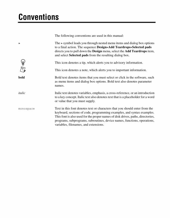
Conventions
The following conventions are used in this manual:
» The » symbol leads you through nested menu items and dialog box options to a final action. The sequence Design»Add Teardrops»Selected pads directs you to pull down the Design menu, select the Add Teardrops item, and select Selected pads from the resulting dialog box.
This icon denotes a tip, which alerts you to advisory information.
This icon denotes a note, which alerts you to important information.
bold Bold text denotes items that you must select or click in the software, such as menu items and dialog box options. Bold text also denotes parameter names.
italic Italic text denotes variables, emphasis, a cross-reference, or an introduction to a key concept. Italic text also denotes text that is a placeholder for a word or value that you must supply.
monospace Text in this font denotes text or characters that you should enter from the keyboard, sections of code, programming examples, and syntax examples. This font is also used for the proper names of disk drives, paths, directories, programs, subprograms, subroutines, device names, functions, operations, variables, filenames, and extensions.
© National Instruments Corporation vii NI Ultiboard Fundamentals
Contents
Chapter 1Introduction
Chapter 2User Interface
Introduction....................................................................................................................2-2Toolbars .........................................................................................................................2-3Setting Layout Preferences ............................................................................................2-3Spreadsheet View ..........................................................................................................2-4Design Toolbox..............................................................................................................2-5Birds Eye View..............................................................................................................2-6Customizing the Interface ..............................................................................................2-6
Chapter 3Setting Up a Design
Designs and Projects ......................................................................................................3-1Technology Files............................................................................................................3-2Working with Layers .....................................................................................................3-2Working with the Board Outline ...................................................................................3-3Working with the Group Editor .....................................................................................3-3
Chapter 4Working with Parts
Placing Parts ..................................................................................................................4-1Editing Properties ..........................................................................................................4-3Swapping Pins and Gates...............................................................................................4-3Searching For and Replacing Parts ................................................................................4-4Working with the Database............................................................................................4-4
Chapter 5Working with Nets and Copper
Nets ................................................................................................................................5-1Traces and Vias..............................................................................................................5-3Copper............................................................................................................................5-4Other Elements ..............................................................................................................5-4PCB Calculators.............................................................................................................5-5
Contents
NI Ultiboard Fundamentals viii ni.com
Chapter 6Autoplacement and Autorouting
Autoplacement............................................................................................................... 6-1Autorouting.................................................................................................................... 6-2
Chapter 7Working with Schematic Capture
Creating a Design from a Netlist File............................................................................ 7-1Forward and Backward Annotation............................................................................... 7-1Cross-Probing ................................................................................................................ 7-2
Chapter 8Preparing for Manufacturing/Assembly
Design Rule Errors ........................................................................................................ 8-1Cleaning up the Board ................................................................................................... 8-2Documenting Your Design............................................................................................ 8-3Viewing the Board in 3D............................................................................................... 8-4
Internal View................................................................................................... 8-4Mechanical CAD........................................................................................................... 8-5Viewing Gerber Files .................................................................................................... 8-5Exporting a File ............................................................................................................ 8-6
Appendix ATechnical Support and Professional Services
Index
© National Instruments Corporation 1-1 NI Ultiboard Fundamentals
1Introduction
National Instruments Circuit Design Suite is a suite of EDA (Electronics Design Automation) tools that assist you in carrying out the major steps in the circuit design flow.
Ultiboard is used to design printed circuit boards, perform certain basic mechanical CAD operations, and prepare them for manufacturing. It also provides automated parts placement and layout.
This manual describes some of the basic features of Ultiboard.
Some of the described features may not be available in your edition of Ultiboard. Refer to the NI Circuit Design Suite Release Notes for a list of the features available in your edition.
Refer to Getting Started with NI Circuit Design Suite for an introductory tutorial on how to use Ultiboard.
Refer to the Ultiboard Help for complete information on the features described in this manual.
© National Instruments Corporation 2-1 NI Ultiboard Fundamentals
2User Interface
This chapter introduces you to Ultiboard’s user interface.
Some of the described features may not be available in your edition of Ultiboard. Refer to the NI Circuit Design Suite Release Notes for a list of the features in your edition.
Refer to the Ultiboard Help for complete information on the features found in this chapter.
Chapter 2 User Interface
NI Ultiboard Fundamentals 2-2 ni.com
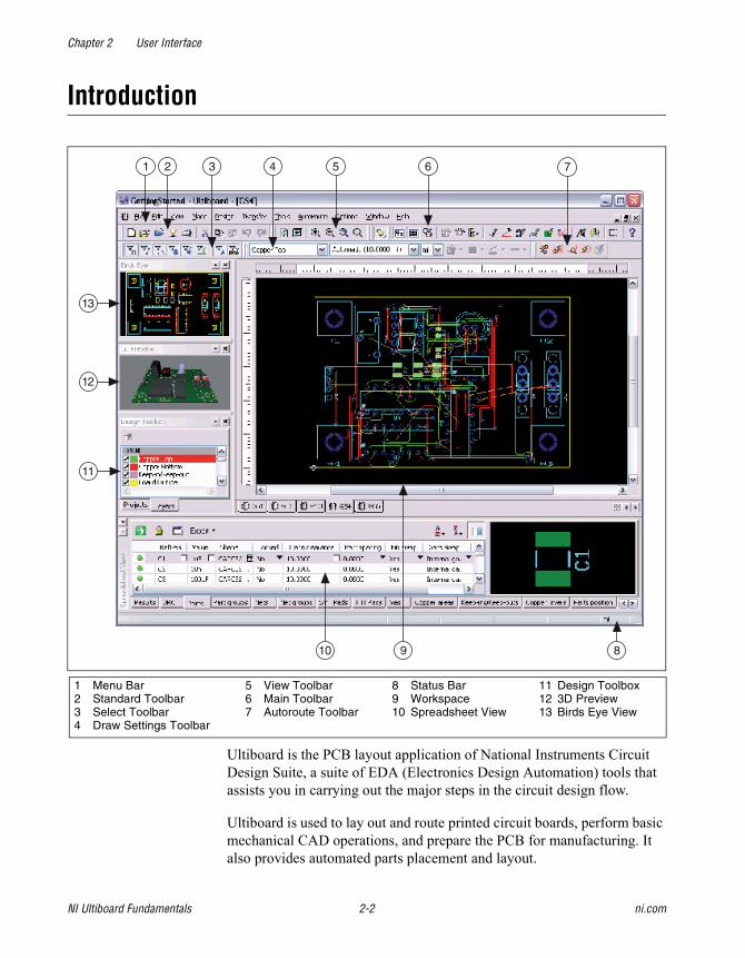
Introduction
Ultiboard is the PCB layout application of National Instruments Circuit Design Suite, a suite of EDA (Electronics Design Automation) tools that assists you in carrying out the major steps in the circuit design flow.
Ultiboard is used to lay out and route printed circuit boards, perform basic mechanical CAD operations, and prepare the PCB for manufacturing. It also provides automated parts placement and layout.
1 Menu Bar2 Standard Toolbar3 Select Toolbar4 Draw Settings Toolbar
5 View Toolbar6 Main Toolbar7 Autoroute Toolbar
8 Status Bar9 Workspace10 Spreadsheet View
11 Design Toolbox12 3D Preview13 Birds Eye View
1
13
12
11
10 9 8
2 3 4 5 6 7
Chapter 2 User Interface
© National Instruments Corporation 2-3 NI Ultiboard Fundamentals
Note For detailed information about the Ultiboard interface, and information on the other components of NI Circuit Design Suite, refer to the Ultiboard Help and the Getting Started with NI Circuit Design Suite manual.
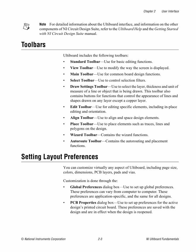
Toolbars Ultiboard includes the following toolbars:
• Standard Toolbar—Use for basic editing functions.
• View Toolbar—Use to modify the way the screen is displayed.
• Main Toolbar—Use for common board design functions.
• Select Toolbar—Use to control selection filters.
• Draw Settings Toolbar—Use to select the layer, thickness and unit of measure of a line or object that is being drawn. This toolbar also contains buttons for functions that control the appearance of lines and shapes drawn on any layer except a copper layer.
• Edit Toolbar—Use for editing specific elements, including in-place editing and orientation.
• Align Toolbar—Use to align and space design elements.
• Place Toolbar—Use to place elements such as traces, lines and polygons on the design.
• Wizard Toolbar—Contains the wizard functions.
• Autoroute Toolbar—Contains the autorouting and placement functions.
Setting Layout Preferences You can customize virtually any aspect of Ultiboard, including page size, colors, dimensions, PCB layers, pads and vias.
Customization is done through the:
• Global Preferences dialog box—Use to set up global preferences. These preferences can vary from computer to computer. These preferences are application-specific, and the same for all designs.
• PCB Properties dialog box—Use to set up preferences for the active design’s printed circuit board. These preferences are saved with the design and are in effect when the design is reopened.
Chapter 2 User Interface
NI Ultiboard Fundamentals 2-4 ni.com
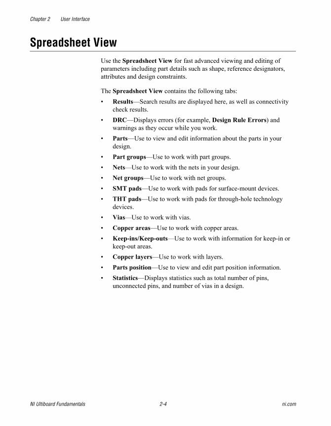
Spreadsheet View Use the Spreadsheet View for fast advanced viewing and editing of parameters including part details such as shape, reference designators, attributes and design constraints.
The Spreadsheet View contains the following tabs:
• Results—Search results are displayed here, as well as connectivity check results.
• DRC—Displays errors (for example, Design Rule Errors) and warnings as they occur while you work.
• Parts—Use to view and edit information about the parts in your design.
• Part groups—Use to work with part groups.
• Nets—Use to work with the nets in your design.
• Net groups—Use to work with net groups.
• SMT pads—Use to work with pads for surface-mount devices.
• THT pads—Use to work with pads for through-hole technology devices.
• Vias—Use to work with vias.
• Copper areas—Use to work with copper areas.
• Keep-ins/Keep-outs—Use to work with information for keep-in or keep-out areas.
• Copper layers—Use to work with layers.
• Parts position—Use to view and edit part position information.
• Statistics—Displays statistics such as total number of pins, unconnected pins, and number of vias in a design.
Chapter 2 User Interface
© National Instruments Corporation 2-5 NI Ultiboard Fundamentals
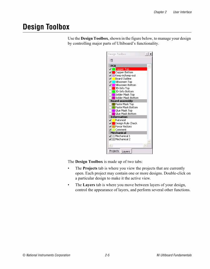
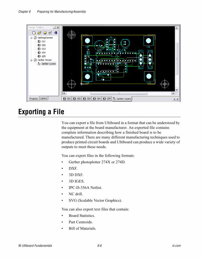
Design Toolbox Use the Design Toolbox, shown in the figure below, to manage your design by controlling major parts of Ultiboard’s functionality.
The Design Toolbox is made up of two tabs:
• The Projects tab is where you view the projects that are currently open. Each project may contain one or more designs. Double-click on a particular design to make it the active view.
• The Layers tab is where you move between layers of your design, control the appearance of layers, and perform several other functions.
Chapter 2 User Interface
NI Ultiboard Fundamentals 2-6 ni.com
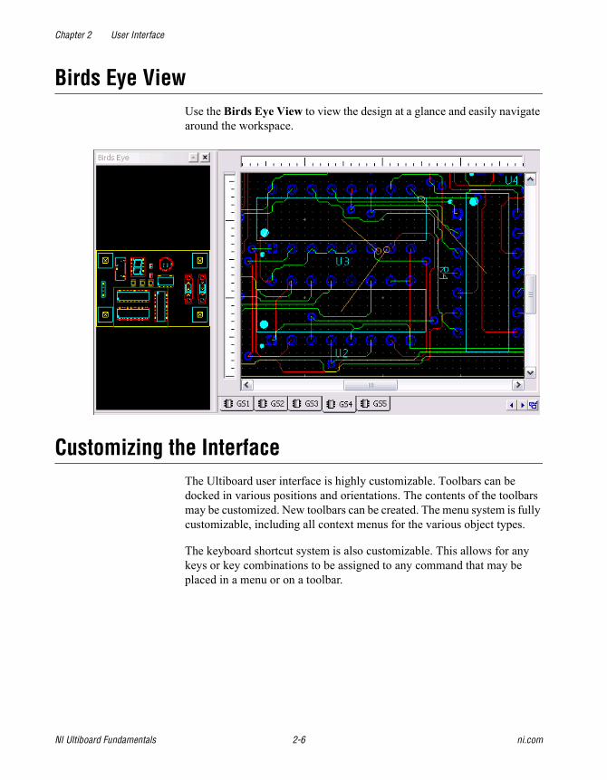
Birds Eye View Use the Birds Eye View to view the design at a glance and easily navigate around the workspace.
Customizing the Interface The Ultiboard user interface is highly customizable. Toolbars can be docked in various positions and orientations. The contents of the toolbars may be customized. New toolbars can be created. The menu system is fully customizable, including all context menus for the various object types.
The keyboard shortcut system is also customizable. This allows for any keys or key combinations to be assigned to any command that may be placed in a menu or on a toolbar.
© National Instruments Corporation 3-1 NI Ultiboard Fundamentals
3Setting Up a Design
This chapter describe some basic features that are useful when setting up a design.
Some of the described features may not be available in your edition of Ultiboard. Refer to the NI Circuit Design Suite Release Notes for a list of the features in your edition.
Refer to the Ultiboard Help for complete information on the features found in this chapter.
Designs and Projects Designs are stored inside projects, allowing you to group them together for easy access. In this way, all designs that have a logical connection between them (that is, they may all relate to a specific project) are conveniently located in one file. In the figure below, Getting Started is the project, and GS1 through GS5 are the designs.
Chapter 3 Setting Up a Design
NI Ultiboard Fundamentals 3-2 ni.com
Technology Files You can save the technology settings, such as design rules, from the current design into a technology file using the Technology File Settings dialog box. This technology file can be used to import technology settings into another design.
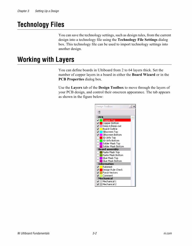
Working with Layers You can define boards in Ultiboard from 2 to 64 layers thick. Set the number of copper layers in a board in either the Board Wizard or in the PCB Properties dialog box.
Use the Layers tab of the Design Toolbox to move through the layers of your PCB design, and control their onscreen appearance. The tab appears as shown in the figure below:
Chapter 3 Setting Up a Design
© National Instruments Corporation 3-3 NI Ultiboard Fundamentals
Working with the Board Outline The Board Outline layer is empty for new designs. You can create a board outline by:
• Drawing a board outline using the drawing tools. For example, choose Place»Graphic»Rectangle to place a rectangular board outline.
• Importing a DXF file from a CAD program.
• Placing a pre-defined outline from the Ultiboard database.
• Using the Board Wizard.
Working with the Group Editor The Group Editor dialog box is where you create and edit:
• Net groups—You can change the parameters of multilple nets at the same time.
• Part groups—You can change the parameters of multiple parts at the same time.
• Bus groups—Set up a bus group for traces that you wish to route as closely together as possible during auto trace routing.
• Differential pairs—A differential pair has two traces that carry signals that are equal in value, but opposite in polarity.
© National Instruments Corporation 4-1 NI Ultiboard Fundamentals
4Working with Parts
This chapter explains some of the basics involved in working with parts in Ultiboard.
Some of the described features may not be available in your edition of Ultiboard. Refer to the NI Circuit Design Suite Release Notes for a list of the features in your edition.
Refer to the Ultiboard Help for complete information on the features found in this chapter.
Placing Parts You can use any of the following methods to place parts on a design:
• Drag them from outside the board outline. This is the most commonly-used method.
• Use the Parts tab in the Spreadsheet View.
• Import a netlist.
• Select parts directly from the Ultiboard database.
• Use the autoplacer.
Ultiboard also has many tools to assist in part placement, including:
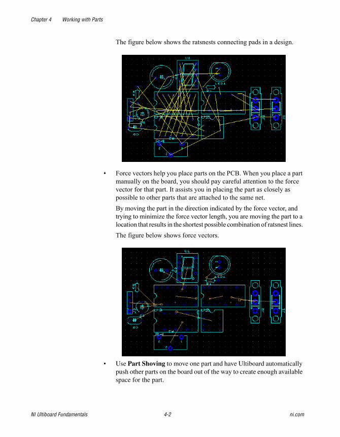
• A ratsnest is a straight line connection between pads, indicating their connectivity. The ratsnest identifies the pads which should be connected according to the netlist, but which are not yet connected with traces. Because these represent logical connections, and not the physical copper connections referred to as traces in Ultiboard, they are just straight line connections that can overlap parts and other ratsnest lines.
Chapter 4 Working with Parts
NI Ultiboard Fundamentals 4-2 ni.com
The figure below shows the ratsnests connecting pads in a design.
• Force vectors help you place parts on the PCB. When you place a part manually on the board, you should pay careful attention to the force vector for that part. It assists you in placing the part as closely as possible to other parts that are attached to the same net.
By moving the part in the direction indicated by the force vector, and trying to minimize the force vector length, you are moving the part to a location that results in the shortest possible combination of ratsnest lines.
The figure below shows force vectors.
• Use Part Shoving to move one part and have Ultiboard automatically push other parts on the board out of the way to create enough available space for the part.
Chapter 4 Working with Parts
© National Instruments Corporation 4-3 NI Ultiboard Fundamentals
Editing Properties You can edit a part from its properties dialog box—select the part and choose Edit»Properties.
The Part Properties dialog box has four tabs:
• Attributes—Parts are generally the only elements that have predefined attributes, typically including a RefDes, a value, and a shape. Attributes can be changed, added, and in some cases, removed.
• Position—Controls the coordinates of the selected part.
• 3D data—Controls the properties of the 3D image of the selected part.
• Part—This is where you adjust the distance of part shove spacing, enter pin and gate swapping settings, and enter trace clearances.
You can also edit other elements in a similar manner, including attributes (for example, a part’s RefDes), through hole and surface mount pins.
Tip Use in-place part editing to add, change or delete a part’s pads and lines, or to place new shapes or lines on it.
Tip You can design your own parts using the Database Manager or the Part Wizard.
Swapping Pins and Gates Pin and gate swapping are done between similar pins and gates to reduce the amount of copper needed to route a given net.
You can swap pins between allowed pins in the same gate (section of an IC). Swapping of pins between gates in the same IC or between similar ICs is not allowed.
Use gate swapping to swap gates for similar gates in the same IC, or for gates in similar ICs.
Tip Use automatic pin/gate swapping to swap pins and/or gates after moving parts on the workspace. Pins and gates are swapped to achieve the most efficient routing of nets possible. You can also set up real time pin/gate swapping in the Spreadsheet View, and enable it in the Design rules tab of the PCB Properties dialog box.
Chapter 4 Working with Parts
NI Ultiboard Fundamentals 4-4 ni.com
Searching For and Replacing Parts To find out if a part exists in any open design, search for it with the Edit»Find command. While this command works much like a Find function in other applications, it also allows you to search for a part by name, number, shape, value, or by all variables.
To replace a part, select it and choose Tools»Replace part. The Get a Part From the Database dialog box opens, where you navigate to the desired replacement part.
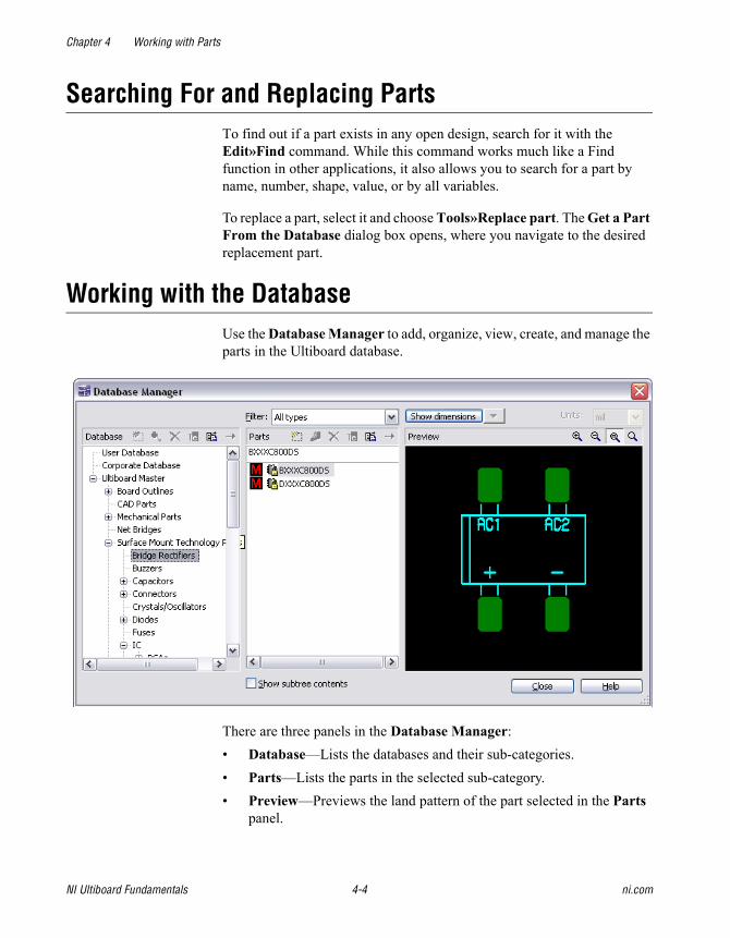
Working with the Database Use the Database Manager to add, organize, view, create, and manage the parts in the Ultiboard database.
There are three panels in the Database Manager:
• Database—Lists the databases and their sub-categories.
• Parts—Lists the parts in the selected sub-category.
• Preview—Previews the land pattern of the part selected in the Parts panel.
Chapter 4 Working with Parts
© National Instruments Corporation 4-5 NI Ultiboard Fundamentals
To make parts easier to locate, the database organizes them into categories and sub-categories. You can expand and collapse the categories and sub-categories in the Database Manager: click the plus (+) to expand a category or subcategory, and click the minus (–) to collapse it.
There are default categories and sub-categories, and you can create new ones if necessary. You can copy any database category and its contents to another category or sub-category. The sub-categories that appear by default cannot be deleted, renamed, or moved, but you can delete, rename, or move the ones that you have added.
© National Instruments Corporation 5-1 NI Ultiboard Fundamentals
5Working with Nets and Copper
This chapter explains some of the basics involved in working with nets and copper in Ultiboard.
Some of the described features may not be available in your edition of Ultiboard. Refer to the NI Circuit Design Suite Release Notes for a list of the features in your edition.
Refer to the Ultiboard Help for complete information on the features found in this chapter.
Nets The term net is used to describe the connection between pins on a schematic diagram. Nets represent either wires or traces on a printed circuit.
A netlist describes the connectivity of all nets in a design.
Ultiboard has a number of useful tools for working with nets:
• Net Edit dialog box—Use to view the nets in the design and to view the pins in the nets. You can also use it to add and delete nets from the design, add and delete pins from an existing net, adjust trace widths in a net, set high speed parameters and adjust a net’s via diameters and via drill hole size.
Chapter 5 Working with Nets and Copper
NI Ultiboard Fundamentals 5-2 ni.com
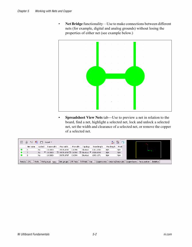
• Net Bridge functionality—Use to make connections between different nets (for example, digital and analog grounds) without losing the properties of either net (see example below.)
• Spreadsheet View Nets tab—Use to preview a net in relation to the board, find a net, highlight a selected net, lock and unlock a selected net, set the width and clearance of a selected net, or remove the copper of a selected net.
Chapter 5 Working with Nets and Copper
© National Instruments Corporation 5-3 NI Ultiboard Fundamentals
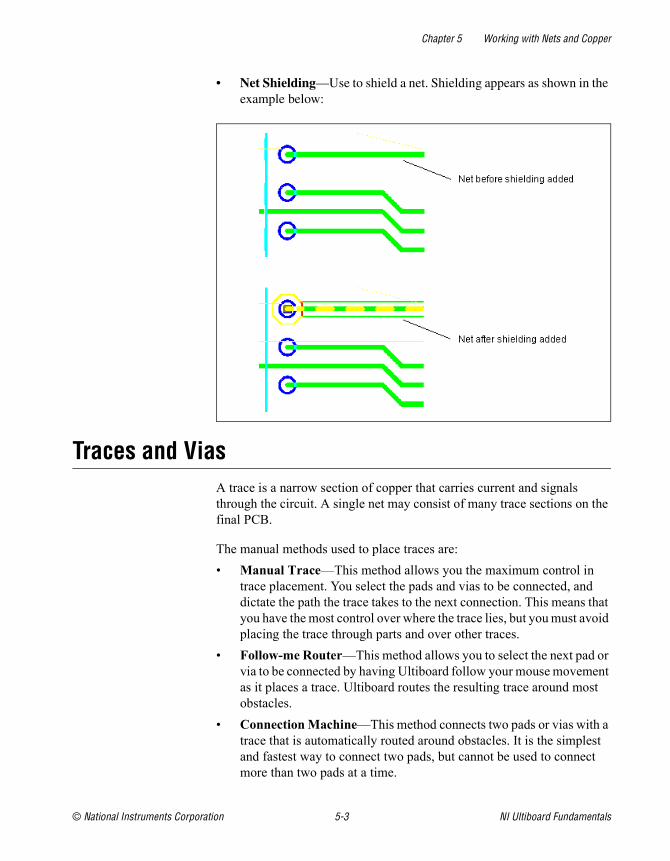
• Net Shielding—Use to shield a net. Shielding appears as shown in the example below:
Traces and Vias A trace is a narrow section of copper that carries current and signals through the circuit. A single net may consist of many trace sections on the final PCB.
The manual methods used to place traces are:
• Manual Trace—This method allows you the maximum control in trace placement. You select the pads and vias to be connected, and dictate the path the trace takes to the next connection. This means that you have the most control over where the trace lies, but you must avoid placing the trace through parts and over other traces.
• Follow-me Router—This method allows you to select the next pad or via to be connected by having Ultiboard follow your mouse movement as it places a trace. Ultiboard routes the resulting trace around most obstacles.
• Connection Machine—This method connects two pads or vias with a trace that is automatically routed around obstacles. It is the simplest and fastest way to connect two pads, but cannot be used to connect more than two pads at a time.
Chapter 5 Working with Nets and Copper
NI Ultiboard Fundamentals 5-4 ni.com
Note Depending on your edition of Ultiboard, you may also be able to place traces automatically. Refer to Chapter 6, Autoplacement and Autorouting, for details.
Tip Use the Place»Bus command to connect multiple traces between multi-pinned devices such as ICs.
A via is a plated through-hole used to connect two or more layers of a printed circuit board, as well as the top and bottom surfaces of the board. It can be used to connect parts on different layers or to route traces between layers.
As with other elements in an Ultiboard design, you can edit a via from its properties dialog box—select the via and choose Edit»Properties.
Copper As well as traces, an Ultiboard design may include copper areas and power planes.
A copper area is a copper polygon that takes up part of a layer.
A power plane is a copper area that covers an entire layer.
When you double-click on a copper element to display its properties dialog, the name of the dialog box that displays changes to reflect the selected element.
Tip A teardrop is a flare that you can add to a trace where the trace connects to a pad. Use this with very small sized traces, to prevent possible breakage in the copper between the trace and the pad.
Other Elements Other elements that you can include in your Ultiboard design include:
• Various shapes and graphics such as lines, circles.
• Mounting holes and connectors.
• Jumpers.
• Test points.
• Dimensions.
• Polygons.
• Keep-in/keep-out areas.
Chapter 5 Working with Nets and Copper
© National Instruments Corporation 5-5 NI Ultiboard Fundamentals
PCB Calculators To control reflections on high-speed PCBs, it is necessary to make the traces appear as if they are transmission lines. This is done by calculating the characteristic impedance of the trace (Zo) and then terminating it with its characteristic impedance. This makes the trace appear like an infinitely long transmission line, and it will therefore have no reflections, even though in reality it has a finite length. What actually occurs is that all of the energy that travels down the trace is absorbed, and there is no energy left to reflect back. Once you have calculated Zo, you can use it to design the trace’s termination.
There are a number of methods used to terminate transmission lines, for example, series termination, diode termination, which are beyond the scope of this help file. We recommend that you refer to any number of available texts on the subject.
Note Equations used are based on the IPC-D-317A document from the IPC organization (www.ipc.org).
Use the PCB Transmission Line Calculator to calculate the following parameters for typical printed circuit board trace geometries:
• Characteristic Impedance (Zo).
• Per unit length Capacitance (Co).
• Per unit length Inductance (Lo).
• Propogation Delay (tpd).
The PCB Transmission Line Calculator supports:
• Microstrip Trace Calculations.
• Embedded Microstrip Trace Calculations.
• Centered Stripline Trace Calculation.
• Asymmetric Stripline Trace Calculations.
• Dual Stripline Trace Calculations.
The PCB Differential Impedance Calculator performs calculations for two traces that carry signals that are exactly equal and opposite (a differential pair).
Use the PCB Differential Impedance Calculator to calculate the following parameters for differential pairs:
Chapter 5 Working with Nets and Copper
NI Ultiboard Fundamentals 5-6 ni.com
• Characteristic Impedance (Zo).
• Per unit length Capacitance (Co).
• Per unit length Inductance (Lo).
• Propogation Delay (tpd).
• Differential Impedance (Zdiff).
The PCB Differential Impedance Calculator supports:
• Microstrip Calculations.
• Embedded Microstrip Calculations.
• Centered Stripline Calculations.
• Asymmetric Stripline Calculations.
© National Instruments Corporation 6-1 NI Ultiboard Fundamentals
6Autoplacement and Autorouting
This chapter gives an overview of the autoplacment and autorouting features found in Ultiboard.
Some of the described features may not be available in your edition of Ultiboard. Refer to the NI Circuit Design Suite Release Notes for a list of the features in your edition.
Refer to the Ultiboard Help for complete information on the features found in this chapter.
Autoplacement The autoplacer automatically places all unplaced parts onto your board according to group settings you can specify. It uses a rip-up and retry algorithm to find the best part positioning. As the autoplacer runs, the status line at the bottom of the screen indicates how many autoplacement passes have been completed. It also indicates how many parts have been placed and how many pins have been swapped (when the autoplacer performs pin/gate swaps). If the autoplacer cannot place all the parts, it returns a message indicating how many parts are still unplaced in the Results tab of the Spreadsheet View.
The autoplacer places parts as clusters. These clusters are generated by grouping a multi-pin part with a series of connected parts, each of which has fewer than four pins. Each cluster is then assigned a placement priority. By arranging parts into clusters, the autoplacer can place together those parts that have multiple connections. Block capacitors, which are connected to power signals, are always excluded from clusters. Ultiboard uses automatic block capacitor recognition to place block capacitors close to their corresponding ICs.
Tip You may wish to pre-place certain parts (for example, holes) before autoplacing other parts.
Note The autoplacer is controlled from the Autoplace tab of the Routing Options dialog box.
Chapter 6 Autoplacement and Autorouting
NI Ultiboard Fundamentals 6-2 ni.com
Autorouting The autorouter runs an end-to-end autorouting process that includes four routing functions, applied in the following order:
1. Preprocessing.
2. Initial routing.
3. Rip-up and retry passes.
4. Optimization.
When you start the autorouter, Ultiboard analyzes the entire board, considering trace widths, clearances, keep-in, and keep-out areas. The preprocessor then determines the router parameters and algorithms best suited for this particular board, for example, routing grid size, pin clearance algorithms, and connection routing order.
Initial routing automatically routes as many traces as possible in a single pass without any rip-up and retry operations.
In some cases, Ultiboard can place all traces in a single pass without rerouting any traces. However, if Ultiboard does not achieve 100% completion, then the rip-up and retry router rips up selected traces and reroutes them to make room for other traces that could not be placed during the first pass.
The rip-up and retry router is guarded by a backtracking algorithm, which not only prevents routing deterioration or deadlock during rip-up and optimization, but is able to exploit better routing solutions. The rip-up and retry router automatically activates an intermediate optimizer if a single rip-up pass does not achieve 100% routing success.
Part of Ultiboard’s rip-up and retry procedure is to analyze dense board areas and adopt routing strategies in these areas, which decrease manufacturing costs. The cost factors Ultiboard uses can be adapted to your current routing problem; thus, you can control the routing strategies that Ultiboard uses and keep production costs within acceptable limits. It is strongly recommended that you do not modify these routing strategies unless you achieve poorer routing results than you expect with the defaults. When changing cost factors, even slight adjustments can have large effects on routing success, either improving or worsening the results.
The optimizer is usually applied after the autorouter achieves 100% completion. It eliminates unnecessary vias and smooths wire bends to reduce manufacturing costs. It also routes any remaining open connections.

Chapter 6 Autoplacement and Autorouting
© National Instruments Corporation 6-3 NI Ultiboard Fundamentals
Tip You can also autoroute selected buses and automatically place a test point on each net in your design.
Note Router functions are controlled through the Routing Options dialog box.
© National Instruments Corporation 7-1 NI Ultiboard Fundamentals
7Working with Schematic Capture
This chapter gives an overview of the features in Ultiboard that work in conjunction with Multisim, National Instruments’ schematic capture and simulation program.
Some of the described features may not be available in your edition of Ultiboard. Refer to the NI Circuit Design Suite Release Notes for a list of the features in your edition.
Refer to the Ultiboard Help for complete information on the features found in this chapter.
Creating a Design from a Netlist File Multisim can generate a .ewnet file which has all the details required to import the schematic into Ultiboard.
Once this file has been created, open Ultiboard, select File»Open, navigate to the desired .ewnet file and click Open.
Forward and Backward Annotation Forward Annotation is the process of sending schematic design changes to a corresponding PCB layout file.
When you do a forward annotation, the differences between the Multisim file and the Ultiboard file display in the Forward Annotation dialog box. You select from a list of possible actions for each difference.
Backward Annotation is the process of sending PCB layout changes to a corresponding schematic design.
When you do a backward annotation, the differences between the Ultiboard file and the Multisim file display in the Backward Annotation dialog box. You select from a list of possible actions for each difference.
Chapter 7 Working with Schematic Capture
NI Ultiboard Fundamentals 7-2 ni.com
Both forward and backward annotations are invoked from within Multisim or Ultiboard and provide the same user experience. A .ewnet file is produced during annotation that you can save and share. This file is the synchronization medium for both forward and backward annotation.
Cross-Probing Select a part, or group of parts in Ultiboard and use the Highlight Selection in Multisim command to have the corresponding components highlight in Multisim.
This is called cross-probing.
© National Instruments Corporation 8-1 NI Ultiboard Fundamentals
8Preparing for Manufacturing/Assembly
This chapter gives an overview of the features in Ultiboard that you can use to prepare your board for manufacturing.
Some of the described features may not be available in your edition of Ultiboard. Refer to the NI Circuit Design Suite Release Notes for a list of the features in your edition.
Refer to the Ultiboard Help for complete information on the features found in this chapter.
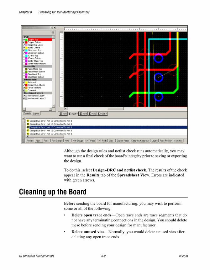
Design Rule Errors The design rules and netlist check normally runs automatically. Error details appear in the DRC tab. Double-click on an error in the DRC tab to zoom in on the affected area on the design, which is indicated with a red circle, as shown in the example below.
Chapter 8 Preparing for Manufacturing/Assembly
NI Ultiboard Fundamentals 8-2 ni.com
Although the design rules and netlist check runs automatically, you may want to run a final check of the board's integrity prior to saving or exporting the design.
To do this, select Design»DRC and netlist check. The results of the check appear in the Results tab of the Spreadsheet View. Errors are indicated with green arrows.
Cleaning up the Board Before sending the board for manufacturing, you may wish to perform some or all of the following:
• Delete open trace ends—Open trace ends are trace segments that do not have any terminating connections in the design. You should delete these before sending your design for manufacturer.
• Delete unused vias—Normally, you would delete unused vias after deleting any open trace ends.
Chapter 8 Preparing for Manufacturing/Assembly
© National Instruments Corporation 8-3 NI Ultiboard Fundamentals
• Renumber parts—As parts are added to, moved, and deleted from a design, their numbering changes. It is easier to produce, service, and troubleshoot boards when parts are ordered in a logical manner. You can use the Renumber Parts dialog box to renumber parts in the order that you specify.
• Miter corners—Use Corner Mitering to reduce or remove sharp angles on placed traces by creating 135° angles in their place. This is important for manufacturing purposes. You can apply corner mitering to the entire design or selected traces.
Documenting Your Design Ultiboard has a number of tools to help you document your design.
You can place and edit text anywhere on the design, and on any layer. You can also change the appearance and orientation of any placed text.
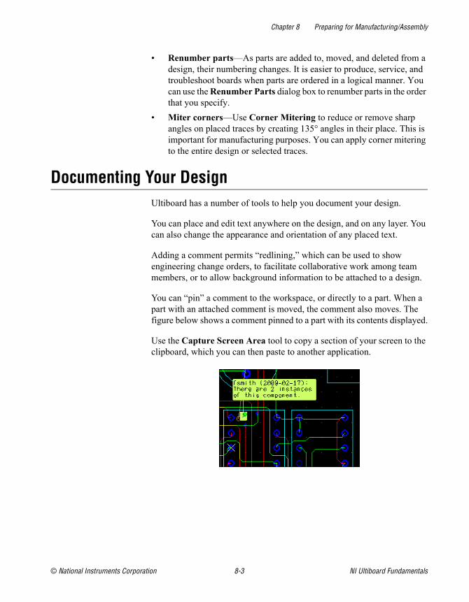
Adding a comment permits “redlining,” which can be used to show engineering change orders, to facilitate collaborative work among team members, or to allow background information to be attached to a design.
You can “pin” a comment to the workspace, or directly to a part. When a part with an attached comment is moved, the comment also moves. The figure below shows a comment pinned to a part with its contents displayed.
Use the Capture Screen Area tool to copy a section of your screen to the clipboard, which you can then paste to another application.
Chapter 8 Preparing for Manufacturing/Assembly
NI Ultiboard Fundamentals 8-4 ni.com
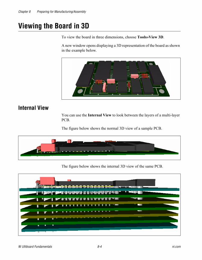
Viewing the Board in 3D To view the board in three dimensions, choose Tools»View 3D.
A new window opens displaying a 3D representation of the board as shown in the example below.
Internal View You can use the Internal View to look between the layers of a multi-layer PCB.
The figure below shows the normal 3D view of a sample PCB.
The figure below shows the internal 3D view of the same PCB.
Chapter 8 Preparing for Manufacturing/Assembly
© National Instruments Corporation 8-5 NI Ultiboard Fundamentals
Mechanical CAD Ultiboard’s mechanical CAD functionality can be used to design enclosure boxes, front panels, or any other mechanical part associated with your PCB design.
Mechanical CAD functionality in Ultiboard takes two forms:
• You can create multi-layer mechanical CAD design files.
• You can have mechanical CAD layers as part of your PCB design files. Design files can include up to 10 mechanical CAD layers. These are accessed through the Layers tab of the Design Toolbox and can be used in the same way as other layers in your design.
For the most part, you work with mechanical CAD designs the same way that you do with PCB designs, although you cannot place traces or use the Autoroute function in mechanical CAD designs.
Viewing Gerber Files Gerber files are the industry standard format for files used to generate PCBs. The industry standard version is the RS-274X file, which embeds aperture information into the file. For other versions of the Gerber format, a separate aperture file is needed. For each board design you will generally export multiple Gerber files, each of which will represent a specific layer on your PCB.
You can view one or more Gerber files before sending them for PCB manufacturing.
Chapter 8 Preparing for Manufacturing/Assembly
NI Ultiboard Fundamentals 8-6 ni.com
Exporting a File You can export a file from Ultiboard in a format that can be understood by the equipment at the board manufacturer. An exported file contains complete information describing how a finished board is to be manufactured. There are many different manufacturing techniques used to produce printed circuit boards and Ultiboard can produce a wide variety of outputs to meet these needs.
You can export files in the following formats:
• Gerber photoplotter 274X or 274D.
• DXF.
• 3D DXF.
• 3D IGES.
• IPC-D-356A Netlist.
• NC drill.
• SVG (Scalable Vector Graphics).
You can also export text files that contain:
• Board Statistics.
• Part Centroids.
• Bill of Materials.

Chapter 8 Preparing for Manufacturing/Assembly
© National Instruments Corporation 8-7 NI Ultiboard Fundamentals
You can also create reports on:
• Copper Amounts.
• Test Points.
• Layer Stackup.
© National Instruments Corporation A-1 NI Ultiboard Fundamentals
ATechnical Support and Professional Services
Visit the following sections of the award-winning National Instruments Web site at ni.com for technical support and professional services:
• Support—Technical support at ni.com/support includes the following resources:
– Self-Help Technical Resources—For answers and solutions, visit ni.com/support for software drivers and updates, a searchable KnowledgeBase, product manuals, step-by-step troubleshooting wizards, thousands of example programs, tutorials, application notes, instrument drivers, and so on. Registered users also receive access to the NI Discussion Forums at ni.com/forums. NI Applications Engineers make sure every question submitted online receives an answer.
– Standard Service Program Membership—This program entitles members to direct access to NI Applications Engineers via phone and email for one-to-one technical support, as well as exclusive access to eLearning training modules at ni.com/eLearning. NI offers complementary membership for a full year after purchase, after which you may renew to continue your benefits.
For information about other technical support options in your area, visit ni.com/services, or contact your local office at ni.com/contact.
• Training and Certification—Visit ni.com/training for training and certification program information. You can also register for instructor-led, hands-on courses at locations around the world.
• System Integration—If you have time constraints, limited in-house technical resources, or other project challenges, National Instruments Alliance Partner members can help. To learn more, call your local NI office or visit ni.com/alliance.
You also can visit the Worldwide Offices section of ni.com/niglobal to access the branch office Web sites, which provide up-to-date contact information, support phone numbers, email addresses, and current events.
© National Instruments Corporation I-1 NI Ultiboard Fundamentals
Index
Numerics3D view, using, 8-4
Aaperture files, 8-5autoplacing parts, 6-1autorouter, about, 6-2
Bbackward annotation, 7-1birds eye view, 2-6board annotation, 8-3board outline, creating, 3-3board, cleaning up before manufacturing, 8-2
Ccapturing screen area, 8-3conventions used in the manual, vicopper, 5-4copper areas, 5-4corner mitering, 8-2cross-probing, 7-2customizing interface, 2-6
DDatabase Manager, 4-4design rule check, 8-1design rule errors, 8-1Design Toolbox, overview, 2-5design, viewing in 3D, 8-4designs, 3-1diagnostic tools (NI resources), A-1
documentationconventions used in the manual, viNI resources, A-1
documenting your design, 8-3DRC and netlist check, 8-1drivers (NI resources), A-1
Eexamples (NI resources), A-1exporting files, 8-6
Ffinding parts, 4-4forward annotation, 7-1
Ggate swapping, 4-3Gerber files, 8-5Group Editor dialog, 3-3
Hhelp, technical support, A-1highlighting in Multisim, 7-2
IImport Netlist dialog box, 7-1instrument drivers (NI resources), A-1internal view, 8-4
KKnowledgeBase, A-1
Index
NI Ultiboard Fundamentals I-2 ni.com
Llayers, 3-2layout preferences, 2-3
Mmechanical CAD, 8-5
NNational Instruments support and
services, A-1net bridges, 5-1Net Edit dialog box, 5-1net shielding, 5-1netlist, opening, 7-1nets, 5-1
Oother design elements, 5-4
Ppart placement, 4-1PCB Calculators, 5-5PCB Differential Impedance Calculator, 5-5PCB Transmission Line Calculator, 5-5pin swapping, 4-3placing traces, 5-3power planes, 5-4programming examples (NI resources), A-1projects, 3-1property edits, 4-3
Rrenumbering parts, 8-2replacing parts, 4-4reports, 8-6Routing Options dialog box, 6-1, 6-2RS-274X files, 8-5
Ssoftware (NI resources), A-1Spreadsheet View, 2-4support, technical, A-1swapping
gates, 4-3pins, 4-3
Tteardrops, 5-4technical support, A-1Technology File Settings dialog box, 3-2technology files, 3-2text files, 8-6toolbars, 2-3training and certification (NI resources), A-1troubleshooting (NI resources), A-1
WWeb resources, A-1working with the database, 4-4


![Ultiboard Footprint Reference Guide[1]](https://img.pdfslide.net/doc/110x75/55cf91c2550346f57b905777/ultiboard-footprint-reference-guide1.jpg)