Embed Size (px)
Citation preview
NANOELECTRONICS
Nitride-based light-emitting diodes with InGaN/GaNSAQD active layers
L.W. Ji, Y.K. Su, S.J. Chang, S.C. Hung, C.S. Chang and L.W. Wu
Abstract: InGaN/GaN blue light-emitting diodes (LEDs) with self-assembled quantum dot(SAQD) active layers were successfully fabricated using an interrupted growth method in metal-organic chemical vapour deposition (MOCVD). Nanoscale QDs have been formed successfullyembedded in quantum wells (QWs) with a typical 3nm height and 10nm lateral dimension. A huge68.4meV blue shift in electroluminescence (EL) peak position was found as the injection currentwas increased from 3 to 50mA for the SAQD LED. The large EL blue shift reveals that deeplocalisation of exitons (or carriers) originating from QDs strengthens the band-filling effect as theinjection current increases.
1 Introduction
Heteroepitaxial growth of highly strained material systemsis attractive as it offers the possibility of producing low-dimensional carrier confinement nanostructures, such asquantum wells and self-assembled quantum dots (QDs) [1].III-nitride semiconductor materials have a wurtzite crystalstructure and a direct energy bandgap. One can also achievenitride-based heteroepitaxial growth easily. At roomtemperature, the bandgap energy of AlInGaN varies from0.7 to 6.2 eV, dependent on its composition. Therefore, III-nitride semiconductors are particularly useful for light-emitting diodes (LEDs) and laser diodes (LDs) in thiswavelength region [2–5]. Typical high-brightness LEDshave a multiple quantum well (MQW) active region. TheMQW LED is a kind of heterojunction device, in whichelectrons and holes are confined to the well layers. One canachieve high quantum efficiency from MQW LEDs sincecarriers can recombine easily in the confined well layers [6–9]. Although high brightness InGaN/GaNMQWLEDs arealready commercially available, it should be possible toenhance LED output intensity by using QDs, instead ofMQWs, to further confine the carriers.
Recently, it has been shown that nitride nanostructurescan be self-organised using the strain-induced Stranski–Krastanov (S–K) growth mode without any substratepatterning process [10–12]. It has also been shown thatnitride nanostructures can be self-organised using growthinterruption during metal-organic chemical vapour deposi-tion (MOCVD) growth [13]. Although the size fluctuationsof self-assembled QDs could result in inhomogeneousoptical and electrical characteristics, the self-assembly ofstrain-induced islands provides the means for creating zero-dimensional quantum structures without having to over-come the current limitations of lithography. These self-
assembled QDs could also be used to study novel devicephysics [14–16]. In this work, we report the fabrication ofblue LEDs with InGaN/GaN multiple quantum dot(MQD) structure. The optical and electrical properties ofthe InGaN/GaN MQD LEDs are also reported.
2 Experiment
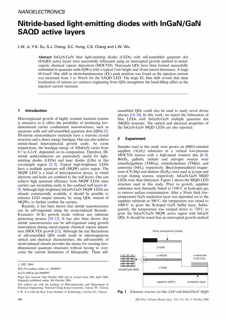
Samples used in this study were grown on (0001)-orientedsapphire (Al2O3) substrates in a vertical low-pressureMOCVD reactor with a high-speed rotation disc [6–9].Briefly, gallium, indium and nitrogen sources weretrimethylgallium (TMGa), trimethylindium (TMIn), andammonia (NH3), respectively. Biscyclopentadienyl magne-sium (CP2Mg) and disilane (Si2H6) were used as p-type andn-type doping sources, respectively. InGaN/GaN MQDLEDs were then fabricated. Figure 1 shows the MQD LEDstructure used in this study. Prior to growth, sapphiresubstrates were thermally baked at 11001C in hydrogen gasto remove surface contamination. After a 30nm thick low-temperature GaN nucleation layer was deposited on to thesapphire substrate at 5001C, the temperature was raised to10001C to grow the Si-doped GaN buffer layer. Subse-quently, the temperature was ramped down to 7301C togrow the InGaN/GaN MQW active region with InGaNQDs. It should be noted that an interrupted growth method
n-GaN
p-AlGaN
p-GaN
Ni/Au transparent contact
n-electrodeTi/Al/Ti/Au
sapphire (0001) nucleation layer
InGaN/GaN MQD
Fig. 1 Schematic structure for blue LED with InGaN/GaN MQD
The authors are with the Institute of Microelectronics and Department ofElectrical Engineering, National Cheng Kung University, Tainan 701, Taiwan
L.W. Ji is with the Kao Yuan Institute of Technology, Lu-Chu 821, Taiwan
r IEE, 2004
IEE Proceedings online no. 20040997
doi:10.1049/ip-cds:20040997
Paper first received 16th October 2003 and in revised form 29th April 2004.Originally published online: 8th October 2004
486 IEE Proc.-Circuits Devices Syst., Vol. 151, No. 5, October 2004
was used so as to achieve InGaN QD well layers. That is,we first deposited a 1.2nm thick InGaN layer, stopped thegrowth for 12 s, and then deposited another 1.2nm thickInGaN layer so as to achieve a 2.4nm nominal thickness ofInGaN [13]. In the active region, each InGaN/GaN pairconsists of a 2.4nm thick InGaN QD well layer and a15nm thick GaN barrier layer. The InGaN QD well layerswere unintentionally doped, and the GaN barrier layerswere Si-doped with a doping concentration of 3� 1017 cm�3
[9]. After growth of the active region, the substratetemperature was elevated to 10601C again to grow theMg-doped AlGaN cladding layer and Mg-doped GaNcontact layer. In order to increase the indium incorporationrate, nitrogen was used as the carrier gas when the InGaN/GaNMQD active regions were grown. Hydrogen was usedas the carrier gas when other parts of the samples weregrown. The growth pressure was kept at 350mtorrthroughout growth. The as-grown samples were thenannealed at 7601C for 25 min in N2 ambient to activatethe Mg-doped p-type layers. With this thermal annealingprocess, we could achieve uniformly doped highly con-ductive p-type layers. For LED fabrication, the surfaces ofthe p-type layers were partially etched until the n-type GaNlayers were exposed. Ni/Au contacts were subsequentlyevaporated on to the p-type GaN surfaces to serve as p-electrodes. Ti/Al/Ti/Au contacts were deposited on to theexposed n-type GaN layers to serve as n-type electrodes, tocomplete fabrication of the blue LEDs.
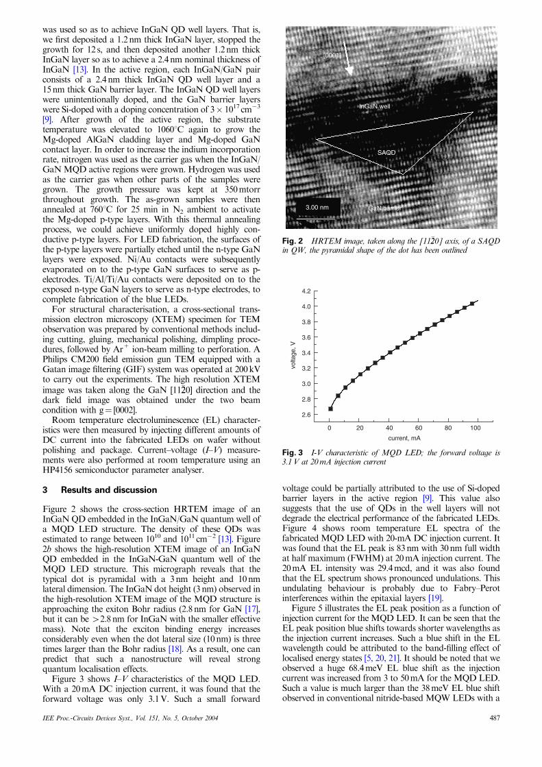
For structural characterisation, a cross-sectional trans-mission electron microscopy (XTEM) specimen for TEMobservation was prepared by conventional methods includ-ing cutting, gluing, mechanical polishing, dimpling proce-dures, followed by Ar+ ion-beam milling to perforation. APhilips CM200 field emission gun TEM equipped with aGatan image filtering (GIF) system was operated at 200kVto carry out the experiments. The high resolution XTEMimage was taken along the GaN [11�220] direction and thedark field image was obtained under the two beamcondition with g¼ [0002].
Room temperature electroluminescence (EL) character-istics were then measured by injecting different amounts ofDC current into the fabricated LEDs on wafer withoutpolishing and package. Current–voltage (I–V) measure-ments were also performed at room temperature using anHP4156 semiconductor parameter analyser.
3 Results and discussion
Figure 2 shows the cross-section HRTEM image of anInGaN QD embedded in the InGaN/GaN quantum well ofa MQD LED structure. The density of these QDs wasestimated to range between 1010 and 1011 cm�2 [13]. Figure2b shows the high-resolution XTEM image of an InGaNQD embedded in the InGaN-GaN quantum well of theMQD LED structure. This micrograph reveals that thetypical dot is pyramidal with a 3nm height and 10nmlateral dimension. The InGaN dot height (3nm) observed inthe high-resolution XTEM image of the MQD structure isapproaching the exiton Bohr radius (2.8nm for GaN [17],but it can be 42.8nm for InGaN with the smaller effectivemass). Note that the exciton binding energy increasesconsiderably even when the dot lateral size (10nm) is threetimes larger than the Bohr radius [18]. As a result, one canpredict that such a nanostructure will reveal strongquantum localisation effects.
Figure 3 shows I–V characteristics of the MQD LED.With a 20mA DC injection current, it was found that theforward voltage was only 3.1V. Such a small forward
voltage could be partially attributed to the use of Si-dopedbarrier layers in the active region [9]. This value alsosuggests that the use of QDs in the well layers will notdegrade the electrical performance of the fabricated LEDs.Figure 4 shows room temperature EL spectra of thefabricated MQD LED with 20-mA DC injection current. Itwas found that the EL peak is 83nm with 30nm full widthat half maximum (FWHM) at 20mA injection current. The20mA EL intensity was 29.4mcd, and it was also foundthat the EL spectrum shows pronounced undulations. Thisundulating behaviour is probably due to Fabry–Perotinterferences within the epitaxial layers [19].
Figure 5 illustrates the EL peak position as a function ofinjection current for the MQD LED. It can be seen that theEL peak position blue shifts towards shorter wavelengths asthe injection current increases. Such a blue shift in the ELwavelength could be attributed to the band-filling effect oflocalised energy states [5, 20, 21]. It should be noted that weobserved a huge 68.4meV EL blue shift as the injectioncurrent was increased from 3 to 50mA for the MQD LED.Such a value is much larger than the 38meV EL blue shiftobserved in conventional nitride-based MQW LEDs with a
SAQD
GaN barrier
InGaN well
[0001]
3.00 nm
Fig. 2 HRTEM image, taken along the [11�220] axis, of a SAQDin QW, the pyramidal shape of the dot has been outlined
0 20 40 60 80 100
2.6
2.8
3.0
3.2
3.4
3.6
3.8
4.0
4.2vo
ltage
, V
current, mA
Fig. 3 I-V characteristic of MQD LED; the forward voltage is3.1 V at 20 mA injection current
IEE Proc.-Circuits Devices Syst., Vol. 151, No. 5, October 2004 487
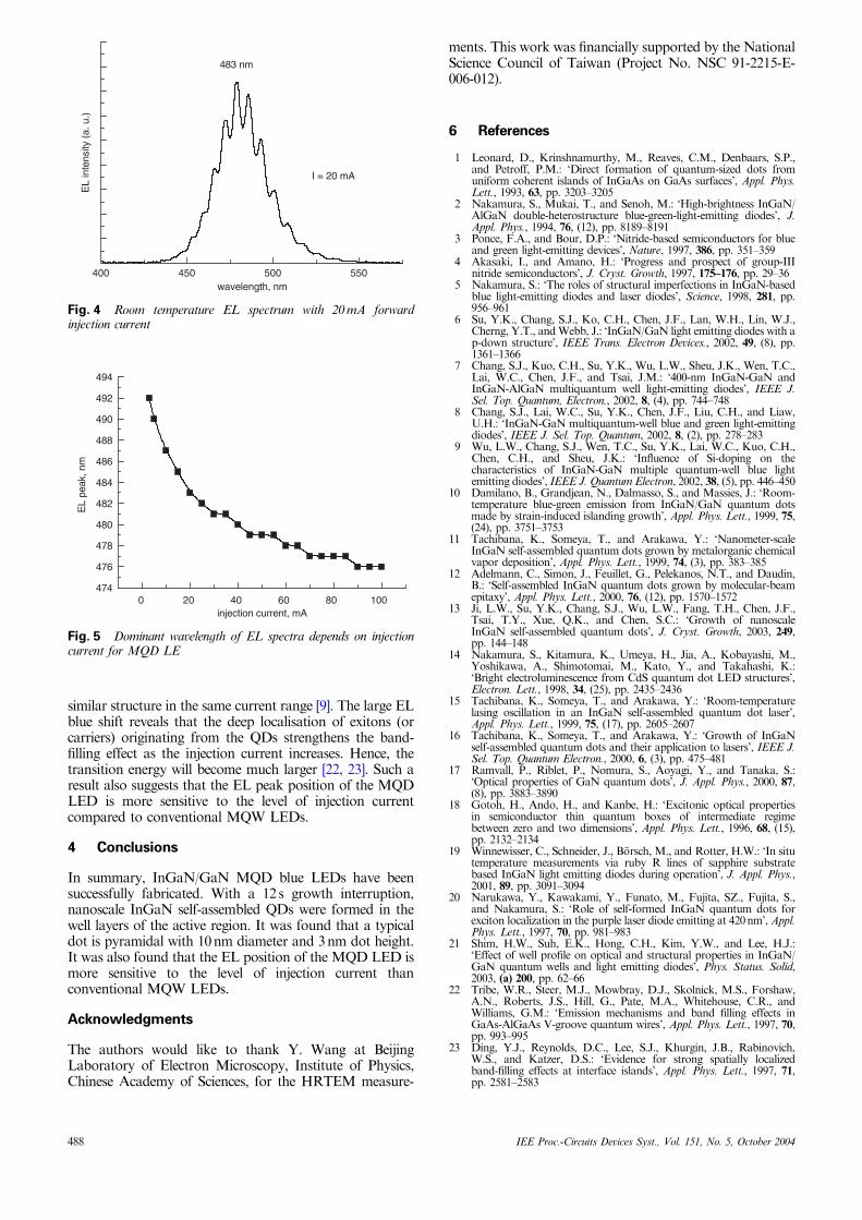
similar structure in the same current range [9]. The large ELblue shift reveals that the deep localisation of exitons (orcarriers) originating from the QDs strengthens the band-filling effect as the injection current increases. Hence, thetransition energy will become much larger [22, 23]. Such aresult also suggests that the EL peak position of the MQDLED is more sensitive to the level of injection currentcompared to conventional MQW LEDs.
4 Conclusions
In summary, InGaN/GaN MQD blue LEDs have beensuccessfully fabricated. With a 12 s growth interruption,nanoscale InGaN self-assembled QDs were formed in thewell layers of the active region. It was found that a typicaldot is pyramidal with 10nm diameter and 3nm dot height.It was also found that the EL position of the MQD LED ismore sensitive to the level of injection current thanconventional MQW LEDs.
Acknowledgments
The authors would like to thank Y. Wang at BeijingLaboratory of Electron Microscopy, Institute of Physics,Chinese Academy of Sciences, for the HRTEM measure-
ments. This work was financially supported by the NationalScience Council of Taiwan (Project No. NSC 91-2215-E-006-012).
6 References
1 Leonard, D., Krinshnamurthy, M., Reaves, C.M., Denbaars, S.P.,and Petroff, P.M.: ‘Direct formation of quantum-sized dots fromuniform coherent islands of InGaAs on GaAs surfaces’, Appl. Phys.Lett., 1993, 63, pp. 3203–3205
2 Nakamura, S., Mukai, T., and Senoh, M.: ‘High-brightness InGaN/AlGaN double-heterostructure blue-green-light-emitting diodes’, J.Appl. Phys., 1994, 76, (12), pp. 8189–8191
3 Ponce, F.A., and Bour, D.P.: ‘Nitride-based semiconductors for blueand green light-emitting devices’, Nature, 1997, 386, pp. 351–359
4 Akasaki, I., and Amano, H.: ‘Progress and prospect of group-IIInitride semiconductors’, J. Cryst. Growth, 1997, 175–176, pp. 29–36
5 Nakamura, S.: ‘The roles of structural imperfections in InGaN-basedblue light-emitting diodes and laser diodes’, Science, 1998, 281, pp.956–961
6 Su, Y.K., Chang, S.J., Ko, C.H., Chen, J.F., Lan, W.H., Lin, W.J.,Cherng, Y.T., andWebb, J.: ‘InGaN/GaN light emitting diodes with ap-down structure’, IEEE Trans. Electron Devices., 2002, 49, (8), pp.1361–1366
7 Chang, S.J., Kuo, C.H., Su, Y.K., Wu, L.W., Sheu, J.K., Wen, T.C.,Lai, W.C., Chen, J.F., and Tsai, J.M.: ‘400-nm InGaN-GaN andInGaN-AlGaN multiquantum well light-emitting diodes’, IEEE J.Sel. Top. Quantum, Electron., 2002, 8, (4), pp. 744–748
8 Chang, S.J., Lai, W.C., Su, Y.K., Chen, J.F., Liu, C.H., and Liaw,U.H.: ‘InGaN-GaN multiquantum-well blue and green light-emittingdiodes’, IEEE J. Sel. Top. Quantum, 2002, 8, (2), pp. 278–283
9 Wu, L.W., Chang, S.J., Wen, T.C., Su, Y.K., Lai, W.C., Kuo, C.H.,Chen, C.H., and Sheu, J.K.: ‘Influence of Si-doping on thecharacteristics of InGaN-GaN multiple quantum-well blue lightemitting diodes’, IEEE J. Quantum Electron, 2002, 38, (5), pp. 446–450
10 Damilano, B., Grandjean, N., Dalmasso, S., and Massies, J.: ‘Room-temperature blue-green emission from InGaN/GaN quantum dotsmade by strain-induced islanding growth’, Appl. Phys. Lett., 1999, 75,(24), pp. 3751–3753
11 Tachibana, K., Someya, T., and Arakawa, Y.: ‘Nanometer-scaleInGaN self-assembled quantum dots grown by metalorganic chemicalvapor deposition’, Appl. Phys. Lett., 1999, 74, (3), pp. 383–385
12 Adelmann, C., Simon, J., Feuillet, G., Pelekanos, N.T., and Daudin,B.: ‘Self-assembled InGaN quantum dots grown by molecular-beamepitaxy’, Appl. Phys. Lett., 2000, 76, (12), pp. 1570–1572
13 Ji, L.W., Su, Y.K., Chang, S.J., Wu, L.W., Fang, T.H., Chen, J.F.,Tsai, T.Y., Xue, Q.K., and Chen, S.C.: ‘Growth of nanoscaleInGaN self-assembled quantum dots’, J. Cryst. Growth, 2003, 249,pp. 144–148
14 Nakamura, S., Kitamura, K., Umeya, H., Jia, A., Kobayashi, M.,Yoshikawa, A., Shimotomai, M., Kato, Y., and Takahashi, K.:‘Bright electroluminescence from CdS quantum dot LED structures’,Electron. Lett., 1998, 34, (25), pp. 2435–2436
15 Tachibana, K., Someya, T., and Arakawa, Y.: ‘Room-temperaturelasing oscillation in an InGaN self-assembled quantum dot laser’,Appl. Phys. Lett., 1999, 75, (17), pp. 2605–2607
16 Tachibana, K., Someya, T., and Arakawa, Y.: ‘Growth of InGaNself-assembled quantum dots and their application to lasers’, IEEE J.Sel. Top. Quantum Electron., 2000, 6, (3), pp. 475–481
17 Ramvall, P., Riblet, P., Nomura, S., Aoyagi, Y., and Tanaka, S.:‘Optical properties of GaN quantum dots’, J. Appl. Phys., 2000, 87,(8), pp. 3883–3890
18 Gotoh, H., Ando, H., and Kanbe, H.: ‘Excitonic optical propertiesin semiconductor thin quantum boxes of intermediate regimebetween zero and two dimensions’, Appl. Phys. Lett., 1996, 68, (15),pp. 2132–2134
19 Winnewisser, C., Schneider, J., B.orsch, M., and Rotter, H.W.: ‘In situtemperature measurements via ruby R lines of sapphire substratebased InGaN light emitting diodes during operation’, J. Appl. Phys.,2001, 89, pp. 3091–3094
20 Narukawa, Y., Kawakami, Y., Funato, M., Fujita, SZ., Fujita, S.,and Nakamura, S.: ‘Role of self-formed InGaN quantum dots forexciton localization in the purple laser diode emitting at 420nm’, Appl.Phys. Lett., 1997, 70, pp. 981–983
21 Shim, H.W., Suh, E.K., Hong, C.H., Kim, Y.W., and Lee, H.J.:‘Effect of well profile on optical and structural properties in InGaN/GaN quantum wells and light emitting diodes’, Phys. Status. Solid,2003, (a) 200, pp. 62–66
22 Tribe, W.R., Steer, M.J., Mowbray, D.J., Skolnick, M.S., Forshaw,A.N., Roberts, J.S., Hill, G., Pate, M.A., Whitehouse, C.R., andWilliams, G.M.: ‘Emission mechanisms and band filling effects inGaAs-AlGaAs V-groove quantum wires’, Appl. Phys. Lett., 1997, 70,pp. 993–995
23 Ding, Y.J., Reynolds, D.C., Lee, S.J., Khurgin, J.B., Rabinovich,W.S., and Katzer, D.S.: ‘Evidence for strong spatially localizedband-filling effects at interface islands’, Appl. Phys. Lett., 1997, 71,pp. 2581–2583
400 450 500 550
483 nm
I = 20 mA
EL
inte
nsity
(a.
u.)
wavelength, nm
Fig. 4 Room temperature EL spectrum with 20 mA forwardinjection current
0 20 40 60 80 100474
476
478
480
482
484
486
488
490
492
494
EL
peak
, nm
injection current, mA
Fig. 5 Dominant wavelength of EL spectra depends on injectioncurrent for MQD LE
488 IEE Proc.-Circuits Devices Syst., Vol. 151, No. 5, October 2004


![Enhancement of InGaN-Based Light Emitting Diodes ...InGaN-based light-emitting diodes (LEDs) are useful for a wide range of visible light applications [1]-[4]. They *Corresponding](https://img.pdfslide.net/doc/110x75/60f8714d107e0617217e0a1d/enhancement-of-ingan-based-light-emitting-diodes-ingan-based-light-emitting.jpg)