Embed Size (px)
Citation preview

NMI TR 12
Nanometrology: The Critical Role of Measurement in Supporting Australian Nanotechnology
Dr John Miles
First edition — November 2006
Bradfield Road, Lindfield, NSW 2070PO Box 264, Lindfield, NSW 2070
Telephone: (61 2) 8467 3600Facsimile: (61 2) 8467 3610Web page: http://www.measurement.gov.au

© Commonwealth of Australia 2006
CONTENTSAcronyms......................................................................................................................iv
Summary........................................................................................................................v
1. Introduction............................................................................................................1
2. Nanotechnology Activities.....................................................................................32.1 USA..............................................................................................................52.2 Canada..........................................................................................................52.3 Asia–Pacific.................................................................................................62.4 Europe..........................................................................................................72.5 Australia.......................................................................................................8
3. Nanoparticle Activity in Australia.......................................................................103.1 Commercial Activity..................................................................................113.2 Research.....................................................................................................11
4. Nanometrology.....................................................................................................124.1 Nanometrology Infrastructure....................................................................134.2 Development of Standards and Regulations..............................................14
5. Nanometrology Methods and Instruments...........................................................165.1 Electron Microscopy..................................................................................165.2 Scanning Probe Microscopy.......................................................................175.3 Adding a Length Scale...............................................................................195.4 Traceability for Nanoscale Measurements.................................................195.5 Nanoparticle Measuring Instruments.........................................................205.6 Traceability of Nanoparticle Measuring Instruments.................................22
6. Nanometrology — International Activities..........................................................236.1 National Institute of Science and Technology (USA)................................236.2 National Metrology Institute of Japan........................................................256.3 Korean Research Institute of Standards and Science.................................256.4 Physikalisch-Technische Bundesanstalt (Germany)..................................266.5 National Physical Laboratory (UK)...........................................................276.6 Centre for Measurement Standards, Industrial Technology Research
Institute (Taiwan).......................................................................................286.7 Standards Productivity and Innovation Board (Singapore)........................286.8 Institute for National Measurement Standards (Canada)...........................286.9 National Institute of Metrology (China).....................................................296.10 National Institute of Metrology, Standardisation and Industrial Quality
(Brazil).......................................................................................................296.11 National Measurement Institute (Australia)...............................................296.12 Asia–Pacific Economic Cooperation.........................................................306.13 International Bureau of Weights and Measures.........................................31
7. Conclusions and Recommendations.....................................................................31
Appendix A Australian Nanoparticle Companies........................................................34
Appendix B Australian Nanoparticle Research Institutions........................................37
References....................................................................................................................43
iii

ACRONYMSAFM atomic force microscope
APEC Asia–Pacific Economic Cooperation
BIPM International Bureau of Weights and Measures
CMS Centre for Measurement Standards, Industrial Technology Research Institute (Taiwan)
CSIRO Commonwealth Scientific and Industry Research Organisation
EM electron microscope
INMETRO National Institute of Metrology, Standardisation and Industrial Quality (Brazil)
INMS Institute for National Measurement Standards (Canada)
KRISS Korean Research Institute of Standards and Science
NIM National Institute of Metrology (China)
NIST National Institute of Science and Technology (USA)
NMI National Measurement Institute (Australia)
NMIJ National Metrology Institute of Japan
NPL National Physical Laboratory (UK)
PTB Physikalisch-Technische Bundesanstalt (Germany)
SEM scanning electron microscope
SI international system of units
SPM scanning probe microscope
SPRING Standards Productivity and Innovation Board (Singapore)
TEM transmission electron microscope
iv

SUMMARYThe National Measurement Institute (NMI) has conducted an investigation into the needs of Australia’s emerging nanotechnology industry for measurement support focussing on dimensional (length) metrology and nanoparticles, i.e. particles with one or more dimensions of the order of 100 nm or less. The main finding is that NMI should immediately commence a program of establishing nanometrology infrastructure to support the emerging nanotechnology industry. However, this program cannot commence without additional resourcing.
The following gives a more detailed summary of the findings of the investigation.
Nanotechnology is a global phenomenon that will impact significantly on Australia’s scientific, technological, economic and social development. It has the potential to be one of Australia’s main sources of productivity growth. It also offers Australian industry an opportunity to move up the value chain and remain competitive as it demands long-term, strategic research and development, innovation and interdisciplinary work.
In Australia, nanotechnology is relatively strong in the research sector and is beginning to emerge in the business sector. Those Australian companies currently engaged in nanotechnology are predominantly involved with manufacturing nanoparticles.
Nanoproducts include cosmetics and sunscreens, ultra-violet resistant coatings on bottles, stain-resistant and wrinkle-free textiles and nucleating agents. A number of Australian companies are exporting their products to Asia, Europe and North America. The economic significance of these companies may be described as small but growing rapidly. All are optimistic about their future growth.
The emergence of nanotechnology as a high-technology industry that truly enhances the quality of life of its citizens depends crucially on the provision of a suitable scientific, commercial and regulatory environment.
A fundamental element of this environment is measurement. Metrology is the science of measurement and a metrological infrastructure has underpinned all industrial revolutions. Nanotechnology will be no exception. Accurate and reliable measurements of physical, chemical and biological quantities are required at all stages of the nanotechnology value chain to truly understand and control the manufacturing process and ensure and demonstrate product quality.
Consequently, the national metrology institutes of most industrialised economies are developing nanometrology infrastructures, initially for dimensional (length) measurements. The International Bureau of Weights and Measures’ Consultative Committee for Length has already coordinated several international national metrology institutes comparisons of dimensional nanometrology standards. Eventually, the entire spectrum of measurements, including electrical, optical, magnetic, mechanical, chemical and biological measurements, will be part of these nanometrological infrastructures.
A nanometrology infrastructure is also a prerequisite for documentary standards and regulations involving nanotechnology, which to be effective must be written in terms of measurable quantities and levels, tolerances and uncertainties, incorporating reliable measurement instruments and techniques.
Australia has only a rudimentary nanometrology infrastructure and this will hinder the emergence of nanotechnology in Australia. Nanocompanies, research institutions and regulatory authorities are already encountering measurement problems, particularly regarding nanoparticle measurement. This is impacting on production, quality control
v

and international business and on the ability of regulatory authorities to generate effective legislation and regulation. A high-quality nanometrological infrastructure would resolve many of these problems and this report recommends that NMI immediately commence a program of establishing a nanometrology infrastructure in Australia, concentrating initially on length metrology and nanoparticles.
The proposed nanometrology infrastructure will link practical measurements made in the nanotechnology community to the international system of units (SI), embodied in the Australian national standards of measurement, through a hierarchy of measurement standards. A practical measurement that is linked to SI units in this way is called an SI traceable measurement, i.e. traceable to internationally recognised measurement standards and units. The infrastructure ensures that measurements can be made on a consistent basis throughout the country and in-line with international measurement practices.
NMI’s program would initially concentrate on two tasks.
The first would be to establish physical standards and instruments capable of transferring Australia’s realisation of the metre, using known optical wavelengths of light, down to nanometre measurements in the nanotechnology community via a chain of comparisons.
The recommended method is to develop three high level instruments: a metrological atomic force microscope, an optical diffractometer and an interference microscope. These instruments are capable of calibrating artefacts such as gratings, grids and step height standards directly in terms of optical wavelengths. These artefacts would then be used to calibrate a wide range of standards and instruments used in the nanotechnology community, including standard reference powders, scanning probe microscopes and electron microscopes.
The second task is to establish a laboratory for nanoparticle standards and measurement containing instruments used in Australian companies and institutions. The laboratory would disseminate nanoparticle standards via cost-recovery testing and a calibration service. It would also conduct proficiency testing, run training courses, publish standard operating procedures and participate in international comparisons.
An important function of the laboratory will be to investigate and resolve measurement issues and problems associated with nanoparticle instruments. This work should be done in close collaboration with the nanotechnology community and include exploring the limitations, accuracy and characteristics of the instruments and the influence of testing environments and sample preparation.
The acquisition of technology and expertise implicit in both tasks would establish NMI as a national resource for technology transfer and measurement-related expertise for nanometrology.
An extremely important role for NMI is to maintain close links with international and regional measurement and standards institutions and organisations. The aim of these connections is to monitor overseas technical and regulatory developments and transfer them back to the Australian nanotechnology community.
Nanometrology offers NMI a unique opportunity for interdisciplinary and interbranch projects on measurement standards for nanobiotechnology and nanochemistry, both of which are extremely active and developing fields. There is a real need to combine the work of the chemical and biological metrology, physical, analytical and even the legal metrology branches.
vi

1. INTRODUCTION
Nanotechnology will be as influential in the 21st century as information technology was in the 20th century.
Few areas of our lives will fail to be impacted by nanotechnology … The US National Science Foundation forecasts that by 2011–15,
markets for nanomaterials with special properties and processes will reach US$240 billion per annum. Australia will be at the forefront of
this technological revolution as it sweeps the world.
The Hon Ian Macfarlane MP, Minister for Industry, Tourism and Resources [1]
Agreement on a definition of nanotechnology is only beginning to emerge. An influential study by The Royal Society and The Royal Academy of Engineering entitled Nanoscience and Nanotechnologies: Opportunities and Uncertainties [2] states that:
Nanoscience is the study of phenomena and manipulation of materials at atomic, molecular and macromolecular scales, where properties differ significantly from those at a larger scale.
Nanotechnologies are the design, characterisation, production and application of structures, devices and systems by controlling shape and size at nanometre scale.
A more operational definition of nanotechnology [3] is:
Research and technology development at the atomic, molecular, or macromolecular levels, in the length scale of approximately 1 to 100 nm range, to provide a fundamental understanding of phenomena and materials properties at the nanoscale and to model, create, characterise, manipulate, and use structures, devices, and systems that have novel properties and functions because of their small or intermediate size. The novel and differentiating properties and function are developed at a critical length scale of matter typically under 100 nm. Nanotechnology research and development includes integration of nanoscale structure into larger material components, systems and architectures. Within these larger scale assemblies, the control and construction of their structures and components devices remain at the nanometre scale.
The size range from 100 nm down to the atomic level is of interest because in this range materials can have very different properties compared with the same materials with a larger size. This is due to the increased relative surface area and the dominance of quantum effects. An increase in surface area leads to an increase in chemical reactivity and below tens of nanometres, quantum effects can significantly change a material’s optical, magnetic or electrical properties.
It is important to understand that nanotechnology is a collective term for a multidisciplinary grouping of physical, chemical, biological, engineering and electronic, processes, materials, applications and concepts in which the defining characteristic is one of size. It operates across the value-add chain, with a diversity of applications and products, ranging from electronics, optical communications and biological systems, to new materials. Nanotechnology is often said to be an enabling set of technologies or tools [2].
NMI TR 12 1

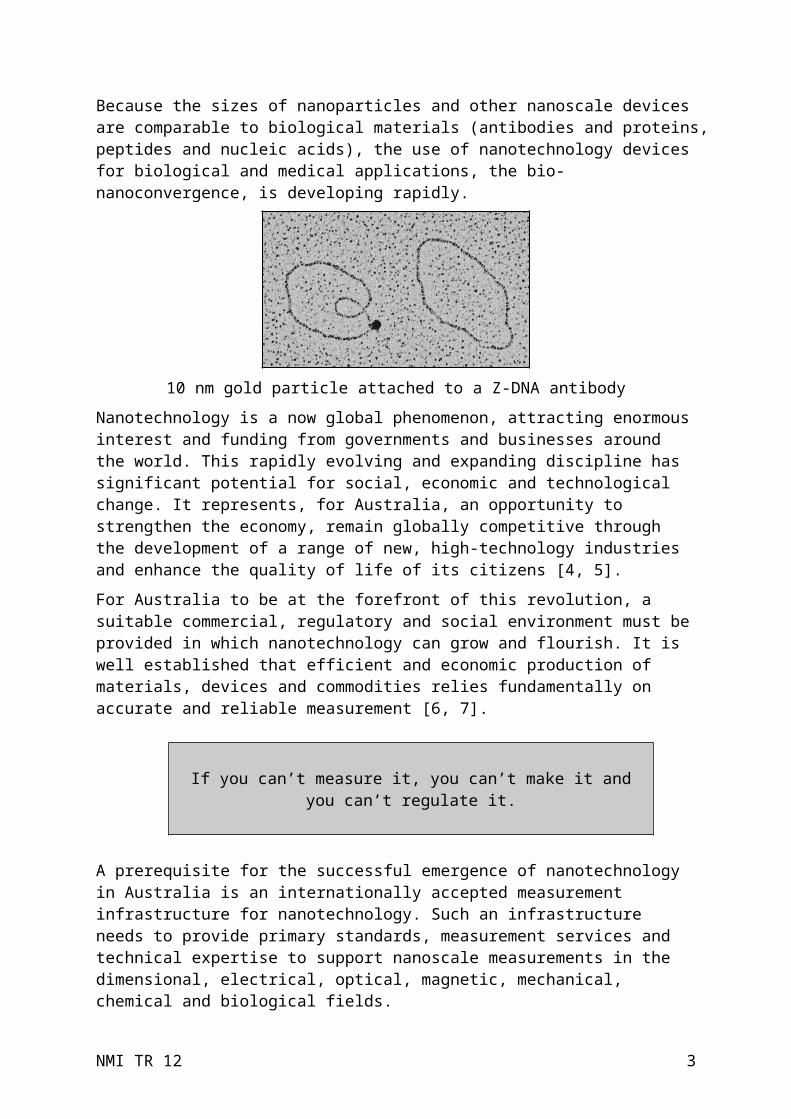
Because the sizes of nanoparticles and other nanoscale devices are comparable to biological materials (antibodies and proteins, peptides and nucleic acids), the use of nanotechnology devices for biological and medical applications, the bio-nanoconvergence, is developing rapidly.
10 nm gold particle attached to a Z-DNA antibody
Nanotechnology is a now global phenomenon, attracting enormous interest and funding from governments and businesses around the world. This rapidly evolving and expanding discipline has significant potential for social, economic and technological change. It represents, for Australia, an opportunity to strengthen the economy, remain globally competitive through the development of a range of new, high-technology industries and enhance the quality of life of its citizens [4, 5].
For Australia to be at the forefront of this revolution, a suitable commercial, regulatory and social environment must be provided in which nanotechnology can grow and flourish. It is well established that efficient and economic production of materials, devices and commodities relies fundamentally on accurate and reliable measurement [6, 7].
If you can’t measure it, you can’t make it and you can’t regulate it.
A prerequisite for the successful emergence of nanotechnology in Australia is an internationally accepted measurement infrastructure for nanotechnology. Such an infrastructure needs to provide primary standards, measurement services and technical expertise to support nanoscale measurements in the dimensional, electrical, optical, magnetic, mechanical, chemical and biological fields.
Recognising this, NMI has conducted an investigation into how it can best support the emergence of nanotechnology in Australia. This report presents the results of the investigation.
The terms of reference for the report were:
to determine the level of activity in Australia and internationally, including the number of companies, their economic significance, the type of activity etc;
to use this information to define and scope the size range of particles that underpin and enable emerging nanotechnologies and focus on these;
to investigate the current and potential applications of nanoparticles as defined in this scope;
to determine the role played by the International Bureau of Weights and Measures and national metrology institutes in other countries;
NMI TR 12 2

to determine the demand in Australian industry for traceability, technical support and research and development, and the current role of alternative suppliers, such as the National Association of Testing Authorities;
to determine current capability within NMI and the requirements if we decide to establish a facility; and
to prepare a business case, if required, for the establishment of a nanoparticle size measurement facility within NMI.
Nanotechnology is a large, rapidly evolving field, difficult to capture and summarise. This investigation narrowed its focus to nanoparticles, with an emphasis on dimensional measurement. The reason is that commercial nanotechnology at present, both in Australia and internationally, is mainly concerned with nanoparticles, with applications including cosmetics, coatings, pharmaceuticals, health care, catalysts and advanced ceramics.
Many excellent reports, reviews and surveys of nanotechnology are available [2, 8, 9] and there is little point in duplicating the information in this report. This report has attempted to include most of the less common but important references on the relationship between metrology and nanotechnology.
A dust mite (approx 250 nm) and some manufactured nanogears
2. NANOTECHNOLOGY ACTIVITIESThe first scientific paper to use the word ‘nanotechnology’ in the title was published by Norio Taniguchi [10] of the University of Tokyo in 1974. The use of the word did not catch on until the late 1980s, but has grown rapidly since. The last decade has seen an escalating interest and support for nanotechnology internationally and there are innumerable studies and reports detailing this growth.
The Japanese Government at a cabinet meeting Tuesday decided to spend some 25 trillion yen in five years from fiscal 2006 starting April to promote science and technology, focusing on the four fields of life
science, information technology, environment and nanotechnology. The figure accounts for about 1% of Japan’s annual gross domestic product.
Jiji Press, Tokyo, 28 March 2006
NMI TR 12 3

The commercialisation of nanotechnology continues to gain speed worldwide. More than US$32 billion in products incorporating emerging
nanotechnology were sold last year, global research and development spending on the field reached US$9.6 billion, and mentions of nanotech in major media articles rose 40% to more than 18,000 citations. These
figures are some of the key findings from the Nanotech Report, 4th edition, the world’s only comprehensive and up-to-date reference study
on nanotechnology, released earlier today by leading research and advisory firm Lux Research.
Business Wire, New York, 8 May 2006
More than 27,000 papers containing the prefix nano were published in 2005, appearing in titles as diverse as the Journal of the American Chemical Society, Applied Physics Letters and Cancer Gene Therapy, as well as Nature and Science. This diversity reflects the multifaceted nature of nanoscience and nanotechnology.
Until the late-1990s the outputs of nanopapers from East Asia, Europe and the USA were similar, but East Asia is now clearly in the lead, with the USA in second place. Within Asia, China overtook Japan in terms of output in 2001 and South Korea is also growing fast, overtaking the UK in terms of papers published in 2003.
The PMSEIC Report [9] prepared in Australia by an independent working group for the Prime Minister’s Science, Engineering and Innovation Council states that:
Overall investment in nanotechnology increased 10-fold during the decade 1994 to 2004, with similar growth in the number of patents filed in this field.
The annual spending of governments world wide on nanotechnology more than quadrupled between 2000 and 2004, from approximately US$1 billion to US$4.5 billion. Industry has been investing heavily as well. According to Lux Research, companies spent US$3.8 billion on nanotechnology in 2004. US companies were the biggest spenders, investing a total of US$1.7 billion, followed by companies from Asia (US$1.4 billion) and Europe (US$650 million). Total spending on nanotechnology in 2004 including government, companies and venture capital was US$8.6 billion.
Major public sector research and development initiatives on nanotechnology were announced over the past 5 years in the USA, Japan, European Union, China, Korea, Taiwan and UK.
Private sector spending is projected to exceed that of governments after 2004. Some 1500 companies have announced nanotechnology research and development plans, of which 80% were start-ups.
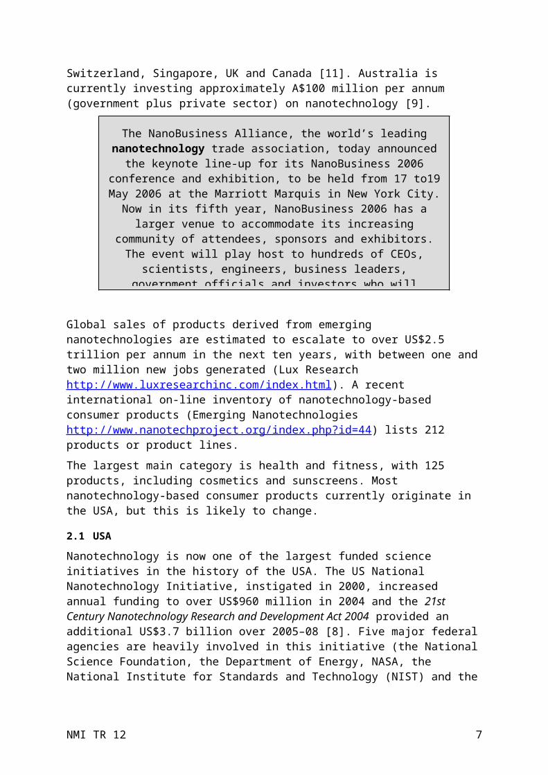
A world ranking of nations in nanotechnology places the current industrial leaders as USA, Japan, South Korea and a European Union block comprising Germany, France, Netherlands and Belgium. China, India, Brazil and perhaps Russia are poised to challenge for leadership over the next 10 to 15 years, while Australia falls into a group of smaller industrial nations that include Taiwan, Israel, Italy, Switzerland, Singapore, UK and Canada [11]. Australia is currently investing approximately A$100 million per annum (government plus private sector) on nanotechnology [9].
NMI TR 12 4

The NanoBusiness Alliance, the world’s leading nanotechnology trade association, today announced the keynote line-up for its NanoBusiness
2006 conference and exhibition, to be held from 17 to19 May 2006 at the Marriott Marquis in New York City. Now in its fifth year, NanoBusiness
2006 has a larger venue to accommodate its increasing community of attendees, sponsors and exhibitors. The event will play host to hundreds of
CEOs, scientists, engineers, business leaders, government officials and investors who will participate in three intensive days of seminars,
presentations and networking events. In addition, NanoBusiness 2006 will feature keynote presentations by some of the leading practitioners and
thinkers in nanotechnology.
Business Wire, New York, 28 March 2006
Global sales of products derived from emerging nanotechnologies are estimated to escalate to over US$2.5 trillion per annum in the next ten years, with between one and two million new jobs generated (Lux Research http://www.luxresearchinc.com/index.html). A recent international on-line inventory of nanotechnology-based consumer products (Emerging Nanotechnologies http://www.nanotechproject.org/index.php?id=44) lists 212 products or product lines.
The largest main category is health and fitness, with 125 products, including cosmetics and sunscreens. Most nanotechnology-based consumer products currently originate in the USA, but this is likely to change.
2.1 USANanotechnology is now one of the largest funded science initiatives in the history of the USA. The US National Nanotechnology Initiative, instigated in 2000, increased annual funding to over US$960 million in 2004 and the 21st Century Nanotechnology Research and Development Act 2004 provided an additional US$3.7 billion over 2005–08 [8]. Five major federal agencies are heavily involved in this initiative (the National Science Foundation, the Department of Energy, NASA, the National Institute for Standards and Technology (NIST) and the US Environmental Protection Agency), with investments distributed across seven major subject areas.
Significantly, NIST is one of these key agencies and a major subject area, instrumentation research, metrology and standards for nanotechnology, will receive US$75 million from the US$1.05 billion 2006 US National Nanotechnology Initiative budget. Despite this enormous investment in nanotechnology research and development, there are serious concerns that its leadership position is under threat [12].
Currently there is a bill before congress, the Nanoscience to Commercialisation Institutes Act 2006, to authorise grants to establish up to eight nanoscience to commercialisation institutes to develop commercial applications for nanotechnology.
2.2 CanadaCanadian governments, institutions, businesses and non-government organisations have been involved in nanotechnology for five years. 130 bodies have been identified with nanotechnology with the major centres being in Montreal (40%) and Toronto (25%). The work covers IT, medical, material science, aerospace, energy, automotive and the research
NMI TR 12 5
and service sectors. There are also industry associations, clubs, venture capitalists, nanoethics hubs and 25 university research centres. Governments have created centres of excellence at a number of universities and free-standing institutions. The national research funding bodies in medicine, science and engineering have funded numerous centres in research and product development. Workshops have been held in material science research and bioethics of nanotechnology. A national trade body boasts 1100 members and many businesses have products in the marketplace involving nanomaterials.
2.3 Asia–PacificJapan has been investing in nanotechnology since the 1980s but was spurred into further action in 2000 by the US National Nanotechnology Initiative. The Japanese Government set up the Expert Group on Nanotechnology, under the Japan Federation of Economic Organisations (Keidanren) Committee on Industrial Technology. Nanotechnology is now the key priority under Japan’s Science and Technology second basic plan and about US$1 billion is spent annually.
The Japanese Government views the successful development of nanotechnology as one of the keys to the reinvigoration and sustainable success of the Japanese economy. Government agencies and large corporations are the main sources of funding for nanotechnology in Japan; small and medium-sized companies play only a minor role. Research activities are generally grouped in relatively large industrial, government and academic laboratories.
South Korea has embarked upon a ten-year program involving US$2 billion of public funding [13] with the focus being on research and development, education and infrastructure.
Taiwan has a National Nanotechnology Program that coordinates research efforts from various government organisations. This program, launched in 2003 and scheduled to continue until 2008, has approximately US$700 million committed to four subprograms: industrial (61% of funding), academic excellence (21%), core facilities (16%) and education (1.3%). The industrial program is led by the Industrial Technology Research Institute, Taiwan’s dominant government research and development organisation. This program is further divided into nanoelectronics, nanomaterials, process and equipment development, and biomedical applications. The Nanotechnology Research Centre in Hsinchu, established in 2002, is the centre of the Industrial Technology Research Institute’s nanotechnology program. It contains an extensive array of characterisation, fabrication and measurement equipment.
The Taiwan Environmental Protection Administration has also commissioned projects related to nanotechnology research. This work includes the construction of an Internet databank on environmental applications such as air pollution control, waster water treatment, soil and ground water pollution treatment, environmental impacts and health risks of nanotechnology, and sensing technology. Another project concentrates on topics of environmental and health impacts of nanoparticles and nanomaterials, and emergency prevention.
China is devoting increasing resources to nanotechnology and is rapidly catching up with the European Union and the USA. In 1999, China began an ongoing nanomaterial and nanostructure project, providing support for basic research in nanomaterials, nanodevices, nanobiology and medicine, and detection and characterisation. A National Steering Committee for Nanoscience and Nanotechnology provides planning, coordination and consultation for projects at national level and has members from all of the ministries as well as leading scientists.
NMI TR 12 6

The markets in China for nanotechnology products and systems was US$4 billion in 2005 and is expected to increase to US$31.4 billion by 2010 and US$144.9 billion by 2015. Activity is concentrated on nanomaterials, nanoelectronics, nanobiosciences and nanolifesciences. World market share is expected to be more then 6% by 2010 and 16% by 2015. China is now one of the world leaders in terms of its number of newly registered nanotechnology firms, nanotechnology publications and nanotech related patents. Over the past three years, the number of companies in the field of nanotechnology in China has grown to over 800.
2.4 EuropeThe European Commission [14, 15] has adopted an action plan Nanosciences and Nanotechnologies: An Action Plan for Europe 2005–2009 [16]. This plan defines a series of actions for the implementation of a safe, integrated and responsible strategy for nanosciences and nanotechnologies. The plan is based on priority areas identified in Towards a European Strategy for Nanotechnology [15]. The Sixth EU Framework Programme for Research and Technological Development (FP6) has nanotechnology as one of its seven main programs. This program, Nanotechnology and Nanosciences, Knowledge-based Multifunctional Materials and New Production Processes and Devices, has a budget of €1,300 million for 2002–06. The European Union’s 7th Research Framework Programme has a theme on the development of nanotechnologies and nanoscale materials, which will also cover issues of associated environmental and human health and safety.
In the UK, the Department of Trade and Industry has recently launched the Micro and Nanotechnology Manufacturing Initiative (http://www.dti.gov.uk/innovation/micro-and-nanotechnology/index.html) with a budget of more than £90 million. The London Centre for Nanotechnology has been designed to act as a focus for current interdisciplinary nanoscale materials and device research. A joint enterprise with Imperial College London, the Centre will be housed in a new building offering eight levels of laboratory and office space for academics from electrical engineering, physics, chemistry, biology and medicine. Key infrastructure is to include a 200 m2 clean room and a complete range of nanocharacterisation facilities. The Interdisciplinary Research Collaboration in Nanotechnology is a collaboration between the University of Cambridge, University College London and the University of Bristol.
In Germany about €120 million is provided by the Federal Ministry of Research and Education for nanotechnology programs. Six competence centres have been established to improve the organisational infrastructure and to optimise the conditions for bringing potential users and nanotechnology researchers together. Nearly all German universities with a technical and scientific program of study are conducting nanotechnology research and development. Institutional research outside the universities is pursued by four large research associations: the Max Planck Society, the Fraunhofer Society, the Helmholtz Association of National Research Centres and the GW Leibniz Science Association. The players in the nanotechnology field in Germany include several hundred industrial companies. These comprise many large corporations such as Infineon, DaimlerChrysler, Schott, Carl Zeiss, Siemens, Osram, Degussa, BASF, Bayer, Metallgesellschaft and Henkel but also numerous small and mid-sized enterprises that are mainly concerned with production, analysis and equipment-related technologies in niche markets.
NMI TR 12 7

2.5 AustraliaAustralian nanotechnology is at a critical point (11), with the country poised to accept nanotechnology as an important part of its economy and well-being. The A$100 million annual investment in nanotechnology in Australia is comparable to Europe on a per capita basis. A recent government report [17] on future productivity in Australia concluded that:
One of the main sources of productivity growth will be technological progress in ICT and to a lesser extent biotechnology and nanotechnology … Nanotechnology is another general purpose technology with many promising applications. Its main impact will be on manufacturing, particularly the production of ICT equipment, MEMS, materials for drug delivery and materials with unique properties. Over 15% of [Australia’s] manufacturing output might incorporate some nanomaterials by 2020.
Both the Australian and State Governments have initiatives and strategies involving nanotechnology. The Department of Industry, Tourism and Resources recently announced the formation of the National Nanotechnology Strategy Taskforce (http://www.industry.gov.au/content/itrinternet/cmscontent.cfm?objectid=E2FE4F8A-4E44-4785-A6A01BE137E0E524&searchID=66684) to develop a national strategy on nanotechnology.
The Strategy will look at issues such as science capacity, industry development, health, safety and environment, metrology and standards, infrastructure and public engagement. The Taskforce is working with other government portfolios and with the States and Territories to develop a Strategy by June 2006. A key theme of the Strategy will be to ensure that Australia engages in international studies and activities designed to support the development of nanotechnology.
At the State level, a report on the Australian scene in nanotechnology [18] concluded that:
The two states which give the strongest support (to nanotechnology) are Queensland and Victoria. NSW has more limited activity in the area, as do South Australia and Western Australia.
Queensland in 2001/2002 earmarked A$63 million for stimulating innovation, particularly in advanced technology areas. Of the six projects which were funded, two were on nanotechnology. The University of Queensland, with the support of the State Government, has established the A$50 million Australian Institute of Bioengineering and Nanotechnology.
Victoria has a strong concentration of activities in nanotechnology … The strong medical and biotechnology research and commercialisation activities provide the opportunity for strong interaction in the nanobiotechnology area. The Victorian Government has awarded A$12 million over 3 years … to support the setting-up of Nanotechnology Victoria (Nanovic http://www.nanovic.com.au/?referrer=AZoNanoBanner) which draws together most of the major research and development groups of universities and of CSIRO in Victoria in a unified approach.
There are a number of activities in the other states, including: Centre for Quantum Computer Technology at the University of NSW; Institute for Nanoscale Technology at the University of Sydney; A$200 million Electron Science Valley near Perth; and
NMI TR 12 8

active groups in sensors, microchips, nanocomposites and nanomaterials at Flinders University and the Ian Wark Institute in South Australia.
The result of this support is that basically nanotechnology research and development in Australia is strong. Over 2500 nanoscience papers were produced in 1998–2003 (1.5% of global papers), with a high citation rate (11 versus 8 average) and high collaboration (45% international versus 35% all science). These papers focused on nanomaterials (50%) and nanobiotech (25%). Australia was ninth in the world in foreign-sourced US patents involving nanotechnology (11).
Most funding is provided by the Australian Government through: the Australian Research Council, the National Health and Medical Research Council, CSIRO, the Cooperative Research Centres Program, the Defence Science and Technology Organisation, and the Australian Nuclear Science and Technology Organisation.
Several research networks have been established, including the Australian Research Council Nanotechnology Network (http://www.ausnano.net/), the Nanostructural Analysis Network Organisation (http://www.nano.org.au/index.htm) and OzNano2Life, a network of key Australian scientists and research institutions, whose research is in the area of nanobiotechnology. The major purpose of OzNano2Life is to provide the portal for structured exchange of scientists and information with European nanotechnology institutes. The objective is to facilitate ongoing collaboration in nanobiotechnology research.
The level of activity in Australian business and industry is small but steadily growing. There are at least 50 companies with an involvement in nanotechnology covering activities ranging from new materials and particles to medical and pharmaceuticals devices. A business network, the Australian NanoBusiness Alliance (http://www.nanobusiness.org.au/) has recently formed.
The PMSEIC Report [9] noted that there are five industry sectors where Australia has significant nanotechnology opportunities based on the improvements available through current technology developments. These are: minerals and agribusinesses; medical devices and health; energy and environment; advanced materials and manufacturing; electronics and information and communications technologies.
A survey of companies [19] likely to have an interest in nanotechnology from the manufacturing, materials, automotive, ICT/electronics, textiles and biotechnology industries was conducted in August 2005 by Nanovic and the Department of Industry, Tourism and Resources. Among those surveyed, awareness of nanotechnology was high with 20% already investing in nanotechnology and 70% expecting revenue from nanotechnology in the next 5 years. Companies that have not yet made investments in nanotechnology expect to be making critical decisions about investments in the next five years. Businesses do not perceive strong barriers to investing in nanotechnology and government is seen as having an important role to play in the nanotechnology industry, particularly in the regulatory arena.
A gross impact initial assessment of the economic impacts of nanotechnology in Australia may be obtained by proportioning global estimates of the value of goods and services incorporating nanotechnology against Australia’s share of global gross domestic product. This gives a figure of A$20.5 billion by the year 2015. This is an indicator only but it does give an idea of the magnitude of goods and services that are likely to be affected.
The significance of nanotechnology to the Australian economy is apparent but it goes beyond opportunities for new markets and added wealth. Nanotechnology has the potential to be an important solution to serious structural problems facing Australian industry at present,
NMI TR 12 9
particularly in the manufacturing sector, due to the emerging capability of China, India and other large, low-wage economies.
The emergence of these economies operating across the value chain coupled with increasing free trade activities will require Australia to redirect investment into the upper end of the value chain. Australian industry will need to become more specialised around areas of comparative advantage.
The manufacture of higher-value added products will demand an increase in research and development, particularly at the middle or upper sections of the value chain. However, the current situation in Australia sees relatively low business investment in manufacturing, turnover concentrated on capital-intensive production and very low levels of research and development expenditure focussed on the lower value-added activities.
Nanotechnology requires long-term, strategic research and development, innovation and interdisciplinary and collaborative work. It offers Australian industry an opportunity to move up the value chain and remain viable in an increasingly competitive world.
Nanotechnologies, the German nanotechnology company, has brought a temporary injunction against Norddeutsche Rundfunk, the German publicly-owned regional
broadcaster. A court has forbidden the TV broadcaster to indicate that the nanotechnology company markets food additives with false information. The
broadcasting company has also been forbidden to continue to report that the products do not contain nanoparticles of between 3 and 10 nm.
Financial Times Deutschland, 2006 — Neosino
3. NANOPARTICLE ACTIVITY IN AUSTRALIANanoparticles are defined as particles with one or more dimensions of the order of 100 nm or less [20]. Nanoparticles are often said to exhibit new or enhanced size-dependent properties compared with larger particles of the same material. This difference in properties is usually due to an increased relative surface area or a dominance of quantum effects [2].
Nanoparticles exist widely in the natural world: for example as the products of photochemical and volcanic activity and created by plants and algae. They have been around for thousands of years as products of combustion and food cooking, and more recently from vehicle exhausts.
Internationally, research and development into nanoparticles has the highest levels of investment and most nanotechnology products on the market today involve nanoparticles. Industries involving nanoparticles are extremely varied and may be divided into three categories, namely: biomedical, pharmaceutical and cosmetic applications; energy, catalytic and structural applications; and electronics and photonics.
Manufactured nanoparticles are often not products in their own right, but serve as raw materials, ingredients or additives in existing products. These include waterproof clothing, chemical-mechanical polishing, magnetic recording tapes, sunscreens, cosmetics, fuel additives, inks for ink-jet printers, precursor powders for materials manufacture, biolabelling, electro-conductive coatings and optical fibres.
The accelerating production, experimentation and use of nanoparticulate materials, along with the requirements for new handling and measurement technologies, is leading to growing
NMI TR 12 10

concerns on health and safety issues for industrial uses and environmentally derived sources (see below).
3.1 Commercial ActivityRecent surveys [21, 22] list 13 companies involved with manufacturing nanoparticles or nanopowders. These are located in New South Wales (5), Victoria (3), Queensland (3), Western Australia (1) and South Australia (1). See also Appendix A.
Six of these companies manufacture nanoparticles, three incorporate nanoparticles into commercial products, three encapsulate chemicals and pharmaceuticals into nanoparticles and one supplies nanoparticle equipment and instrumentation. Nanoproducts made in Australia include cosmetics and sunscreens, ultra-violet resistant coatings on bottles, stain-resistant and wrinkle-free textiles and nucleating agents.
Interviews were conducted with representatives from two major companies, Advanced Nanotechnology Ltd and Micronisers Ltd. In addition, discussions were held with a variety of other companies, industry representatives and state government organisations.
The main points to emerge from these contacts were:
Commercial activity in nanotechnology in Australia is similar to the international situation, in that products and processes involving nanoparticles dominate.
While the number of nanoparticle companies and their economic significance is relatively low, these companies are optimistic and forecast growth. Many of them have already established an export market and are expanding their operations.
Competition in nanoparticle production from the Asia–Pacific is increasing, particularly from China.
Traceability and international acceptance of measurement are not issues at present, but it is anticipated that these will become more important as export markets increase and clients become more astute.
Most nanoparticle companies recognise the importance of measurement in their operations.
Numerous measurands are used for characterising nanoparticles and many of the measurable parameters may be determined by more than one technique. These techniques can be based on fundamentally different processes, requiring differing degrees of interpretation and often leading to different results.
There is a need for fast and accurate measurement capability for use in the production process.
Regulatory issues concern many companies and there is a strong desire for guidance in the regulation of nanoparticles.
The small number of commercial nanoparticle companies does not allow firm conclusions to be made concerning any national concentrations of industries.
3.2 ResearchSurveys of research institutions in Australia [21, 23] list 17 institutions with involvement in nanoparticles or with a nanoparticle capability. These are located mainly in NSW, Victoria and Queensland. Many research institutions belong to national networks, such as NANO
NMI TR 12 11

(http://www.nano.org.au/index.htm) and Nanotechnology Network (http://www.ausnano.net/index.php?page=home). See also Appendix B.
NMI TR 12 12

The main points to emerge from contacts with the research institutions were: Australia has a substantial research base, although small by global standards; research is sustained by public investment, which accounts for well over half of
Australia’s estimated total investment of around A$100 million per annum; they have a considerable level of expertise and extensive facilities in nanoparticle
measurement and they are engaged in a wide range of research topics; they are generally uninformed about measurement traceability and the role of NMI; they have problems with the reproducibility and accuracy of their measurements; and they are eager to engage with NMI and to try and resolve their measurement problems.
4. NANOMETROLOGY
Nanometrology is essentially an enabling technology. Nanotechnologies, however defined, cannot progress independently of progress in nanometrology. Apart from their direct
influence on scientific research and its application, the solutions developed for nanometrology problems can often be exploited elsewhere [2].
Nanometrology, the science of measurement at the nanoscale, underpins all nanoscience and nanotechnology. This is clearly recognised by governments, research institutions and the private sector throughout the world. The US National Nanotechnology Initiative established instrumentation research, metrology and standards for nanotechnology as one of its seven major activities because ‘it is the crucial step to commercialising nanotechnology’ [8]. The aim is to advance the boundaries of knowledge in instrumentation and metrology and to bring state-of-the-art tools and techniques to bear in the development of standards for the nanotechnology community.
When you can measure what you are speaking about, you know something about it. But when you cannot measure it, your knowledge is of a meagre and unsatisfactory kind. It may be the beginning of knowledge, but you have scarcely
advanced to the stage of science.
William Thomson, Lord Kelvin 1883
The European Commission [15] stated that:
To ensure that the European Union can realise the commercial potential of nanotechnology, industry and society will require reliable and quantitative means of characterisation as well as measurement techniques that will underpin the competitiveness and reliability of future products and services. Metrology and standards need to be developed to facilitate rapid development of the technology as well as providing users with the necessary confidence in their process and product
NMI TR 12 13

performance. Innovative developments in measurement techniques are needed to cope with the demands of nanotechnology.
This is a challenging area of activity. At the nanoscale, it becomes difficult to disentangle the perturbing effects of measuring instruments on the measurement itself. In certain areas, metrology tools are simply not available at present. Considerable pre-normative research and development are required, taking into account the needs of industry in terms of rapid measurement, and control.
The Royal Society Report [2] concluded that:
Metrology, the science of measurement, underpins all other nanoscience and nanotechnologies because it allows the characterisation of materials in terms of dimensions but also in terms of attributes such as electrical properties and mass. Greater precision in metrology will assist the development of nanoscience and nanotechnologies.
Similarly, Australia’s PMSEIC Report [9] recognised that:
… nanometrology underpins the ability to attract international investment and partnerships and helps eliminate technical barriers to trade and underpins regulatory frameworks.
4.1 Nanometrology InfrastructureThe establishment of a nanometrology infrastructure in Australia is a prerequisite for regulations and standards for nanoparticles and for nanotechnology to reach its full potential.
Responsibility for the provision of such an infrastructure clearly lies with NMI, whose prime directives include providing the legal and technical framework for disseminating measurement standards, working with clients in industry and government to provide measurement expertise, calibration services and analytical testing, and supporting the broader standards and conformance infrastructure.
The commencement of a substantial nanometrology program within NMI is the most appropriate way to proceed. The first stage should be the establishment of physical standards and their dissemination via a calibration service. Coupled with high-level research and development, and national and international comparisons, this would lead to both a growth of the local measurement skills necessary to sustain Australian nanotechnology and enhance Australia’s international reputation. Clause 6 is a survey of nanometrology methods and instruments, concentrating on dimensional nanoscale and nanoparticle metrology.
Creating standards and traceability for dimensional nanoscale metrology is a fundamental step in establishing a metrological infrastructure for nanotechnology.
Traceability [31] is ‘the property of the result of a measurement or the value of a standard whereby it can be related to stated references, usually national or international standards, through an unbroken chain of comparisons all having stated uncertainties.’
Traceability for dimensional nanoscale metrology consists essentially of transferring the realisation of the primary standard for the metre down to measurements at the nanometre level via a chain of instruments and comparisons. The quality of this process is ensured using international comparisons and continuous research and development.
The SI definition of the metre is the length of the path traveled by light in vacuum during a time interval of 1/299 792 458 of a second. This is realised practically in Australia using the accurately known optical wavelengths of light generated by three iodine-stabilised helium
NMI TR 12 14

neon lasers. Traceability for length measurements in Australia is achieved by using these lasers to calibrate the frequencies of lasers used in high-level length measuring instruments or to directly measure the length of material artefacts by interferometry.
Establishing traceability for nanoscale measurements requires first a way of visualising the nanoworld, adding a length measuring system to this visualisation system and then calibrating this length scale against the primary standard lasers.
4.2 Development of Standards and RegulationsA common concern is the need for guidance, information, standards and regulation on nanoproducts, particularly those involving nanoparticles. These concerns are a subset of a broader debate on the Ethical, Economic, Environmental, Legal and Social Issues (NE3LS) of Nanotechnology [24]. This level of public debate on the social issues surrounding nanotechnology is unusual for a technology at only the very earliest stages of its development [25–30].
The development of products using technology that manipulates matter at the atomic and molecular scales has raised concerns about the safety of the workers who manufacture them. The Washington Post reports that federal regulators are claiming they need more data before they can set safety standards for the nanotechnology industry. There are currently no state or federal rules addressing the risks of working with nanomaterials, even though several studies with animals have shown that exposure to certain types of
chemical reactions involving nanoparticles can be dangerous. ‘We have very little data to make any kind of informed societal decisions about how to deal with nanomaterials in the workplace,’ said Paul Schulte, the Director of Education and Information at the National
Institute for Occupational Safety and Health. Alan Gotcher, the Chief Executive of Altair, said nanotech companies need to move quickly on the issue.
Worker Safety in Nanotech Industry is a Concern, Technology Daily AM, 10 April 2006
Nanoparticles occur in the natural world and people have always been exposed to them. Engineered nanoparticles, however, are the end products of a wide variety of physical, chemical and biological processes some which are novel and radically different, others which are quite commonplace. Little is known about exposure to these nanoparticles by inhalation, ingestion or via the skin, and there are major gaps in the knowledge necessary for risk assessments. These include nanoparticle characterisation, the detection and measurement of nanoparticles, the dose-response, fate and persistence of nanoparticles in humans and in the environment, and all aspects of toxicology related to nanoparticles.
The main technical challenges associated with exposure to nanoparticles [2] are:
Geometry — measuring irregularly shaped particles and tubes.
Simultaneous measurement of different metrics — can information about size, surface area, chemical species etc be measured at the same time?
Specificity — the ability to differentiate (and quantify) particles of interest from the background.
Portability and robustness — can the apparatus be used in workplaces?
NMI TR 12 15

Validity — are the results of measurements a valid representation of the exposure conditions?
NMI TR 12 16

German officials have reported what is possibly the first health-related recall of a nanotechnology product, The Washington Post reports. The field of nanotechnology, or the manipulation of matter at the atomic and molecular scales, is quickly growing
but remains poorly understood. At least 77 people reported severe respiratory problems and some were hospitalised for fluid in the lungs over a one-week period at the end of March after they used a ‘Magic Nano’ bathroom cleansing product. ‘The distributors have launched a recall and advised against using the sprays,’ said the
Federal Institute for Risk Assessment in Berlin. ‘This really raises a bunch of interesting questions since the public has been told that nano will cure diseases, not
cause them,’ said David Rejeski, Director of the Project on Emerging Nanotechnologies at the Woodrow Wilson International Centre for Scholars in
Washington. ‘I think this is an important event in the nano world.’
The UK report [2] concluded:
There is a need to develop agreed standards that can be used to calibrate equipment that will be used by both industry and regulators.’ and ‘In addition to the development of measurement techniques for regulatory purposes, there is a growing need for international measurement standards for nanoscalar metrics. These will include but not be limited to dimension, chemical composition, force and electrical quanta. Monitoring of nanoparticles in the workplace will also require a high level of traceability to ensure that any future agreed exposure levels are accurately adhered to.
As well as protecting society and the environment, standardisation promotes public acceptance and aids growth in productivity by supporting innovation, value generation and compliance. The production of well characterised and controlled nanotechnology-applied products depends on the availability of documentary standards for terminology and nomenclature and measurement and characterisation.
The International Organisation for Standardization has recently convened a new committee to examine this area, TC229 Nanotechnologies, which met for the first time in London in November 2005. Standards Australia represented Australia at this meeting. The scope of this committee is standardisation in the field of nanotechnologies that includes either or both of the following:
understanding and control of matter and processes at the nanoscale, typically, but not exclusively, below 100 nm in one or more dimensions where the onset of size dependent phenomena usually enables novel applications; and
utilising the properties of nanoscale materials that differ from the properties of individual atoms, molecules and bulk matter, to create improved materials, devices and systems that exploit these new properties
Specific tasks include developing standards for: terminology and nomenclature; metrology and instrumentation, including specifications for reference materials; test methodologies; modelling and simulation; and science-based health, safety and environmental practices.
Three working groups were established for TC229: WG 1: Terminology and Nomenclature, convened by Canada; WG 2: Measurement and Characterisation, convened by Japan; and WG 3: Health, Safety and Environmental Aspects of Nanotechnologies, convened by
the USA.
NMI TR 12 17

In March 2006, Standards Australia established NT-001 Nanotechnologies, a committee that has the same scope and working group structure as TC229. This committee will coordinate Australia’s contributions to TC229 and eventually produce Australian standards for nanotechnology. The committee includes representatives from: Standards Australia; National Association of Testing Authorities; National Industrial Chemicals Notification and Assessment Scheme; Australian Council of Trade Unions; Plastics and Chemicals Industry Association; Science Industry Australia; Australian Research Council Nanotechnology Network; Australian Academy of Technological Sciences and Engineering; CSIRO; and NMI.
NMI’s representative is the chair of the committee, primarily due to NMI’s independence.
The development of a regulatory framework in Australia for nanotechnology requires consultation and coordination between Australian Government portfolios and agencies and state authorities. The organisations with most responsibility in this area are the Australian Safety and Compensation Council, the National Industrial Chemicals Notification and Assessment Scheme and the Therapeutic Goods Administration.
The National Nanotechnology Strategy taskforce has recently convened an Environment, Health and Safety Subgroup to progress incorporation of environmental, health and safety issues into the proposed national nanotechnology strategy. This group includes representatives from the Australian Safety and Compensation Council, the National Industrial Chemicals Notification and Assessment Scheme and the Therapeutic Goods Administration as well as Food Standards Australia New Zealand, the Department of the Environment and Heritage and the Department of Transport and Regional Services. NMI is also represented in this group.
5. NANOMETROLOGY METHODS AND INSTRUMENTSThe two most common instruments used to visualise the nanoworld are the electron microscope (EM) and the scanning probe microscope (SPM).
5.1 Electron MicroscopyEMs use electrons as illumination rather than visible light. This is because the maximum resolution (ability to discriminate features) of a microscope is approximately equal to the wavelength of the illumination used. This is 300 to 600 nm for visible light but for electrons the wavelength, and hence the potential resolution, is 0.002 to 0.1 nm depending on the electron energy.
The transmission electron microscope (TEM) involves a high voltage electron beam emitted by a cathode and shaped by magnetic lenses. The electron beam is partially transmitted through a very thin specimen and carries information about the inner structure of the specimen. The spatial variation in this information (the ‘image’) is then magnified by a series of magnetic lenses until it is recorded by hitting a fluorescent screen, photographic plate, or light sensitive sensor such as a CCD (charge-coupled device) camera. The image detected by the CCD may be displayed in real-time on a monitor or computer.
NMI TR 12 18

The actual resolution achieved by a TEM is limited by spherical and chromatic aberration, but recently a new generation of TEMs has overcome spherical aberration, allowing the production of images with sufficient resolution to show carbon atoms in diamond separated by only 0.089 nm and atoms in silicon at 0.078 nm at magnifications of 50 million times. The ability to determine the positions of atoms within materials has made these high resolution TEMs an indispensable tool for nanotechnology research and development in many fields.
Unlike the TEM, where electrons are detected by beam transmission, the scanning electron microscope (SEM) produces images of surface features by detecting secondary electrons emitted from the surface due to excitation by a primary electron beam. In the SEM, the fine primary electron beam is scanned across the sample, with detectors building up an image by mapping the detected signals with beam position.
Generally, the TEM resolution is about an order of magnitude better than the SEM resolution. However, because the SEM image relies on surface processes rather than transmission it is able to image bulk samples and has a much greater depth of view, and so can produce images that are a good representation of the three-dimensional structure of the sample. A scanning transmission EM is a specific sort of TEM, where the electrons still pass through the specimen, but, as in SEM, the sample is scanned in a raster fashion.
5.2 Scanning Probe MicroscopyScanning probe microscopy is a branch of microscopy founded with the invention of the scanning tunnelling microscope. A fine probe is scanned across a surface. The probe position above, or on, the surface is controlled by a feedback signal. The same signal is used to provide image contrast on an associated display.
The feedback signal for the scanning tunnelling microscope is the electron tunnelling current between the conducting specimen and probe suspended a few tenths of a nanometre above its surface. The atomic force microscope (AFM) uses the Van der Waals forces between the specimen and the probe. The use of further feedback mechanisms has led to a number of SPM imaging methods, including magnetic force microscopy, lateral force microscopy, shear force microscopy and near field scanning optical microscopy. All methods can be operated in a range of environments, including atmospheric conditions, liquid immersion and vacuum.
NMI TR 12
Commercial SEM
SEM image of single wall carbon nanotube
19

The advantage of the SPM is that the resolution is not limited by diffraction, but only by the size of the probe-sample interaction volume, which can be as small as a few picometres. The SPM can also be used to modify the sample to create small structures. The disadvantage is that the scanning technique is generally slow in acquiring images and the maximum image size is small.
The AFM is the most commonly used SPM for nanometrology. The probe is on the end of a flexible beam or cantilever whose displacement is measured using a laser beam. The AFM is not limited to conductive surfaces as it is for scanning tunnelling microscopes. The AFM has several advantages over the EM. Samples viewed by an EM require special treatment that is often destructive and need an expensive vacuum environment for proper operation. AFMs work perfectly well in an ambient or even liquid environment.
The main disadvantage of the AFM is the image size. The SEM can show an area on the order of millimetres by millimetres and a depth of field on the order of millimetres. The AFM can only show a maximum height of the order of micrometres and a maximum area of around 150 by 150 m. Additionally, the AFM cannot scan images as fast as an SEM. It may take several minutes for a typical region to be scanned with the AFM, however an SEM is capable of scanning at near real-time.
NMI TR 12
Principle of AFMAtomic lattice using an AFM
AFM tip
Calibration grating for AFM
20
5.3 Adding a Length ScaleQuantitative length measurements using an SEM or an SPM require the addition of a length measuring system fitted directly to the scanning system. These are typically strain gauges, capacitive or inductive sensors, optical encoders etc. These length measuring systems are calibrated using gratings, grids or steps with microstructures of defined geometry. A traceable calibration may also be achieved by imaging the atomic lattice planes of materials with known lattice spacing. However, this has limited value due to the non-linearity in the magnifications of SEMs and SPMs. The problem then reduces to the provision of traceable calibrations of microstructures of defined geometry, such as gratings, grids or steps, which are then used to calibrate SPMs and SEMs/TEMs.
5.4 Traceability for Nanoscale MeasurementsOne-dimensional reference gratings with a pitch between a few hundreds of nanometres and tens of micrometres may be calibrated using optical diffractometry. Both gratings and grids may be calibrated using SPMs or SEMs equipped with laser interferometers on the x–y positioning axes, allowing positions to be accurately and continuously traced back to the wavelength of the laser light and hence to the metre [32]. These instruments are known as metrological SPMs or SEMs. Instruments and techniques for extending the accuracy and range of metrological SPMs (in particular) and SEMs are currently being developed in many national metrology institutes.
At the sub-nanometre level, nonlinearities in optical interferometry begin to appear. This has led to the use of X-ray interferometry. The fringe spacing in X-ray interferometers is independent of the wavelength of the incident radiation, being determined by the spacing of the diffraction planes in the crystal from which the X-rays are diffracted, normally silicon. There has been significant work over the last ten years in establishing traceability to the metre for the spacing of the lattice planes of silicon, driven mainly by the Avogadro project. A notable instrument developed by several national metrology institutes is the combined optical and X-ray interferometer, in which displacement may be measured simultaneously using an optical interferometer and an X-ray interferometer. This instrument is capable of picometre uncertainties for length measurements.
Traceability for nanometrology measurements in the z-direction requires step height artifacts. Step height measurement at the nanometre level may be achieved using a metrological SPM with a laser interferometer fitted to the z-axis. A stylus instrument, in which a sharp stylus is placed in contact with the surface and scanned over it, may also be used but it needs to be provided with its own traceable calibration. An interference microscope is also commonly used.
The distinctive feature of an interference microscope is that the illuminating light beam, as in interferometers, is split into two beams that travel along physically separated paths before being recombined and interfering with each other. As with an interferometer, observing and quantifying the interference effect permits the optical path difference between the two beams to be measured. This is then used to calculate the step height in terms of the optical wavelength.
The ellipsometer is used to measure the thickness of semi-transparent thin films. This instrument relies on the fact that the reflection at a dielectric interface depends on the polarisation of the light while the transmission of light through a transparent layer changes the phase of the incoming wave depending on the refractive index of the material. An ellipsometer can be used to measure layers as thin as 1 nm up to layers that are several microns thick. Applications include the accurate thickness measurement of thin films, the identification of materials and thin layers and the characterisation of surfaces.
NMI TR 12 21
A recent development in nanometrology instrumentation is the micro-Coordinate Measuring Machine (µ-CMM). These are based on conventional CMMs, operating over much smaller measuring volumes (10 µm3 to 50 mm3) with a correspondingly lower measurement uncertainty (50 nm to 1 µm). They are designed for objects too small for conventional CMMs to probe safely and too large for standard nanometrology instruments (AFMs etc). Countries that have developed (or are developing) µ-CMMs include the UK, USA, Germany, Switzerland, Japan and the Netherlands. There has been mention recently of the development of a µ-CMM by a European consortium of instrument manufacturers and national metrology institutes.
5.5 Nanoparticle Measuring InstrumentsParticle size measurement is characterised by a variety of instruments, a variety of parameters and a variety of testing conditions all with different regions of applicability. Australia is a world leader in particle size research and development with a long and distinguished history. Methods for diameter measurement include: dry sieve 1 mm–10 µm wet sieve 1 mm–1 µm gravitational sedimentation 500 µm–1 µm light microscopy 500 µm–1 µm electrical sensing zone 500 µm–0.5 µm capillary chromatography 100 µm–0.5 µm light scattering 100 µm–100 nm surface area 100 µm–80 nm centrifugal sedimentation 80 µm–80 nm dynamic light scattering 5 µm–3 nm electron microscopy 1000 nm–2 nm size exclusion chromatography 100 nm–10 nm field flow fractionation 100 nm–5 nm pulsed field gradient nuclear magnetic resonance 100 nm–1 nm small angle X-ray scattering 10 nm–0.1 nm atomic force microscopy 1000 nm–0.1 nm
NMI TR 12
µ-CMM at Switzerland’s national metrology institute
22

5.5.1 Dynamic Light ScatteringWhen a beam of light passes through a suspension, the particles or droplets scatter light in all directions. When the particles are very small compared with the wavelength of the light, the intensity of the scattered light is uniform in all directions (Rayleigh scattering); for larger particles (above approximately 250 nm diameter), the intensity is angle dependent (Mie scattering). If the light is coherent and monochromatic, as from a laser, it is possible to observe time-dependent fluctuations in the scattered intensity using a suitable detector such as a photomultiplier capable of operating in photon counting mode.
These fluctuations arise from the fact that the particles are small enough to undergo random thermal (Brownian) motion and the distance between them is therefore constantly varying. Constructive and destructive interference of light scattered by neighbouring particles within the illuminated zone gives rise to the intensity fluctuation at the detector that, as it arises from particle motion, contains information about this motion. Analysis of the time dependence of the intensity fluctuation yields the diffusion coefficient of the particles from which, using the Stokes-Einstein equation and knowing the viscosity of the medium, the hydrodynamic radius or diameter of the particles can be calculated.
The time dependence of the intensity fluctuation is most commonly analysed using a digital correlator. Such a device determines an intensity autocorrelation function which can be described as the ensemble average of the product of the signal with a delayed version of itself as a function of the delay time. The ‘signal’ in this case is the number of photons counted in one sampling interval. At short delay times, correlation is high and, over time as particles diffuse, correlation diminishes to zero and the exponential decay of the correlation function is characteristic of the diffusion coefficient of the particles. Data are typically collected over a delay range of 100 ns to several seconds depending upon the particle size and viscosity of the medium.
Analysis of the autocorrelation function in terms of particle size distribution is done by numerically fitting the data with calculations based on assumed distributions. A monodisperse sample would give rise to a single exponential decay to which fitting a calculated particle size distribution is relatively straightforward. In practice, polydisperse samples give rise to a series of exponentials and several quite complex schemes have been devised for the fitting process.
5.5.2 Electron MicroscopyNanoparticles may be imaged by both SEM and TEM. Conventional SEMs are typically capable of resolving details with a spatial resolution of 5 to 10 nm, although this figure becomes significantly poorer under less than ideal conditions. SEMs with bright and coherent Field Emission Electron Guns (FEG-SEM) are capable of a spatial resolution of 1 nm and below. While the conventional SEM requires the specimen to be held under a vacuum during analysis, environmental SEMs (ESEM) enable samples to be studied in a low pressure gaseous environment.
TEMs require thin electron-transparent samples and normally a higher level of sample preparation. However, nanoparticles are electron transparent in a single layer and this is relatively easy to achieve by spreading a dilute solution of the particles onto a grid and drying TEMs are routinely capable of achieving sub-nanometre spatial resolution, although the achievable resolution is dependent on the sample as well as the microscope being used. Electron beams smaller than 0.2 nm in diameter may be formed in high-resolution scanning transmission EMs, allowing sub-nanometre spatial resolution characterisation of particles.
NMI TR 12 23

5.5.3 Size Exclusion ChromatographyIn this technique, particle separation occurs in a column packed with a porous non-adsorbing material with pores of approximately the same size as the dimensions of the particles to be separated. A carrier liquid is passed through the column, with the larger particles exiting first because they are too large to get caught up in the pores. The smaller particles enter the pores and are retained according to the volume that can be accessed by the particle; the smaller particles having the longer the delay.5.5.4 Field Flow FractionationThis technique separates particles in suspension flowing along a channel by applying a force field perpendicular to the flow. The force field can be gravitational, thermal, magnetic or even another flowing liquid. Because the separation exposes the different sized particles to different flow velocities within the stream, the different sized particles arrive at the other end of the flow at different times. Field flow fractionation is the most accurate method below 50 nm.5.5.5 Pulsed Field Gradient Nuclear Magnetic ResonancePulsed-field gradient nuclear magnetic resonance provides a convenient and non-invasive means for measuring the translational motion of particles in suspension. The method uses normal nuclear magnetic resonance techniques to measure the displacement of the nuclear spins within the suspended particles. From this, a self-diffusion coefficient may be calculated and hence the particle radius.5.5.6 Small Angle X-ray ScatteringSmall angle X-ray scattering is an analytical X-ray application technique for the structural characterisation of solid and fluid materials in the nanometre range. The sample is irradiated by a monochromatic X-ray beam. When a non-homogeneous medium is irradiated, structural information of the scattering particles can be derived from the intensity distribution of the scattered beam at very low scattering angles. With small angle X-ray scattering it is possible to study both monodisperse and polydisperse systems. In the case of monodisperse systems one can determine size, shape and internal structure of the particles. For polydisperse systems a size distribution can be calculated under the assumption that all particles have the same shape.
Synchrotrons in the USA, Japan and Europe are often used to determine particle size using small angle X-ray scattering because of their very bright X-ray beams. One of the beam lines on the new Australian synchrotron will be an small angle X-ray scattering instrument and the new OPAL reactor will have a small angle neutron scattering instrument.5.5.7 Atomic Force MicroscopeAFMs are able to provide high-resolution images of nanoparticles. There are relatively few limitations on the type of sample imaged and the AFM has several advantages over electron microscopy methods, including rapid sample analysis, minimal sample preparation and analysis under ambient conditions.
5.6 Traceability of Nanoparticle Measuring InstrumentsTraceability is not well-established within the general particle measuring community, much less nanoparticles. For many of the instruments described above, standard reference materials (SRMs) in the form of powders are used to check instruments. These SRMs are certified for a particle size distribution but this may not be a formally traceable measurement. The traceable calibration of AFMs and SEMs has already been discussed (see clause 4.4).
NMI TR 12 24
6. NANOMETROLOGY — INTERNATIONAL ACTIVITIESAll major economic nations have a national metrology institute whose main role is to establish, maintain and disseminate physical standards of measurement. International comparisons and agreements between the more than 100 national metrology institutes establish international and national traceability of measurements, making measurements quantitatively comparable and enhancing trade. In response to improvements in science, technology and manufacturing processes, national metrology institutes continuously develop and improve standards to fulfil the needs of their national industry and society.
It is important to understand that the national metrology institutes in many of the larger economies, e.g. USA, UK, Germany and Japan, are large, broad-based research institutes with a wide range of nanotechnology activities and programs such as nanomaterials development, nanostructured surfaces, quantum computing, nanobiotechnology, nanoelectronics, nanofabrication, nanooptical technology, surface and nanoanalysis. This work needs to be distinguished from those nanometrology activities that are concerned with establishing a formal measurement infrastructure, although there is often overlap in terms of knowledge and expertise.
The following review of national metrology institutes concentrates on dimensional nanoscale and nanoparticle metrology. The very different nature of nanotechnology means that conventional standards, measurement methods and instrumentation are increasingly unable to provide the necessary measurement parameters, range, uncertainty and accuracy. Consequently, most national metrology institutes have invested significantly in establishing nanometrology laboratories and programs, several reaching the point where they are able to offer formal measurement services. These services include the measurement of surface features such as line widths and step heights using stylus-based optical and scanning probe microscopy, and the calibration of: SPMs using grating standards or by calibrating the positioning stage using
interferometry and nanometre displacement sensors; nanometre displacement transducers such as piezoelectric, capacitive or inductive
transducers; and masks used by the microelectronics industry.
Excellent reference sources include the proceedings from two major international symposiums on nanoscale calibration standards and methods [33, 34] and two reports on international comparisons which provide information on the capabilities and equipment in the participating institutes [35, 36].
6.1 National Institute of Science and Technology (USA)http://www.nist.gov/
Nanometrology is a subset of a very wide range of programs and scientific activities at NIST. As previously stated (see clauses 2.1 and 4), the US National Nanotechnology Initiative has established ‘instrumentation research, metrology and standards for nanotechnology’ as one of its seven major activities and NIST will receive US$75 million for nanotechnology in 2006, unchanged from 2005. Developments in measurements, standards and nanocharacterisation occur within broader programs.
NIST has a large range of collaborations with industry and a significant proportion of its budget is distributed to the private sector via industry grants or collaborations [37]. NIST plans to direct half of the new nanotechnology funding to external organisations to conduct much of the specific work required to meet the goals of this initiative and to avoid developing costly, complex in-house capabilities that may only be used once.
NMI TR 12 25
Due to the strength of the microelectronics industry in the USA, many of NIST’s existing activities involve nanoscale metrology of planar structures on semiconductors, masks, grids and scales, often referred to as critical dimension metrology. This is also true of countries such as Japan, Taiwan, Korea, Germany and the UK.NIST has indicated that new nanomanufacturing and nanofabrication programs will be inaugurated in 2006 to support research into nanoimprint lithography, particle metrology and other manufacturing metrology techniques. These programs also support development and delivery of measurement and infrastructure technologies to provide traceable metrology, process-control and quality assurance for nanoscale manufacturing. Funding will be increased for research on measurements of nanomechanical properties and on nanotube/nanoparticle metrology, and for efforts to produce nanoelectronics and nanophotonics devices.A very important initiative was the National Nanomanufacturing and Nanometrology Facility which opened in Gaithersburg in 2005. The facility supports the development of new infrastructural metrology and standards through centralised access to NIST’s nanometrology and nanofabrication resources, including the facilities of the Advanced Measurement Laboratory and NIST’s nanometrology experts.
Advanced Measurement Laboratory, NIST
The Advanced Measurement Laboratory is one of the world’s best research facilities, consisting of five wings, including two that are underground. The 50 000 m2 building houses 338 reconfigurable laboratory modules and a class 100/ISO 5 clean room. Environmental controls and design ensures strict temperature and humidity control, vibration isolation, air cleanliness and quality of electric power.
The goal of NIST’s Manufacturing Engineering Laboratory’s nanomanufacturing program is: to develop and deliver timely measurements, standards and infrastructural technologies that address identified critical industry and other government agency needs for innovation and traceable metrology, process-control and quality in manufacturing [38, 39].
NIST projects include: SEMs for nanoscale measurements; optical metrology for nanoscale measurements; atom based metrology for nanoscale measurements and standards; scanning probe microscopy for nanoscale measurements; force metrology for nanoscale measurements and standards; advanced control systems and positioning for nanoscale measurements and
standards; optical tweezers for nanoscale manipulation and metrology; advanced lithography for nanoscale measurements and standards; development of nanomachining technologies for nanomanufacturing; and advanced information technologies for nanomanufacturing.
NMI TR 12 26

NIST also has a Particle Characterisation Laboratory, part of the Ceramic Manufacturing Program of the Materials Science and Engineering Laboratory. A standard reference material service for particle size is available. The standard reference materials are then used to evaluate and calibrate particle size measuring instruments, including light scattering, electrical zone flow-through counters, optical microscopes, SEMs, sedimentation systems and wire cloth sieving devices.
6.2 National Metrology Institute of Japanhttp://www.nmij.jp/index_en.html
NMIJ has been developing a wide range of standards and instruments for nanometrology for over ten years. These include traceable, metrological SPMs and SEMs. Nanoscale gratings and pitch standards have been developed, capable of an uncertainty of less than 0.1 nm with a pitch of 25 nm [40]. Calibration of these gratings is achieved using optical and ultra-violet diffractometers and X-ray interferometry. 100 and 60 nm gratings, fabricated by e-beam lithography, have been used in a domestic comparison proficiency test.
Nanoparticle characterisation work includes dynamic light scattering instruments, pulsed field gradient nuclear magnetic resonance and small angle X-ray scattering, size exclusion chromatography and field flow fractionation. A standard reference powder, consisting of nanoparticles with certified size and size distribution, is manufactured and commercially available [41, 42].
6.3 Korean Research Institute of Standards and Sciencehttp://www.kriss.re.kr/kriss99/english/
KRISS has been working in the field of nanometrology for over 15 years, establishing a National Research Laboratory for Nanometrology in 1998. This laboratory concentrates on laser interferometry, precision stages, the calibration of nanosensors and long-range SPMs [43]. KRISS uses SEMs and SPMs to perform nanoscale measurements and has developed a combined optical and X-ray interferometer.
A laser diffractometer system is used for pitch and particle size measurements and a technique using a carbon nanotube as the tip for an AFM has been developed. A metrological AFM was developed in 2004 and an ultra-violet laser system in 2005 to make pitch measurements and calibrate one-dimensional and two-dimensional magnification grating standards for SEMs and SPMs. Particle size measurement is performed using light scattering (MIE and quasi elastic) and TEM measurements.
NMI TR 12
AFM at NMIJ with three-axis laser interferometer
27

6.4 Physikalisch-Technische Bundesanstalt (Germany)http://www.ptb.de/index_en.html
PTB cooperates with industrial firms in the field of nanotechnology and is a member of three of the six competence centres for nanotechnology supported by the government. The nanometrology work at PTB includes developments using SPMs, high resolution probing systems, design and optimisation of precise positioning systems and high-resolution spectroscopy [44].
The Nano Comparator at PTB is used for the conventional one-dimensional calibration of line scales and masks up to 600 mm long, but with uncertainties below 5 nm. PTB have developed three metrological AFMs from commercial AFM instruments (Veritekt-3 of Carl Zeiss, Jena) during the past 5 years by fitting laser interferometers, developed in cooperation with the Technical University Ilmenau and SIOS Messtechnik GmbH. The laser interferometers were designed so that it is possible to use measuring heads working in different AFM modes. These instruments are used for the calibration of standards and the general characterisation of microstructures. The development of probing systems has concentrated on constructing and optimising measuring heads for these metrological scanning AFMs.
A metrological large range scanning force microscope has been developed due to the increasing number of practical applications of scanning probe microscopy, including metrological applications, requiring a larger range than that typically available (100 to
NMI TR 12
KRISS X-ray interferometer made from a single crystal of silicon
Carbon nanotube attached to conventional silicon AFM tip at
KRISS
Metrological AFM at PTB
28

200 µm). These applications comprise, for example, the determination of the roughness in accordance with written standards and investigations on lateral standards whose evaluation requires measurements in the millimetre range. The new instrument combines a positioning range of 25 25 5 mm with the detection principles of scanning force microscopy, giving millimetre ranges with nanometre uncertainties.
PTB has also developed a micro-CMM [45] and a combined optical and X-ray interferometer system, in conjunction with the National Physical Laboratory (see clause 6.5), with an AFM head for profile measurements with a range of 1 mm and uncertainties below 1 nm.
6.5 National Physical Laboratory (UK)http://www.npl.co.uk/
NPL describes itself as the UK’s national standards laboratory, an internationally respected and independent centre of excellence for research and development and knowledge transfer in measurement and materials science. It is a very large organisation, with a wide range of scientific and metrological activities. Nanotechnology is divided into three main research activities: nanotechnology; nanomaterials and surfaces; and nanoanalysis.
This work ranges from biotechnology, chemical analysis, nanoelectronics, nanofabrication, nanomechanical measurements to nanostructured materials and nanooptical metrology.
Regarding nanoparticles, NPL have stated:
For the nanoparticle market to be realised, it is essential that accurate measurements are made of particle size and distribution. Current methods involve using large, resource intensive equipment that is not easily accessible to most companies. An additional problem is that agreement amongst these methods is poor.
SEM/SPM standards
There are currently a number of projects at NPL seeking to resolve these problems, including the development of a method of characterising the size of manufactured nanoparticles, ultimately a nanoparticle-sizer-on-a-chip and the development of a rapid method of measuring the total surface area of nanoparticles, considered to be a key parameter in biological products and biological impact studies [46]. These projects are operating on approximately a ten-year lifetime.
More specifically, for dimensional nanometrology NPL provides traceability for measurements in the micro- to nano-regime to support a diverse range of activity in industry and research. Instrumentation for measurement of surface features and surface texture in the micro- to nano-
NMI TR 12 29

dimensional range with direct traceability to the national length standard has been developed. Measurement methods include stylus profilometry for surface texture, scanning probe microscopy, scanning electron microscopy and super resolving optical microscopy. Traceability is transferred through the commercial calibration of transfer standards [47].
NPL has completed fundamental work in traceable nanometric and sub-nanometric displacement measurement by optical interferometry and X-ray interferometry. A feature of this work was the combined optical and X-ray interferometer developed by a European consortium and located at NPL. NPL is developing combined scanning probe microscopy and X-ray interferometry for high resolution/high accuracy dimensional measurement.
NPL developed the first µ-CMM capable of delivering measurement accuracy in the nanometre regime over micrometre to millimetre measuring volumes [48]. This included the development of novel probes capable of measuring the tiny features that are encountered in the field of microsystems. NPL is also developing systems for traceably measuring force from subnano- to millinewtons, for example the force exerted by an AFM tip on a surface.
NPL has a Micro and Nano Technology Measurement Club (http://www.npl.co.uk/mnt/) that promotes NPLs activities and nanotechnology in general via newsletters and meetings. A recent meeting on The Measurement of Engineered Nanoparticles reviewed the measurement techniques employed in the manufacture and use of engineered nanoparticles [49] and discussed measurement and standardisation issues that need to be addressed to enable this area of nanotechnology to be better exploited.
The meeting attracted 82 delegates, including 20 delegates from seven UK universities (Imperial College, Nottingham, Oxford, Leeds, Cambridge, University College and Loughborough) and the remainder from 39 other organisations ranging from small to medium enterprises, to large international companies.
6.6 Centre for Measurement Standards, Industrial Technology Research Institute (Taiwan)http://www.cms.itri.org.tw/eng/news/index.phpCMS and the Nanotechnology Research Centre have many high-level nanometrology standards and instruments. The Nanotechnology Research Centre has its own nanometrology laboratory containing an optical diffractometer, an interference microscope and a dynamic light scattering instrument for particle size analysis [50]. There is also a nanoindenter and an ultrasonic instrument for hardness and elastic constant measurements. CMS has a metrological two-dimensional AFM for pitch and line width calibrations and is developing a traceable three-dimensional AFM.
6.7 Standards Productivity and Innovation Board (Singapore)http://www.spring.gov.sg/Content/WebPage.aspx?id=c685b298-c7ec-46a7-9d20-1b87f6318633
SPRING’s National Metrology Centre has embarked on a five-year plan to develop nanometrology standards by 2009. A metrological AFM and a -CMM are currently being acquired. Other areas being developed include a micro/nanosensor, line width and line scale measurements, surface texture measurements at the nanometre level, small angle measurement, nanoforce and indentation, particle size and density and chemical metrology.
6.8 Institute for National Measurement Standards (Canada)http://inms-ienm.nrc-cnrc.gc.ca/main_e.html
NMI TR 12 30

INMS has developed an optical diffractometer [51] and is developing an AFM, in collaboration with Industrial Technology Research Institute (Taiwan). An international comparison on SPM measurements is being planned as part of this collaboration. INMS are also working on digital image processing of hardness nanoindentations. They plan to offer a calibration service for gratings and custom nanoscale artefacts in the near future.
6.9 National Institute of Metrology (China)NIM has a metrological AFM (VERITEKT 3) with integrated laser interferometers. China has established seven national documentary standards for nanoparticles, on the testing of surface area, pore size distribution of powdered or solid materials via gas adsorption and the granularity of nanosized powders. There is a scarcity of reliable information on nanometrology in China at present.
6.10National Institute of Metrology, Standardisation and Industrial Quality (Brazil)http://www.pefc.org/internet/html/members_schemes/4_1120_59/5_1246_307.htm
Brazil is creating a National Centre of Nanometrology with the objective of supporting Brazil’s research networks in nanotechnology. The government is investing US$110 million on two new laboratories at INMETRO, due to commence operation in 2006–07. There will be a significant increase in the number of researchers from 40 to 200 PhDs.
Researchers at the University of Illinois at Urbana-Champaign who recently reported that DNA-wrapped carbon nanotubes could serve as sensors in living cells now say the tiny tubes can be used to target specific DNA sequences. Potential applications for the new sensors range from rapid detection of hazardous biological agents to simpler and
more efficient forensic identification.
6.11National Measurement Institute (Australia)http://www.measurement.gov.au/
NMI does not have a substantial nanometrology program although it participated in the recent APEC nanoparticle comparison using CSIRO instruments (see clause 6.12). In 2006, one research scientist has been working part-time on nanoparticles and a high level dynamic light scattering instrument has been acquired. This will be used to calibrate standard reference nanopowders for industry and research institutions in Australia.
A major recommendation of this report is that a nanometrology program be initiated in NMI as soon as possible. An important consequence of the lack of a nanometrology program is the relative absence of expertise in nanotechnology and nanometrology within NMI.
NMI has significant opportunities for collaboration and interdisciplinary work regarding nanometrology and nanotechnology. This report has focussed on nanoparticles and dimensional nanoscale activity, but of course, nanometrology extends into many other areas of measurement. Within NMI’s Physical Metrology Branch, these include force and mass measurement, optical, electrical and magnetic measurements at the nanolevel and the whole field of material properties. NMI’s Chemical and Biological Metrology Branch offers the chance for interdisciplinary and interbranch projects on measurement standards for nanobiotechnology and nanochemistry, both of which are extremely active and developing fields.
NMI TR 12 31

The co-location of both the Lindfield and Clayton Physical Metrology Laboratories with CSIRO offers further opportunity for collaboration. CSIRO is very active in nanotechnology and has a wide range of high-level expertise and instrumentation, particularly in materials and instrumentation development. For example, the Australian Centre for Precision Optics, currently part of CSIRO at Lindfield, has considerable expertise in manufacturing gratings and other optical components with flatness tolerances better than 1/100 of a fringe.
Another example is the work on nanotechnology being done within CSIRO Manufacturing and Infrastructure Technology at Clayton. This includes unique X-ray and positron annihilation lifetime spectroscopy capabilities to assist nano- and microstructure characterisation, and an X-ray ultramicroscope that provides X-ray transmission sample images better than 50 nm. Additionally there are facilities for the production of large quantities of metal oxide and related nanoparticles and nanoprinting, capable of electron beam lithography and submicron structure replication to below 100 nm.
6.12Asia–Pacific Economic Cooperationhttp://www.apec.org/
APEC nominated nanotechnology as a key technology within its Industrial Science and Technology Working Group and a project entitled Technological Cooperative Framework on Nanoscale Analytical and Measurement Methods has been initiated [52]. The project seeks to:
share recent advances on nanometre analytical and measurement methods between government, private sector, research and development organisation and academia;
discuss, identify and promote the best available technology to meet the increasing demands for a standard for nanometric scales;
enhance the flow of information among APEC member economies regarding nanometre analytical and measurement issues; and
accelerate nanotechnology development.
The project, coordinated by Taiwan and co-sponsored by Australia, Canada, Indonesia, Japan, Malaysia, Philippines, Singapore, Thailand and Vietnam, is managed by ITRI’s Nanotechnology Research Centre.
In 2005 APEC approved a three-year roadmap and the first stage was completed. This consisted of an interlaboratory comparison of nanoparticle size to evaluate the measurement capabilities of the national metrology institutes, testing laboratories and universities in APEC economies. Technological forums were also conducted. In 2007 a comparison of thin film measurements is planned [52] and a carbon nanotube measurement project will be initiated.
NMI participated in the 2005 nanoparticle comparison using a dynamic light scattering instrument and an SEM, both borrowed from CSIRO. This was one of the first international interlaboratory comparisons focusing on nanoparticles. It involved five participant economies, nine laboratories and instruments based on six different principles. The nanoparticles measured were mono-dispersed polystyrene spheres with nominal sizes of 20 nm and 100 nm and a silver colloid with nominal size of 20 nm.
The results [53] were not particularly consistent with most variation being for the 20 nm silver colloid measurements, which varied from 22 to 40 nm. Reasons offered for this scatter included differences in sample preparation, instruments and measurands. A systematic difference was observed between the dynamic light scattering instruments and the SEM/TEM/SPM instruments. The estimated uncertainties of measurement also varied
NMI TR 12 32
considerably from participant to participant. The results obtained by NMI were internally consistent and in good agreement with the results obtained by the other participants.
NMI TR 12 33

6.13International Bureau of Weights and Measureshttp://www.bipm.org/en/bipm/
The Working Group on Dimensional Metrology is an advisory committee to BIPM’s Consultative Committee for Length. A discussion group on nanometrology (WGDM7 DG) was initiated in 1998 [35]. Five comparisons were initiated in nanometrology, following the rules of the key comparisons, involving line width standards, step height standards, line scales, one-dimensional gratings and two-dimensional gratings.
Nano 2, the step height comparison, was completed in 2003 [36]. It involved chromium coated silicon artefacts with heights 7, 20, 70, 300 and 800 nm. Fourteen national metrology institutes from Europe, North America and Asia participated and three different instrument categories were involved: profilometers, interference microscopes and SPMs.
Nano 3, the comparison on quartz and Zerodur line scales of 300 mm length, was completed in 2003, with 15 national metrology institutes participating [54].
Nano 4, the comparison of one-dimensional gratings with nominal pitches 290 and 700 nm, was completed in 2000, with 10 national metrology institutes participating [55].
Most results obtained by the participants in the completed comparisons were in good agreement with the reference values and reasonable estimates of measurement uncertainties were made. NMI did not participate in any of these international comparisons due to a lack of nanometrology capability.
7. CONCLUSIONS AND RECOMMENDATIONSWithin the field of nanoparticle size measurement, internationally the level of economic activity is extremely significant, and in Australia it is small but developing quickly.
Approximately 13 Australian companies are currently involved with nanoparticles. Activities include incorporating nanoparticles into commercial products, encapsulating chemicals and pharmaceuticals into nanoparticles and suppling nanoparticle equipment and instrumentation. Nanoproducts made in Australia include cosmetics and sunscreens, ultra-violet resistant coatings on bottles, stain-resistant and wrinkle-free textiles and nucleating agents. Manufactured nanoparticles are often not products in their own right, but serve as raw materials, ingredients or additives in existing products. A number of companies are exporting their products.
Australia manufactures nanoparticles across the 1 to 100 nm range and from a wide variety of materials. There are five industry sectors where Australia has significant nanotechnology opportunities based on the improvements available through current technology developments. These are minerals and agribusinesses, medical devices and health, energy and environment, advanced materials and manufacturing, electronics and information, and communications technologies.
The national metrology institutes of most industrialised economies have nanometrology programs, many of them very significant, e.g. PTB, NPL, KRISS, NMIJ and NIST. BIPM has conducted several international comparisons of nanometrology standards through its Working Group on Dimensional Metrology (an advisory committee to the Consultative Committee for Length).
There is a both a demand and an imperative for NMI to develop a nanometrological infrastructure in Australia, with the requirements, in order of priority, being technical support,
NMI TR 12 34

traceability, industrial research and development, and documentary standards and regulation. There are no alternative suppliers of this infrastructure.
A significant finding, not foreseen in the terms of reference, is the critical importance of documentary standards and regulation, which are again underpinned by a nanometrological infrastructure.
The most important conclusion of this investigation is that NMI should immediately commence a program of establishing a nanometrology infrastructure in Australia, beginning with dimensional (length) metrology.
A detailed three-year business plan for this development has been prepared. NMI is unable to establish this infrastructure with its present physical and human resources. Laboratory space and support services are adequate, but at least four extra scientists will be required and new equipment will need to be purchased or developed. It is estimated that an additional A$4.48 million will be required over the next three years, but note that this includes the salaries and overheads of the four extra staff members.
The plan involves two main tasks. The first is to establish traceability for nanoscale (dimensional) measurements in Australia by developing physical standards and instruments capable of transferring Australia’s realisation of the metre, using known optical wavelengths of light, down to nanometre measurements in the nanotechnology community via a chain of comparisons.
The method proposed is to develop three high level instruments: a metrological AFM, an optical diffractometer and an interference microscope. These instruments are capable of calibrating artefacts such as gratings, grids and step height standards directly in terms of optical wavelengths. These artefacts would then be used to calibrate a wide range of standards and instruments used in the nanotechnology community, including standard reference powders, SPMs and EMs. The proposed traceability chart is shown on the next page.
This proposal has been designed to make as much use as possible of existing expertise and equipment and to provide multiple uses of the new equipment. For example, the precision rotary table for the optical diffractometer would be an important addition to NMI’s angle standards capability and the interference microscope would play a critical part in NMI’s surface texture capability and traceability.
The second task is to establish a laboratory for nanoparticle standards and measurement containing instruments used in Australian companies and institutions. The laboratory will provide traceable calibrations of nanoparticle standards for industry. It will also investigate and resolve measurement issues and problems associated with nanoparticle instruments. This work should be done in close collaboration with the nanotechnology community and include exploring the limitations, accuracy and characteristics of the instruments and the influence of testing environments and sample preparation.
The development of expertise in nanometrology within NMI is an extremely important objective of the business plan, establishing NMI as a national resource for technology transfer and measurement-related expertise for nanometrology. An important role for NMI is to maintain close links with international and regional measurement and standards institutions and organisations. The aim of these connections is to monitor overseas technical and regulatory developments and transfer them back to the Australian nanotechnology community.
Future developments for the nanometrology program at NMI should include the development of a µ-CMM and a metrological SEM. Extending and broadening the spectrum of
NMI TR 12 35

measurements from dimensional to quantities such as mass, force, electrical and optical should also be considered in the near future.
NMI TR 12 36
APPENDIX AAUSTRALIAN NANOPARTICLE COMPANIES
Advanced Nanotechnologies Ltd (www.advancednanotechnology.com) produces nanosized powders from 5 nm in width, for the global chemical, electronics, cosmetics and energy sectors.
ATA Scientific Pty Ltd (www.atascientific.com.au) supplies and services scientific instrumentation for the production of submicron emulsions and for the measurement of nanoparticle size and zeta potential. Nanoparticle sizing and zeta potential are measured by the Malvern Zetasizer nanoseries, using the principle of Dynamic Light Scattering.
Bottle Magic Australia Pty Ltd (www.bottlemagic.com.au) provides glass bottle coatings that extend product shelflife and preserves product quality. The technology is based on a coating composition that includes a pigment dispersed in the carrier. The pigment includes nanoparticles of a ultra-violet and visible light absorber. The nanoparticles are small enough to appear transparent with no haze in visible light when added to transparent coloured coating. Bottle Magic also produces coatings with fluorescent and metallic finishes.
CeramiSphere (www.ceramisphere.com.au) was created in 2004 to commercialise sol-gel encapsulation technology developed at the Australian Nuclear Science and Technology Organisation. The company’s technology enables the encapsulation and controlled release of active in ceramic particles. Initial applications include drug delivery, cosmeceuticals, food processing, veterinary care, biocides and fertilisers.
Lehmann Pacific Solar Pty Ltd supplies SkyCool, a liquid applied coating for the external surface of metal roofs. SkyCool employs very small particles to help radiate absorbed heat from the sun and from inside the building at the 8 to 13 m wavelength that enables the heat to essentially bypass the atmosphere.
Micronisers Pty Ltd (www.micronisers.com) has developed nanomaterials, encapsulation, coating and milling technologies. Micronisers’ worked closely with the CSIRO to develop its technologies and maintain a close relationship to create new product lines for the pharmaceuticals, textiles, cosmetics and construction industries. Micronisers manufactures ultra-fine zinc additives for sunscreens and other personal care products.
Millenium Chemicals Inc (www.millenniumchem.com) has as Australian subsidiary which produces nanoparticulate titanium dioxides and other oxides, and also undertakes research and development into their performance for the company’s international customer base.
Nanomics Biosystems (www.chemistry.uq.edu.au/nbc) is a spin-off company commercialising nanotechnology research at the University of Queensland. This technology allows colloidal bar-coding, a method for creating libraries of tiny ceramic beads with labels to create unique optical signatures and hence the ability to track individual chemicals attached to their surfaces. This is useful for activities including DNA sequencing, drug discovery, comparative genomics and gene expression analysis.
NanoQuest Pty Ltd (www.nanoquest.com.au) manufactures and markets nanomaterials and products for the sustainable energy and environment industries. NanoQuest has a license to the metal oxide nanoparticles technology platform. Applications include indoor air purification and industrial odour cleanup with advanced chemical catalysis, potable water cleanup including the cryptosporidium bacteria, ultra-pure water treatment for modern industrial plants, industrial gas and vehicle oxygen sensors.
NMI TR 12 37
Orica Australia (www.orica.com.au) is a publicly owned Australian chemical company. The company has operations in mining services, agricultural chemicals, consumer products and chemicals. Orica’s research group has been building monomers into latex particles (80 to 100 nm in diameter) for use in paint products.
Sirtex Medical (www.sirtex.com) has liver cancer treatment products, using technology initially developed at the Cancer Research Institute Inc of Western Australia.
TAG (www.tagtechnology.com) produces non-metallic thermally active granules with uni-directional infrared and heat blocking properties. This product is suitable for packaging, paint, textiles, window films and other coatings applications.
Very Small Particle Company (www.vspc.com) has developed a metal oxide manufacturing process used in a wide range of applications such as: solid oxide fuel cells, high temperature superconductors, vehicle emission control, batteries and fluorescent materials. In 2004 the company commissioned its production facility and can produce up to 60 tonnes of material per annum, including complex metal oxides with agglomerated nanoscale grains.
Other Nanotechnology CompaniesThe author would like to thank Dr Peter Binks from Nanotechnology Victoria for the following list.
ACT Acton Semiconductors Pty Ltd
NSW
Ambri Ltd www.ambri.comBayer Pty Ltd www.bayer.com.aucap-XX Pty Ltd www.cap-xx.comCochlear Ltd www.cochlear.com.auDatatrace DNA Pty Ltd www.datatracedna.comDyesol Ltd www.dyesol.comEiffel Technologies Ltd www.eiffeltechnologies.com.auLu Papi and Associates Pty Ltd www.lupapi.com.auNanotec Pty Ltd www.nanotec.com.auPacific Brands Clothing Pty Ltd www.kinggee.com.auPacific Solar Pty Ltd www.pacificsolar.com.auPro-M Technology Pty LtdProteome Systems Ltd www.proteomesystems.comQucor Pty Ltd www.qucor.com.auSamsung Electronics Australia Pty Ltd www.samsung.com.auSIRTeX Medical Ltd www.sirtex.comSkyCool Pty Ltd www.skycool.com.auSMR Scientific Pty LtdSustainable Technologies International Pty Ltd www.sta.com.auVita Medical Ltd www.vitamedical.com.au
QLD ACME Nano ProductsAGEN Biomedical Ltd www.agen.com.auAlcan South Pacific Pty Ltd www.alcan.com.auAlchemia Pty Ltd www.alchemia.com.auBio-Layer Pty Ltd www.bio-layer.comBoeing Australia Ltd www.boeing.com.auClaypave Pty Ltd www.claypave.comG. James Pty Ltd www.gjames.com.auHydrexia Pty Ltd http://hydrexia.comNanoChem Holdings Pty Ltd www.nanochem.com.au
NMI TR 12 38
Panbio Ltd www.panbio.comPicaMS Pty Ltd www.picams.com.auPoly Optics Australia Pty Ltd www.fiberopticlight.comProtector Glass Industries Pty Ltd www.protector.com.auXeroCoat Pty Ltd www.xerocoat.com
SARaustech Pty LtdSilicon Sands Pty LtdSOLA Optical Australia Pty Ltd www.sola.com.au
VIC
Allied Color and Additives Pty Ltd www.alliedcolor.com.auAmcor Ltd www.amcor.comAortech Biomaterials Pty Ltd www.aortechbio.comAqua Diagnostic Pty Ltd www.aquadiagnostic.comBoron Molecular Pty Ltd www.boronmolecular.comCadbury Schweppes Australia Ltd www.cadburyschweppes.comCeramic Fuel Cells Ltd www.cfcl.com.auCompco Pty Ltd www.compco.com.auDaimlerChrysler Australia/Pacific Pty Ltd www.daimlerchrysler.com.auDegussa Australia Pty Ltd www.degussa.com.auDiamond Shell Pty Ltd www.dshell.com.auDigiGlass Australasia Pty Ltd www.digiglass.com.auGBC Scientifitc Equipment Pty Ltd www.gbcsci.comIatia Ltd www.iatia.com.aui-Glass Projects Pty Ltd www.iglass.bizKathmandu Pty Ltd www.kathmandu.com.auLaminex Group Ltd www.thelaminexgroup.com.auMicropowders Pty Ltd www.micropowders.com.auMimotopes Pty Ltd www.mimotopes.comMiniFAB Pty Ltd www.minifab.com.auNanotechnology Systems Pty Ltd www.nanotechsys.com.auNanotechnology Victoria Ltd www.nanovic.com.auNixus Pty Ltd www.nixus.com.auPacific Composites Pty Ltd www.pacomp.com.auPanvax Ltd panvax.comPilkington (Australia) Ltd www.pilkington.comPlantic Technologies Ltd www.plantic.com.auPolyNovo Biomaterials Pty Ltd www.polynovo.comPrima BioMed Ltd www.primabiomed.com.auQuantum Precision Instruments Pty Ltd www.quantum-pi.comRealtek Technologies Pty Ltd www.realtekaustralia.com.auRobert Bosch (Australia) Pty Ltd www.bosch.com.auSolutia Australia Pty LtdStarpharma Pty Ltd www.starpharma.comUniversal Biosensors Pty LtdWorldwide Coatings Holdings Pty Ltd www.tagtechnology.com
WA pSivida Ltd www.psivida.com.au
NMI TR 12 39

APPENDIX BAUSTRALIAN NANOPARTICLE RESEARCH INSTITUTIONS
Australian Nuclear Science and Technology Organisation (ANSTO)www.ansto.gov.au
ANSTO applies the techniques of sol-gel processing, atomic layer deposition and plasma processing. The nuclear infrastructure includes the High Flux Australian Reactor (HIFAR), particle accelerators, radiopharmaceutical production facilities and a range of other unique research facilities. A new 20 MW reactor, OPAL (Open Pool Australian Lightwater) will be completed in January 2007.
ANSTO’s current research areas are: particulates for controlled release of active molecules in food, chemical, biocide, pesticide, pharmaceutical and cosmetic applications biosynthesis using encapsulated microorganisms, low-temperature production of optical coatings by atomic layer deposition, mesophase materials for applications in microelectronics, optoelectronics, sensors, pharmaceuticals, membranes and catalysis, cation-selective microporous materials for metal ion separations.
Synthesis and characterisation capabilities include sol-gel processing; thin/thick film deposition (spin and dip-coating); atomic layer deposition; screen printing; tape casting; Fourier transform infra-red, Raman, ultra-violet, VIS and near infrared analysis; particle size analysis with instruments including a Malvern Mastersizer (0.02 to 2000 µm) and a Malvern Autosizer; spectroscopic ellipsometry; atomic force microscopy; X-ray diffraction; secondary-ion mass spectrometry; scanning transmission electron microscopy; and small angle neutron/X-ray scattering.
Australian Research Council Centre for Functional Nanomaterialswww.arccfn.org.au
The Centre is engaged in the fabrication and study of nanoscale materials including particles, nanotubes, films and nanoporous and nanocomposite materials. There is an emphasis on atomic-level tailoring of nanomaterials to achieve desired properties and functions, specifically gas-to-liquid conversion, hydrogen production and storage, fuel cells, high energy density batteries, photocatalytic reduction of pollutants in water and air, economic removal and recovery of organic vapours, greenhouse gas reduction and utilisation, and biomaterials for orthopaedic and cardiovascular applications and tissue repair.
Based at the University of Queensland, an additional node operates at the University of New South Wales incorporating researchers from Australian National University, University of Western Sydney and University of Sydney. International collaborators include IBM Almaden Research Centre and Toyota Central Research Laboratories.
Australian Research Council Centre for Multiphase Phenomenawww.eng.newcastle.edu.au/cg/SRC/
Based at the University of Newcastle, the Centre undertakes fundamental and applied research into the science and technology of multiphase processes in two broad categories, flocculation of fine particles in suspension and multiphase phenomena.
NMI TR 12 40

Australian Research Council Special Research Centre for Particulate Fluids Processing, University of Melbournewww.pfpc.unimelb.edu.au
The Centre develops science for the processing of particulate fluids of all kinds, concentrating on systems involving solid and liquid particles where the dispersed phase is colloidal in nature. The Nanoparticles Group in the Chemistry School works on the synthesis and reactions of novel nanocrystals, spectroscopy of single molecules and quantum dots in the gas-phase and in-solution or on-surfaces, fast photochemical relaxation processes in nanostructured systems, artificial photosynthesis, nanobubble dynamics and spectroscopy, nanoporous media for catalysis, nanomechanics, surface forces, nanotribology (surface studies) and organic light-emitting diode based display technology.
Australian Synchrotronwww.synchrotron.vic.gov.au
Located in Clayton, Victoria, the synchrotron will commence operation in 2007, supporting a range of high-tech research and development including micromanufacturing. The synchrotron’s X-rays will be used to elucidate the structure of samples and the manufacture of high aspect ratio devices by lithography.
CSIROwww.csiro.au
CSIRO is engaged in nearly 100 individual nanotechnology research projects across 14 divisions: diagnosis, catalysis and separation(s) in biological systems, such as mimics for bio-
adhesives, as well as design of soft condensed matter systems for drug uptake and delivery;
synthesis of nanostructured biomaterials with improved properties and nanoscale surface modification of existing biomaterials to introduce more desirable features;
proteomics and nanoscale patterning for designing novel, high throughput assays for early disease recognition and detection;
carbon nanotubes as biosensors — applications in diagnostic, food and pharmaceutical industries;
nanoparticle-enhanced filters for separating compounds and molecules at the nanometre scale, developed with the University of Texas;
atomic force microscopy to measure the surface forces that govern the properties of many nanosystems; new AFM imaging techniques have also been developed to obtain the structure of soft organic matter;
colloid and surface science and surfactant science to create the building blocks for organised nanoassemblies;
nanostructured materials and nanoscale processes to develop novel supercapacitors and batteries;
molecular electronics, nanocomposites, micro electro-mechanical system components and devices and biosensors; and
development of cold spray technology, which applies metal and alloy particles at temperatures much lower than the melting temperature of either the coating or substrate.
NMI TR 12 41

Curtin University of Technology, Nanochemistry Research Institute, Department of Applied Chemistryhttp://nanochemistry.curtin.edu.au/
The Nanochemistry Research Institute is exploring multiple nanotechnology research pathways including molecular crystallisation, development of receptor molecules to bind to solution species or specific surfaces and the synthesis of nanotubes. Nanocharacterisation expertise includes a scanning probe microscopy facility, and microscopy and analytical facilities for the real-time observation of nanoparticulate growth processes.
Deakin Universitywww.deakin.edu.au
The Advanced Materials Manufacturing and Performance Centre is: developing nanotechnology-based fibre and polymer textiles — working with partners
including the Defence Science and Technology Organisation and CSIRO, this work focuses on using electro-spinning to produce nanoscale fibres, and extrusion of nanocomposite fibres for incorporation with conventional polymers such as polyester and nylon;
creating organic nanoparticles from natural fibres such as wool, with applications in cosmetics;
using titanium dioxide nanoparticles for waste water treatment, such as for removing colours from waste water from dye houses;
production of nanoparticles; polymer modification with nanoparticles; production of nanometal powders by mechanical alloying; and microforming from nanometal/alloy particles.
Ian Wark Research Institute (Australian Research Council Special Research Centre for Particle and Material Interfaces)www.unisa.edu.au/iwri
The Ian Wark Research Institute is primarily concerned with nanosize studies — colloid stability (aggregation, dispersion), adsorption on surfaces and rheology but also with modification of their surface (adsorption of organic and inorganic reagents) and calculation of interaction forces. Services offered include research and development, consulting, testing and training. Selected research projects in nanotechnology include optimisation of silica and alumina treatment of titanium dioxide particles, titania pigment surface modification for improved plastics dispersion and opacity.
Monash University, School of Physics and Materials Engineering and the Centre for Advanced Materials Technologywww.spme.monash.edu.au
Applied research is conducted in: advanced polymer science and engineering; biomaterials, tissue engineering and biodiagnostics; condensed matter physics and applications; high performance engineering alloys; materials characterisation; synchrotron science, X-ray physics and imaging; and theoretical physics and computational materials science.
NMI TR 12 42
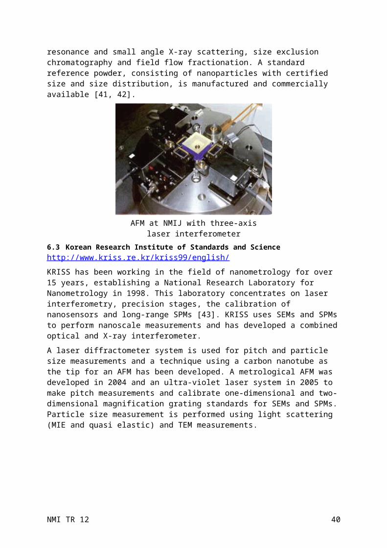
University of Queensland, ARC Centre for Functional Nanomaterialshttp://www.arccfn.org.au
The Centre’s research programs focus on the novel synthesis, characterisation and applications of functional nanomaterials such as nanoparticles, nanotubes, thin films, and nanoporous and nanocomposite materials. They are specifically interested in: clean energy production and utilisation: gas to liquid conversion, hydrogen production
and storage, fuel cells, and high energy density batteries; environmental technologies: photocatalytic reduction of pollutants in water and air,
economic removal and recovery of organic vapours, greenhouse gas reduction and utilisation; and
health care: biomaterials for orthopaedic and cardiovascular applications and tissue repair.
The Centre has its headquarters at the University of Queensland and brings together researchers from the University of New South Wales, Australian National University, University of Western Sydney, four CSIRO divisions, IBM’s Almaden Research Centre and Washington University.
University of Queensland, Australian Institute for Bioengineering and Nanotechnologywww.aibn.uq.edu.au
The Institute will be located in a purpose built world-class research complex. Construction of the $70 million complex began in 2004 and is due for completion in late-2006. It will accommodate around 350 research scientists, engineers and support personnel. Until construction is complete research is continue to work within laboratories throughout the University of Queensland.
Dedicated to bioengineering and nanotechnology, the Institute focuses its research efforts into four major programs: nanotechnology for energy and the environment; cell and tissue engineering; systems biotechnology; and biomolecular nanotechnology.
Specialist facilities include: cell and tissue culture facilities; nanoparticle production and analysis capabilities; polymer synthesis and characterisation; microanalysis; and ultra-high performance flow cytometry.
Queensland University of Technology, Centre for Built Environment and Engineering Researchwww.qut.edu.au
The Centre for Built Environment and Engineering Research is pursuing a number of areas for sustainable and environmentally friendly applications, in the fields of energy generation, energy storage and filtrations systems. These include the creation of titania materials with very large surface areas for photocatalytic applications such as the removal of hydrocarbons from water; in photovoltaic cells for energy production; and to split water molecules for the production of hydrogen and carbon nanotube composite polymer material for photovoltaic cells.
NMI TR 12 43

RMIT University, School of Applied Scienceswww.rmit.edu.au
The work at RMIT includes: process techniques for preparation of metal alloy nanoparticles with a wide range of
magnetic characteristics; development of fabrication techniques for conducting nanoparticle-polymer composite
thin films; wideband and resonantly enhanced lithium niobate optical modulators, polymer
waveguides and electro-optic modulators; grating-assisted couplers; photonic sensors; integration of electro-optic devices with silicon electronics; fabrication of microfluidic channels with integrated heaters, optical waveguides, optic
fibres and sensors with the aim of putting together integrated devices on a single chip; and
fabrication technologies for optical waveguide and microfluidic channel formation, including standard photolithography, spin coating and plasma etching as well as more novel techniques such as soft and hot nanoimprinting/casting, micro-milling and sawing.
University of Sydney, Key Centre for Polymer Colloidswww.kcpc.usyd.edu.au
The Key Centre for Polymer Colloids is an international centre of excellence for research and training, with about 40 Australian and international researchers and research students. It has facilities for the synthesis and characterisation of synthetic and natural polymer colloids. It also provides research support for Australian and international primary and secondary industry. Facilities for particle size analysis include: MATEC applied sciences capillary hydrodynamic fractionator (CHDF-1100); photon correlation spectrometer; Malvern HPPS system; Malvern ZetaSizer; PL-PSDA particle size distribution analyser (HDC); electron microscopy; and acoustosizer.
University of Technology Sydney, Institute for Nanoscale Technologywww.nano.uts.edu.au
Working on: artificial cell membranes that will improve the bio-compatibility of implanted tissue
and cells; targeted drug delivery and gene therapy; super-strength nanograined metals and ceramic materials; nanocoatings and surface texturing for improving prosthetics and implants (including
through sol-gel applications); and light-pipe development for low-power commercial lighting applications.
The Institute is also collaborating with CSIRO to lead the development of the NanoHouse Initiative, designed to demonstrate nanoscience applications in the urban environment, to promote public awareness of nanotechnology and to stimulate public debate and encourage industry uptake of new technologies.
NMI TR 12 44

University of Western Australia, School of Physicswww.uwa.edu.au
Working on: production of chemically stable biocompatible magnetic nanoparticles, involving the
production of polymer based nanoreactors; and magnetic nanosystems (nanoparticles and thin film heterostructures) for potential
applications including microwave shields in computer components to prevent electromagnetic interference, absorbers to control leakage of wireless networks, miniature nanocomposite inductors for mobile phones and additives in adhesives to provide fast setting by selective heating.
University of Western Sydney, Nanomaterials Groupwww.uws.edu.au/about/acadorg/cste/research/links/nodrg
Working on: bio-nanocomposites consisting of nanocrystalline hydroxyapatite, to form biomaterial
coatings on metallic implants; developing nanocomposite coating to replace the copper plating and chrome coating in gravure printing process commonly utilised for large volume, high quality printing;
production of carbon nanotubes and investigating their properties for hydrogen absorption in collaboration with Union Carbide and the Japanese companies NEDO and Itochu;
natural environmental absorbents and looking at methods for in situ production; novel experimental techniques and theoretical models for studying molecular
association, organisation and dynamics; techniques for characterising protein self-association and drug binding; molecular-level understanding of ionic conductance in polymer and gel electrolytes for
the creation of high performance batteries; and nuclear magnetic resonance and modelling techniques for probing porous systems.
University of Wollongong, Centre of Excellence for Electromaterialswww.uow.edu.au/research/rso/grants/outcomes/external/reports/gwallace/wallace.htm
This facility is the base for scientists researching electromaterials and nanotechnology. Recently Professor Gordon Wallace received a A$1.5 million five-year Federation Fellowship to conduct further nanobionics research (the merging of biology and electronics). The university will match the five-year A$1.5 million.
NMI TR 12 45
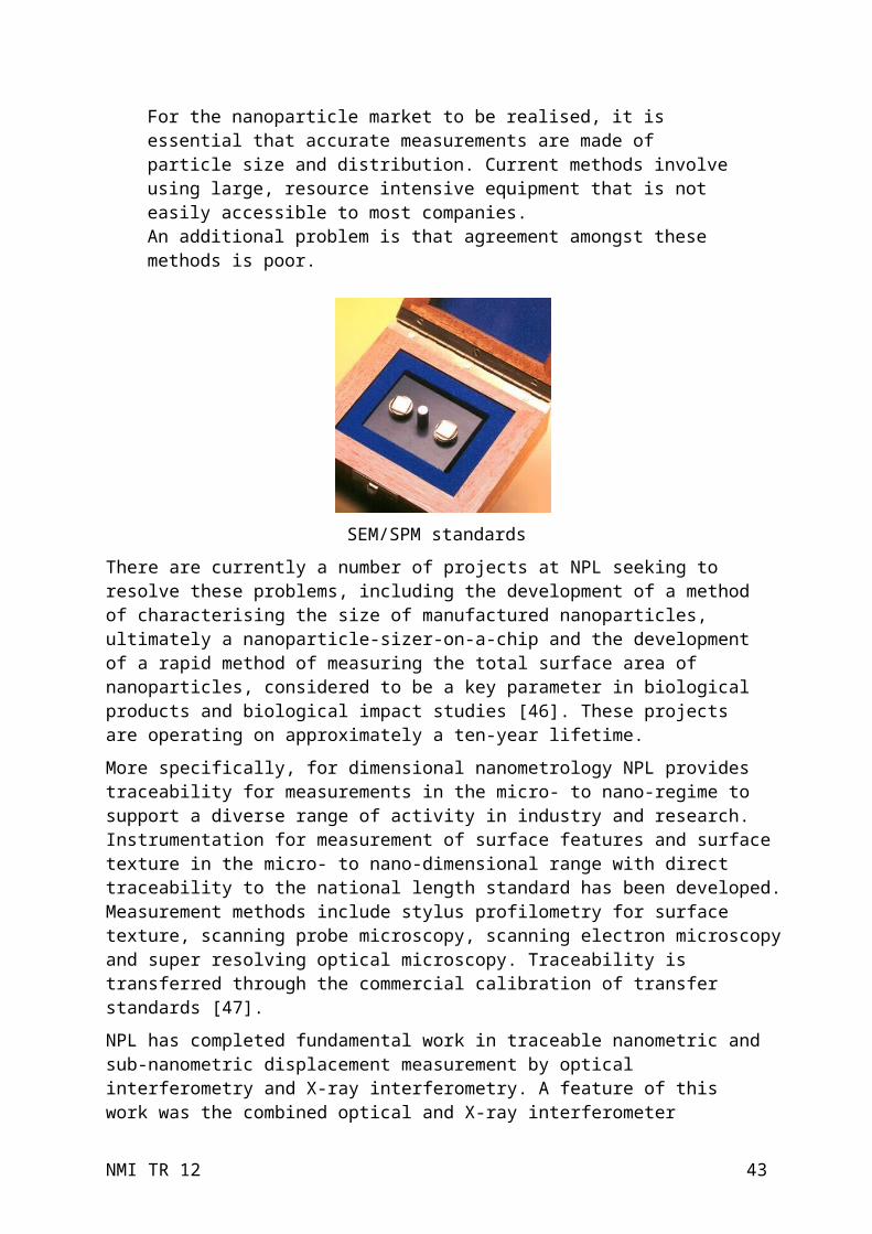
REFERENCES1. MacFarlane, I (2005) Ministerial foreword. In Australian Nanotechnology: Capability
and Commercial Potential, 2nd edition, Invest Australia
2. Nanoscience and Nanotechnologies: Opportunities and Uncertainties (2004) The Royal Society and The Royal Academy of Engineeringhttp://www.nanotec.org.uk/finalReport.htm
3. Small Wonders, Endless Frontiers: A Review of the National Nanotechnology Initiative (2002) National Academy Press, Washington, DChttp://www.nano.gov/html/res/smallwonder.html
4. Nanotechnology Innovation for Tomorrow’s World (2004) European Commission http://ec.europa.eu/research/industrial_technologies/articles/article_2340_en.html
5. Nanotechnology: Shaping The World Atom By Atom (1999) National Science and Technology Council (Committee on Technology) and the Interagency Working Group on Nanoscience, Engineering and Technology, Washington http://www.wtec.org/loyola/nano/IWGN.Public.Brochure/IWGN.Nanotechnology.Brochure.pdf
6. Schattenburg, ML; Smith, HI; Peckerar, MC; Postek, MT (2001) The critical role of metrology in nanotechnology. SPIE Proc. Ser. 4608, 116–124
7. The Need for Measurement and Testing in Nanotechnology (2002) compiled by the High Level Expert Group on Measurement and Testing under the European Framework Programme for Research and Development http://ec.europa.eu/research/fp5/pdf/hleggrowth-nanotechnology.pdf
8. The National Nanotechnology Initiative: Research and Development Leading to a Revolution in Technology and Industry (2006) Subcommittee on Nanoscale Science, Engineering and Technology, Committee on Technology, National Science and Technology Council http://www.nano.gov/NNI_07Budget.pdf
9. Nanotechnology: Enabling Technologies for Australian Innovative Industries (2005) 13th Meeting of the Prime Minister's Science, Engineering and Innovation Council http://www.dest.gov.au/NR/rdonlyres/3CED6715-4ACD-458F-8B8B-9AA040140B9E/4007/NanotechnologyExecutiveSummary.pdf
10. Taniguchi, N (1974) On the basic concept of nanotechnology. Proc. Int. Conf. Prod. Eng. Tokyo, Part II, p18, Japan Society of Precision Engineering
11. Binks, P. (2005) The nanotechnology market: Challenges and opportunities. Workshop on Nanotechnology: The Building Block for Tomorrow’s Advanced Technology, University of Western Australia
12. Nanotechnology: Where Does the US Stand? (2005) Hearing Charter before the Research Subcommittee of the Committee on Science of the House of Representatives http://www.house.gov/science/hearings/research05/june29/charter.pdf
13. Eom, C. (2005) Nanotechnology in Korea. Technical Committee for Length, Asia Pacific Metrology Programme
14. European Support for Nanotechnology Small and Medium-sized Enterprises (2005) Nanoforum http://www.nanoforum.org/
NMI TR 12 46

15. Towards a European Strategy for Nanotechnology (2004) European Commission, Brussels ftp://ftp.cordis.europa.eu/pub/nanotechnology/docs/nano_com_en.pdf
16. Nanosciences and Nanotechnologies: An Action Plan for Europe 2005-2009 (2005) European Commission, Brussels http://ec.europa.eu/research/industrial_technologies/pdf/nano_action_plan_en.pdf
17. Forecasting Productivity Growth: 2004 to 2024 (2006) Department of Communications, Information Technology and the Arts http://www.dcita.gov.au/__data/assets/pdf_file/37831/Forecasting_Productivity_Growth_2004_to_2024.PDF
18. Small Scale Technologies: Directions for Victoria (2003) Centre for Strategic Economic Studies, Victoria University, Melbourne http://www.cfses.com/documents/CSES_Nano_Report_Dec_03.PDF
19. Nanotechnology and Australian Business: Results of an Industry Survey conducted by Nanotechnology Victoria (2005) Second Australian Nanotechnology Conference, Melbourne http://www.nanovic.com.au/downloads/conferencebrochure.pdf
20. PAS 71:2005 Vocabulary — Nanoparticleshttp://www.bsi-global.com/Manufacturing/Nano/index.xalter
21. Australian Directory of Nanotechnology Service Providers (2004) The Warren Centre for Advanced Engineering, University of Sydney
22. Australian Nanotechnology Company Directory (2005) Invest Australia
23. Australian Nanotechnology Research Institution Directory (2005) Invest Australia
24. Sheremeta, L (2005) The Ethical, Economic, Environmental, Legal and Social Issues (NE3LS) of Nanotechnology: A View From Canada. Health Law Institute, Faculty of Law, University of Alberta
25. Nanoparticles: An Occupational Hygiene Review (2004) Institute of Occupational Medicine, Edinburgh
26. Nanomaterials: A Risk to Health at Work? (2004) First International Symposium on Occupational Health Implications of Nanomaterials, Derbyshire, UK http://www.hsl.gov.uk/capabilities/nanosymrep_final.pdf
27. Characterising the Potential Risks Posed by Engineered Nanoparticles (2005) Department for Environment, Food and Rural Affairs, London http://nanoparticles.org/pdf/nanoparticles-riskreport.pdf
28. Nordan, MM and Holman, MW (2005) A prudent approach to nanotechnology environmental, health, and safety risks. Ind. Biotechnol. 1(3), 146–149
29. Scientific Committee on Emerging and Newly Identified Health Risks Opinion on the Appropriateness of Existing Methodologies to Assess the Potential Risks Associated with Engineered and Adventitious Products of Nanotechnologies (2005) European Commission, Health and Consumer Protection Directorate-General http://ec.europa.eu/health/ph_risk/committees/04_scenihr/docs/scenihr_o_003.pdf
30. Maynard, A. and Kuempel, E. (2005) Airborne nanostructured particles and occupational health. J. Nanopart. Res. 7, 587–614
31. International Vocabulary of Basic and General Terms in Metrology (1993) International Bureau of Weights and Measures
NMI TR 12 47

32. Korpelainen, V and Lassila, A (2006) Calibration of a commercial AFM: Interferometric traceability for a coordinate system. NanoScale 2006, Switzerland
33. First International Symposium on Standard Materials and Metrology for Nanotechnology (2004) National Institute of Advanced Industrial Science and Technology, Tokyo
34. Wilkening, G and Koenders, L eds (2005) Nanoscale Calibration Standards and Methods: Dimensional and Related Measurements in the Micro- and Nanometre Range. Wiley-VCH, Weinheim, Germany
35. Wilkening, G (2005) Report to the 10th Working Group on Dimensional Metrology, Consultative Committee for Length, International Bureau of Weights and Measures
36. Koenders, L (2003) WGDM7: Preliminary Comparison on Nanometrology According to the Rules of CCL Key Comparisons. Nano 2: Step Height Standards — Final Report http://www.bipm.org/utils/common/pdf/final_reports/L/S2/CCL-S2.pdf
37. Kopanski, J (2005) Report: Nanotechnology Research and Development at the National Institute of Standards and Technology
38. Postek, MT (2004) Nanometrology: fundamental for realizing products at the nanoscale. Micro Nano Breakthrough Conference 2004, Washington
39. Postek, MT (2005) Nanometer-scale Metrology. National Institute of Science and Technologyhttp://www.mel.nist.gov/div821/webdocs-14/nanoscale-metrology_2001.pdf
40. Takatsuji, T (2005) National project: Research and development of 3D nanoscale certified reference materials. 21st APMP General Assembly, TCL Report
41. Nanoscale Characterisation of Advanced Materials (2005) APEC Workshop, Industrial Technology Research Institute, Taiwan
42. Report on Nanoparticle Metrology (2005) National Metrology Institute of Japan
43. Eom, TB (2005) Nanometrology in KRISS. 21st APMP General Assembly, TCL Report
44. Wilkening, G. (2005) Presentation on Dimensional Nanometrology at PTB: Recent Developments, Physikalisch-Technische Bundesanstalt
45. Brand, U and Kirchhoff, J (2005) A micro-CMM with metrology frame for low uncertainty measurements. Meas. Sci. Technol. 16(12), 2489–2497
46. Cumpson, P (2006) Roadmap for NPL manufacturing theme: Micro and Nanoparticles: rapid, reliable multi-property analysis techniques National Physical Laboratory
47. Leach, R; Chetwynd D; Blunt, L; Haycocks, J; Harris, P; Jackson, K; Oldfield, S and Reilly, S (2006) Recent advances in traceable nanoscale dimension and force metrology in the UK. Meas. Sci. Technol. 17(3), 467–476
48. Lewis, A (2002) The NPL Small CMM. Euromet Length Workshop
49. The Measurement of Engineered Nanoparticles (2005) Presentation to the Micro and Nano Technology Measurement Club, London
50. Lan, YP (2005) Dimensional nanometrology developments at CMS. 21st APMP General Assembly, TCL Report
NMI TR 12 48

51. Pekelsky, JR; Nistico, BJ; Eves, BJ and Decker, JE (2006) Imaging laser-diffractometer for traceable grating pitch calibration (poster). NanoScale 2006, Switzerland
52. Project Proposal on Technological Cooperative Framework on Nanoscale Analytical and Measurement Methods (2006) APEC
53. Preliminary Interlaboratory Comparison on Nanoparticle Size Characterization Comparison Report First Draft (2005) APEC
54. Koenders, L (2003) WGDM7: Preliminary Comparison on Nanometrology According to the Rules of CCL Key Comparisons. Nano 3: Line Scale Standards — Final Report
55. Meli, F (2000) WGDM-7: WGDM7: Preliminary Comparison on Nanometrology According to the Rules of CCL Key Comparisons. Nano 4: 1D Gratings — Final Report, Draft B
NMI TR 12 49