Embed Size (px)
Citation preview

REVIEWS OF MODERN PHYSICS, VOLUME 73, JULY 2001
Nobel Lecture: The double heterostructure concept and its applicationsin physics, electronics, and technology*
Zhores I. Alferov
A. F. Ioffe Physico-Technical Institute, Russian Academy of Sciences,St. Petersburg 194021, Russian Federation
(Published 22 October 2001)
I. INTRODUCTION
It is impossible to imagine now modern solid-statephysics without semiconductor heterostructures. Semi-conductor heterostructures and, particularly, double het-erostructures, including quantum wells, wires, and dots,are today the subject of research of two-thirds of thesemiconductor physics community.
The ability to control the type of conductivity of asemiconductor material by doping with various impuri-ties and the idea of injecting nonequilibrium charge car-riers could be said to be the seeds from which semicon-ductor electronics developed. Heterostructuresdeveloped from these beginnings, making it possible tosolve the considerably more general problem of control-ling the fundamental parameters inside the semiconduc-tor crystals and devices: band gaps, effective masses ofthe charge carriers and the mobilities, refractive indices,electron energy spectrum, etc.
Development of the physics and technology of semi-conductor heterostructures has resulted in remarkablechanges in our everyday life. Heterostructure electronicsare widely used in many areas of human civilization. It ishardly possible to imagine our recent life without doubleheterostructure (DHS) laser-based telecommunicationsystems, heterostructure-based light-emitting diodes(LED’s), heterostructure bipolar transistors, or low-noise high-electron-mobility transistors for high-frequency applications including, for example, satellitetelevision. Double-heterostructure lasers now enterpractically every house with CD players. Heterostruc-ture solar cells have been widely used for space and ter-restrial applications.
Our interest in semiconductor heterostructures wasnot occasional. Systematic studies of semiconductorswere started in the early 1930s at the Physico-TechnicalInstitute under the direct leadership of its founder,Abraham Ioffe. V. P. Zhuze and B. V. Kurchatov studiedthe intrinsic and impurity conductivity of semiconduc-tors in 1932, and the same year Ioffe and Ya. I. Frenkelcreated a theory of rectification in a metal-semiconductor contact based on the tunneling phenom-
*The 2000 Nobel Prize in Physics was shared by Zhores I.Alferov, Jack Kilby, and Herbert Kroemer. This lecture is thetext of Professor Alferov’s address on the occasion of theaward.
0034-6861/2001/73(3)/767(16)/$23.20 767
enon (Frenkel and Ioffe, 1932; Zhuze and Kurchatov,1932a, 1932b). In 1931 and 1936 Frenkel published hisfamous articles where he predicted, gave the name, anddeveloped the theory of excitons in semiconductors, andE. F. Gross experimentally discovered excitons in 1951(Frenkel, 1931, 1936; Gross and Karryev, 1952a, 1952b).The first diffusion theory of p-n heterojunction rectifi-cation, which became the base for W. Shockley’s p-njunction theory, was published by B. I. Davydov in 1939(Davydov, 1939). Because of Ioffe’s initiative in the late1940s at the Physico-Technical Institute, research intointermetallic compounds was begun. Theoretical predic-tion of semiconductor properties in A3B5 compoundsand their subsequent experimental discovery were doneindependently by H. Welker and (on the example ofInSb) N. A. Gorunova and A. R. Regel at the Physico-Technical Institute (Goryunova, 1951; Blum et al., 1952;Welker, 1953). We benefited a lot from the high degreeof theoretical, technological, and experimental expertisein this area at the Ioffe Institute at that time.
II. CLASSICAL HETEROSTRUCTURE
The idea of using heterojunctions in semiconductorelectronics was put forward at the very dawn of the elec-tronic era. In the first patent concerned with p-n junc-tion transistors, Shockley (1951) proposed a wide-gapemitter to obtain unidirectional injection. A. I. Gubanovat our Institute first theoretically analyzed current-voltage characteristics of isotype and anisotype hetero-junctions (Gubanov, 1950, 1951) but the importanttheoretical considerations at this early stage of hetero-structure research were put forward by H. Kroemer,who introduced the concept of quasielectric and quasi-magnetic fields in a graded heterojunction and made anassumption that heterojunctions might exhibit extremelyhigh injection efficiencies in comparison to homojunc-tions (Kroemer, 1957a, 1957b). In the same period therewere various suggestions about applying heterostruc-tures in semiconductor solar cells.
The proposal of p-n junction semiconductor lasers(Basov et al., 1961), the experimental observation of ef-fective radiative recombination in GaAs p-n structurewith a possible stimulated emission (Nasledov et al.,1962), and the creation of p-n junction lasers and LED’s(Hall et al., 1962; Holonyak and Bevacgua, 1962; Nathanet al., 1962) were the seeds from which semiconductoroptoelectronics started to grow. However, lasers were
© The Nobel Foundation 2000

768 Zhores I. Alferov: The double heterostructure concept
not efficient because of high optical and electrical losses.The threshold currents were very high, and low tem-perature was necessary for lasing. The efficiency ofLED’s was very low, as well, due to high internal losses.
The important step was made immediatly after thecreation of p-n junction lasers when the concept of thedouble heterostructure laser was formulated indepen-dently by us and Kroemer (Alferov and Kazarinov, 1963;Kroemer, 1963). In his article Kroemer proposed to usethe double heterostructures for carrier confinement inthe active region. He proposed that ‘‘laser action shouldbe obtainable in many of the indirect gap semiconduc-tors and improved in the direct gap ones, if [it] is pos-sible to supply them with a pair of heterojunctioninjectors.’’
In our patent we also outlined the possibility ofachieving a high density of injected carriers and inversepopulation by ‘‘double’’ injection. We especially pointedout that homojunction lasers ‘‘do not provide cw at el-evated temperatures,’’ and an additional advantage ofDH lasers that we considered was the possibility ‘‘to en-large the emitting surface and to use new materials invarious regions of the spectrum.’’
Initially the theoretical progress was much faster thanexperimental realization. In 1966 (Alferov et al., 1966),we predicted that the density of injected carriers couldexceed the carrier density in a wide-gap emitter by sev-eral orders of magnitude (the ‘‘superjunction’’ effect).The same year, in a paper submitted to a new Sovietjournal, Fizika i Tekhnika Poluprovodnikov (SovietPhysics Semiconductors), I summarized our understand-ing of the main advantages of the double heterostruc-ture for different devices, especially for lasers and high-power rectifiers:
‘‘The recombination, light-emitting, and populationinversion zones coincide and are concentrated in themiddle layer. Due to potential barriers at the bound-aries of semiconductors having forbidden bands of dif-ferent width, the through currents of electrons andholes are completely absent, even under strong for-ward voltages, and there is no recombination in theemitters (in contrast to p-i-n , p-n-n1, n-p-p1 ho-mostructures, in which the recombination plays thedominant role) . . . . Because of a considerable differ-ence between the permittivities, the light is com-pletely concentrated in the middle layer, which acts asa high-grade waveguide, and thus there are no lightlosses in the passive regions (emitters)’’ (Alferov,1966).
Here are the most important peculiarities of semicon-ductor heterostructures we emphasized at that time: (i)superinjection of carriers, (ii) optical confinement, and(iii) electron confinement.
The realization of the wide-gap window effect wasvery important for photodetectors, solar cells, and LEDapplications. It permitted us to broaden considerablyand to control precisely the spectral region for solar cellsand photodetectors and to improve drastically the effi-ciency of LED’s. The main physical phenomena in
Rev. Mod. Phys., Vol. 73, No. 3, July 2001
double and single classical heterostructures are shown inFig. 1. Then it was only necessary to find heterostruc-tures in which these phenomena could be realized.
At that time general skepticism existed with respect tothe possibility of creating the ‘‘ideal’’ heterojunctionwith a defect-free interface and first of all with theoret-ical injection properties. Even a very pioneering study ofthe first lattice-matched epitaxially grown single-crystalheterojunctions Ge-GaAs by R. L. Anderson (1960,1962) did not give any proof of the injection of nonequi-librium carriers in heterostructures. Actual realization ofan efficient wide-gap emitter was considered to be nextto impossible, and the patent for the double-heterostructure laser was often referred to as a ‘‘paperpatent.’’
Mostly due to this general skepticism there existedonly a few groups trying to find the ‘‘ideal couple,’’which was, naturally, a difficult problem. Many condi-tions of compatibility needed to be met between ther-mal, electrical, and crystallochemical properties and be-tween the crystal and the band structure of thecontacting materials.
A lucky combination of a number of properties, i.e., asmall effective mass and wide energy gap, effective ra-diative recombination, and a sharp optical absorptionedge due to the ‘‘direct’’ band structure, a high mobilityat the absolute minimum of the conduction band, and itsstrong reduction of the nearest minimum at the (100)point ensured for GaAs even at that time a place ofhonor in semiconductor physics and electronics. Sincethe maximum effect is obtained by using heterojunctionsbetween the semiconductor serving as the active regionand a more wideband material, the most promising sys-tems looked at in that time were GaP-GaAs and AlAs-GaAs. To be compatible, materials of the ‘‘couple’’should have, as the first and the most important condi-
FIG. 1. Main physical phenomena in classical heterostructures:(a) One-side injection and superinjection; (b) diffusion inbuilt-in quasielectric field; (c) electron and optical confine-ment; (d) wide-gap window effect; (e) diagonal tunnelingthrough a heterostructure interface.
769Zhores I. Alferov: The double heterostructure concept
tion, close values of the lattice constants; therefore het-erojunctions in the system AlAs-GaAs were preferable.However, prior to starting work on the preparation andstudy of these heterojunctions one had to overcome acertain psychological barrier. AlAs had been synthesizedlong ago (Natta and Passerini, 1928; Goldschmidt, 1929),but many properties of this compound remained unstud-ied, since AlAs was known to be chemically unstableand to decompose in moist air. The possibility of prepar-ing stable and adequate applications of heterojunctionsin this system seemed to be not very promising.
Initially, our attempts to create double heterostruc-tures were related to a lattice-mismatched GaAsP sys-tem. And we succeeded in fabricating by vapor-phaseepitaxy the first DHS lasers in this system. However, dueto lattice mismatch, the lasing, like that in homojunctionlasers, occurred only at liquid-nitrogen temperatures(Alferov, Garbuzov, et al., 1967). I would like to mentionthat, curiously, it was the first practical result obtainedfor a lattice-mismatched, even partially relaxed, system.
Our experience, which we got from studying theGaAsP system, was very important for understandingmany specific heterojunction physical properties and thebasics of heteroepitaxy. The development of the multi-chamber vapor-phase epitaxy method for the GaAsPsystem permitted us to create in 1970 superlattice struc-tures with a 200-Å period and to demonstrate the split-ting of the conduction band (Alferov, Zhilyaev, andShmartsev, 1971).
But from the general point of view at the end of 1966we came to a conclusion that even a small lattice mis-match in heterostructures GaP0.15As0.85-GaAs did notpermit us to realize potential advantages of the doubleheterostructure. At that time my co-worker D. N.Tret’yakov told me that some small crystals ofAlxGa12xAs solid solutions of different compositions,which had been prepared two years ago by cooling froma melt, were put in a desk drawer by Dr. A. S. Bort-shevsky and nothing happened to them. It immediatelybecame clear that AlxGa12xAs solid solutions turnedout to be chemically stable and suitable for the prepara-tion of durable heterostructures and devices. Studies ofphase diagrams and the growth kinetics in this systemand development of the liquid-phase epitaxy method,especially for heterostructure growth, soon resulted infabrication of the first lattice-matched AlGaAs hetero-structures. When we published the first paper on thissubject, we felt lucky to be the first to find a unique,practically ideal lattice-matched system for GaAs, but asfrequently happened, simultaneously and independentlythe same results were achieved by H. Rupprecht and J.Woodall at the T. Watson IBM Research Center (Alf-erov, Andreev, et al., 1967; Rupprecht et al., 1967).
From then on, progress in the semiconductor hetero-structure area was very rapid. First of all, we experimen-tally proved the unique injection properties of the wide-gap emitters and superinjection effect (Alferov,Andreev, et al., 1968a) and the stimulated emission inAlGaAs double heterostructures (Alferov, Andreev,et al., 1968b), established the band diagram of the
Rev. Mod. Phys., Vol. 73, No. 3, July 2001
AlxGa12xAs-GaAsx heterojunction, and carefully stud-ied luminescence properties, diffusion of carriers in agraded heterostructure, and very interesting peculiari-ties of the current flow through the heterojunction. Thecurrent flow is similar, for instance, to diagonaltunneling-recombination transitions directly betweenholes of the narrow-band and electrons of the wide-bandheterojunction components (Alferov, Andreev,Korol’kov, Portnoi, and Tret’yakov, 1969; Alferov, An-dreev, Korol’kov, Portnoi, and Yakovenko, 1969a; Alf-erov, Garbuzov, et al., 1969; Alferov, 1970).
At the same time, we created some important devicesthat realized the main advantages of the heterostructureconcepts:
—DHS lasers with low threshold at room tempera-ture. (Fig. 2) (Alferov, Andreev, Portnoy, and Trukan,1969)
—Highly effective LED’s using semiconductor hetero-structures and double heterostructures (Alferov, An-dreev, Korol’kov, Portnoi, and Yakovenko, 1969b)
—Heterostructure solar cells (Alferov, Andreev, Ka-gan, et al., 1970)
—Heterostructure bipolar transistor (Alferov, Ahme-dov, et al., 1973)
—Heterostructure p-n-p-n switching devices (Alf-erov, Andreev, Korol’kov, Nikitin, and Yakovenko,1970).
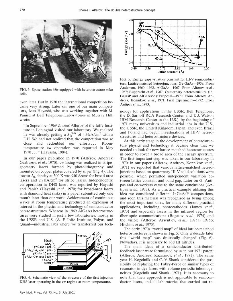
One of the first successful applications in industrial-scale production in our country was heterostructure so-lar cells in space research. We transferred our technol-ogy to the Quant company and, since 1974, GaAlAssolar cells have been installed on many of our sputniks.Our space station Mir (Fig. 3) used them for 15 years.
Most of these results were achieved afterwards inother laboratories in one to two years and in some cases
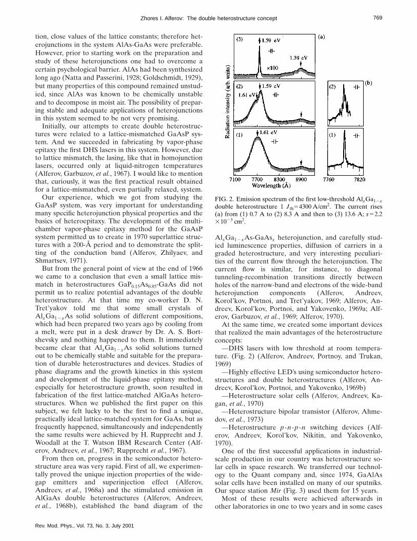
FIG. 2. Emission spectrum of the first low-threshold AlxGa12x
double heterostructure 1 J th54300 A/cm2. The current rises(a) from (1) 0.7 A to (2) 8.3 A and then to (3) 13.6 A; s52.231023 cm2.
770 Zhores I. Alferov: The double heterostructure concept
even later. But in 1970 the international competition be-came very strong. Later on, one of our main competi-tors, Izuo Hayashi, who was working together with M.Panish at Bell Telephone Laboratories in Murray Hill,wrote:
‘‘In September 1969 Zhores Alferov of the Ioffe Insti-tute in Leningrad visited our laboratory. We realizedhe was already getting a J th
(300) of 4.3 kA/cm2 with aDH. We had not realized that the competition was soclose and redoubled our efforts . . . Room-temperature cw operation was reported in May1970 . . . ’’ (Hayashi, 1984).
In our paper published in 1970 (Alferov, Andreev,Garbuzov, et al., 1970), cw lasing was realized in stripe-geometry lasers formed by photolithography andmounted on copper plates covered by silver (Fig. 4). Thelowest J th density at 300 K was 940 A/cm2 for broad-arealasers and 2.7 kA/cm2 for stripe lasers. Independently,cw operation in DHS lasers was reported by Hayashiand Panish (Hayashi et al., 1970; for broad-area laserswith diamond heat sinks) in a paper submitted only onemonth later than our work. Achievement of continuouswaves at room temperature produced an explosion ofinterest in the physics and technology of semiconductorheterostructures. Whereas in 1969 AlGaAs heterostruc-tures were studied in just a few laboratories, mostly inthe USSR and U.S. (A. F. Ioffe Institute, Polyus, andQuant—industrial labs where we transferred our tech-
FIG. 3. Space station Mir equipped with heterostructure solarcells.
FIG. 4. Schematic view of the structure of the first injectionDHS laser operating in the cw regime at room temperature.
Rev. Mod. Phys., Vol. 73, No. 3, July 2001
nology for applications in the USSR; Bell Telephone,the D. Sarnoff RCA Research Center, and T. J. WatsonIBM Research Center in the U.S.), by the beginning of1971 many universities and industrial labs in the U.S.,the USSR, the United Kingdom, Japan, and even Braziland Poland had begun investigations of III-V hetero-structures and heterostructure devices.
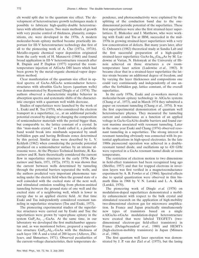
At this early stage in the development of heterostruc-ture physics and technology it became clear that weneeded to look for new lattice-matched heterostructuresin order to cover a broad area of the energy spectrum.The first important step was taken in our laboratory in1970: in our paper (Alferov, Andreev, Konnikov, et al.,1971) we reported that various lattice-matched hetero-junctions based on quaternary III-V solid solutions werepossible, which permitted independent variation be-tween lattice constant and band gap. Later on G. Anti-pas and co-workers came to the same conclusions (An-tipas et al., 1973). As a practical example utilizing thisidea we considered different InGaAsP compositions,and soon this material was recognized as being amongthe most important ones, for many different practicalapplications, including photocathodes (James et al.,1973) and especially lasers in the infrared region forfiber-optic communications (Bogatov et al., 1974) andthe visible (Alferov, Arsent’ev, et al., 1975a, 1975b;Hitchins et al., 1975).
The early 1970s ‘‘world map’’ of ideal lattice-matchedheterostructures is shown in Fig. 5. Only a decade laterthis ‘‘world map’’ was drastically changed (Fig. 6).Nowadays, it is necessary to add III nitrides.
The main ideas of a semiconductor distributed-feedback laser were formulated by us in our 1971 patent(Alferov, Andreev, Kazarinov, et al., 1971). The sameyear H. Kogelnilk and C. V. Shank considered the pos-sibility of replacing the Fabry-Perot or similar types ofresonator in dye lasers with volume periodic inhomoge-neities (Kogelnik and Shank, 1971). It is necessary tonote that their approach is not applicable to semicon-ductor lasers, and all laboratories that carried out re-
FIG. 5. Energy gaps vs lattice constant for III-V semiconduc-tors. Lattice-matched heterojunctions: Ge-GaAs—1959. FromAnderson, 1960, 1962. AlGaAs—1967. From Alferov et al.,1967; Rupprecht et al., 1967. Quaternary heterostructure (In-GaAsP and AlGaAsSb): Proposal—1970. From Alferov, An-dreev, Konnikov, et al., 1971; First experiment—1972. FromAntipas et al., 1973.

771Zhores I. Alferov: The double heterostructure concept
search in distributed-feedback and distributed-Bragg-reflector semiconductor lasers used the ideas formulatedin Alferov, Andreev, Kazarinov, et al. (1971):
(1) Diffraction grating created not in volume, but on asurface waveguide layer.
(2) Interaction of waveguide modes with a surface dif-fraction grating, which gives not only distributed feed-back but also highly collimated light output.
A detailed theoretical analysis of the semiconductorlaser with surface diffraction grating was published in1972 (Kazarinov and Suris, 1972b). In this paper the au-thors established the way to obtain single-frequencygeneration. The first semiconductor lasers using surfacediffraction gratings and distributed feedback were real-ized practically simultaneously at the Physico-TechnicalInstitute (Alferov et al., 1974, 1975), Caltech (Nakamuraet al., 1973), and Xerox Laboratory in Palo Alto (Scifreset al., 1974).
In the early 1980s Kroemer and G. Griffiths (1983)published a paper that stimulated strong interest instaggered-lineup heterostructures (type-II heterojunc-tion). Spatial separation of electrons and holes at theinterface results in tunability of their optical properties(Alferov, Garbuzov, et al., 1969; Baranov et al., 1986).Staggered band alignment makes it possible to realizeoptical emission with a photon energy much smallerthan the band-gap energy of each of the semiconductorsforming a heterojunction. The demonstration of an in-jection laser based on a type-II GaInAsSb-GaSb hetero-junction (Baranov et al., 1986) showed promise for thecreation of effective coherent light sources in the infra-red optical range. Radiation in such a device is due tothe recombination of electrons and holes localized inself-consistent potential wells at different sides of theheterointerface. Thus type-II heterostructures open pos-sibilities both for fundamental physics and for deviceapplications, which cannot be realized with type-I het-erostructures in the III-V material systems. However,
FIG. 6. Energy gaps vs lattice constants for semiconductors ofIV elements, III-V and II(IV)-VI compounds, and magneticmaterials in parentheses. Lines connecting the semiconductors,solid for the III-V’s and dashed for the others, indicate quan-tum heterostructures that have been investigated.
Rev. Mod. Phys., Vol. 73, No. 3, July 2001
practical applications of these structures are still ham-pered by a poor understanding of their fundamentalproperties and scarcity of actual systems, which havebeen studied experimentally up to now.
To summarize this brief review of classical hetero-structure development, we can classify the most impor-tant as follows:
CLASSICAL HETEROSTRUCTURES
I. Fundamental physical phenomena (Fig. 1)
• One-side injection• Superinjection• Diffusion in built-in quasielectric fields• Electron confinement• Optical confinement• Wide-gap window effect• Diagonal tunneling through heterostructure inter-
face
II. Important applications in electronics
• Semiconductor lasers—Low threshold and continuouswaves at room temperature, distributed-feedback anddistributed-Bragg-reflector lasers, vertical surface emit-ting lasers, IR type-II heterostructure lasers
• High-efficiently LED’s• Solar cells and photodetectors, based on wide-gap
window effect• Semiconductor integrated optics, based on semicon-
ductor distributed-feedback and distributed-Bragg-reflector lasers
• Bipolar wide-gap transistors• Transistors, thyristors, and dynistors with photonic
signal transmission• High-power diodes and thyristors• Infrared to visible converters• Efficient cold cathodes
III. Important technological peculiarities
• Lattice-matched structures are necessary in prin-ciple
• Multicomponent solid solutions are used for latticematching
• Epitaxial growth technology is needed in principle
Concluding this concise summary of the early devel-opment of bulk heterostructures, one may say that theinvention of an ‘‘ideal’’ heterojunction and the introduc-tion of the heterostructure concept into semiconductorphysics and technology have led to the discovery of newphysical effects, pivotal improvement in the characteris-tics of practically all known semiconductor devices, andthe invention of new ones.
III. HETEROSTRUCTURE QUANTUM WELLS ANDSUPERLATTICES
Owing to electron confinement, the double-heterostructure laser became an important precursor ofthe quantum well structure: when a middle layer had athickness of some hundred angstroms, the electron lev-
772 Zhores I. Alferov: The double heterostructure concept
els would split due to the quantum size effect. The de-velopment of heterostructure growth techniques made itpossibile to fabricate high-quality-double heterostruc-tures with ultrathin layers. Two main methods of growthwith very precise control of thickness, planarity, compo-sitions, etc. were developed in the 1970s. A modernmolecular-beam epitaxy method became practically im-portant for III-V heterostructure technology due first ofall to the pioneering work of A. Cho (1971a, 1971b).Metallo-organic chemical vapor deposition originatedfrom the early work of H. Manasevit (1968) and foundbroad application in III-V heterostructure research afterR. Dupuis and P. Dapkus (1977) reported the room-temperature injection of AlGaAs DH lasers which hadbeen grown by the metal-organic chemical-vapor depo-sition method.
Clear manifestation of the quantum size effect in op-tical spectra of GaAs-AlGaAs semiconductor hetero-structures with ultrathin GaAs layers (quantum wells)was demonstrated by Raymond Dingle et al. (1974). Theauthors observed a characteristic steplike behavior inabsorption spectra and systematic shifts of the character-istic energies with a quantum well width decrease.
Studies of superlattices were launched by the work ofL. Esaki and R. Tsu (1970), who considered the electrontransport in a superlattice, i.e., at an additional periodicpotential created by doping or changing the compositionof semiconductor materials with the period bigger than,but comparable to, the lattice constant of a crystal. Inthis ‘‘man-made crystal,’’ as Esaki called it, a parabolicband would break into minibands separated by smallforbidden gaps and having Brillouin zones determinedby this period. Similar ideas were described by L. V.Keldysh (1962) when considering the periodic potentialproduced on a semiconductor surface by an intense ul-trasonic wave. At the Physico-Technical Institute, R. Ka-zarinov and R. Suris theoretically considered the currentflow in superlattice structures in the early 1970s (Ka-zarinov and Suris, 1971, 1972a, 1973). It was shown thatthe current between wells determined by tunnelingthrough the potential barriers separated the wells, andthe authors predicted very important phenomena: tun-neling under the electric field when the ground state of awell coincided with the excited state of the next well,and stimulated emission resulting from photon-assistedtunneling between the ground state of one well and theexcited state of a neighboring well, which is lower inenergy due to an applied electric field. At that timeEsaki and Tsu independently considered resonant tun-neling in superlattice structures (Tsu and Esaki, 1973).
The pioneering experimental studies of the superlat-tice structures were carried out by Esaki and Tsu: thesuperlattices were grown by vapor-phase epitaxy in thesystem GaPxAs12x-GaAs. At the same time, in ourlaboratory we developed the first multichamber appara-tus and, as was mentioned before, prepared a superlat-tice structure GaP0.3Al0.7-GaAs with the thickness ofeach layer 100 Å and a total of 200 layers (Alferov, Zhi-lyaev, and Shmartsev, 1971). Observed peculiarities ofthe current-voltage characteristics, their temperature de-
Rev. Mod. Phys., Vol. 73, No. 3, July 2001
pendence, and photoconductivity were explained by thesplitting of the conduction band due to the one-dimensional periodic potential of the superlattice. Thesefirst superlattices were also the first strained-layer super-lattices. E. Blakeslee and J. Matthews, who were work-ing with Esaki and Tsu at IBM, succeeded in the mid-1970s in growing strained-layer superlattices with a verylow concentration of defects. But many years later, afterG. Osbourn’s (1982) theoretical study at Sandia Lab andthe first successful preparation of a high-qualitystrained-layer superlattice GaAs-In0.2Ga0.8As by M. Lu-dowise at Varian, N. Holonyak at the University of Illi-nois achieved on those structures a cw room-temperature laser action (Ludowise et al., 1983). Itbecame clear that in a strained-layer superlattice the lat-tice strain became an additional degree of freedom, andby varying the layer thicknesses and compositions onecould vary continuously and independently of one an-other the forbidden gap, lattice constant, of the overallsuperlattice.
In the early 1970s, Esaki and co-workers moved tomolecular-beam epitaxy technology in AlGaAs systems(Chang et al., 1973), and in March 1974 they submitted apaper on resonant tunneling (Chang et al., 1974). It wasthe first experimental demonstration of quantum wellheterostructure physics. They measured the tunnelingcurrent and conductance as a function of an appliedvoltage in GaAs-GaAlAs double barriers and found cur-rent maxima associated with resonant tunneling. Laterin the same year Esaki and Chang (1974) observed reso-nant tunneling in a superlattice. The strong interest inresonant tunneling obviously was connected with its po-tential applications in high-speed electronics. In the late1980s picosecond operation was achieved in a double-resonant tunnel diode, and oscillations up to 420 GHzwere reported in a GaAs resonant tunnel diode at roomtemperature.
The restriction of electron motion to two dimensionsin field-effect transistors had been recognized long ago(Shriffer, 1957) and that for trapped electrons in inver-sion layers was first verified in a magnetoconductanceexperiment by A. B. Fowler et al. (1966). Spectral effectsdue to spatial quantization were observed in thin bis-muth films in 1968 by V. N. Lutskii and L. A. Kulik(Lutskii, 1970).
The pioneering work of Dingle et al. (1978) onmodulation-doped superlattices demonstrated a mobil-ity enhancement with respect to the bulk crystal andstimulated research on the application of high-mobilitytwo-dimensional electron gas for microwave amplifica-tion. In France and Japan practically simultaneouslynew types of transistors based on a singlenAlGaAs-nGaAs modulation-doped heterostructurewere created that were labeled TEGFET’s (two-dimensional electron-gas field-effect transistors) inFrance (Delagebeaudeuf et al., 1980) and HEMT’s(high-electron-mobility transistors) in Japan (Mimuraet al., 1980).
The first quantum well laser operation was demon-strated by J. P. van der Ziel et al. (1975), but the lasing

773Zhores I. Alferov: The double heterostructure concept
parameters were much worse than for average DHS la-sers. In 1978 Dupuis and Dapkus, in collaboration withHolonyak, first reported on a quantum well laser withparameters comparable to those of conventional DHSlasers (Dupuis et al., 1978). The name ‘‘quantum well’’was used in that paper. The real advantages of quantumwell lasers were demonstrated much later by W. T. Tsangat Bell Telephone Laboratories. Thanks to many im-provements in molecular-beam epitaxy growth technol-ogy and the introduction of an optimized structure(GRIN SCH), he found threshold currents as low as160 A/cm2 (Tsang, 1982).
We started to develop molecular-beam epitaxy andmetal-organic chemical vapor deposition methods forgrowing III-V heterostructures only in the late 1970s.First of all, we stimulated the design and construction ofthe first Soviet molecular-beam epitaxy machine in ourelectronic industry. In a few years three generations ofthese machines were developed, and the last, which hadthe name ‘‘Cna,’’ was good enough for our goals. (It wasnamed for the nice river not very far from Ryazan, thecity where NITI—the industrial laboratory of the Elec-tronic Industry—was located; NITI carried out develop-ment of the molecular-beam epitaxy machine.) In paral-lel, later on, we started to develop a molecular-beamepitaxy system with NTO AN—the scientific instru-ments company of the Academy of Sciences in Lenin-grad. In the mid-1980s we got a few systems of this ver-sion. Both types of molecular-beam epitaxy systems arestill working at the Ioffe Institute and otherlaboratories.
We developed the metal-organic chemical vapordeposition systems in our Institute and later, in the1980s, a Swedish company, Epiquip, specially designedwith our participation two systems for our Institute,which are still used in our research.
The strong interest in the experimental study of low-dimensional structures and the lack of equipment formolecular beam epitaxy and metal-organic chemical-vapor deposition growth technology stimulated our re-search on the development of liquid-phase epitaxy suit-able for quantum well heterostructures.
However, until the late 1970s it seemed impossible togrow III-V heterostructures with an active-region thick-ness of less than 500 Å by liquid-phase epitaxy becauseof the existence near the heterojunction of extended in-terface regions with varying chemical compositions.
The situation was changed due to the work of Holo-nyak et al. (Rezek et al., 1977) for superlatticelikeInGaAsP structures, using a rotating boat system. In ourlaboratory we developed a new liquid-phase epitaxymethod with the usual translational motion in a standardhorizontal system for InGaAsP heterostructures (Alf-erov et al., 1985) and a low-temperature liquid-phase ep-itaxy method for AlGaAs heterostructures (Alferovet al., 1986a). These methods permitted us to preparepractically any kind of excellent-quality quantum wellheterostructures with an active-region thickness of up to20 Å and with the size of the interface regions compa-rable to one lattice constant. Of great practical impor-
Rev. Mod. Phys., Vol. 73, No. 3, July 2001
tance for InGaAsP laser heterostructures was the cre-ation of a record threshold current density for InGaAsP/InP (l51.3 and 1.55 mm) and for InGaAsP/GaAs (l50.65–0.9 mm) single quantum well separate confine-ment lasers (Alferov et al., 1986b, 1987). For high-powerInGaAsP/GaAs (l50.8 mm) lasers a total efficiency of66% with cw power 5 W for 100 mm width, a stripe-geometry laser was achieved (Alferov et al., 1988a; Gar-buzov et al., 1988). In this laser the effective cooling of asemiconductor power device by recombination radiationwas for the first time realized as had been predictedmuch earlier (Alferov, 1966). Garbuzov et al. (1990)noted an important characteristic of the InGaAsP het-erostructure, its unusual resistance to multiplication ofdislocations and defects (Fig. 7). It was this researchthat initiated the broad application of Al-free hetero-structures.
A most complicated quantum well laser structure(Fig. 8), which combined a single quantum well with
FIG. 7. Time evolution of a double heterostructure active re-gion under high-level photoexcitation: (a) AlGaAs/GaAs, (b)InGaAsP/GaAs. Diameter of Kr1-laser excitation beam 240mm. Excitation level (a) 104 W/cm2, (b) 105 W/cm2.
FIG. 8. Quantum well heterostructure laser, using short-periodsuperlattices grown by molecular-beam epitaxy.

774 Zhores I. Alferov: The double heterostructure concept
short-period superlattices, for the creation of GRINSCH semiconductor heterostructures (the most favor-able for the lowest J th) was demonstrated in our labora-tory in 1988 (Alferov et al., 1988b). Using short-periodsuperlattices, we achieved not only the desirable profileof a graded waveguide region, thus creating a barrier fordislocation movement to the active layer, but also thepossibility of growing different parts of the structure atsufficiently large differences in temperature. In this way,we obtained both an excellent surface morphology and ahigh internal quantum efficiency on a planar GaAs (100)surface. The lowest J th552 A/cm2 and, after some smalloptimization, 40 A/cm2 was for a long time a worldrecord for semiconductor injection lasers and a gooddemonstration of the application of quantum wells andsuperlattices in electronic devices.
The idea of stimulated emission in superlattices whichhad been suggested by Kazarinov and Suris (1971,1972a, 1973) was realized nearly a quarter of a centurylater after a proposal by Federico Capasso (Faist et al.,1994). The proposed structure was strongly improved,and a cascade laser developed by Capasso gave rise to anew generation of unipolar lasers operating in themiddle-infrared range.
The history of semiconductor lasers is, from a certainpoint of view, the history of the evolution of the semi-conductor laser current threshold, which is shown in Fig.9. The most dramatic changes took place just after theintroduction of the DHS concept. The impact of short-period superlattice quantum wells led to a theoreticallimit on this most important parameter. What can hap-pen as a result of application of the new quantum wiresand quantum dot structures will be discussed in the nextpart of our paper.
It may be that the crowning achievement of quantumwell studies was the discovery of the quantum Hall ef-fect (Klitzing et al., 1980). This discovery and its compre-hensive studies in AlGaAs-GaAs heterostructures,which shortly led to the discovery of the fractional quan-tum Hall effect (Tsui et al., 1982), had a huge impact onsolid-state physics. Observation of the effect, whichdeals only with fundamental quantities and does not relyon peculiarities of the band structure, carrier mobility, or
FIG. 9. Evolution of the threshold current of semiconductorlasers.
Rev. Mod. Phys., Vol. 73, No. 3, July 2001
densities in a semiconductor, has shown that hetero-structures can be used to model some very basic physicaleffects. Recently many studies in this area have concen-trated on understanding the condensation of electronsand the search for Wigner crystallization.
To summarize, the development of the field of hetero-structure quantum wells and superlattices can be out-lined in the same manner as that of classical heterostruc-ture research:
HETEROSTRUCTURE QUANTUM WELLS ANDSUPERLATTICES
I. Fundamental physical phenomena
• 2D electron gas• Steplike density-of-state function• Quantum Hall effect• Fractional quantum Hall effect• Excitons at room temperature• Resonant tunneling in double-barrier structure and
superlattices• Energy spectrum in superlattices determined by
choice of potential and strain• Stimulated emission at resonant tunneling in super-
lattices• Pseudomorphic growth of strained structures
II. Important consequences for applications
• Shorter emission wavelength, reduced threshold cur-rent, larger differential gain, and reduced temperaturedependence of the threshold current for semiconductorlasers
• Infrared quantum cascade laser• Short-period superlattice quantum well laser• Optimization of electron and light confinement and
waveguiding for semiconductor lasers• 2D electron-gas transistors (high-electron-mobility
transistors)• Resonant-tunneling diodes• Precise resistance standards• SEED’s and electro-optical modulators• Infrared photodetectors based on quantum size level
absorption
III. Important technological peculiarities
• Lattice match unnecessary• Low-growth-rate technology (MBE, MOCVD)
needed in principle• Submonolayer growth techniques used• Blockading of mismatch dislocations during epitax-
ial growth• Sharp increase in the variety of heterostructure
components
IV. HETEROSTRUCTURE QUANTUM WIRES ANDQUANTUM DOTS
The principal advantage of using quantum-size het-erostructures in lasers is the noticeable increase in thedensity of states when the dimensionality of the electrongas is reduced (Fig. 10).

775Zhores I. Alferov: The double heterostructure concept
During the 1980s, progress in 2D quantum well het-erostructure physics and its applications drew many sci-entists to the study of systems of far lessdimensionality—quantum wires and quantum dots. Incontrast to quantum ‘‘wells,’’ where carriers are local-ized in the direction perpendicular to the layers butmove freely in the layer plane, in quantum ‘‘wires’’ car-riers are localized in two directions and move freelyalong the wire axis. With confinement in all three direc-tions, quantum ‘‘dots’’—‘‘artificial atoms’’ with a totallydiscrete energy spectrum—are created (Fig. 11).
Experimental work on the fabrication and investiga-tion of quantum wire and dot structures began morethan 15 years ago. In 1982, Y. Arakawa and H. Sakaki(1982) theoretically considered some effects in lasersbased on heterostructures with size quantization in one,two, and three directions. They wrote: ‘‘Most important,the threshold current of such a laser is reported to be farless sensitive than that of [a] conventional laser reflect-ing the reduced dimensionality of [the] electronic state.’’The authors performed experimental studies on a quan-tum well laser placed in high magnetic fields directedperpendicular to the quantum well plane and demon-strated an increase in the characteristic temperature(T0) describing the exponential growth of the thresholdcurrent; the temperature increased in the magnetic fieldfrom 144 to 313 °C. They pointed to the possibility ofweakening the threshold current dependence on tem-perature for quantum wire lasers and full temperaturestability for quantum dot lasers (Fig. 12). By now there
FIG. 10. Density of states for charge carriers in structures withdifferent dimensionalities.
FIG. 11. Schematic representation of energy diagrams for asingle atom (left), a bulk crystal (center), and a quantum dot(right).
Rev. Mod. Phys., Vol. 73, No. 3, July 2001
are many theoretical and experimental papers in thisfield.
The first semiconductor dots based on II-VI micro-crystals in a glass matrix were proposed and demon-strated by A. I. Ekimov and A. A. Onushchenko (1981).However, since the semiconductor quantum dots wereintroduced in an insulating glass matrix and the qualityof the interface between glass and semiconductor dotwas not high, both fundamental studies and device ap-plications were limited. Much more exciting possibilitiesappeared after three-dimensional coherent quantumdots had been fabricated in a semiconductor matrix(Goldstein et al., 1985).
Several methods were proposed for the fabrication ofthese structures. Indirect methods, such as postgrowthlateral patterning of a 2D quantum well, often sufferfrom insufficient lateral resolution and interface damagecaused by the patterning procedure. A more promisingapproach is fabrication by direct methods, i.e., growth inV grooves and on corrugated surfaces, which may resultin formation of quantum wires and dots. The groups atthe Ioffe Institute and Berlin Technical University—whohave carried out this research in close cooperation overthe past few years—have contributed significantly to thelatter type of fabrication.
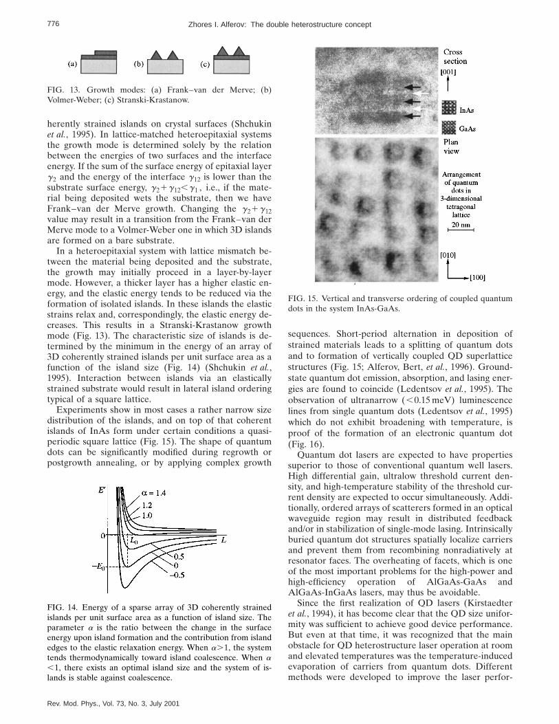
These groups came to the conclusion that the mostexciting method for forming ordered arrays of quantumwires and dots is use of self-organization phenomena oncrystal surfaces. Strain relaxation on step or facet edgesmay result in the formation of ordered arrays of quan-tum wires and dots for both lattice-matched and lattice-mismatched growth. The first very uniform arrays ofthree-dimensional quantum dots also exhibiting lateralordering were realized in the system InAs-GaAs by bothmolecular-beam epitaxy and metal-organic chemical-vapor deposition growth methods (Ledentsov et al.,1995; Alferov, Gordeev, et al., 1996).
Elastic strain relaxation on facet edges and island in-teraction via the strained substrate are driving forces forthe self-organization of ordered arrays of uniform, co-
FIG. 12. Normalized temperature dependence of the thresholdcurrent for various DHS lasers: (a) bulk; (b) with quantumwells; (c) with quantum wires; (d) with quantum dots.
776 Zhores I. Alferov: The double heterostructure concept
herently strained islands on crystal surfaces (Shchukinet al., 1995). In lattice-matched heteroepitaxial systemsthe growth mode is determined solely by the relationbetween the energies of two surfaces and the interfaceenergy. If the sum of the surface energy of epitaxial layerg2 and the energy of the interface g12 is lower than thesubstrate surface energy, g21g12,g1 , i.e., if the mate-rial being deposited wets the substrate, then we haveFrank–van der Merve growth. Changing the g21g12value may result in a transition from the Frank–van derMerve mode to a Volmer-Weber one in which 3D islandsare formed on a bare substrate.
In a heteroepitaxial system with lattice mismatch be-tween the material being deposited and the substrate,the growth may initially proceed in a layer-by-layermode. However, a thicker layer has a higher elastic en-ergy, and the elastic energy tends to be reduced via theformation of isolated islands. In these islands the elasticstrains relax and, correspondingly, the elastic energy de-creases. This results in a Stranski-Krastanow growthmode (Fig. 13). The characteristic size of islands is de-termined by the minimum in the energy of an array of3D coherently strained islands per unit surface area as afunction of the island size (Fig. 14) (Shchukin et al.,1995). Interaction between islands via an elasticallystrained substrate would result in lateral island orderingtypical of a square lattice.
Experiments show in most cases a rather narrow sizedistribution of the islands, and on top of that coherentislands of InAs form under certain conditions a quasi-periodic square lattice (Fig. 15). The shape of quantumdots can be significantly modified during regrowth orpostgrowth annealing, or by applying complex growth
FIG. 13. Growth modes: (a) Frank–van der Merve; (b)Volmer-Weber; (c) Stranski-Krastanow.
FIG. 14. Energy of a sparse array of 3D coherently strainedislands per unit surface area as a function of island size. Theparameter a is the ratio between the change in the surfaceenergy upon island formation and the contribution from islandedges to the elastic relaxation energy. When a.1, the systemtends thermodynamically toward island coalescence. When a,1, there exists an optimal island size and the system of is-lands is stable against coalescence.
Rev. Mod. Phys., Vol. 73, No. 3, July 2001
sequences. Short-period alternation in deposition ofstrained materials leads to a splitting of quantum dotsand to formation of vertically coupled QD superlatticestructures (Fig. 15; Alferov, Bert, et al., 1996). Ground-state quantum dot emission, absorption, and lasing ener-gies are found to coincide (Ledentsov et al., 1995). Theobservation of ultranarrow (,0.15 meV) luminescencelines from single quantum dots (Ledentsov et al., 1995)which do not exhibit broadening with temperature, isproof of the formation of an electronic quantum dot(Fig. 16).
Quantum dot lasers are expected to have propertiessuperior to those of conventional quantum well lasers.High differential gain, ultralow threshold current den-sity, and high-temperature stability of the threshold cur-rent density are expected to occur simultaneously. Addi-tionally, ordered arrays of scatterers formed in an opticalwaveguide region may result in distributed feedbackand/or in stabilization of single-mode lasing. Intrinsicallyburied quantum dot structures spatially localize carriersand prevent them from recombining nonradiatively atresonator faces. The overheating of facets, which is oneof the most important problems for the high-power andhigh-efficiency operation of AlGaAs-GaAs andAlGaAs-InGaAs lasers, may thus be avoidable.
Since the first realization of QD lasers (Kirstaedteret al., 1994), it has become clear that the QD size unifor-mity was sufficient to achieve good device performance.But even at that time, it was recognized that the mainobstacle for QD heterostructure laser operation at roomand elevated temperatures was the temperature-inducedevaporation of carriers from quantum dots. Differentmethods were developed to improve the laser perfor-
FIG. 15. Vertical and transverse ordering of coupled quantumdots in the system InAs-GaAs.

777Zhores I. Alferov: The double heterostructure concept
mance: (i) the increase of the density of quantum dotsby stacking them (Fig. 17); (ii) the insertion of quantumdots into a quantum well sheet; (iii) the use of a matrixmaterial with a higher band-gap energy. As a result, wegot many parameters of QD heterostructure lasers bet-ter than those for quantum well heterostructure lasersbased on the same materials. As an example, the world-record threshold current density of 19 A/cm2 was re-cently achieved (Park et al., 2000). Further, a cw outputpower up to 3.5–4.0 W (cw) for a 100-mm strip width, aquantum efficiency of 95% and a wall-plug efficiency of50% were recently obtained (Zhukov et al., 1999).
Significant efforts towards a theoretical understandingof QD lasers with realistic parameters have been under-taken. For a QD size dispersion of about 10% and other
FIG. 16. (a) High-resolution cathodoluminescence spectrum ofInAs-GaA; (b) temperature dependence of the full width athalf-maximum of the cathode peak.
FIG. 17. Transmission electron microscopy image of the activeregion of high-intensity laser.
Rev. Mod. Phys., Vol. 73, No. 3, July 2001
practical structure parameters, the theory (Asryan andSuris, 1996) predicts typical threshold current densitiesof 5 A/cm2 at room temperature. The values of 10 A/cm2
at 77 K (Zhukov et al., 1997) and even 5 A/cm2 at 4 K(Park et al., 1999) have been experimentally observed.
In view of advanced device applications of quantumdots, the incorporation of quantum dots in vertical-cavity surface-emitting lasers seems to be very impor-tant. QD vertical-cavity surface-emitting lasers with pa-rameters that fit to the best values for quantum welldevices of similar geometry have been demonstrated(Fig. 18; Lott et al., 1977). Recently, very promising re-sults have been obtained (Fig. 19; Lott et al., 2000) for1.3-mm QD vertical-cavity surface-emitting lasers on aGaAs substrate to use in fiber-optic communications.
In a free-standing 3D island formed on a lattice-mismatched substrate, the strains can relax elastically,without the formation of dislocations. Thus a sufficientlylarge volume of a coherent narrow-gap QD material canbe realized. This makes it possible to cover a spectral
FIG. 18. (a) Schematic view of the quantum dot vertical-cavitysurface-emitting laser structure. Basic advantages of quantumdots: (1) no interface recombination at oxide-defined aper-tures; (2) reduced lateral spreading of carriers out of the aper-ture region. Single quantum dot laser at ultralow thresholdcurrent is possible. (b) Dependence of the threshold current onthe aperture size in a QD vertical-cavity surface-emitting laser.(i) Low threshold current densities (170 A/cm2 at 300 K); (ii)low threshold currents at ultrasmall apertures; (iii) 1.3-mmrange on GaAs substrate.

778 Zhores I. Alferov: The double heterostructure concept
range of 1.3–1.5 mm using a GaAs substrate and to de-velop wavelength-multiplexing systems on the basis ofQD vertical-cavity surface-emitting lasers in the future.
It is very important to emphasize that we were able torealize the DHS concept for quantum wire and quantumdot structures because in both cases we have a narrowband-gap material in a wide-gap matrix.
Let us summarize again as we did for other parts.
HETEROSTRUCTURE QUANTUM WIRES AND DOTS
I. Fundamental physical phenomena
• 1D electron gas (wires)• Density-of-state function with sharp maximums
(wires)• 0D electron gas (dots)• d-function type of density-of-state function (dots)• Increasing binding energy of excitons
II. Important applications in electronics
• Reduced lasing threshold current and larger differ-ential gain
• Reduced temperature dependence of threshold cur-rent (wires)
• Temperature stability of the threshold current (dots)• Discrete amplification spectrum and a possibility of
obtaining performance characteristics similar to those ofsolid-state or gas lasers (dots)
• Higher modulation factor in electro-optical modula-tors
• Possibility of creating ‘‘single-electron’’ devices• A new possibility for the development of field-effect
transistors
III. Important technological peculiarities
• The application of self-organization effects forgrowth
• Epitaxial growth in V grooves (wires)• High-resolution lithography of heterostructure
quantum well lasers
V. FUTURE TRENDS
Recently very impressive results for short-wavelengthlight sources have been achieved on the basis of II-VI
FIG. 19. GaAs-based QD vertical-cavity surface-emitting laseremitting at 1.3 mm.
Rev. Mod. Phys., Vol. 73, No. 3, July 2001
selenides and III-V nitrides. The success in this researchwas mostly determined by the application of hetero-structure concepts and methods of growth which hadbeen developed for III-V quantum wells and superlat-tices. The natural and most predictable trend is the ap-plication of heterostructure concepts as well as techno-logical methods and peculiarities of new materials.Different III-V, II-VI, and IV-VI heterostructures,developed in recent times, are good examples of thisstatement.
But from a more fundamental point of view, hetero-structures (including quantum wells and superlattices,quantum wires, and quantum dots) offer a way to createnew types of materials—hetero-semiconductors. In thewords of Leo Esaki, instead of ‘‘God-made crystals’’ wecreate ‘‘man-made crystals.’’
The study of classical heterostructures, quantum wellsand superlattices is quite mature and we are now ex-ploiting many of their unique properties. The study ofquantum wire and dot structures is still very young: ex-citing discoveries and new unexpected applications areawaiting us. Even at this early stage, however, we cansay that ordered equilibrium arrays of quantum dotsmay be used in many devices: lasers, light modulators,far-infrared detectors and emitters, etc. Resonant tun-neling via semiconductor atoms introduced in largerband-gap layers may lead to significant improvement indevice characteristics. More generally speaking, QDstructures will be developed both ‘‘in width’’ and ‘‘indepth.’’
In width means new material systems to cover a newenergy spectrum. The lifetime limitations of the greenand blue semiconductor lasers and even more generalproblems of the creation of defect-free structures basedon wide-gap II-VI and III-V (nitrides) would be solvedby using QD structures in these systems.
As to in depth, it is necessary to mention that thedegree of ordering depends on very complicated growthconditions, materials constants, and concrete values ofthe surface free energy. To achieve resonant tunnelingand single-electron devices, including optical ones, re-quire a thorough investigation and evaluation of theseparameters in order to obtain the maximal possible de-gree of ordering. In general, it is necessary to find stron-ger self-organization mechanisms for ordered arrays ofquantum dots.
In the early 1980s I was invited to deliver a lectureabout heterostructures and applications at the AmocoPhotonic Center near Chicago.
The summary of my lecture was as follows:(1) Heterostructures—a new kind of semiconductor
material—expensive, complicated chemically and tech-nologically, but most efficient
(2) Modern optoelectronics is based on heterostruc-ture applications:
—The DHS laser—a key device of modern opto-electronics
—The heterostructure protodiode—the most effi-cient and high-speed photodiode

779Zhores I. Alferov: The double heterostructure concept
—Optoelectronic integrated circuits (OEIC’s)—willsolve problem of high information density of an opticalcommunication system
(3) Future high-speed microelectronics will mostlyuse heterostructures
(4) High-temperature, high-speed powerelectronics—a new broad field of heterostructure appli-cations
(5) Heterostructures in solar energy conversion: themost expensive photocells and the cheapest solar elec-tricity producer
(6) In the 21st century heterostructures in electronicswill reserve only 1% for homojunctions
And 20 years later I see no reason to change this sum-mary.
It is hardly possible to describe even the main direc-tions of modern physics and the technology of semicon-ductor heterostructures. There is much more than I havementioned. Many scientists contributed to this tremen-dous progress, which defines to a great extent not onlythe future prospects of condensed-matter physics andsemiconductor laser and communication technology, butalso, in a sense, the future of human society. I would likealso to emphasize the impact of scientists of previousgenerations who prepared our way. I am very happy thatI had a chance to work in this field from the very begin-ning. I am even happier that we can continue to contrib-ute to progress in this area now.
REFERENCES
Alferov, Zh. I., 1966, ‘‘Possible development of a rectifier forvery high current densities on the bases of a p-i-n(p-n-n1,n-p-p1) structure with heterojunctions,’’ Fiz. Tekh.Poluprovodn. 1, 436 [Sov. Phys. Semicond. 1, 358 (1967)].
Alferov, Zh. I., 1970, ‘‘Electroluminescence of heavily-dopedheterojunctions p AlxGa12x-nGaAs,’’ J. Lumin. 1, 869.
Alferov, Zh. I., et al., 1974, ‘‘Laser with supersmall divergenceof radiation,’’ Fiz. Tekh. Poluprovodn. 8, 832 [Sov. Phys.Semicond. 8, 541 (1974)].
Alferov, Zh. I., et al., 1975, ‘‘Semiconductor laser with distrib-uted feedback in second order,’’ Pis’ma Zh. Tekh. Fiz. 1, 645[Sov. Tech. Phys. Lett. 1, 286 (1975)].
Alferov, Zh. I., et al., 1985, ‘‘Auger-profiles and luminescenceinvestigations of LPE grown InGaAsP-heterostructures withactive regions (1.5–5)31026 cm,’’ Fiz. Tekh. Poluprovodn.19, 1108 [Sov. Phys. Semicond. 19, 679 (1985)].
Alferov, Zh. I., et al., 1986a, ‘‘AlGaAs-heterostructure quan-tum wells grown by low temperature LPE,’’ Pis’ma Zh. Tekh.Fiz. 12, 1089 [Sov. Tech. Phys. Lett. 12, 450 (1986)].
Alferov, Zh. I., et al., 1986b, ‘‘Low threshold InGaAsP/InPseparate confinement lasers l51.3 mm and l51.55 mm (j th
5600–700 A.cm2),’’ Pis’ma Zh. Tekh. Fiz. 12, 210 [Sov. Tech.Phys. Lett. 12, 87 (1986)].
Alferov, Zh. I., et al., 1987, ‘‘Low threshold quantum wellInGaAsP/GaAs separate confinement double heterostructurelasers formed by the LPE (l50.86 mm, j th590 A/cm2, L5` ; j th5165 A/cm2, L51150 mm, 300 K),’’ Fiz. Tekh. Polu-provodn. 21, 824 [Sov. Phys. Semicond. 21, 503 (1987)].
Alferov, Zh. I., et al., 1988a, ‘‘Quantum-well InGaAsP/GaAs(l50.86:0.78 mm) separate confinement lasers (j th
Rev. Mod. Phys., Vol. 73, No. 3, July 2001
5100 A/cm2, efficience559%),’’ Fiz. Tekh. Poluprovodn. 22,1031 [Sov. Phys. Semicond. 22, 650 (1988)].
Alferov, Zh. I., et al., 1988b, ‘‘Reducing of the threshold cur-rent in GaAs-AlGaAs DHS SCH quantum well lasers (j th
552 A/cm2, T5300 K) with quantum well restriction byshort period superlattice of variable period,’’ Pis’ma Zh.Tekh. Fiz. 14, 1803 [Sov. Tech. Phys. Lett. 14, 782 (1988)].
Alferov, Zh. I., F. A. Ahmedov, V. I. Korol’kov, and V. G.Nikitin, 1973, ‘‘Phototransistor utilizing a GaAs-AlAs hetero-junction,’’ Fiz. Tekh. Poluprovodn. 7, 1159 [Sov. Phys. Semi-cond. 7, 780 (1973)].
Alferov, Zh. I., V. M. Andreev, D. Z. Garbuzov, Yu. V. Zhi-lyaev, E. P. Morozov, E. L. Portnoi, and V. G. Trofim, 1970,‘‘Investigation of the influence of the AlAs-GaAs hetero-structure parameters on the laser threshold current and real-ization of continuous emission at room temperature,’’ Fiz.Tekh. Poluprovodn. 4, 1826 [Sov. Phys. Semicond. 4, 1573(1971)].
Alferov, Zh. I., V. M. Andreev, M. B. Kagan, I. I. Protasov, andV. G. Trofim, 1970, ‘‘Solar-energy converters based on p-nAlxGa12xAs-GaAs heterojunctions,’’ Fiz. Tekh. Polupro-vodn. 4, 2378 [Sov. Phys. Semicond. 4, 2047 (1971)].
Alferov, Zh. I., V. M. Andreev, R. F. Kazarinov, E. L. Portnoi,and R. A. Suris, 1971, ‘‘Semiconductor optical quantum gen-erator,’’ Inventor’s Certificate No. 392875 [in Russian], Appli-cation No. 1677436, priority as of July 19, 1971.
Alferov, Zh. I., V. M. Andreev, S. G. Konnikov, V. G. Nikitin,and D. N. Tret’yakov, 1971, ‘‘Heterojunctions on the base ofAIIIBV semiconducting and of their solid solutions,’’ in Pro-ceedings of the International Conference on Physics andChemistry of Semiconductor Heterojunctions and Layer Struc-tures, Budapest, October 1970, edited by G. Szigeti (Aca-demiai Kiado, Budapest), Vol. 1, p. 93.
Alferov, Zh. I., V. M. Andreev, V. I. Korol’kov, V. G. Nikitin,and A. A. Yakovenko, 1970, ‘‘p-n-p-n structures based onGaAs and on AlxGa12xAs solid solutions,’’ Fiz. Tekh. Polu-provodn. 4, 578 [Sov. Phys. Semicond. 4, 481 (1971)].
Alferov, Zh. I., V. M. Andreev, V. I. Korol’kov, E. L. Portnoi,and D. N. Tret’yakov, 1968a, ‘‘Injection properties ofn-AlxGa12xAs-p-GaAs heterojunctions,’’ Fiz. Tekh. Polu-provodn. 2, 1016 [Sov. Phys. Semicond. 2, 843 (1969)].
Alferov, Zh. I., V. M. Andreev, V. I. Korol’kov, E. L. Portnoi,and D. N. Tret’yakov, 1968b, ‘‘Coherent radiation of epitaxialheterojunction structures in the AlAs-GaAs system,’’ Fiz.Tekh. Poluprovodn. 2, 1545 [Sov. Phys. Semicond. 2, 1289(1969)].
Alferov, Zh. I., V. M. Andreev, V. I. Korol’kov, E. L. Portnoi,and D. N. Tret’yakov, 1969, ‘‘Recombination radiation in ep-itaxial structures in the system AlAs-GaAs,’’ in Proceedingsof the Ninth International Conference on SemiconductorStructures, Moscow, July 23–29, 1968 [in Russian] (Nauka,Leningrad), Vol. 1, p. 534.
Alferov, Zh. I., V. M. Andreev, V. I. Korol’kov, E. L. Portnoi,and A. A. Yakovenko, 1969a, ‘‘Recombination radiation inAlxGa12xAs solid solutions with variable forbidden gap,’’ Fiz.Tekh. Poluprovodn. 3, 541 [Sov. Phys. Semicond. 3, 460(1970)].
Alferov, Zh. I., V. M. Andreev, V. I. Korol’kov, E. L. Portnoi,and A. A. Yakovenko, 1969b, ‘‘Spontaneous radiationsources based on structures with AlAs-GaAs heterojunc-tions,’’ Fiz. Tekh. Poluprovodn. 3, 930 [Sov. Phys. Semicond.3, 785 (1970)].

780 Zhores I. Alferov: The double heterostructure concept
Alferov, Zh. I., V. M. Andreev, V. I. Korol’kov, D. N.Trat’yakov, and V. M. Tuchkevich, 1967, ‘‘High-voltage p-njunctions in GaxAl12xAs crystals,’’ Fiz. Tekh. Poluprovodn. 1,1579 [Sov. Phys. Semicond. 1, 1313 (1968)].
Alferov, Zh. I., V. M. Andreev, E. L. Portnoi, and M. K. Tru-kan, 1969, ‘‘AlAs-GaAs heterojunction injection lasers with alow room-temperature threshold,’’ Fiz. Tekh. Poluprovodn. 3,1328 [Sov. Phys. Semicond. 3, 1107 (1970)].
Alferov, Zh. I., I. N. Arsent’ev, D. Z. Garbuzov,S. G. Konnikov, and V. D. Rumyantsev, 1975a,‘‘Generation of coherent radiation in n Ga0.5 In0.5 P -p Gax;0.55 In1 2 x Asy;0.10 P1 2 y - n Ga0.5 In0.5 P , ’’ Pis’ma Zh.Tekh. Fiz. 1, 305 [Sov. Tech. Phys. Lett. 1, 147 (1975)].
Alferov, Zh. I., I. N. Arsent’ev, D. Z. Garbuzov, S. G. Konni-kov, and V. D. Rumyantsev, 1975b, ‘‘Red injection heterolas-ers in the Ga-In-As-P system,’’ Pis’ma Zh. Tekh. Fiz. 1, 406[Sov. Tech. Phys. Lett. 1, 191 (1975)].
Alferov, Zh. I., N. A. Bert, A. Yu. Egorov, A. E. Zhukov, P. S.Kop’ev, A. O. Kosogov, I. L. Krestnikov, N. N. Ledentsov, A.V. Lunev, M. V. Maksimov, A. V. Sakharov, V. M. Ustinov, A.F. Tsatsul’nikov, Yu. M. Shernyakov, and D. Bimberg, 1996,‘‘An injection heterojunction laser based on arrays of verti-cally coupled InAs quantum dots in a GaAs matrix,’’ Fiz.Tekh. Poluprovodn. 30, 351 [Sov. Phys. Semicond. 30, 194(1996)].
Alferov, Zh. I., D. Z. Garbuzov, V. S. Grigor’ev, Yu. V. Zhi-lyaev, L. V. Kradinova, V. I. Korol’kov, E. P. Morozov, O. A.Ninua, E. L. Portnoy, V. D. Prochukhan, and M. K. Trukan,1967, ‘‘Injection luminescence of epitaxial heterojunctions inthe GaP-GaAs system,’’ Sov. Phys. Solid State 9, 208.
Alferov, Zh. I., D. Z. Garbuzov, E. P. Morozov, and E. L. Port-noi, 1969, ‘‘Diagonal tunneling and polarization of radiationin AlxGa12xAs-GaAs heterojunctions and in GaAs p-n junc-tions,’’ Fiz. Tekh. Poluprovodn. 3, 1054 [Sov. Phys. Semicond.3, 885 (1970)].
Alferov, Zh. I., N. Yu. Gordeev, S. V. Zaitsev, P. S. Kop’ev, I. V.Kochnev, V. V. Khomin, I. L. Krestnikov, N. N. Ledentsov, A.V. Lunev, M. V. Maksimov, S. S. Ruvimov, A. V. Sakharnov,A. F. Tsatsul’nikov, Yu. M. Shernyakov, and D. Bimberg,1996, ‘‘A low-threshold injection heterojunction laser basedon quantum dots, produced by gas-phase epitaxy from orga-nometallic compounds,’’ Fiz. Tekh. Poluprovodn. 30, 357[Sov. Phys. Semicond. 30, 197 (1996)].
Alferov, Zh. I., and R. F. Kazarinov, 1963, ‘‘Semiconductor la-ser with electric pumping,’’ Inventor’s Certificate No. 181737[in Russian], Application No. 950840, priority as of March 30,1963.
Alferov, Zh. I., V. B. Khalfin, and R. F. Kazarinov, 1966, ‘‘Acharacteristic feature of injection into heterojunctions,’’ Fiz.Tverd. Tela 8, 3120 [Sov. Phys. Solid State 8, 2480 (1967)].
Alferov, Zh. I., Yu. V. Zhilyaev, and Yu. V. Shmartsev, 1971,‘‘The splitting of the conduction band in ‘superlattice’ on thebase GaPxAs12x , ’’ Fiz. Tekh. Poluprovodn. 5, 196 [Sov. Phys.Semicond. 5, 174 (1971)].
Anderson, R. L., 1960, ‘‘Germanium-gallium arsenide hetero-junctions,’’ IBM J. Res. Dev. 4, 283.
Anderson, R. L., 1962, ‘‘Experiments on Ge-GaAs heterojunc-tions,’’ Solid-State Electron. 5, 341.
Antipas, G. A., R. L. Moon, L. W. James, J. Edgecumbe, andR. L. Bell, 1973, ‘‘In gallium arsenide and related com-pounds,’’ Inst. Phys. Conf. Ser. 17, 48.
Arakawa, Y., and H. Sakaki, 1982, ‘‘Multidimensional quan-tum well laser and temperature dependence of its threshold
Rev. Mod. Phys., Vol. 73, No. 3, July 2001
current,’’ Appl. Phys. Lett. 40, 939.Asryan, L. V., and R. A. Suris, 1996, ‘‘Inhomogeneous line
broadening and the threshold current density of a semicon-ductor quantum dot laser,’’ Semicond. Sci. Technol. 11, 554.
Baranov, A. N., et al., 1986, ‘‘Generation of coherent radiationin quantum-sized structure of the single heterojunction,’’ Fiz.Tekh. Poluprovodn. 20, 2217 [Sov. Phys. Semicond. 20, 1385(1986)].
Basov, N. G., O. N. Krokhin, and Yu. M. Popov, 1961, ‘‘Thepossibility of use of indirect transitions to obtain negativetemperature in semiconductors,’’ Sov. Phys. JETP 12, 1033.
Blum, A. I., N. P. Mokrovsky, and A. R. Regel, 1952, ‘‘Thestudy of the conductivity of the semiconductors and interme-tallic compounds in solid and liquid state,’’ Izv. Akad. NaukSSSR, Ser. Fiz. 16, 139.
Bogatov, A. P., L. M. Dolginov, L. V. Druzhinina, P. G. Eliseev,L. N. Sverdlova, and E. G. Shevchenko, 1974, ‘‘Heterolaserson the base of solid solutions GaxIn12xAs4P12y andAlxGa12xSbyAs12y , ’’ Kvant. Elektron. 1, 2294 [Sov. J. Quan-tum Electron. 1, 1281 (1974)].
Chang, L. L., L. Esaki, W. E. Howard, and R. Ludke, 1973,‘‘Growth of GaAs-GaAlAs superlattices,’’ J. Vac. Sci. Tech-nol. 10, 11.
Chang, L. L., L. Esaki, and R. Tsu, 1974, ‘‘Resonant tunnelingin semiconductor double barriers,’’ Appl. Phys. Lett. 24, 593.
Cho, A. Y., 1971a, ‘‘Film deposition by molecular beam tech-niques,’’ J. Vac. Sci. Technol. 8, 31.
Cho, A. Y., 1971b, ‘‘Growth of periodic structures by themolecular-beam method,’’ Appl. Phys. Lett. 19, 467.
Davydov, B. I., 1939, ‘‘Contact resistance of semiconductors,’’Zh. Eksp. Teor. Fiz. 9, 451.
Delagebeaudeuf, D., et al., 1980, ‘‘Two-dimensional electrongas MESFET structure,’’ Electron. Lett. 16, 667.
Dingle, R., H. L. Stormer, H. L. Gossard, and W. Wiegmann,1978, ‘‘Electron mobilities in modulation-doped semiconduc-tor heterojunction superlattices,’’ Appl. Phys. Lett. 33, 665.
Dingle, R., W. Wiegmann, and C. H. Henry, 1974, ‘‘Quantizedstates of confined carriers in very thin AlxGa12xAs-GaAs-AlxGa12xAs heterostructures,’’ Phys. Rev. Lett. 33,827.
Dupuis, R. D., and P. D. Dapkus, 1977, ‘‘Room temperatureoperation of Ga12xAlxAs/GaAs double-heterostructure la-sers grown by metalorganic chemical vapor deposition,’’Appl. Phys. Lett. 31, 466.
Dupuis, R. D., P. D. Dapkus, N. Holonyak, Jr., E. A. Rezek,and R. Chin, 1978, ‘‘Room temperature operation ofquantum-well Ga12xAlxAs-GaAs laser diodes grown by met-alorganic chemical vapor deposition,’’ Appl. Phys. Lett. 32,295.
Ekimov, A. I., and A. A. Onushchenko, 1981, ‘‘Quantum sizeeffect in three dimensional microscopic semiconductor crys-tals,’’ JETP Lett. 34, 345.
Esaki, L., and L. L. Chang, 1974, ‘‘New transport phenomenonin a semiconductor ‘superlattice,’ ’’ Phys. Rev. Lett. 33, 686.
Esaki, L., and R. Tsu, 1970, ‘‘Superlattice and negative differ-ential conductivity,’’ IBM J. Res. Dev. 14, 61.
Faist, J., F. Capasso, D. L. Sivco, C. Sirtori, A. L. Hutchinson,and A. Y. Cho, 1994, ‘‘Quantum cascade laser,’’ Science 264,553.
Fowler, A. B., F. F. Fang, W. E. Howard, and P. J. Stiles, 1966,‘‘Magnetooscillatory conductance in silicon surfaces,’’ Phys.Rev. Lett. 16, 901.

781Zhores I. Alferov: The double heterostructure concept
Frenkel, Ya. I., 1931, ‘‘On the transformation of light into heatin solids,’’ Phys. Rev. 37, 17; 37, 1276.
Frenkel, Ya. I., 1936, ‘‘Light absorption and electrons andholes sticking in dielectric crystals,’’ Zh. Eksp. Teor. Fiz. 6,647.
Frenkel, Ya. I., and A. Ioffe, 1932, ‘‘On the electrical and pho-toelectric properties of contacts between a metal and semi-conductor,’’ Phys. Z. Sowjetunion 1, 60.
Garbuzov, D. Z., et al., 1988, ‘‘Technical Digest CLEO,’’ PaperTHU44, p. 396.
Garbuzov, D. Z., et al., 1990, Conference Digest 12th Interna-tional Semiconductor Laser Conference, Davos, Switzerland,Paper L-33, p. 238.
Goldschmidt, V. M., 1929, ‘‘Crystal structure and chemical con-stitution,’’ Trans. Faraday Soc. 25, 253.
Goldstein, L., F. Glas, J. Y. Marzin, M. N. Charasse, and G. LeRoux, 1985, ‘‘Growth by molecular beam epitaxy and charac-terization of InAs/GaAs strained-layer superlattices,’’ Appl.Phys. Lett. 47, 1099.
Goryunova, N. A., 1951, ‘‘Seroe olovo’’ [Gray tin], Thesis(Leningrad State University, Physico-Technical Institute).
Gross, E. F., and N. A. Karryev, 1952a, ‘‘Light absorption bycuprous oxide crystal in infrared and visible spectrum,’’ Dokl.Akad. Nauk SSSR 84, 261.
Gross, E. F., and N. A. Karryev, 1952b, ‘‘Exciton optical spec-trum,’’ Dokl. Akad. Nauk SSSR 84, 471.
Gubanov, A. I., 1950, ‘‘Theory of the contact between twosemiconductors with different types of conduction,’’ Zh.Tekh. Fiz. 20, 1287.
Gubanov, A. I., 1951, ‘‘Theory of the contact of two semicon-ductors of the same type of conductivity,’’ Zh. Tekh. Fiz. 21,304.
Hall, R. H., G. E. Fenner, J. D. Kingsley, T. J. Soltys, and R. O.Carlson, 1962, ‘‘Coherent light emission from GaAs junc-tion,’’ Phys. Rev. Lett. 9, 366.
Hayashi, I., 1984, ‘‘Heterostructure lasers,’’ IEEE Trans. Elec-tron Devices ED-31, 1630.
Hayashi, I., M. B. Panish, P. W. Foy, and S. Sumski, 1970,‘‘Junction lasers which operate continuously at room tem-perature,’’ Appl. Phys. Lett. 17, 109.
Hitchens, W. R., N. Holonyak, Jr., P. D. Wright, and J. J. Cole-man, 1975, ‘‘Low-threshold LPE In12x8Gax8P12z8Asz8 /In12xGaxP12zAsz /In12x8Gax8P12z8Asz8 yellow double-heterojunction laser diodes (J,104 A/cm2, I55850 A, 77K),’’ Appl. Phys. Lett. 27, 245.
Holonyak, N., Jr., and S. F. Bevacgua, 1962, ‘‘Coherent (vis-ible) light emission from Ga(As12xPx) junctions,’’ Appl.Phys. Lett. 1, 83.
Hsieh, J. J., 1976, ‘‘Room-temperature operation GaInAsP/InPdouble-heterostructure diode lasers emitting at 1.1 mm,’’Appl. Phys. Lett. 28, 283.
James, L., G. Antipas, R. Moon, J. Edgecumbe, and R. L. Bell,1973, ‘‘Photoemission from cesium-oxide-activated In-GaAsP,’’ Appl. Phys. Lett. 22, 270.
Kazarinov, R. F., and R. A. Suris, 1971, ‘‘Possibility of the am-plification of electromagnetic waves in a semiconductor witha superlattice,’’ Fiz. Tekh. Poluprovodn. 5, 797 [Sov. Phys.Semicond. 5, 707 (1971)].
Kazarinov, R. F., and R. A. Suris, 1972a, ‘‘Electric and electro-magnetic properties of semiconductors with a superlattice,’’Fiz. Tekh. Poluprovodn. 6, 148 [Sov. Phys. Semicond. 6, 120(1972)].
Rev. Mod. Phys., Vol. 73, No. 3, July 2001
Kazarinov, R. F., and R. A. Suris, 1972b, ‘‘Injection heterolaserwith diffraction grating on contact surface,’’ Fiz. Tekh. Polu-provodn. 6, 1359 [Sov. Phys. Semicond. 6, 1184 (1973)].
Kazarinov, R. F., and R. A. Suris, 1973, ‘‘Theory of electricalproperties of semiconductors with superlattices,’’ Fiz. Tekh.Poluprovodn. 7, 488 [Sov. Phys. Semicond. 7, 347 (1973)].
Keldysh, L. V., 1962, ‘‘Effect of ultrasonics on the electronspectrum of crystals,’’ Fiz. Tverd. Tela. 4, 2265 [Sov. Phys.Semicond. 4, 1658 (1963)].
Kirstaedter, N., et al., 1994, ‘‘Low threshold, large T0 injectionlaser emission from (InGa)As quantum dots,’’ Electron. Lett.30, 1416.
Klitzing, K. V., G. Dorda, and M. Pepper, 1980, ‘‘New methodfor high-accuracy determination of the fine-structure constantbased on quantized Hall resistance,’’ Phys. Rev. Lett. 45, 494.
Kogelnik, H., and C. V. Shank, 1971, ‘‘Stimulated emission in aperiodic structure,’’ Appl. Phys. Lett. 18, 152.
Kroemer, H., 1957a, ‘‘Theory of a wide-gap emitter for transis-tors,’’ Proc. IRE 45, 1535.
Kroemer, H. 1957b, ‘‘Quasi-electric and quasi-magnetic fieldsin a non-uniform semiconductor,’’ RCA Rev. 28, 332.
Kroemer, H., 1963, ‘‘A proposed class of heterojunction injec-tion lasers,’’ Proc. IEEE 51, 1782.
Kroemer, H., and G. Griffiths, 1983, ‘‘Staggered-lineup hetero-junctions as sources of tunable below-gap radiation: Operat-ing principle and semiconductor selection,’’ IEEE ElectronDevice Lett. EDL-4, 1, 20.
Ledentsov, N. N., M. Grundmann, N. Kirstaedter, J. Christen,R. Heitz, J. Bohrer, F. Heinrichsdorff, D. Bimberg, S. S. Ru-vimov, P. Werner, U. Richter, U. Gosele, J. Heydenreich, V.M. Ustinov, A. Yu. Egorov, M. V. Maximov, P. S. Kop’ev, andZh. I. Alferov, 1995, ‘‘Luminescence and structural propertiesof (In,Ga)As-GaAs quantum dots,’’ in Proceedings of the22nd International Conference on the Physics of Semiconduc-tors, Vancouver, Canada, 1994, edited by D. J. Lockwood(World Scientific, Singapore), Vol. 3, p. 1855.
Lott, J. A., N. N. Ledentsov, V. M. Ustinov, A. Yu. Egorov, A.E. Zhukov, P. S. Kop’ev, Zh. I. Alferov, and D. Bimberg,1997, ‘‘Vertical cavity lasers based on vertically coupled quan-tum dots,’’ Electron. Lett. 33, 1150.
Lott, J. A., N. N. Ledentsov, V. M. Ustinov, N. A. Maleev, A.E. Zhukov, A. R. Kovsh, M. V. Maximov, B. V. Volovik, Zh. I.Alferov, and D. Bimberg, 2000, ‘‘InAs-InGaAs quantum dotVCSELs on GaAs substrates emitting at 1.3 mm,’’ Electron.Lett. 36, 1384.
Ludowise, M., W. T. Dietze, C. K. Lewis, M. D. Camras, N.Holonyak, Jr., B. K. Fuller, and M. A. Nixon, 1983, ‘‘Continu-ous 300 K laser operation of strained superlattices,’’ Appl.Phys. Lett. 42, 487.
Lutskii, V. N., 1970, ‘‘Quantum-size effect-present state andperspective on experimental investigations,’’ Phys. Status So-lidi A 1, 199.
Manasevit, H. M., 1968, ‘‘Single crystal GaAs on insolatingsubstrates,’’ Appl. Phys. Lett. 12, 156.
Mimura, T., S. Hiyamizu, T. Fuji, and K. Nanbu, 1980, ‘‘A newfield-effect transistor with selectively dopedGaAs/n-AlxGa12xAs heterojunctions,’’ Jpn. J. Appl. Phys.19, L225.
Nakamura, M., A. Yariv, H. W. Yen, S. Somekh, and H. L.Garvin, 1973, ‘‘Optically pumped GaAs surface laser withcorrugation feedback,’’ Appl. Phys. Lett. 22, 315.
782 Zhores I. Alferov: The double heterostructure concept
Nasledov, D. N., A. A. Rogachev, S. M. Ryvkin, and B. V.Tsarenkov, 1962, ‘‘Recombination radiation of galiun ar-senic,’’ Fiz. Tverd. Tela 4, 1062 [Sov. Phys. Solid State 4, 782(1962)].
Nathan, M. I., W. P. Dumke, G. Burns, F. H. Dill, Jr., and G. I.Lasher, 1962, ‘‘Stimulated emission of radiation from GaAsp-n junctions,’’ Appl. Phys. Lett. 1, 62.
Natta, G., and L. Passerini, 1928, Gazz. Chim. Ital. 58, 458.Osbourn, G., 1982, ‘‘Strained-layer superlattices from lattice
mismatched materials,’’ J. Appl. Phys. 53, 1586.Park, G., O. B. Shchekin, S. Csutak, D. L. Huffaker, and D.
Deppe, 1999, ‘‘Room-temperature continuous-wave opera-tion of a single-layered 1.3 mm quantum dot laser,’’ Appl.Phys. Lett. 75, 3267.
Park, G., O. B. Shchekin, D. L. Huffaker, and D. G. Deppe,2000, ‘‘Low threshold oxide-confined 1.3 mm quantum dotlaser,’’ IEEE Photonics Technol. Lett. 33, 230.
Rezek, E., H. Shichijo, B. A. Vojak, and N. Holonyak, 1977,‘‘Confined-carrier luminescence of a thin In12xGaxP12zAsz
well (x0;0.13, z;0.29, ;400 A) in an InP p-n junction,’’Appl. Phys. Lett. 31, 534.
Rupprecht, H. S., J. M. Woodall, and G. D. Pettit, 1967, ‘‘Ef-ficient visible electroluminescence at 300 K from Ga12xAlxAsp-n junctions grown by liquid-phase epitaxy,’’ Appl. Phys.Lett. 11, 81.
Scifres, D. R., R. D. Burnham, and W. Streifer, 1974,‘‘Distributed-feedback single heterojunction GaAs diode la-ser,’’ Appl. Phys. Lett. 25, 203.
Shchukin, V. A., N. N. Ledentsov, P. S. Kop’ev, and D. Bim-berg, 1995, ‘‘Spontaneous ordering of arrays of coherentstrained islands,’’ Phys. Rev. Lett. 75, 2968.
Shockley, W., 1951, ‘‘Circuit element utilizing semiconductormaterial,’’ U.S. Patent 2269347, September 25.
Shriffer, J. R., 1957, ‘‘Semiconductor surface physics,’’ in Pro-
Rev. Mod. Phys., Vol. 73, No. 3, July 2001
ceedings of the Conference on the Physics of SemiconductorSurfaces, Philadelphia, June 1956, edited by R. H. Kingston(University of Pennsylvania, Philadelphia), p. 68.
Tsang, W. T., 1982, ‘‘Extremely low threshold (AlGa)Asgraded-index waveguide separate-confinement heterostruc-ture lasers grown by molecular-beam epitaxy,’’ Appl. Phys.Lett. 40, 217.
Tsu, R., and L. Esaki, 1973, ‘‘Tunneling in finite superlattice,’’Appl. Phys. Lett. 22, 562.
Tsui, D. C., H. L. Stormer, and A. C. Gossard, 1982, ‘‘Twodimensional magnetotransport in the extreme quantumlimit,’’ Phys. Rev. Lett. 48, 1559.
van der Ziel, J. P., R. Dingle, R. C. Miller, W. Wiegmann, andW. A. Nordland, Jr., 1975, ‘‘Laser oscillations from quantumstates in very thin GaAs-Al0.2Ga0.8As multilayer structures,’’Appl. Phys. Lett. 26, 463.
Welker, N. H., 1939, ‘‘Uber neue halblestende Verbindungen’’[New semiconductor compounds], Z. Naturforsch. A 7a, 744;1953, Z. Naturforcsch A 8a, 248.
Zhukov, A. E., A. R. Kovsh, S. S. Mikhrin, N. A. Maleev, V. M.Ustinov, D. A. Lifshits, I. S. Tarasov, D. A. Bedarev, M. V.Maximov, A. F. Tsatsul’nikov, I. P. Soshnikov, P. S. Kop’ev,Zh. I. Alferov, N. N. Ledentsov, and D. Bimberg, 1999, ‘‘3.9W CW power from submonolayer quantum dot diode laser,’’Electron. Lett. 35, 1845.
Zhukov, A. E., V. M. Ustinov, A. Yu. Egorov, A. R. Kovsh, A.F. Tsatsul’nikov, N. N. Ledenstov, S. V. Zaitsev, N. Yu.Gordeev, P. S. Kop’ev, and Zh. I. Alferov, 1997, ‘‘Negativecharacteristic temperature of InGaAs quantum dot injectionlaser,’’ Jpn. J. Appl. Phys., Part 1 36, 4216.
Zhuze, V. P., and I. V. Kurchatov, 1932a, ‘‘To question aboutconductivity of cuprous oxide,’’ Zh. Eksp. Teor. Fiz. 2, 309.
Zhuze, V. P., and I. V. Kurchatov, 1932a, ‘‘Zur electrischen Le-itfahigkeit von Kupferoxydul,’’ Phys. Z. Sowjetunion 2, 453.