Embed Size (px)
Citation preview

All Rights Reserved, Copyright FUJITSU Advanced Technologies Ltd., 20080
Noise Countermeasure Design Technologyfor Signal and Power Integrity
[IBIS Summit Tokyo, Japan November 14, 2008]
November 14,2008
Toshiro SatoCircuit Technology Development Div.FUJITSU Advanced Technologies Ltd.

All Rights Reserved, Copyright FUJITSU Advanced Technologies Ltd., 2008 1
INDEX
1. Background2. Tasks3. Countermeasures4. LSI,PCB Unified Noise Analysis5. Application Results6. Conclusions7. Future Tasks

All Rights Reserved, Copyright FUJITSU Advanced Technologies Ltd., 2008 2
Speed Up of Operating Frequency
1. Background
0.01
0.1
1
10
1995 2000 2005 2010
SDRAM
DDRDDR2
DDR3AGP
FibreChannel
PCI-ePCI-e Gen2
Parallel Transmission
Serial Transmission
YEAR
Dat
a R
ate
[G
bps/
ch]
XFI/10GbE
130nm 65nm180nm250nm 90nm350nm Process
All Rights Reserved, Copyright FUJITSU Advanced Technologies Ltd., 2008 3
1. Background
図2 電源電圧と消費電流トレンド
0
50
100
150
200
250
2003 2004 2005 2006 2007 2008 2009
Gat
e Le
ngth
[nm
]Po
wer
Con
sum
ptio
n[W
]Cu
rren
t Co
nsum
ptio
n[A
]
1.3
1.1
1.0
0.9
0.8
1.2
Supp
ly V
olta
ge[V
]
Supply Voltage
Power Consumption
Gate Length
(YEAR)
Current Consumption
ITRS2004
Lowering of Supply Voltage
Supply voltage : Lowering Allowable power noise : SmallerSupply voltage : Lowering Allowable power noise : Smaller

All Rights Reserved, Copyright FUJITSU Advanced Technologies Ltd., 2008 4
1. Signal Integrity(SI)(1) Reflection noise,Crosstalk noise(2) Skin effect、Dielectric loss(3) ISI:Inter Symbol Interference
2. Power Integrity (PI, power noise)(1) Simultaneous switching noise(2) Voltage and ground bounce noise(3) Noise caused by return current
3. EMC(1) EMI(2) ESD
4.Composite Noise Complex noise problems composed of SI,PI and EMI/ESD etc..Ex. Deterioration of cell phone antenna sensitivity
Emerging of Noise Problem
2. Tasks

All Rights Reserved, Copyright FUJITSU Advanced Technologies Ltd., 2008 5
Floor Plan based AnalysysFloor Plan based Floor Plan based AnalysysAnalysysSimulation based Design
Signal IntegritySignal Integrity
Power IntegrityPower Integrity
EMC(EMI,ESD)EMC(EMI,ESD)
Full automaticverificationFull automaticverification
Advice for design condition
Advice for design condition
Multi-Gbpsanalysis
Multi-Gbpsanalysis
Middlescale
Middlescale
LargescaleLargescale
EMI EMI ESDReturn Current
ESDReturn Current
1995 2000 2005NOW▼
LSI,PCB UnifiedAnalysis
TechnicalComputing
・Large Scale Analysis・high Speed Analysis
Unified AnalysisEnviornmemt
LSI Power Noise Analysis
LSI Power Noise Analysis
3. Countermeasures
DriverLSI
PCBV/G Noise
LSI core noise IO SSO noise
EMIfrom
V/G Layer
EMIfrom
Signal Pattern
PKG
ReceiverLSI
PCB
mutual Interference
DriverLSI
PCBV/G Noise
LSI core noise IO SSO noise
EMIfrom
V/G Layer
EMIfrom
Signal Pattern
PKG
ReceiverLSI
PCB
mutual Interference

All Rights Reserved, Copyright FUJITSU Advanced Technologies Ltd., 2008 6
LSI
Supply Current:Ip(t)
V
G
Decoupling Capacitor
Voltage Supply
Z(f)
V/G Plane
ΔV(t)
・Power noise :ΔV=-Z(f) ×△Ip・V/G Impedance :Z(f)≦ΔVmax/△Ip = Allowable Impedance
Ip(t)
Ip(t)
Occurring principle of Power noise
4. LSI,PCB Unified Noise Analysis
Equivalent Circuit of LSI,PCB and voltage supply

All Rights Reserved, Copyright FUJITSU Advanced Technologies Ltd., 2008 7
V/G impedance Allowable impedance
Frequency[Hz]
Impe
dan
ce[Ω
]High accuracy power noise analysis High accuracy power noise analysis
Tasks
Suppressing V/G impedanceunder the allowable impedance
become more difficult
Allowable impedance decreasingcaused by frequency increasingand supply voltage decreasing
High accuracy power noise analysismethod is required
4. LSI,PCB Unified Noise Analysis

All Rights Reserved, Copyright FUJITSU Advanced Technologies Ltd., 2008 8
ΔVp(f)
Voltagesupply
Decoupling capacitor
PCB
PKG
G
V
Ip(f)
Zp(f)
LSI core
ΔVp(f)
Voltagesupply
Decoupling capacitor
PCB
PKG
G
V
Ip(f)
Zp(f)
LSI core
LSI,PCB Unified Noise AnalysisLSI,PCB Unified Noise Analysis
LSI
4. LSI,PCB Unified Noise Analysis
Tasks
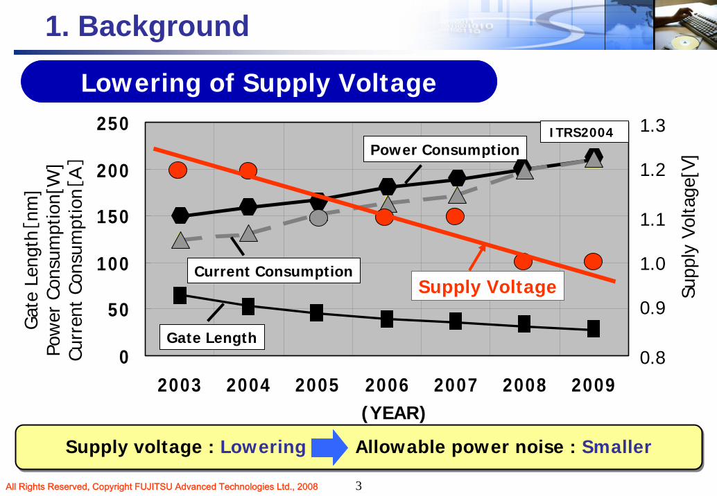
More Detailed Equivalent Circuit of LSI,PCB and voltage supply
All Rights Reserved, Copyright FUJITSU Advanced Technologies Ltd., 2008 9
1K 10K 100K 1M 10M 100M 1G
10
1
100m
10m
1m
0.1m
Frequency(Hz)
Zp(Ω
)
1K 10K 100K 1M 10M 100M 1G
10
1
100m
10m
1m
0.1m
10
1
100m
10m
1m
0.1m
Frequency(Hz)
Zp(Ω
) Using PCB modelUsing LSI model
Using LSI and PCB model②、③models have large calculation error
LSI,PCB unified model is essential for high accuracy
4. LSI,PCB Unified Noise Analysis
LSI,PCB Unified Noise AnalysisLSI,PCB Unified Noise AnalysisTasks

All Rights Reserved, Copyright FUJITSU Advanced Technologies Ltd., 2008 10
Delay variation of signal and clock Split clock waveform
tpdtpd+Δt
tpd-Δt Signal waveform
Power noise
Vth
Delay variation
Vth
Waveform split by power noise
SI and PI Problem should be solved simultaneously SI and PI Problem should be solved simultaneously
4. LSI,PCB Unified Noise Analysis
TasksLSI,PCB Unified Noise AnalysisLSI,PCB Unified Noise Analysis

All Rights Reserved, Copyright FUJITSU Advanced Technologies Ltd., 2008 11
System configuration
Power Noise AnalysisSystem
Device CharacteristicDefinition
PCB CAD Data
Layout CAD Data ConverterFloor PlannerLSI model Generation
Purchased LSI ModelVoltage Supply DeviceCondenserIntra-LSI Model
EMI Solver
Calculated EMI
Power Noise WaveformV/G Impedance1.0E-02
1.0E-01
1.0E+00
1.0E+08 1.0E+09
周波数[Hz]
イン
ピー
ダン
ス[Ω
]
対策前 対策後 目標インピーダンス
LSI,PCB Unified Model
Other Layout CAD
Circuit Simulator
4. LSI,PCB Unified Noise Analysis

All Rights Reserved, Copyright FUJITSU Advanced Technologies Ltd., 2008 12
LSI,PCB Unified model
PCB
LSI core:Distributed current Source
Intra-LSI V/G:Lattice of LCR SPICE model
IO cell:SPICE modelBehavior model
Package:LCR model
V/G Pin:LCR model
・・・
LSI made by FUJITSU
Board V/G:LCR Mesh model
Bypass condenser(C, ESL, ESR)Draw out wiring
V-Layer
G-Layer
Wiring/via:LCR ladder model
Purchased LSI:IBIS model(IO Model,PKG)
4. LSI,PCB Unified Noise Analysis
IBIS models not suitablefor power noise analysis
IBIS models not suitablefor power noise analysis
All Rights Reserved, Copyright FUJITSU Advanced Technologies Ltd., 2008
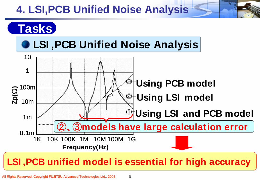
High Speed Transmission Waveform Simulation with Power noise
Eye pattern diagram
Transmission waveform simulatorTransmission waveform simulator
IO model・SPICE ・Behavior
W-element model
4. LSI,PCB Unified Noise Analysis
Power Noise Waveformscalculated by LSI,PCB Unified Analysis
Added to V/G pins of IO models
This method significantly shortens the calculation time comparing to the full LSI,PCB Unified Analysis with the comparable accuracy.This method significantly shortens the calculation time comparing to the full LSI,PCB Unified Analysis with the comparable accuracy.
IBIS models not suitablefor such a method
13
All Rights Reserved, Copyright FUJITSU Advanced Technologies Ltd., 2008 14
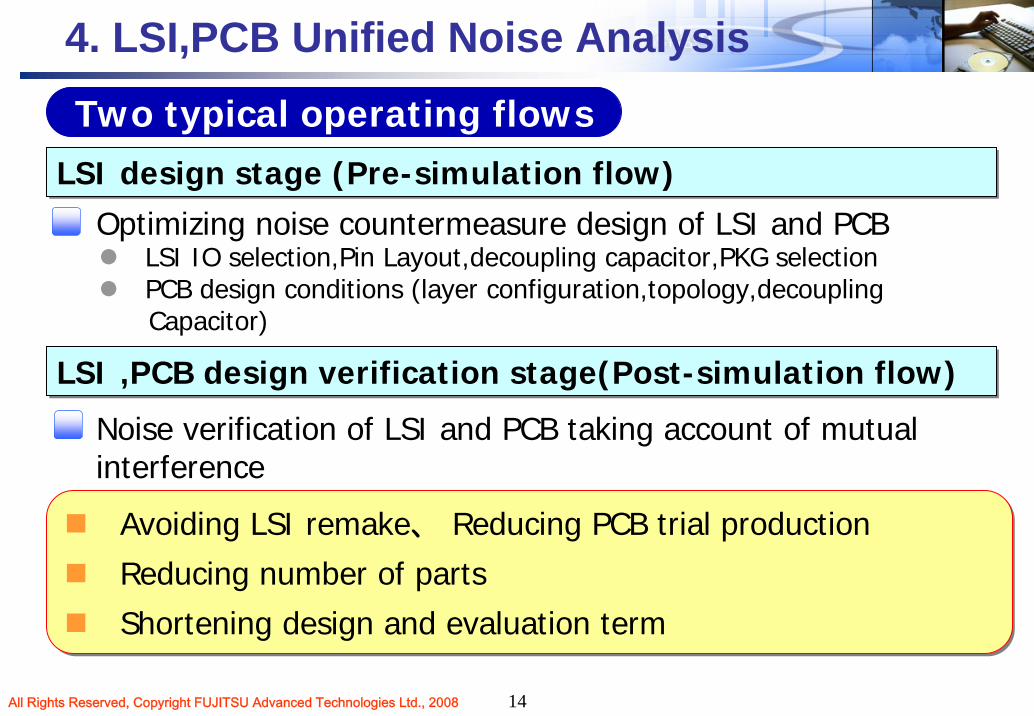
Avoiding LSI remake、 Reducing PCB trial production
Reducing number of parts
Shortening design and evaluation term
Avoiding LSI remake、 Reducing PCB trial production
Reducing number of parts
Shortening design and evaluation term
Optimizing noise countermeasure design of LSI and PCB
Two typical operating flows
LSI design stage (Pre-simulation flow)LSI design stage (Pre-simulation flow)
LSI IO selection,Pin Layout,decoupling capacitor,PKG selectionPCB design conditions (layer configuration,topology,decouplingCapacitor)
LSI ,PCB design verification stage(Post-simulation flow)LSI ,PCB design verification stage(Post-simulation flow)
Noise verification of LSI and PCB taking account of mutual interference
4. LSI,PCB Unified Noise Analysis
All Rights Reserved, Copyright FUJITSU Advanced Technologies Ltd., 2008 15
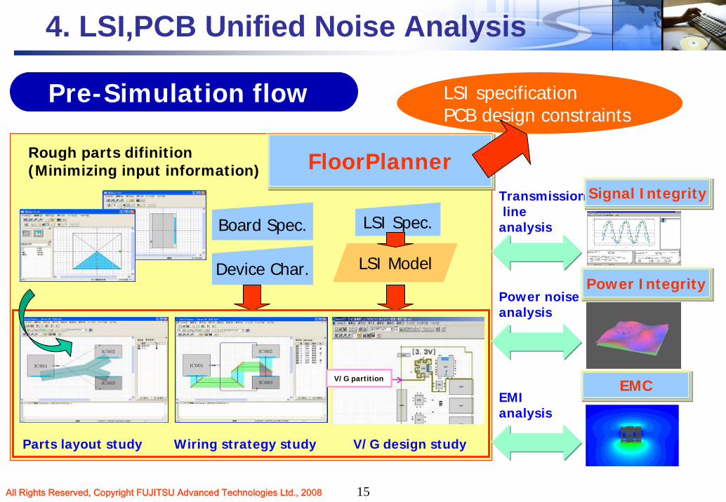
Rough parts difinition(Minimizing input information)
Parts layout study Wiring strategy study
Pre-Simulation flow
Transmissionline
analysis
EMIanalysis
LSI ModelDevice Char.
Board Spec.
FloorPlannerFloorPlanner
Power IntegrityPower Integrity
Signal IntegritySignal Integrity
EMCEMC
V/G design study
LSI specificationPCB design constraints
Power noiseanalysis
LSI Spec.
V/G partition
4. LSI,PCB Unified Noise Analysis
All Rights Reserved, Copyright FUJITSU Advanced Technologies Ltd., 2008 16
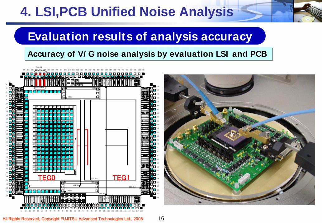
TPA9V5(CS90A、4mm□)
TEG1TEG0
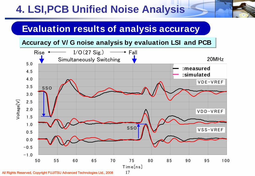
Accuracy of V/G noise analysis by evaluation LSI and PCB Accuracy of V/G noise analysis by evaluation LSI and PCB
Evaluation results of analysis accuracy
4. LSI,PCB Unified Noise Analysis
All Rights Reserved, Copyright FUJITSU Advanced Technologies Ltd., 2008 17
FallRise I/O(27 Sig.)Simultaneously Switching 20MHz
-1.0
-0 .5
0 .0
0 .5
1 .0
1 .5
2 .0
2 .5
3 .0
3 .5
4 .0
4 .5
5 .0
50 55 60 65 70 75 80 85 90 95 100
T im e[ns]
Vol
tage
[V]
黒 : 実 測赤 : TC S Sim .結 果
VDE-VREF
VDD-VREF
VSS-VREFSSO
SSO
Accuracy of V/G noise analysis by evaluation LSI and PCB Accuracy of V/G noise analysis by evaluation LSI and PCB
Evaluation results of analysis accuracy
:measured:simulated
4. LSI,PCB Unified Noise Analysis
All Rights Reserved, Copyright FUJITSU Advanced Technologies Ltd., 2008 18
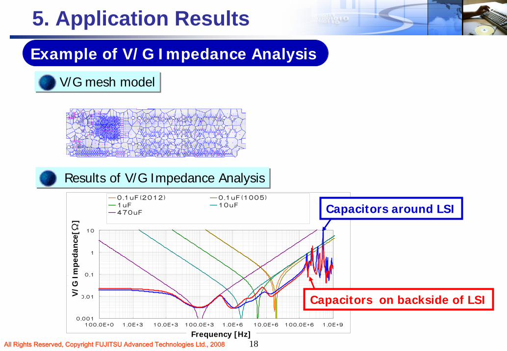
Example of V/G Impedance Analysis
5. Application Results
0 .0 0 1
0 .0 1
0 .1
1
1 0
1 0 0 .0 E + 0 1 .0 E + 3 1 0 .0 E + 3 1 0 0 .0 E + 3 1 .0 E + 6 1 0 .0 E + 6 1 0 0 .0 E + 6 1 .0 E + 9周 波 数 [ H z]
イン
ピー
ダン
ス[
Ω]
0 .1 uF (2 0 1 2 ) 0 .1 uF (1 0 0 5 )
1 uF 1 0 uF
4 7 0 uF
① L S I周 辺 に パ ス コ ン を 配 置 ② L S I裏 面 に パ ス コ ン を 配 置
V/G
Im
peda
nce
[Ω]
Frequency [Hz]
V/G mesh modelV/G mesh model
Results of V/G Impedance Analysis Results of V/G Impedance Analysis
Capacitors around LSI
Capacitors on backside of LSI
All Rights Reserved, Copyright FUJITSU Advanced Technologies Ltd., 2008 19
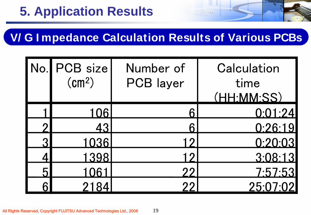
1 106 6 0:01:242 43 6 0:26:193 1036 12 0:20:034 1398 12 3:08:135 1061 22 7:57:536 2184 22 25:07:02
No. PCB size(㎝2)
Number ofPCB layer
Calculationtime
(HH:MM:SS)
5. Application Results
V/G Impedance Calculation Results of Various PCBs

All Rights Reserved, Copyright FUJITSU Advanced Technologies Ltd., 2008 20
【【Using Layout CAD DataUsing Layout CAD Data】】【【Using Floor Planner CAD Data Using Floor Planner CAD Data 】】
Analysis ModelAnalysis Model
PCB size(c㎡)
Number ofPCB layer
180 10
【Specification of Analyzed PCB】
5. Application Results
V/G Impedance Analysis Using Floor Planner

All Rights Reserved, Copyright FUJITSU Advanced Technologies Ltd., 2008 21
Calculation TimeCalculation TimeAnalysis ResultAnalysis Result
Calculation Time
50MB
Model Size((HH:MM:SS)HH:MM:SS)
2MBFloor Planner
x180 faster
電源インピーダンスの周波数特性
Floor Planner DataLayout CAD Data
Good Accordance
Power noise countermeasure from floor planning stage enables us to easily determine Power design constraint.
(Decoupling capacitors,V/G layer construction,V/G layer partition)
Power noise countermeasure from floor planning stage enables us to easily determine Power design constraint.
(Decoupling capacitors,V/G layer construction,V/G layer partition)
5. Application ResultsV
/G I
mpe
dan
ce[Ω
]
Frequency [Hz]
Results of V/G Impedance Analysis CAD Data
Layout CAD0:01:374:52:00
V/G Impedance Analysis Using Floor Planner
All Rights Reserved, Copyright FUJITSU Advanced Technologies Ltd., 2008
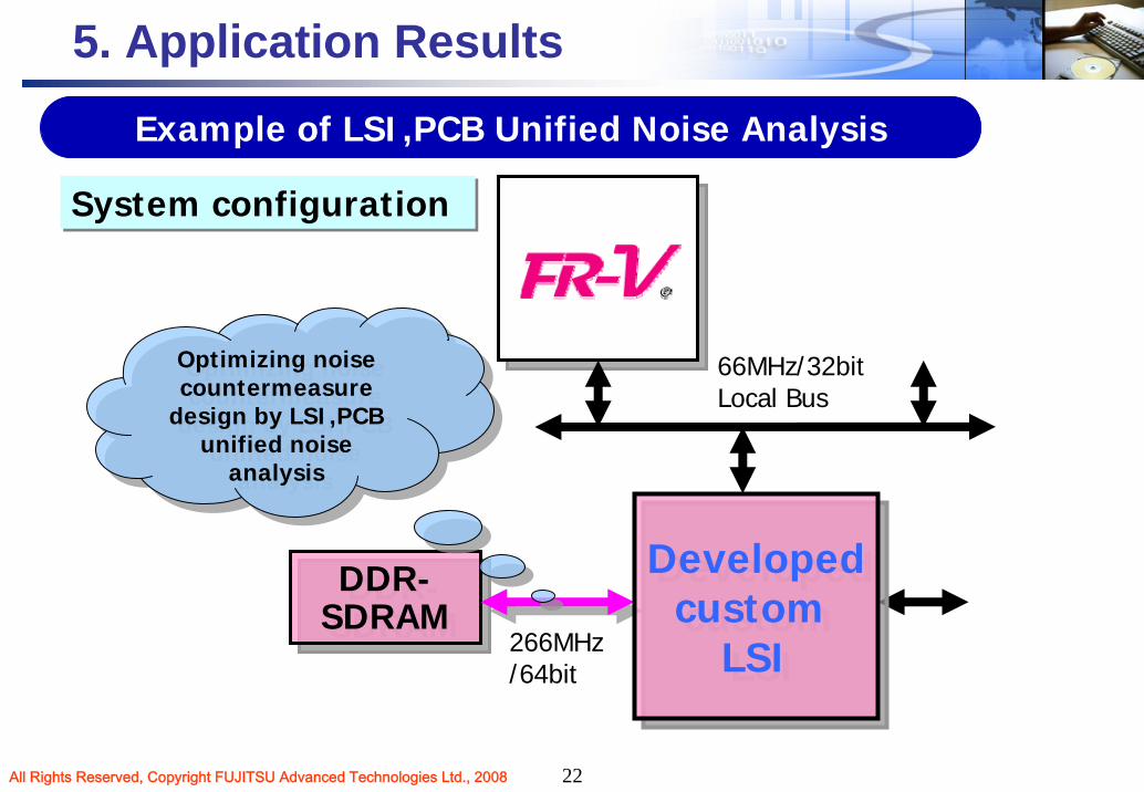
66MHz/32bitLocal Bus
266MHz/64bit
DDR-SDRAMDDR-
SDRAMDeveloped
custom LSI
Developedcustom
LSI
Optimizing noise countermeasure
design by LSI,PCB unified noise
analysis
Optimizing noise countermeasure
design by LSI,PCB unified noise
analysis
System configurationSystem configuration
Example of LSI,PCB Unified Noise Analysis
5. Application Results
22
All Rights Reserved, Copyright FUJITSU Advanced Technologies Ltd., 2008
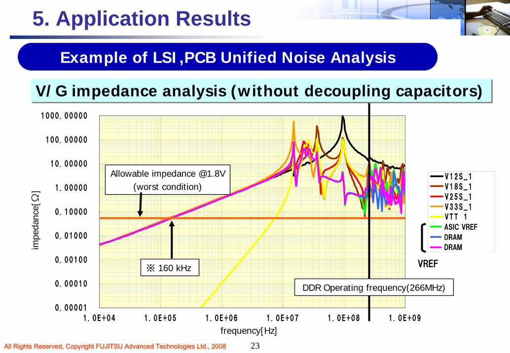
周波数解析(インピーダンス)
0.00001
0.00010
0.00100
0.01000
0.10000
1.00000
10.00000
100.00000
1000.00000
1.0E+04 1.0E+05 1.0E+06 1.0E+07 1.0E+08 1.0E+09
周波数 (Hz)
インピーダンス (Ω) V12S_1
V18S_1
V25S_1
V33S_1
VTT_1
DENEB_AA22
DIMM_1
DRAM4_49
Allowable impedance @1.8V(worst condition)
DDR Operating frequency(266MHz)
※ 160 kHz VREF
ASIC VREF
DRAM
DRAM
V/G impedance analysis (without decoupling capacitors)V/G impedance analysis (without decoupling capacitors)
frequency[Hz]
impe
danc
e[Ω
]5. Application Results
Example of LSI,PCB Unified Noise Analysis
23

All Rights Reserved, Copyright FUJITSU Advanced Technologies Ltd., 2008
周波数解析(インピーダンス)
0.00001
0.00010
0.00100
0.01000
0.10000
1.00000
10.00000
100.00000
1000.00000
1.0E+04 1.0E+05 1.0E+06 1.0E+07 1.0E+08 1.0E+09
周波数 (Hz)
イン
ピー
ダン
ス (Ω
) V12S_1
V18S_1
V25S_1
V33S_1
VTT_1
DENEB_AA22
DIMM_1
DRAM4_49
Allowable impedance @1.8V(worst condition)
VREF
ASIC VREF
DRAM
DRAM
Suppress impedanceunder
allowable impedance
frequency[Hz]
impe
danc
e[Ω
]
DDR Operating frequency(266MHz)
V/G impedance analysis (with decoupling capacitors)V/G impedance analysis (with decoupling capacitors)
5. Application Results
Example of LSI,PCB Unified Noise Analysis
24

All Rights Reserved, Copyright FUJITSU Advanced Technologies Ltd., 2008
VDE2
VIH
VIL
VTT
ASIC output pinDRAM input pin
■ : without V/G noise■ : with V/G noise
Delay variation iswithin allowable value
Verification of DDR data delay variation caused by V/G noise
5. Application Results
Example of LSI,PCB Unified Noise Analysis
25

All Rights Reserved, Copyright FUJITSU Advanced Technologies Ltd., 2008 26
6. Conclusion
■ Fujitsu’s LSI,PCB Unified Noise Analysis System wereintroduced and the effectiveness of the system were explained.
■ Further developments of the noise countermeasure design system to overcome the rapid advances oftechnology are scheduled.

All Rights Reserved, Copyright FUJITSU Advanced Technologies Ltd., 2008 27
7. Future Tasks
■ The LSI,PCB Unified Noise Analysis Technology has beenestablished as explained today. But,it is difficult to obtain the various LSI models available for power noise analysis(DDR,FPGA,ASIC,ASSP ・・・).
■ Sufficient supply of LSI power noise models are required.
■ It is one of the most desirable solutions for this problem that the standard IBIS models available for power noiseanalysis are widely supplied by LSI vendors.
■ We hope IBIS Forum and JEITA will promote to establishthe standard IBIS model for power noise analysis and spread it widely as a future task.

All Rights Reserved, Copyright FUJITSU Advanced Technologies Ltd., 2008 28