Embed Size (px)
Citation preview
NOISE ANALYSIS IN CMOS IMAGE SENSORS
a dissertation
submitted to the department of applied physics
and the committee on graduate studies
of stanford university
in partial fulfillment of the requirements
for the degree of
doctor of philosophy
By
Hui Tian
August 2000
c Copyright 2000 by Hui Tian
All Rights Reserved
ii
I certify that I have read this dissertation and that in my
opinion it is fully adequate, in scope and in quality, as a
dissertation for the degree of Doctor of Philosophy.
Abbas El Gamal(Principal Adviser)
I certify that I have read this dissertation and that in my
opinion it is fully adequate, in scope and in quality, as a
dissertation for the degree of Doctor of Philosophy.
Calvin F. Quate
I certify that I have read this dissertation and that in my
opinion it is fully adequate, in scope and in quality, as a
dissertation for the degree of Doctor of Philosophy.
R. Fabian Pease
Approved for the University Committee on Graduate
Studies:
iii
Abstract
Digital cameras are rapidly becoming the dominant image capture devices. They are
not only replacing �lm cameras, but also enabling many new applications. Among
the most important trends in digital camera design is the use of CMOS image sensors
instead of Charge-coupled devices (CCDs). Using CMOS technology enables the
integration of capture and processing on a single chip, which reduces system power
and cost. CMOS image sensors, however, have lower performance than CCDs mainly
due to higher temporal noise and nonuniformity.
Temporal noise sets the fundamental limit on image sensor performance under
low illumination and in video applications. In a CCD image sensor, noise is primarily
due to the photodetector shot noise and the output ampli�er thermal and 1/f noise.
CMOS image sensors su�er from higher noise than CCDs due to the additional pixel
and column ampli�er transistor thermal and 1/f noise, and noise analysis is further
complicated by the nonstationarity of the circuit models and the 1/f noise, and the
nonlinearity of the charge to voltage conversion.
The thesis presents the �rst complete and rigorous analysis of temporal noise in
CMOS image sensors that takes into consideration these complicating factors. Us-
ing time domain analysis, instead of the more traditional frequency domain analysis
method, we �nd that the reset noise power due to thermal noise is at most half of
its commonly quoted KTC value. This fundamental result is corroborated by sever-
al published experimental data including data collected in our lab. The lower reset
noise, however, comes at the expense of image lag. We �nd that alternative reset
methods such as overdriving the reset transistor gate or using a pMOS transistor can
alleviate lag, but double the reset noise power. We propose a new reset method that
iv
alleviates lag without increasing reset noise. To analyze the e�ect of 1/f noise on
CMOS image sensors we introduce a nonstationary extension of the recently devel-
oped, and generally agreed upon physical model for 1/f noise in MOS transistors. We
show that this nonstationary model can be used to obtain accurate estimates of the
e�ect of 1/f noise in switched circuits such as ring oscillators. Using our model and
time domain analysis, we �nd that the conventional frequency domain analysis results
using the stationary noise model can be very inaccurate, especially in estimating the
1/f noise e�ect of the reset transistor.
v
Acknowledgments
I would like to �rst and foremost thank my advisor Professor Abbas El Gamal for
his invaluable guidance and support, and for encouraging me to perform this thesis
work. His insightful and witty comments have made my PhD life very enjoyable. I
am grateful to Professor Calvin Quate for being my associate advisor, and for serving
on my oral and reading committee. I would like to thank Professor Fabian Pease for
serving on my oral and reading committee, and for the helpful discussion that partially
led to my work on 1/f noise. I would also like to thank Professor Brian Wandell for
chairing my oral committee, and for the enlightening and enjoyable discussions.
From the �rst day of my PhD research, Dr. Boyd Fowler stands out in helping
me intellectually and socially. I thank him for his guidance and help. I also wish
to thank Dr. Michael Godfrey for computer and lab support, and for the interesting
conversations. Dr. Hao Min also helped me a lot in the image sensor lab and I thank
him. I have worked with Dr. David Yang for years, and thank him for the enjoyable
cooperation.
My time at Stanford has been intellectually and socially enriched by the friends I
have made. I thank all my oÆcemates, T. Chen, S. H. Lim, X. Liu, and K. Salama,
for all the helpful discussion and comments, and for the fun activities in and out of the
oÆce. I would also like to thank P. Catrysse, J. DiCarlo, R. Erdmann, S. Kleinfelder,
and F. Xiao, for the helps and the helpful discussions. I am in debt to L. Lindgren
and W. Yu for their great helps.
I wish to thank Professor Geballe for supporting me in the �rst quarter I came
to Stanford. I thank Professor Shen for being my academic advisor during my �rst
two years of PhD study. I appreciate Professor Gill for his help with computer
vi
administration. I thank Charlotte Coe for the help throughout my stay in the research
group. I also thank Paula Perron for the administrative work and help.
I would like to thank Analog Devices Inc. and Urbanek family, for supporting me
through fellowship. I also thank Agilent, Canon, HP, Interval Research, and Kodak
for funding the PDC project, and for supporting me.
Finally and de�nitely not the lest, I would like to thank my parents, my sister,
and my wife for their love and support. I dedicate this thesis to them.
vii
Contents
Abstract iv
Acknowledgments vi
1 Introduction 1
1.1 CCD and CMOS Image Sensors . . . . . . . . . . . . . . . . . . . . . 1
1.2 Noise in CMOS Image Sensors . . . . . . . . . . . . . . . . . . . . . . 4
1.3 Thesis Organization . . . . . . . . . . . . . . . . . . . . . . . . . . . . 7
2 Temporal Noise in CMOS Image Sensors 9
2.1 Introduction . . . . . . . . . . . . . . . . . . . . . . . . . . . . . . . . 9
2.2 Mathematical Background . . . . . . . . . . . . . . . . . . . . . . . . 10
2.3 Noise in Integrated Circuits . . . . . . . . . . . . . . . . . . . . . . . 16
2.3.1 Fundamental Noise Sources . . . . . . . . . . . . . . . . . . . 16
2.3.2 Noise Models for Photodiode and MOSFET . . . . . . . . . . 18
2.3.3 Analysis of noise in linear circuits . . . . . . . . . . . . . . . . 22
2.4 CMOS Photodiode Active Pixel Sensors . . . . . . . . . . . . . . . . 26
2.5 Summary . . . . . . . . . . . . . . . . . . . . . . . . . . . . . . . . . 30
3 Analysis of Thermal and Shot Noise in CMOS APS 31
3.1 Introduction . . . . . . . . . . . . . . . . . . . . . . . . . . . . . . . . 31
3.2 Noise Due to Reset . . . . . . . . . . . . . . . . . . . . . . . . . . . . 32
3.3 Image Lag Due to Incomplete Reset . . . . . . . . . . . . . . . . . . . 40
3.4 Noise Due to Integration . . . . . . . . . . . . . . . . . . . . . . . . . 44
viii
3.5 Noise Due to Readout . . . . . . . . . . . . . . . . . . . . . . . . . . 46
3.6 Summary . . . . . . . . . . . . . . . . . . . . . . . . . . . . . . . . . 50
4 Experiments 51
4.1 Introduction . . . . . . . . . . . . . . . . . . . . . . . . . . . . . . . . 51
4.2 Experiment Setup and Procedure . . . . . . . . . . . . . . . . . . . . 52
4.3 Experimental Results . . . . . . . . . . . . . . . . . . . . . . . . . . . 58
4.4 Summary . . . . . . . . . . . . . . . . . . . . . . . . . . . . . . . . . 61
5 MOSFET 1/f Noise Models 64
5.1 Introduction . . . . . . . . . . . . . . . . . . . . . . . . . . . . . . . . 64
5.2 Standard 1/f Noise Model . . . . . . . . . . . . . . . . . . . . . . . . 65
5.3 Nonstationary 1/f Noise Model . . . . . . . . . . . . . . . . . . . . . 69
5.4 1/f Noise in a Periodically Switched Transistor . . . . . . . . . . . . . 72
5.5 1/f-induced Phase Noise in a Ring Oscillator . . . . . . . . . . . . . . 76
5.6 Summary . . . . . . . . . . . . . . . . . . . . . . . . . . . . . . . . . 78
6 Analysis of 1/f Noise in CMOS APS 81
6.1 Introduction . . . . . . . . . . . . . . . . . . . . . . . . . . . . . . . . 81
6.2 1/f Noise Due to the Follower and Access Transistors . . . . . . . . . 82
6.3 1/f Noise Due to the Reset Transistor . . . . . . . . . . . . . . . . . . 85
6.4 Summary . . . . . . . . . . . . . . . . . . . . . . . . . . . . . . . . . 89
7 Conclusion 91
7.1 Summary . . . . . . . . . . . . . . . . . . . . . . . . . . . . . . . . . 91
7.2 Future Work and Future Directions . . . . . . . . . . . . . . . . . . . 93
Bibliography 95
ix
List of Tables
4.1 64�64 CMOS APS Test Structure Characteristics. . . . . . . . . . . . 58
x
List of Figures
1.1 Digital camera system. . . . . . . . . . . . . . . . . . . . . . . . . . . 2
1.2 Block diagram of a typical interline transfer CCD image sensors. . . . 2
1.3 Block diagram of a typical CMOS image sensors. . . . . . . . . . . . 4
2.1 Probability density function of a Gaussian random variable. . . . . . 12
2.2 Power spectral density of a band-limited white noise process. . . . . . 14
2.3 Autocorrelation function of a band-limited white noise process. . . . . 14
2.4 Waveform of a band-limited white noise process. . . . . . . . . . . . . 15
2.5 Noise model of a thermal noise source. . . . . . . . . . . . . . . . . . 17
2.6 Noise model of a shot noise source. . . . . . . . . . . . . . . . . . . . 18
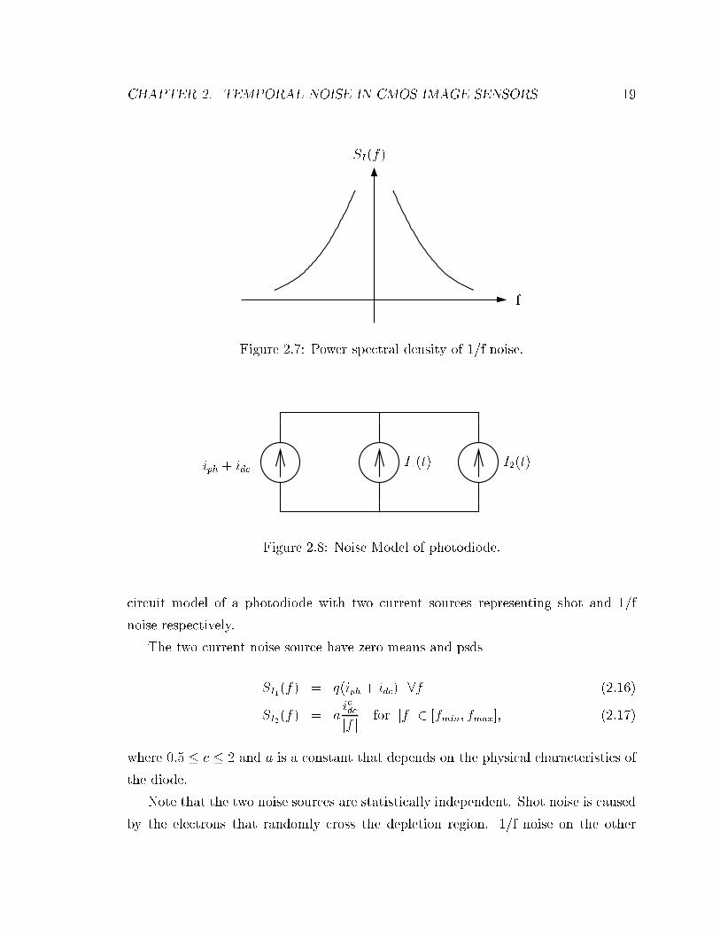
2.7 Power spectral density of 1/f noise. . . . . . . . . . . . . . . . . . . . 19
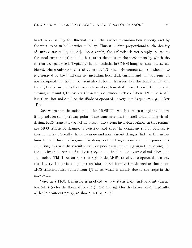
2.8 Noise Model of photodiode. . . . . . . . . . . . . . . . . . . . . . . . 19
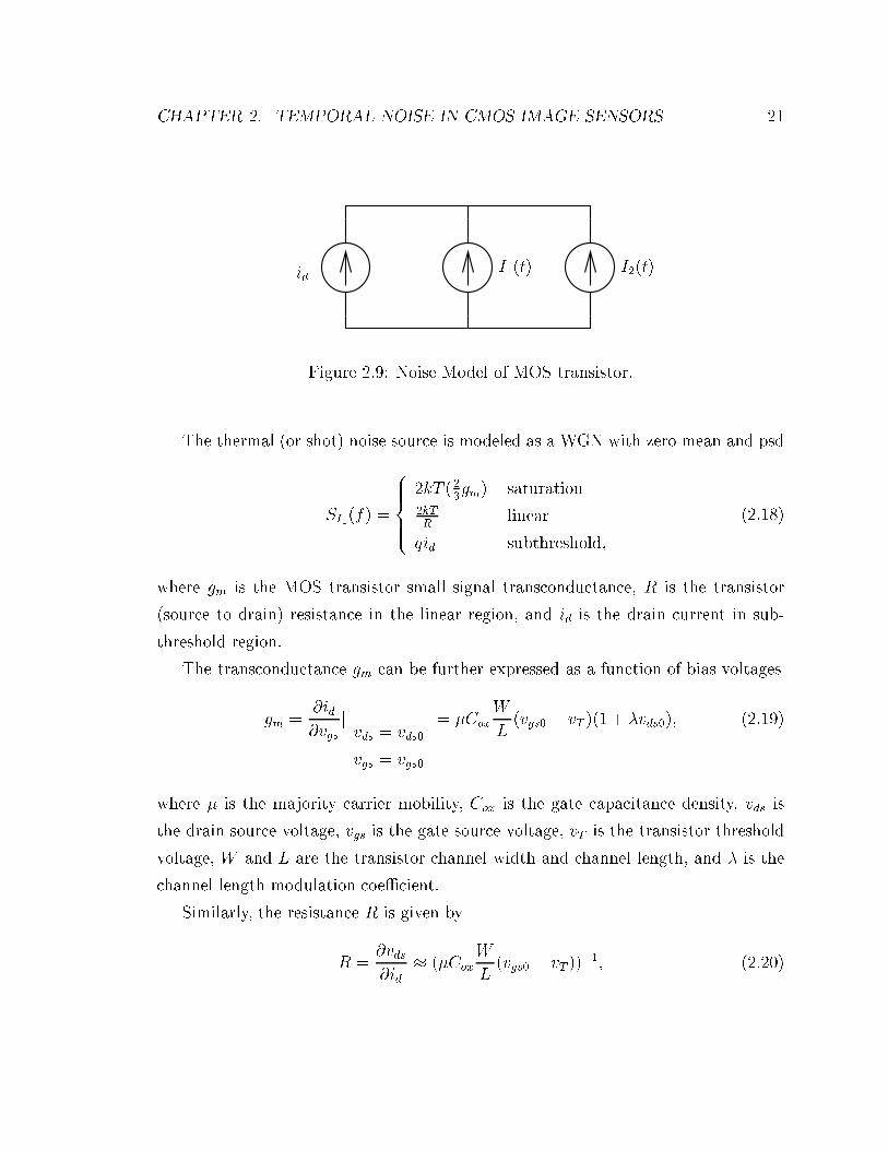
2.9 Noise Model of MOS transistor. . . . . . . . . . . . . . . . . . . . . . 21
2.10 Integrator circuit. . . . . . . . . . . . . . . . . . . . . . . . . . . . . . 23
2.11 Linear time invariant circuit. . . . . . . . . . . . . . . . . . . . . . . . 24
2.12 RC circuit. . . . . . . . . . . . . . . . . . . . . . . . . . . . . . . . . . 25
2.13 A linear time invariant circuit with multiple noise sources. . . . . . . 26
2.14 CMOS photodiode APS circuit and timing diagram. . . . . . . . . . . 28
2.15 Noise sources in CMOS APS pixel level circuit. . . . . . . . . . . . . 29
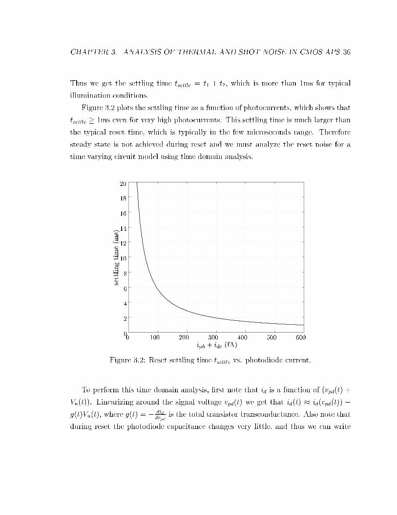
3.1 CMOS APS circuit noise model during reset. . . . . . . . . . . . . . . 33
3.2 Reset settling time tsettle vs. photodiode current. . . . . . . . . . . . . 36
3.3 Simulated photodiode voltage waveform due to incomplete reset. r1
and r2 refer to the end of reset for the �rst and second frames respectively. 41
xi
3.4 pMOS (left) and overdriving gate (right) reset methods. . . . . . . . . 42
3.5 Pseudo- ash reset method. . . . . . . . . . . . . . . . . . . . . . . . . 43
3.6 Signal voltage vs. photodiode current. . . . . . . . . . . . . . . . . . 46
3.7 RMS noise voltage vs. photodiode current. . . . . . . . . . . . . . . . 47
3.8 CMOS APS circuit noise model during readout. . . . . . . . . . . . . 48
3.9 Readout noise power spectral density due to M2, M3, and M4. . . . . 49
4.1 Experiment setup for CMOS image sensors characterization. . . . . . 54
4.2 CMOS APS output waveform . . . . . . . . . . . . . . . . . . . . . . 59
4.3 CMOS APS output mean as a function of time for segments 1, 2, and 3. 59
4.4 CMOS APS output variance as a function of time for segments 1, 2,
and 3. . . . . . . . . . . . . . . . . . . . . . . . . . . . . . . . . . . . 60
4.5 Simulated vs. measured signal to noise ratio. . . . . . . . . . . . . . . 62
4.6 Measured �nal reset voltage for �ve consecutive frames (indicated by � ) ,
and the simulated photodiode voltage waveform (indicated by the dashed
lines). . . . . . . . . . . . . . . . . . . . . . . . . . . . . . . . . . . . 62
5.1 MOSFET with single trap in its gate oxide (top) and the resulting
trapped electron number N(t) waveform (bottom). . . . . . . . . . . 67
5.2 1/f noise psd as the summation of psds due to multiple traps. . . . . 68
5.3 Energy-band diagram for MOSFET, with an active trap inside its gate
oxide. Solid lines are used when the transistor is o�, and dashed lines
are used when the transistor is on. . . . . . . . . . . . . . . . . . . . 70
5.4 RMS gate voltage of an nMOS transistor with 1�m2 channel area (top)
and the percentage error using the standard model (bottom). . . . . . 73
5.5 Spectrum analysis of a periodically switched nMOS transistor. . . . . 75
5.6 Simulated 1/f noise psd for switched and dc biased transistors. . . . . 76
5.7 The gate voltage of the dominant nMOS transistor in a ring oscillator
(top), the associated ISF (middle), and �(t) for � = 31:6kHz (bottom). 79
5.8 Simulated 1/f-induced phase noise psd for a ring oscillator. . . . . . . 80
6.1 Small signal model for 1/f noise analysis during readout. . . . . . . . 83
xii
6.2 Bitline RMS 1/f noise voltage due to the follower transistor. . . . . . 86
6.3 Bitline RMS 1/f noise voltage due to the access transistor. . . . . . . 86
6.4 CMOS APS circuit during reset (a), and the corresponding small signal
model for 1/f noise analysis (b). . . . . . . . . . . . . . . . . . . . . . 87
6.5 Simulated output referred RMS 1/f reset noise using frequency domain
analysis versus using the nonstationary extension and time domain
analysis. . . . . . . . . . . . . . . . . . . . . . . . . . . . . . . . . . . 89
6.6 Simulated output referred RMS 1/f reset noise using standard 1/f noise
model versus using the nonstationary extension, both assuming time
varying circuit model. . . . . . . . . . . . . . . . . . . . . . . . . . . . 90
xiii
Chapter 1
Introduction
1.1 CCD and CMOS Image Sensors
As more and more people have gained access to the rapidly expanding internet and the
ever increasing personal computing power, digital cameras are becoming very popular.
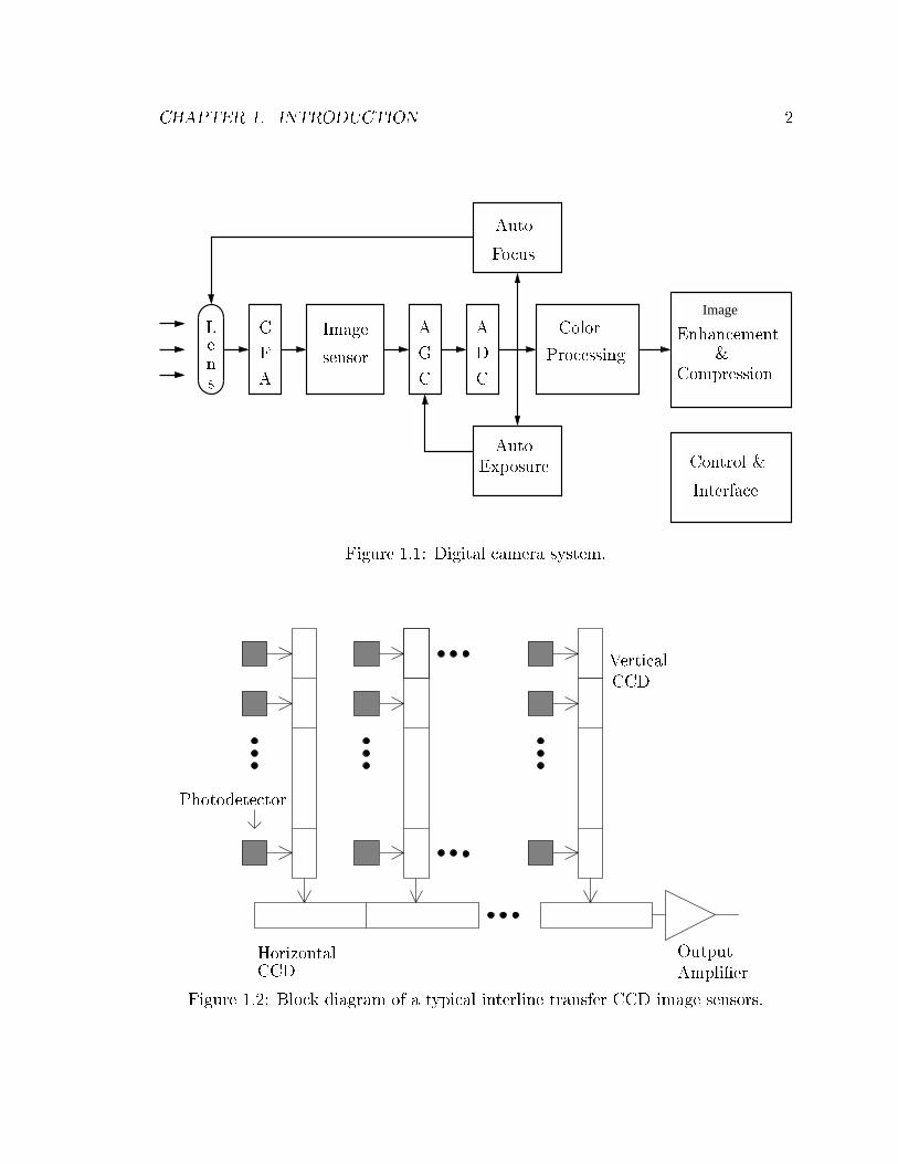
Figure 1.1 plots the block diagram of a typical digital camera system. The camera
can capture the optical scene and convert it directly into digital format. All the
traditional imaging pipeline functions, such as color processing, image enhancement
and image compression, can also be integrated into the camera. This enables the
quick processing and exchange of images. In addition, they can be made with small
size, light weight, low cost, and low power. As a result, digital cameras are quickly
replacing traditional �lm cameras. The unique features of digital cameras also enable
many new applications, such as network teleconferencing, video phones, guidance and
navigation, automotive applications, and robotic and machine vision, etc.
Most of the digital cameras today use the charge-coupled devices (CCDs) to im-
plement the image sensors. Figure 1.2 depicts the block diagram of the widely used
interline transfer CCD image sensors. In the CCD image sensors, incident photons
are converted to charge and then accumulated by the photodetectors during expo-
sure time. During the following readout time the accumulated charge is sequentially
transferred into the vertical and horizontal CCDs, and �nally shifted to the chip level
output ampli�er, where it is converted to voltage signal.
1
CHAPTER 1. INTRODUCTION 2
Image
Processing
Color
Auto
Auto
Focus
Exposure
Image
sensor
Enhancement
Compression
Control &
&
Interface
A
AA
G
C
CC
F D
Lens
Figure 1.1: Digital camera system.
Photodetector
Vertical
CCD
CCD
Output
Ampli�erHorizontal
Figure 1.2: Block diagram of a typical interline transfer CCD image sensors.
CHAPTER 1. INTRODUCTION 3
As the currently dominant image sensor technology used by digital cameras, CCD
image sensors can achieve superior noise performance and uniformity, with high �ll
factor, small pixel size, and large formats. Some limited signal processing operations
have also been demonstrated using CCD. The reason that CCD image sensors have
low noise and high uniformity is that the charge from every pixel is sequentially
converted to voltage signal by the same chip level output ampli�er.
However, this sequential readout of pixel charge limits the readout speed. Even
worse, because CCDs are high capacitance devices and all the CCDs are switched
at the same time with high voltages during readout, CCD image sensors usually
consume lots of power. Furthermore, since CCDs cannot be easily integrated with
CMOS circuits due to additional fabrication complexity and increased cost, it is very
hard to integrate all the camera functions onto a single CCD chip. Instead, multiple
chips have to be used. So normally CCD image sensors based digital cameras are
relatively large in size and consume high power, and thus are not well suited for
portable and embedded imaging applications.
To build portable and embedded imaging systems, it is critical to have the ca-
pability of integrating the image sensor together with the circuitry that drives the
image sensor and performs on chip signal conversion and processing. This high level
of integration not only enables small size of the imaging systems, but also reduces
the power consumption and simpli�es the system interface. Since Complementary
Metal-Oxide-Silicon (CMOS) technology is well suited for implementing on chip sig-
nal processing circuits, people start looking at using CMOS technology to implement
the image sensors. This leads to one of the most important trends in digital camera
design, which is the use of CMOS image sensors instead of CCDs as the imaging
devices.
Figure 1.3 plots the block diagram of a typical CMOS image sensors. Unlike
CCD image sensors, it adopts a digital memory style readout, using the row decoders
and column ampli�ers. By doing so, it overcomes many of the problems that CCD
image sensors have. Readout now can be very fast and consumes very low power.
Random access of pixel values becomes possible, allowing selective readout of windows
of interest. Analog signal processing can be integrated onto the same substrate, as
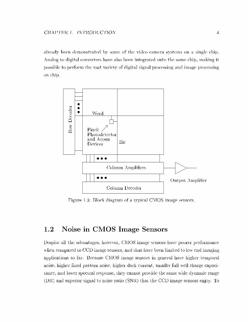
CHAPTER 1. INTRODUCTION 4
already been demonstrated by some of the video camera systems on a single chip.
Analog to digital converters have also been integrated onto the same chip, making it
possible to perform the vast variety of digital signal processing and image processing
on chip.
Word
RowDecoder
Pixel:Photodetectorand AccessDevices Bit
Column Ampli�ers
Column Decoder
Output Ampli�er
Figure 1.3: Block diagram of a typical CMOS image sensors.
1.2 Noise in CMOS Image Sensors
Despite all the advantages, however, CMOS image sensors have poorer performance
when compared to CCD image sensors, and thus have been limited to low end imaging
applications so far. Because CMOS image sensors in general have higher temporal
noise, higher �xed pattern noise, higher dark current, smaller full well charge capaci-
tance, and lower spectral response, they cannot provide the same wide dynamic range
(DR) and superior signal to noise ratio (SNR) that the CCD image sensors enjoy. To
CHAPTER 1. INTRODUCTION 5
see why this is the case, we brie y go over the history of CMOS image sensors here. A
detailed review of CMOS image sensors, including their ancestor MOS image sensors,
can be found in [10, 11] by Fossum.
Although MOS image sensors �rst appeared in the late 1960s [55], most of today's
CMOS image sensors are based on the study around the early 1980's. During that
time passive pixel sensor (PPS) was the CMOS image sensor technology of choice [8,
9, 39, 37, 38], which contains a photodetector and a single pass transistor within each
pixel. Charge sensing is used to readout the signals.
In the early 1990s active pixel sensor (APS) [10, 33, 32] becomes popular. In
contrast to the PPS approach that uses a simple switch to connect the pixel signal
charge to the column bus capacitance, APS adds some more active transistors to each
pixel. The in pixel active transistors can provide both gain and bu�ering functions,
and thus achieve lower noise readout, improved scalability to large array formats,
and higher speed readout, compared to PPS. With the advent of deep submicron
CMOS technologies and microlenses, APS has now become the CMOS image sensor
technology of choice [30, 46, 36].
Most recently digital pixel sensor (DPS) [13, 58, 60] emerges. Unlike APS and
PPS, where the analog to digital (A/D) conversion is performed at chip level or
column level, DPS integrates an A/D converter into each pixel. By performing the
A/D conversion in parallel for all pixels, the DPS holds the promise of even faster
operation, lower power, and higher SNR, when compared with APS.
Because each pixel contains one or more transistors, �xed pattern noise (FPN)
had been the primary concern for CMOS image sensors. This was also one of the
major reasons that helped CCD image sensors to become the dominant solid state
imaging technology. Fortunately the development of both on chip signal processing,
mainly the correlated double sampling (CDS) technique, and o� chip digital signal
processing (DSP) have helped to reduce the FPN to acceptable range.
However, temporal noise performance of CMOS image sensors still lag behind
CCD image sensors. Since it sets the fundamental limit in sensor dynamic range,
and reduces the sensor signal to noise ratio especially under low light conditions, high
end imaging applications usually have abandoned CMOS sensors so far. Thus a fully
CHAPTER 1. INTRODUCTION 6
understanding of noise mechanism in CMOS image sensors becomes necessary, and
is essential to guide the development of the next generation of CMOS image sensors.
In a CCD image sensor, temporal noise is well studied and characterized. It
is primarily due to the photodetector shot noise and the output ampli�er thermal
and 1/f noise. CMOS image sensors su�er from higher noise than CCDs due to the
additional pixel and column ampli�er transistor thermal and 1/f noise, and noise
analysis is further complicated by the nonstationarity of the circuit models and the
nonstationary noise sources including 1/f noise, and the nonlinearity of the charge to
voltage conversion.
There have been extensive study on noise in CMOS image sensors. During the
whole procedure of design, fabrication, and characterization of CMOS image sensors,
noise is always one of the most important parameters to be considered. This previous
study helps us tremendously in understanding the noise problem in CMOS image sen-
sors. However, in previous work it is often assumed that the circuit is time invariant,
and that the noise sources are stationary. Stationary noise of a time invariant circuit
can be readily analyzed in the frequency domain using spectral density functions.
In real image sensors the situation is quite di�erent. The voltages, currents,
conductances, and capacitances of the sensor circuitry are often changing rapidly. As
a result, the noise is not stationary and the circuit is not time invariant. Under such
conditions, the conventional frequency domain analysis often fails to generate results
that are consistent with experiments.
Since MOSFETs are used inside each pixel, CMOS image sensors exhibit higher
1/f noise compared with CCD. This type of noise is particularly annoying to ob-
servers because of the low pass �ltering characteristics of human eyes. The common
technique for reducing 1/f noise is to increase the gate area of the transistor. How-
ever, in CMOS image sensors one must conserve as much chip area as possible for
the photodetector. Even if the size can be increased, the use of a large area leads
to an excessive input capacitance, which can adversely a�ect the charge conversion
eÆciency and bandwidth. The analysis of 1/f noise in a time varying circuit, again,
is not well established.
In this thesis, we present the �rst complete and rigorous analysis of temporal noise
CHAPTER 1. INTRODUCTION 7
in CMOS image sensors that takes into consideration these complicating factors. We
focus on developing the methodology and models. Since APS is the technology of
choice for now and it well demonstrates the methods to analyze noise in CMOS image
sensors, we will use it as the example sensor throughout this thesis. The methodology
and models we developed here can be easily applied to analyze temporal noise in other
image sensors, including both PPS and DPS.
1.3 Thesis Organization
Chapter 2 introduces the backgrounds for analyzing noise in CMOS image sensors.
We �rst review the mathematical background for noise analysis, including random
variables and random processes. We then go over the noise models of basic integrated
circuit components, and introduce the superposition principle of �nding the total
output noise power for a linear circuit. We also describe the circuit, operation, and
noise sources of CMOS photodiode APS, which we will use as an example throughout
the thesis.
Chapter 3 presents a detailed and rigorous analysis of noise due to thermal and
shot noise sources in photodiode APS. We show that during reset the conventional
frequency domain noise analysis method cannot be applied. To calculate reset noise
power we consider the time varying reset circuit model and perform time-domain
noise analysis using the MOS transistor subthreshold noise model. We �nd that reset
noise power is at most half of its commonly quoted kT
Cvalue, which corroborates the
published experimental results. The lower reset noise, however, comes at the expense
of image lag. We propose a new \pseudo- ash" reset method, which can alleviate
image lag without increasing reset noise. We then present an analysis of photodiode
shot noise that takes into consideration the nonlinearity of the photodiode charge to
voltage conversion.
Chapter 4 describes the setup and methods we use to characterize CMOS APS.
Using them we measure the capacitance, conversion gain, quantum eÆciency, pattern
noise, and temporal noise for the test structures fabricated in 0.35� CMOS process-
es. We �nd that the measured reset noise mean square value is indeed close to kT
2C.
CHAPTER 1. INTRODUCTION 8
The measured SNR curve also matches well with our analysis. We demonstrate the
incomplete reset induced image lag.
Chapter 5 proposes a nonstationary extension of the standard 1/f noise model,
which accurately models 1/f noise when the transistor is switched from the o� to the
on state. We apply our nonstationary model to estimate the e�ect of 1/f noise on a
periodically switched transistor, and a ring oscillator, respectively. In both cases we
�nd that our estimates are consistent with the reported measurement results.
Chapter 6 presents the analysis of 1/f noise in CMOS APS. We analyze the 1/f
noise due to the pixel level transistors using time domain analysis and our nonsta-
tionary 1/f noise model. We show that the conventional frequency domain analysis,
which requires an arbitrarily de�ned low cuto� frequency, can produce very inaccurate
estimates of 1/f noise power.
Finally chapter 7 concludes the thesis and discusses the most likely directions for
future related research.
Chapter 2
Temporal Noise in CMOS Image
Sensors
2.1 Introduction
Temporal noise is the temporal variation in pixel output values under constant illumi-
nation. Usually temporal noise in image sensors increases when the illumination gets
stronger. At the same time the signal also increases, with a even faster speed. As a
result the signal to noise ratio (SNR) usually improves as the illumination increases.
Since it is SNR, instead of noise, that directly a�ects the image quality, the noise
e�ect is most pronounced at low illumination levels. Noise also sets a fundamental
limit on image sensor dynamic range (DR), which is another very important image
quality metric.
There are many sources that can cause temporal noise in CMOS image sensors.
Shot noise occurs when photo-electrons are generated and when dark current electrons
are presented. Additional noise is added when resetting the photodetector (reset
noise) and when reading out the pixel value (readout noise). If the output analog
signal is to be digitized, then quantization noise must also be included. Power supply
uctuation can be coupled to the image sensor array and thus cause noise. Noise can
also be injected to the sensor from peripheral circuits through substrate coupling.
The environmental interferences such as temperature variation, light source humming,
9
CHAPTER 2. TEMPORAL NOISE IN CMOS IMAGE SENSORS 10
electromagnetic �eld, etc., can cause the uctuation in the sensor output, and thus
cause the temporal noise.
Some of the noise can be minimized by good circuit design practice. For example,
substrate noise can be reduced by carefully implementing guard rings or by changing
the layout. The power supply noise can be reduced by increasing the readout circuit
power supply rejection ratio, or by simply using a cleaner power supply. Environmen-
tal interferences can be reduced by shielding, cabling, grounding, or by rearranging
the whole setup. In the thesis, we are mainly concerned with the intrinsic noise that
is generated internally by the CMOS image sensors. The intrinsic noise usually is
hard to suppress, and is resulted from the physics of the integrated circuit devices.
It includes three major types of noise, namely thermal noise, shot noise, and icker
noise.
In this chapter we go over some of the math and circuit background that is needed
to analyze noise in CMOS image sensors. Then we describe the circuit and operation
of CMOS active pixel sensors (APS), which we will be using as an example throughout
the thesis.
The rest of the chapter is organized as follows. In section 2.2, we introduce the
mathematical background for noise analysis, including random variables and random
processes. In section 2.3 we describe the noise models of the basic integrated circuit
components, and introduce the superposition principle of �nding the total output
noise power for a linear circuit. In section 2.4, we describe the circuit and operation
of CMOS Active Pixel Sensors (APS). We then summarize the noise sources in CMOS
APS.
2.2 Mathematical Background
Noise phenomena normally have the property that we do not specify precisely what
magnitudes are observed at what time, either because we do not have the complete
knowledge or because the precise description is not necessary. For this reason noise
samples are conventionally modeled as continuously valued random variables, and
noise waveforms are modeled as random processes. A continuous valued random
CHAPTER 2. TEMPORAL NOISE IN CMOS IMAGE SENSORS 11
variable X is completely speci�ed by its probability density function (pdf)
fX(x) � 0;
Z1
�1
fX(x)dx = 1: (2.1)
From pdf one can calculate all the moments of the random variable. Among them
the most important two for noise analysis are the mean
X =
Z1
�1
xf(x)dx;
and the mean square
X2 =
Z1
�1
x2f(x)dx:
Mean square is often interpreted as the average power of a signal X. Square root
of this power (denoted as RMS) represents a equivalent constant signal with constant
power equaling to the average power of X. From the mean and mean square, we can
calculate the variance of X
�2X= X2 � (X)2;
which is interpreted as the square distance of X from its mean. When X has zero
mean, its variance is equal to the mean square. Variance is often used to estimate
the noise power.
The most often used random variable in noise analysis is Gaussian random vari-
able. It is used to describe the magnitude distribution of a large variety of noise
sources, including thermal, shot, and 1/f noise. Gaussian random variable has the
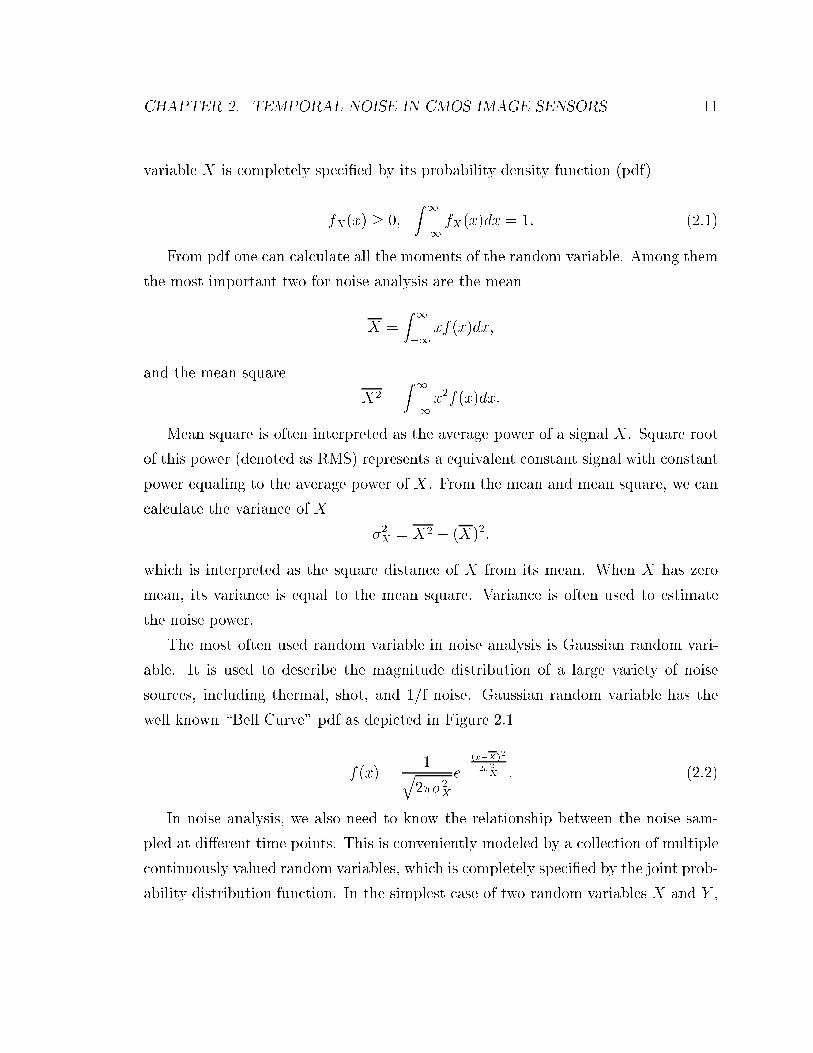
well known \Bell Curve" pdf as depicted in Figure 2.1
f(x) =1q2��2
X
e�
(x�X)2
2�2X : (2.2)
In noise analysis, we also need to know the relationship between the noise sam-
pled at di�erent time points. This is conveniently modeled by a collection of multiple
continuously valued random variables, which is completely speci�ed by the joint prob-
ability distribution function. In the simplest case of two random variables X and Y ,
CHAPTER 2. TEMPORAL NOISE IN CMOS IMAGE SENSORS 12
X
f(x)
x
Figure 2.1: Probability density function of a Gaussian random variable.
the joint pdf f(x,y) must satisfy that
f(x; y) � 0;
Z1
�1
Z1
�1
f(x; y)dxdy = 1: (2.3)
The relationship between these two random variables X and Y is then described
by the correlation function
XY =
Z1
�1
Z1
�1
xyf(x; y)dxdy: (2.4)
If XY = X � Y , then X and Y are uncorrelated. If f(x; y) = fX(x)fY (y) they
are independent of each other. It can be easily shown that two independent random
variables must be uncorrelated. The reverse statement does not hold in general,
although for jointly Gaussian random variables it is true.
A random process X(t), �1 � t � 1 is used to model the noise waveform.
It is an in�nite collection of random variables (noise samples) indexed by time t.
For any time instances t1; t2; : : : ; tn , the samples X(t1); X(t2); : : : ; X(tn) are random
variables. In noise analysis, it is often important to know the process mean X(t) and
autocorrelation function RX(t+ �; t) = X(t+ �)X(t).
Many important noise processes are modeled as stationary random processes, i.e.,
processes with time invariant statistics. If both mean and autocorrelation function
CHAPTER 2. TEMPORAL NOISE IN CMOS IMAGE SENSORS 13
are time invariant, i.e., X(t) = � and RX(t + �; t) = RX(�), then X(t) is a wide
sense stationary (WSS) process and its autocorrelation function has the following
properties
� RX(0) = X2(t), which has the interpretation of average process power.
� RX(�) is an even function.
� jRX(�)j � RX(0), for all � .
The power spectral density (psd) of a WSS process X(t) is the Fourier Transform
of RX(�)
SX(f) = F [RX(�)] =
Z1
�1
RX(�)e�j2�f�d�; �1 � f � 1 (2.5)
It can be shown that the psd must satisfy
� SX(f) � 0, and is an even function.
� P = X2(t) =R1
�1SX(f)df .
� P [f1; f2] = 2Rf2f1 SX(f)df ,
where P denotes average power, and P [f1; f2] denotes average power in frequency
band [f1; f2].
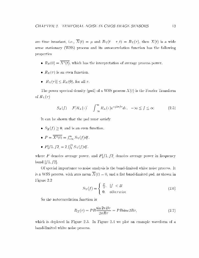
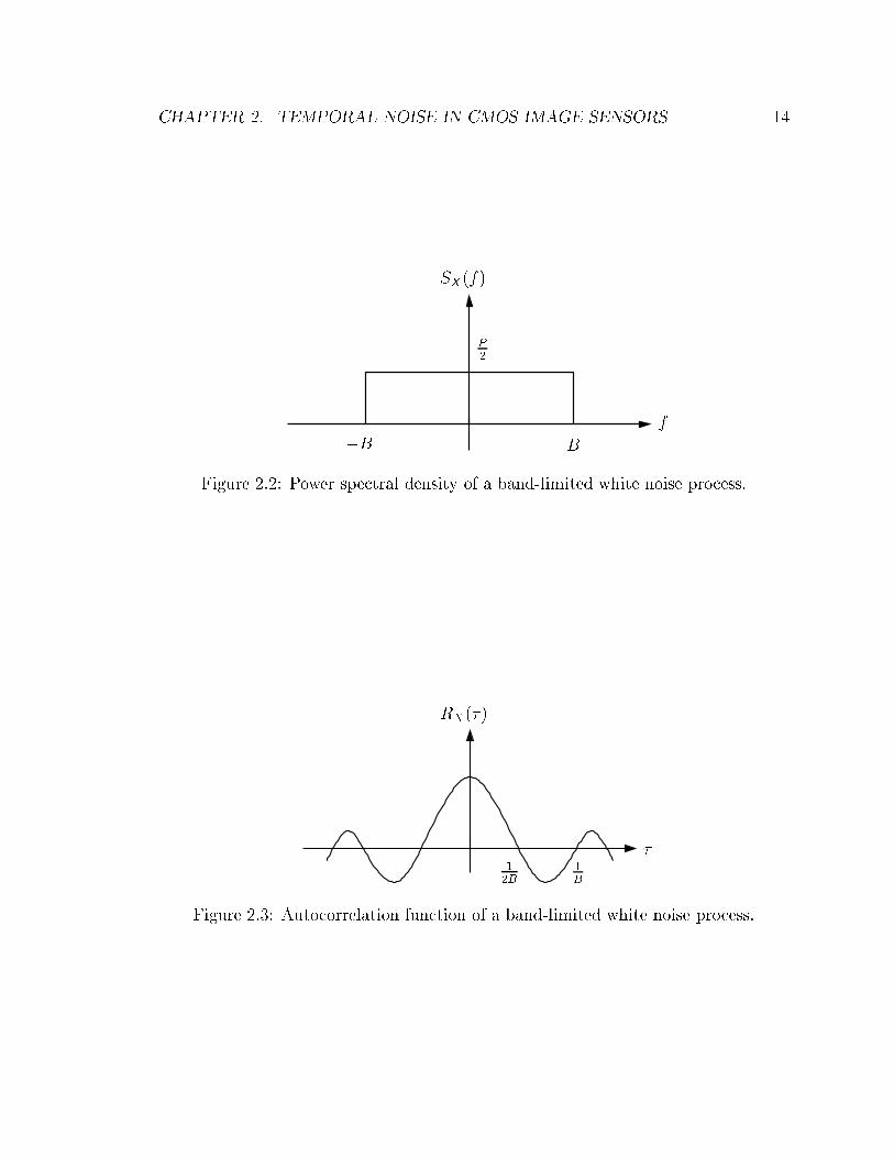
Of special importance to noise analysis is the band-limited white noise process. It
is a WSS process, with zero mean X(t) = 0, and a at band-limited psd, as shown in
Figure 2.2
SX(f) =
8<:
P
2; jf j < B
0; otherwise(2.6)
So the autocorrelation function is
RX(�) = PBsin 2�B�
2�B�= PBsinc2B�; (2.7)
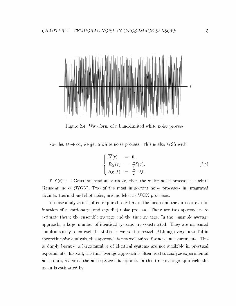
which is depicted in Figure 2.3. In Figure 2.4 we plot an example waveform of a
band-limited white noise process.
CHAPTER 2. TEMPORAL NOISE IN CMOS IMAGE SENSORS 14
f
B�B
P
2
SX(f)
Figure 2.2: Power spectral density of a band-limited white noise process.
�1B
12B
RX(�)
Figure 2.3: Autocorrelation function of a band-limited white noise process.
CHAPTER 2. TEMPORAL NOISE IN CMOS IMAGE SENSORS 15
t
Figure 2.4: Waveform of a band-limited white noise process.
Now let B !1, we get a white noise process. This is also WSS with
8>>><>>>:
X(t) = 0;
RX(�) = P
2Æ(�);
SX(f) = P
28f:
(2.8)
If X(t) is a Gaussian random variable, then the white noise process is a white
Gaussian noise (WGN). Two of the most important noise processes in integrated
circuits, thermal and shot noise, are modeled as WGN processes.
In noise analysis it is often required to estimate the mean and the autocorrelation
function of a stationary (and ergodic) noise process. There are two approaches to
estimate them: the ensemble average and the time average. In the ensemble average
approach, a large number of identical systems are constructed. They are measured
simultaneously to extract the statistics we are interested. Although very powerful in
theoretic noise analysis, this approach is not well suited for noise measurements. This
is simply because a large number of identical systems are not available in practical
experiments. Instead, the time average approach is often used to analyze experimental
noise data, as far as the noise process is ergodic. In this time average approach, the
mean is estimated by
CHAPTER 2. TEMPORAL NOISE IN CMOS IMAGE SENSORS 16
< X(t) >T=1
T
ZT
0X(T )dt; (2.9)
and the autocorrelation is estimated by
< RX(�) >T=1
T
ZT
0X(T )X(T + �)dt: (2.10)
Power spectral density is then found to be
SX(f) =1
n
nXi=1
F [< RX(�) >i
T]: (2.11)
Note here that the psd cannot be estimated using the periodogram
F [< RX(�) >T ]:
The estimator mentioned here estimates RX(�) n times and takes the average of the
periodograms.
2.3 Noise in Integrated Circuits
In this section we introduce the physical models that are often used to analyze the
noise in integrated circuits. We �rst describe the basic noise sources in integrated
circuits. Then in subsection 2.3.2 we summarize the noise models of the most often
used devices in CMOS image sensors, including the photodiode and the MOSFET.
In subsection 2.3.3 we show how the noise contributions from di�erent devices are
summed together, to get the total output (or input) referred noise power.
2.3.1 Fundamental Noise Sources
There are many sources that can cause noise in today's integrated circuits, such as
power supply uctuation, EM interference, substrate coupling, etc. Often times these
external interferences can be reduced to acceptable level, either by proper circuit
design practice, or by carefully applying shielding and grounding techniques. In this
CHAPTER 2. TEMPORAL NOISE IN CMOS IMAGE SENSORS 17
subsection we focus on the intrinsic noise that is hard to suppress, including thermal
noise, shot noise, and icker noise.
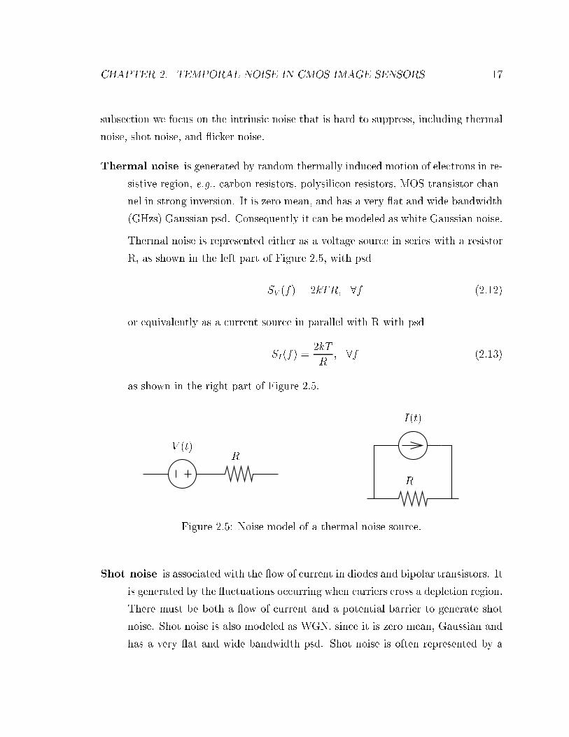
Thermal noise is generated by random thermally induced motion of electrons in re-
sistive region, e.g., carbon resistors, polysilicon resistors, MOS transistor chan-
nel in strong inversion. It is zero mean, and has a very at and wide bandwidth
(GHzs) Gaussian psd. Consequently it can be modeled as white Gaussian noise.
Thermal noise is represented either as a voltage source in series with a resistor
R, as shown in the left part of Figure 2.5, with psd
SV (f) = 2kTR; 8f (2.12)
or equivalently as a current source in parallel with R with psd
SI(f) =2kT
R; 8f (2.13)
as shown in the right part of Figure 2.5.
R
R
V (t)
I(t)
Figure 2.5: Noise model of a thermal noise source.
Shot noise is associated with the ow of current in diodes and bipolar transistors. It
is generated by the uctuations occurring when carriers cross a depletion region.
There must be both a ow of current and a potential barrier to generate shot
noise. Shot noise is also modeled as WGN, since it is zero mean, Gaussian and
has a very at and wide bandwidth psd. Shot noise is often represented by a
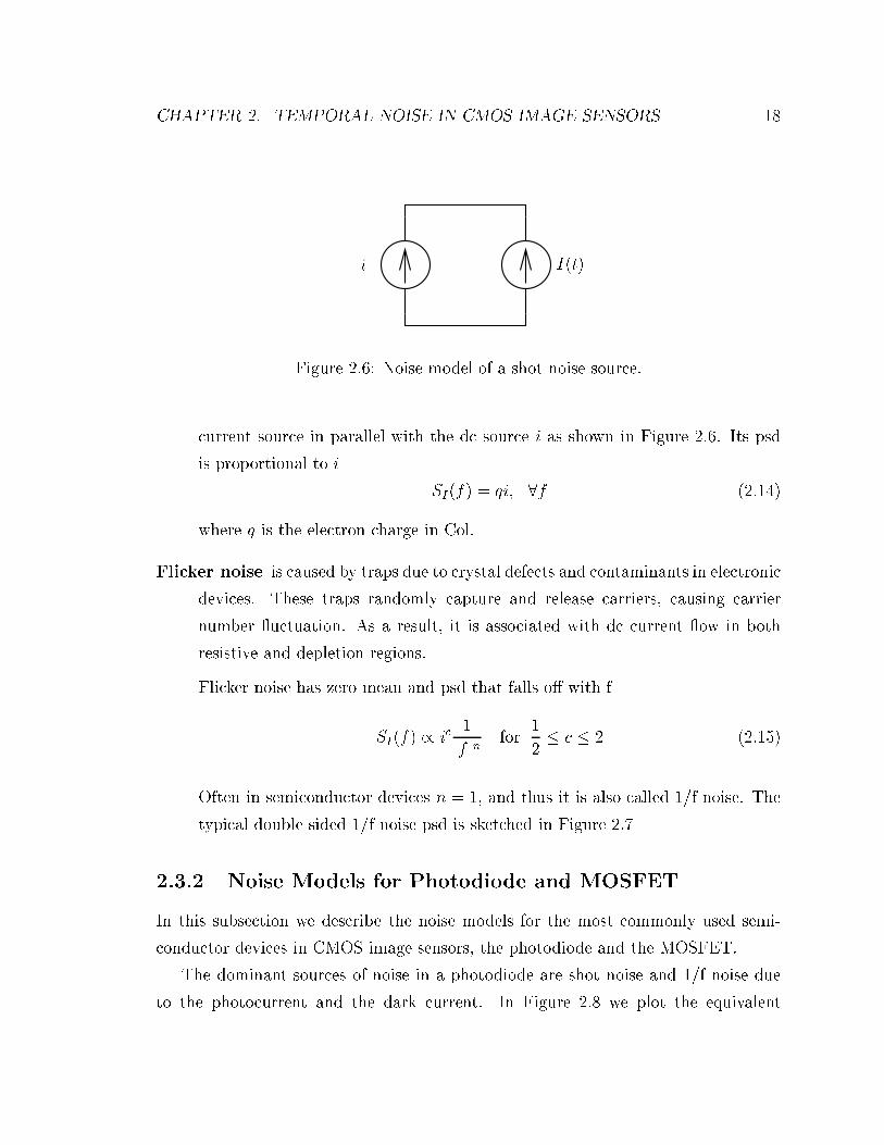
CHAPTER 2. TEMPORAL NOISE IN CMOS IMAGE SENSORS 18
i I(t)
Figure 2.6: Noise model of a shot noise source.
current source in parallel with the dc source i as shown in Figure 2.6. Its psd
is proportional to i
SI(f) = qi; 8f (2.14)
where q is the electron charge in Col.
Flicker noise is caused by traps due to crystal defects and contaminants in electronic
devices. These traps randomly capture and release carriers, causing carrier
number uctuation. As a result, it is associated with dc current ow in both
resistive and depletion regions.
Flicker noise has zero mean and psd that falls o� with f
SI(f) / ic1
jf jnfor
1
2� c � 2 (2.15)
Often in semiconductor devices n = 1, and thus it is also called 1/f noise. The
typical double sided 1/f noise psd is sketched in Figure 2.7
2.3.2 Noise Models for Photodiode and MOSFET
In this subsection we describe the noise models for the most commonly used semi-
conductor devices in CMOS image sensors, the photodiode and the MOSFET.
The dominant sources of noise in a photodiode are shot noise and 1/f noise due
to the photocurrent and the dark current. In Figure 2.8 we plot the equivalent
CHAPTER 2. TEMPORAL NOISE IN CMOS IMAGE SENSORS 19
f
SI(f)
Figure 2.7: Power spectral density of 1/f noise.
iph + idc I1(t) I2(t)
Figure 2.8: Noise Model of photodiode.
circuit model of a photodiode with two current sources representing shot and 1/f
noise respectively.
The two current noise source have zero means and psds
SI1(f) = q(iph + idc) 8f (2.16)
SI2(f) = aicdc
jf jfor jf j 2 [fmin; fmax]; (2.17)
where 0:5 � c � 2 and a is a constant that depends on the physical characteristics of
the diode.
Note that the two noise sources are statistically independent. Shot noise is caused
by the electrons that randomly cross the depletion region. 1/f noise on the other
CHAPTER 2. TEMPORAL NOISE IN CMOS IMAGE SENSORS 20
hand, is caused by the uctuations in the surface recombination velocity and by
the uctuation in bulk carrier mobility. Thus it is often proportional to the density
of surface states [27, 44, 52]. As a result, the 1/f noise is not simply related to
the total current in the diode, but rather depends on the mechanism by which the
current was generated. Typically the photodiodes in CMOS image sensors are reverse
biased, where only dark current generates 1/f noise. By comparison, the shot noise
is generated by the total current, including both dark current and photocurrent. In
normal operation, the photocurrent should be much larger than the dark current, and
thus 1/f noise in photodiode is much smaller than shot noise. Even if the currents
causing shot and 1/f noise are the same, i.e., under dark condition, 1/f noise is still
less than shot noise unless the diode is operated at very low frequency, e.g., below
1Hz.
Now we review the noise model for MOSFET, which is more complicated since
it depends on the operating point of the transistor. In the traditional analog circuit
design, MOS transistors are often biased into strong inversion regime. In this regime,
the MOS transistor channel is resistive, and thus the dominant source of noise is
thermal noise. Recently there are more and more circuit designs that use transistors
biased in subthreshold regime. By doing so the designer can lower the power con-
sumption, increase the circuit speed, or perform some analog signal processing. In
the subthreshold regime, i.e., for 0 < vgs < vT , the dominant source of noise becomes
shot noise. This is because in this regime the MOS transistor is operated in a way
that is very similar to a bipolar transistor. In addition to the thermal or shot noise,
MOS transistor also su�ers from 1/f noise, which is mainly due to the traps in the
gate oxide.
Noise in a MOS transistor is modeled by two statistically independent current
sources, I1(t) for the thermal (or shot) noise and I2(t) for the icker noise, in parallel
with the drain current id, as shown in Figure 2.9
CHAPTER 2. TEMPORAL NOISE IN CMOS IMAGE SENSORS 21
idI1(t) I2(t)
Figure 2.9: Noise Model of MOS transistor.
The thermal (or shot) noise source is modeled as a WGN with zero mean and psd
SI1(f) =
8>>><>>>:
2kT (23gm) saturation
2kTR
linear
qid subthreshold;
(2.18)
where gm is the MOS transistor small signal transconductance, R is the transistor
(source to drain) resistance in the linear region, and id is the drain current in sub-
threshold region.
The transconductance gm can be further expressed as a function of bias voltages
gm =@id
@vgsjvds = vds0
vgs = vgs0
= �Cox
W
L(vgs0 � vT )(1 + �vds0); (2.19)
where � is the majority carrier mobility, Cox is the gate capacitance density, vds is
the drain source voltage, vgs is the gate source voltage, vT is the transistor threshold
voltage, W and L are the transistor channel width and channel length, and � is the
channel length modulation coeÆcient.
Similarly, the resistance R is given by
R =@vds
@id� (�Cox
W
L(vgs0 � vT ))
�1; (2.20)
CHAPTER 2. TEMPORAL NOISE IN CMOS IMAGE SENSORS 22
provided that
vds0 � (vgs0 � vT ):
The drain current in subthreshold is an exponential function of the bias voltages,
and is given by
id =W
Li0e
�vgs�(1��)vsbvt (1� e
�vds
vt ); (2.21)
where vgs is the gate to source voltage, vds is the drain to source voltage, vsb is the
source to bulk voltage, � is the gate eÆciency factor, vt =kT
q, and i0 is a constant
that depends on the transistor threshold voltage. Here � can be computed from the
gate capacitance and depletion capacitance
� =Cox
Cox + Cdepletion
:
The icker noise source I2(t) has zero mean and psd
SI2(f) = aicd
jf jA2/Hz; (2.22)
where a depends on the physical characteristics of the transistor. We will discuss
icker noise in detail in chapter 5.
2.3.3 Analysis of noise in linear circuits
In a practical circuit there usually exist multiple noise sources, and we are interested
in �nding the total noise power at a particular node, which is often either the output
node or the input node. This requires the knowledge of transferring noise from its
source to that particular node. Since noise is typically much smaller than signal, we
can use linearized circuit models to analyze the e�ect of the di�erent noise sources
on the total noise power at that particular node.
In this section, we �rst describe how the linearized models can be used to analyze
noise in linear circuits. We present two important examples that are often used in the
analysis of noise in CMOS image sensors, the integrator circuit and the RC circuit.
Then we discuss the noise analysis in linear circuits when multiple noise sources are
CHAPTER 2. TEMPORAL NOISE IN CMOS IMAGE SENSORS 23
presented.
We shall see soon in the later part of the chapter that these methods are not
suÆcient to derive all the results we need to analyze noise in CMOS image sensors.
Even if we use linear circuit models, in general the analysis can be complicated if the
circuit is not in steady state, if the circuit parameters are time varying, or if the noise
is not stationary. Furthermore, under some cases, the linear model itself has to be
abandoned because the nonlinearity is pronounced.
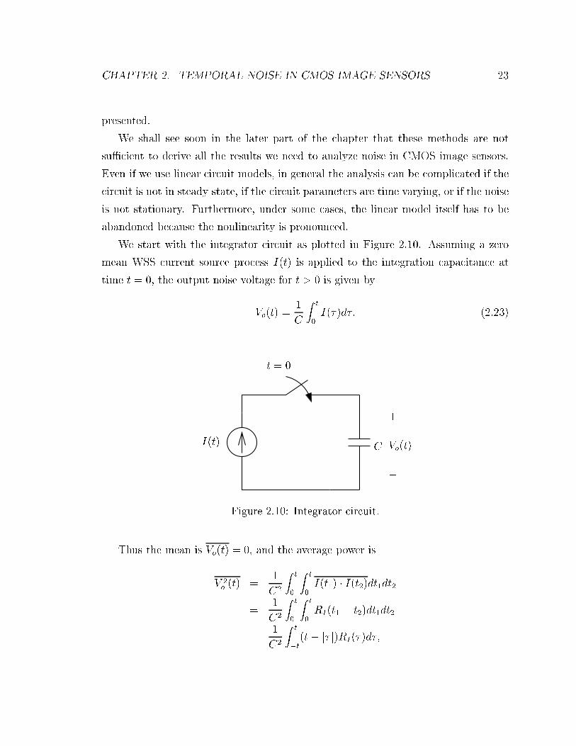
We start with the integrator circuit as plotted in Figure 2.10. Assuming a zero
mean WSS current source process I(t) is applied to the integration capacitance at
time t = 0, the output noise voltage for t > 0 is given by
Vo(t) =1
C
Zt
0I(�)d�: (2.23)
I(t)
t = 0
C Vo(t)
+
�
Figure 2.10: Integrator circuit.
Thus the mean is Vo(t) = 0, and the average power is
V 2o(t) =
1
C2
Zt
0
Zt
0I(t1) � I(t2)dt1dt2
=1
C2
Zt
0
Zt
0RI(t1 � t2)dt1dt2
=1
C2
Zt
�t
(t� j� j)RI(�)d�;
CHAPTER 2. TEMPORAL NOISE IN CMOS IMAGE SENSORS 24
X(t) Y (t)h(t)
Figure 2.11: Linear time invariant circuit.
where RI(�) is the process autocorrelation function. If I(t) is a white noise process
with psd P
2, then RI(�) =
P
2Æ(�) and
V 2o(t) =
1
C2
Zt
�t
(t� j� j)P
2Æ(�)d� (2.24)
=P
2C2t (2.25)
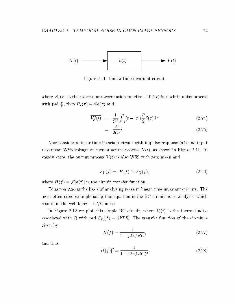
Now consider a linear time invariant circuit with impulse response h(t) and input
zero mean WSS voltage or current source process X(t), as shown in Figure 2.11. In
steady state, the output process Y (t) is also WSS with zero mean and
SY (f) = jH(f)j2 � SX(f); (2.26)
where H(f) = F [h(t)] is the circuit transfer function.
Equation 2.26 is the basis of analyzing noise in linear time invariant circuits. The
most often cited example using this equation is the RC circuit noise analysis, which
results in the well known kT/C noise.
In Figure 2.12 we plot this simple RC circuit, where Vi(t) is the thermal noise
associated with R with psd SVi(f) = 2kTR. The transfer function of the circuit is
given by
H(f) =1
1 + j2�fRC; (2.27)
and thus
jH(f)j2 =1
1 + (2�fRC)2: (2.28)
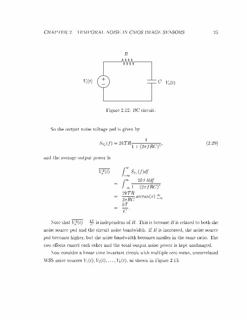
CHAPTER 2. TEMPORAL NOISE IN CMOS IMAGE SENSORS 25
Vi(t) Vo(t)C
R
+
�
Figure 2.12: RC circuit.
So the output noise voltage psd is given by
SVo(f) = 2kTR1
1 + (2�fRC)2; (2.29)
and the average output power is
V 2o(t) =
Z1
�1
SVo(f)df
=
Z1
�1
2kTRdf
1 + (2�fRC)2
=2kTR
2�RCarctan(x)j1
�1
=kT
C:
Note that V 2o(t) = kT
Cis independent of R. This is because R is related to both the
noise source psd and the circuit noise bandwidth. If R is increased, the noise source
psd becomes higher, but the noise bandwidth becomes smaller in the same ratio. The
two e�ects cancel each other and the total output noise power is kept unchanged.
Now consider a linear time invariant circuit with multiple zero mean, uncorrelated
WSS noise sources V1(t); V2(t); : : : ; Vk(t), as shown in Figure 2.13.
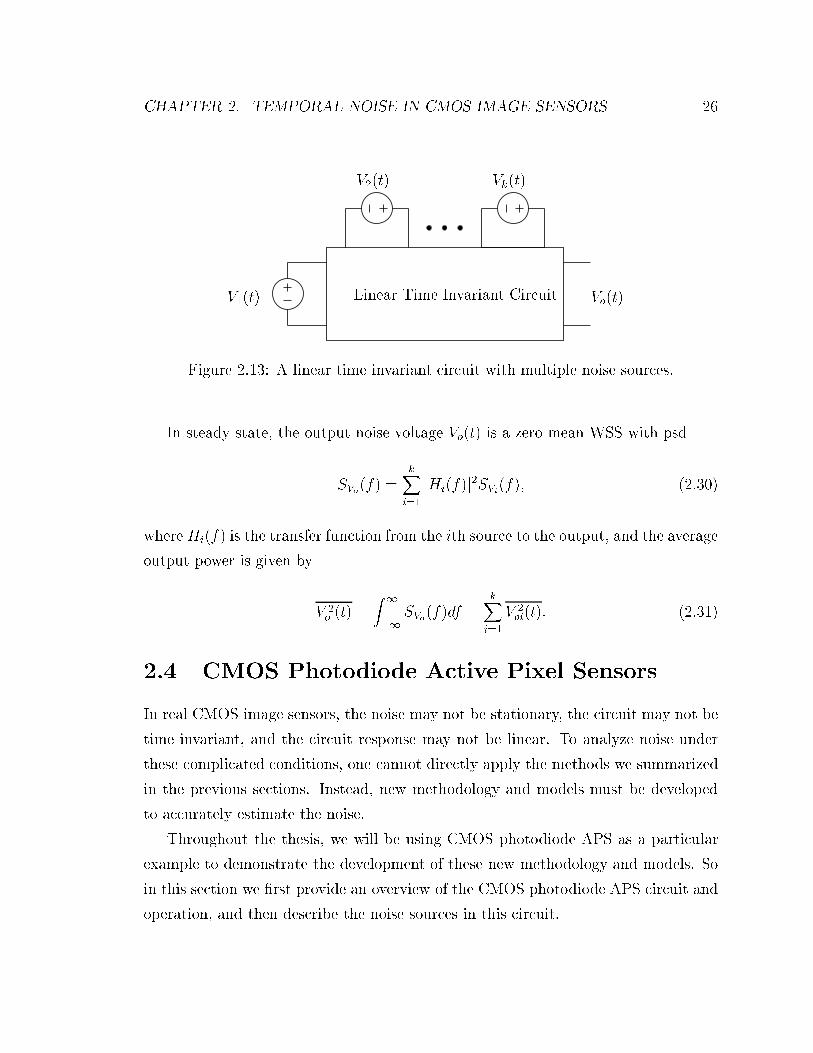
CHAPTER 2. TEMPORAL NOISE IN CMOS IMAGE SENSORS 26
Linear Time Invariant CircuitV1(t)
V2(t) Vk(t)
Vo(t)
Figure 2.13: A linear time invariant circuit with multiple noise sources.
In steady state, the output noise voltage Vo(t) is a zero mean WSS with psd
SVo(f) =kXi=1
jHi(f)j2SVi(f); (2.30)
where Hi(f) is the transfer function from the ith source to the output, and the average
output power is given by
V 2o(t) =
Z1
�1
SVo(f)df =kXi=1
V 2oi(t): (2.31)
2.4 CMOS Photodiode Active Pixel Sensors
In real CMOS image sensors, the noise may not be stationary, the circuit may not be
time invariant, and the circuit response may not be linear. To analyze noise under
these complicated conditions, one cannot directly apply the methods we summarized
in the previous sections. Instead, new methodology and models must be developed
to accurately estimate the noise.
Throughout the thesis, we will be using CMOS photodiode APS as a particular
example to demonstrate the development of these new methodology and models. So
in this section we �rst provide an overview of the CMOS photodiode APS circuit and
operation, and then describe the noise sources in this circuit.
CHAPTER 2. TEMPORAL NOISE IN CMOS IMAGE SENSORS 27
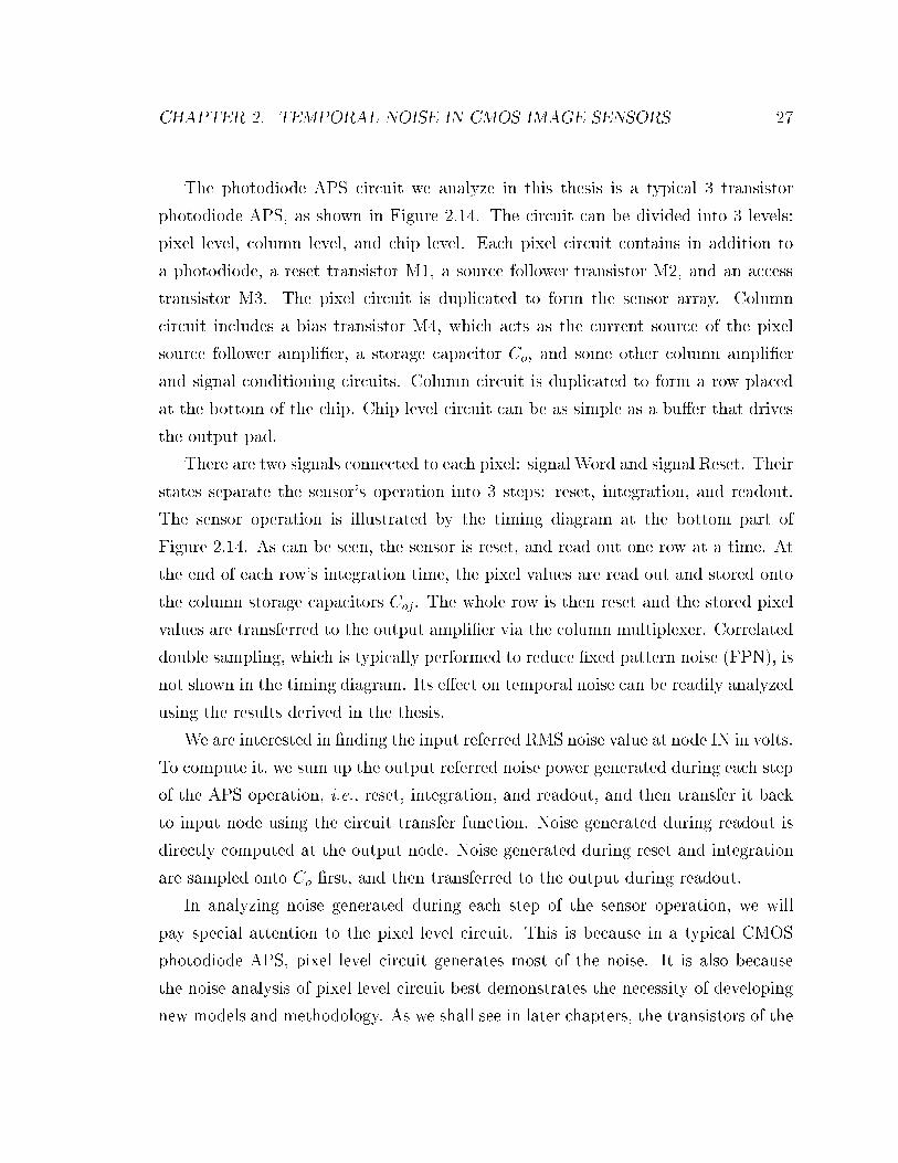
The photodiode APS circuit we analyze in this thesis is a typical 3 transistor
photodiode APS, as shown in Figure 2.14. The circuit can be divided into 3 levels:
pixel level, column level, and chip level. Each pixel circuit contains in addition to
a photodiode, a reset transistor M1, a source follower transistor M2, and an access
transistor M3. The pixel circuit is duplicated to form the sensor array. Column
circuit includes a bias transistor M4, which acts as the current source of the pixel
source follower ampli�er, a storage capacitor Co, and some other column ampli�er
and signal conditioning circuits. Column circuit is duplicated to form a row placed
at the bottom of the chip. Chip level circuit can be as simple as a bu�er that drives
the output pad.
There are two signals connected to each pixel: signal Word and signal Reset. Their
states separate the sensor's operation into 3 steps: reset, integration, and readout.
The sensor operation is illustrated by the timing diagram at the bottom part of
Figure 2.14. As can be seen, the sensor is reset, and read out one row at a time. At
the end of each row's integration time, the pixel values are read out and stored onto
the column storage capacitors Coj. The whole row is then reset and the stored pixel
values are transferred to the output ampli�er via the column multiplexer. Correlated
double sampling, which is typically performed to reduce �xed pattern noise (FPN), is
not shown in the timing diagram. Its e�ect on temporal noise can be readily analyzed
using the results derived in the thesis.
We are interested in �nding the input referred RMS noise value at node IN in volts.
To compute it, we sum up the output referred noise power generated during each step
of the APS operation, i.e., reset, integration, and readout, and then transfer it back
to input node using the circuit transfer function. Noise generated during readout is
directly computed at the output node. Noise generated during reset and integration
are sampled onto Co �rst, and then transferred to the output during readout.
In analyzing noise generated during each step of the sensor operation, we will
pay special attention to the pixel level circuit. This is because in a typical CMOS
photodiode APS, pixel level circuit generates most of the noise. It is also because
the noise analysis of pixel level circuit best demonstrates the necessity of developing
new models and methodology. As we shall see in later chapters, the transistors of the
CHAPTER 2. TEMPORAL NOISE IN CMOS IMAGE SENSORS 28
Pixel (i,j) Column Amp/Cap/Mux Output Ampli�er
Reset i
Reset i
Word i
Word i
Bit j
CojVbias
Col j
Col j
Out
M1M2
M3
M4
IN
Word i+1
Reset i+1
Row i Read
Integration Time
Figure 2.14: CMOS photodiode APS circuit and timing diagram.
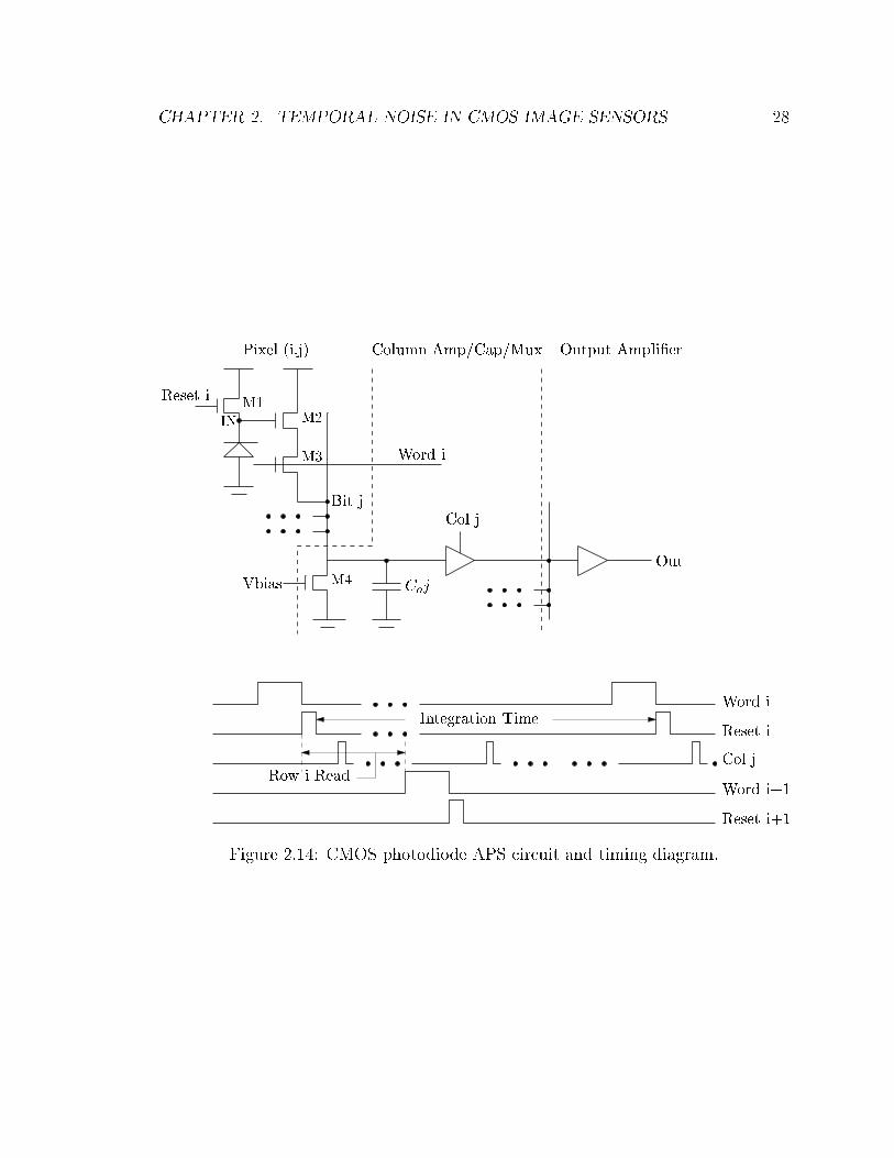
CHAPTER 2. TEMPORAL NOISE IN CMOS IMAGE SENSORS 29
circuit model circuit model
Steady state Non-steady state
Stationary noise
Nonstationary noise
Follower (thermal)
Access (thermal)Photodiode (shot)
Follower (1/f)
Access (1/f)Reset (shot, 1/f)
Figure 2.15: Noise sources in CMOS APS pixel level circuit.
pixel level circuit work at almost every possible regime, including saturation, linear,
and subthreshold. They also cover all the combinations of steady/nonsteady state
circuit and stationary/nonstationary noise sources. Even worse, the pixel circuit is
quite nonlinear during the integration time.
Figure 2.15 summarizes the noise sources presented in a typical CMOS APS pixel
level circuit. As can be seen, the analysis of shot and 1/f noise due to the reset
transistor is particularly complicated, involving both a nonsteady state circuit model
(actually time varying) and a nonstationary noise source. By comparison, the ther-
mal noise due to the follower and the access transistor can be accurately estimated
using the stationary noise sources and steady state circuit models. This is the on-
ly combination in the �gure that has been accurately analyzed by the conventional
frequency domain noise analysis methods. In the thesis, we will develop methods to
better estimate noise e�ects for all other 3 combinations.
In the following chapters, we will analyze thermal noise and shot noise, using time
domain noise analysis method to deal with the time varying circuits. Analysis of 1/f
noise then follows. Since the current 1/f noise models are not suÆcient to handle
switched circuits, we will start from the basic theorem to derive a nonstationary 1/f
noise model �rst, and then use it to analyze 1/f noise in CMOS APS.
CHAPTER 2. TEMPORAL NOISE IN CMOS IMAGE SENSORS 30
2.5 Summary
We reviewed the basic math background that is necessary for noise analysis, including
random variables and random processes. We then go over the often used circuit noise
analysis models and methods, such as the noise models for fundamental noise sources
in integrated circuits, the noise models for basic semiconductor devices in CMOS
image sensors, and the methods to analyze noise in a linear circuit. CMOS photodiode
APS circuit is then presented together with its operation and noise sources. We note
that the pixel level circuit generates most of the noise, and involves all combinations
of steady/nonsteady state circuit models and stationary/nonstationary noise sources.
It is a good example to demonstrate the necessity of developing new models and
methodology to analyze noise in CMOS image sensors, and will be used throughout
the thesis.
Chapter 3
Analysis of Thermal and Shot
Noise in CMOS APS
3.1 Introduction
Hand analysis of thermal and shot noise in CCDs and CMOS APS have been pub-
lished by several authors [49, 19, 23, 3, 56, 34, 5]. Their analysis shows that at low
illumination the dominant source of noise is reset and readout transistors thermal and
shot noise, while at high illumination the dominant source of noise is the photodiode
shot noise. The noise power due to the reset transistor, which is sampled at the end
of reset, is often quoted to be kT
CV2. Recent experiments [57, 45], however, showed
that the measured reset noise is signi�cantly smaller than kT
C. In analyzing noise due
to photodiode shot noise it is often assumed that the photodiode charge to voltage
relation is linear. As supply voltage scales with CMOS technology this relation is
becoming increasingly nonlinear.
In this chapter we present a detailed and rigorous analysis of noise due to ther-
mal and shot noise sources in photodiode APS that takes into consideration these
complicating factors. We show that during reset the reset transistor operates in sub-
threshold and steady state is not achieved. As a result, the conventional frequency
domain noise analysis method cannot be applied. To calculate reset noise power we
consider the time varying reset circuit model and perform time-domain noise analysis
31
CHAPTER 3. ANALYSIS OF THERMAL AND SHOT NOISE IN CMOS APS 32
using the MOS transistor subthreshold noise model [53]. We show that reset noise
power is at most half of its commonly quoted kT
Cvalue, which corroborates the pub-
lished experimental results. The lower reset noise, however, comes at the expense of
image lag. Since steady state is not reached during reset, the �nal photodiode reset
voltage depends on its initial value. This problem can be alleviated by overdriving
the gate of the reset transistor or by using a pMOS instead of an nMOS transistor
for reset. These techniques, however, double the reset noise power. We propose a
new \pseudo- ash" reset method, which can alleviate image lag without increasing
reset noise. We then present an analysis of photodiode shot noise that takes into
consideration the nonlinearity of the photodiode charge to voltage conversion. We
again perform time-domain noise analysis using a time varying circuit model. We
�nd that the nonlinearity actually improves SNR at high illumination.
The rest of the chapter is organized as follows. In section 3.2 we present our
analysis of reset noise using time domain analysis. In section 3.3 we discuss the image
lag due to incomplete reset and present our pseudo- ash reset method. In section 3.4
we present the analysis of the photodiode shot noise that takes into consideration
the nonlinearity of the photodiode charge to voltage conversion. In section 3.5 we
use SPICE to estimate the noise contributions of the follower, access and column
ampli�er transistors. We �nd that the contributions of these transistors to the noise
is negligible compared to reset and photodiode shot noise.
3.2 Noise Due to Reset
During reset the gate of the reset transistor M1 is set to a high voltage, typically
vdd. At the beginning of reset, M1 is either operating in the saturation region or in
subthreshold depending on the photodiode voltage at the end of integration. If the
photodiode voltage is low enough, M1 is in saturation at �rst and for a very short
amount of time before it goes into subthreshold for the rest of reset. Note that this
source follower reset circuit con�guration and operation is widely used also in CCD
image sensors to implement the output stage reset.
The circuit noise model during reset is shown in Figure 3.1. The current source
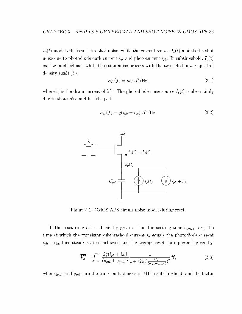
CHAPTER 3. ANALYSIS OF THERMAL AND SHOT NOISE IN CMOS APS 33
Id(t) models the transistor shot noise, while the current source Is(t) models the shot
noise due to photodiode dark current idc and photocurrent iph. In subthreshold, Id(t)
can be modeled as a white Gaussian noise process with the two sided power spectral
density (psd) [53]
SId(f) = qid A2/Hz; (3.1)
where id is the drain current of M1. The photodiode noise source Is(t) is also mainly
due to shot noise and has the psd
SIs(f) = q(iph + idc) A2/Hz: (3.2)
tr
vdd
id(t) + Id(t)
vo(t)
Cpd Is(t) iph + idc
Figure 3.1: CMOS APS circuit noise model during reset.
If the reset time tr is suÆciently greater than the settling time tsettle, i.e., the
time at which the transistor subthreshold current id equals the photodiode current
iph + idc, then steady state is achieved and the average reset noise power is given by
V 2n=
Z1
�1
2q(iph + idc)
(gm1 + gmb1)21
1 + (2�fCpd
(gm1+gmb1))2df; (3.3)
where gm1 and gmb1 are the transconductances of M1 in subthreshold, and the factor
CHAPTER 3. ANALYSIS OF THERMAL AND SHOT NOISE IN CMOS APS 34
of 2 is due to the fact that in steady state id = iph + idc. Performing the integral we
get that
V 2n=
q(iph + idc)
Cpd(gm1 + gmb1): (3.4)
Since in subthreshold id =kT
q(gm1+ gmb1), we get V 2
n= kT
Cpd, which is the same as the
often quoted reset noise value.
This analysis, however, holds only if steady state is achieved during reset, which
can only occur if the settling time is shorter than the reset time. To �nd out whether
the circuit is in steady state, we need compute the settling time tsettle. Applying
Kirchho�'s current law we get that
dVpd(t)
dt=id(t) + In(t)� iph � idc
Cpd(Vpd(t)); (3.5)
where In(t) = Id(t) + Is(t) and Vpd is the photodiode voltage. Assuming that the
signal is much larger than the noise, which is true for the circuit we analyze, we can
express the photodiode voltage during reset as the sum of a signal voltage vpd(t) and
a noise voltage Vn(t), i.e., Vpd(t) = vpd(t) + Vn(t), and approximate the capacitance
Cpd(Vpd(t)) � Cpd(vpd(t)) +dCpd
dvpdVn(t). With these approximations, we can write the
signal part of equation 3.5 as
dvpd(t)
dt= �
iph + idc
Cpd(vpd(t))+
id(vpd(t))
Cpd(vpd(t)): (3.6)
To calculate settling time using this equation, we need �rst �nd the time t1 at
which the reset transistor transitions from above to below threshold. The reset tran-
sistor then operates in subthreshold for a period of t2 = tsettle � t1 until it reaches
steady state, i.e., until its drain current almost equals iph + idc.
While the reset transistor is operating above threshold, its drain current is given
by [35]
id(t) =W
2LCox�n(vdd � vth(vpd)� vpd)
2; (3.7)
where W and L are the transistor channel width and length, Cox is the gate oxide
capacitance (per unit area), �n is the electron mobility, and vth is the threshold
CHAPTER 3. ANALYSIS OF THERMAL AND SHOT NOISE IN CMOS APS 35
voltage.
Note here vth is also a function of vpd
vth(vpd) = vth0 + (qvpd + 2j�pj �
q2j�pj) V; (3.8)
where vth0 is the threshold voltage at 0V source-substrate bias, is the body e�ect
parameter, and �p is the bulk potential.
For most of the reset time M1 operates in subthreshold, and id can be expressed
as [31]
id(t) =W
LI0e
h(vg�vpd)�
vT
�(vpd
�vb)(1��)
vT
i(1� e
�(vd�v
pd)
vT ); (3.9)
where vg is the gate voltage, vd is the drain voltage, vpd is the source voltage, vb is
the bulk voltage, � is the gate eÆciency factor, vT = kT
q, and I0 is a constant that
depends on the transistor threshold voltage.
The transition between above and below threshold occurs when the currents cal-
culated using equations 3.7 and 3.9 are equal. Assuming the circuit parameters of
the test structure which will be described in chapter 4, we �nd that the transition
voltage v1, i.e., the voltage at which this transition occurs, � 2V. The transition time
t1 is � 0:2ns even when the photodiode voltage vpd(0) is very low.
To �nd t2, we �rst set v1 = 2V and assume that the capacitance Cpd(vpd(t)) = Cpd,
i.e., is independent of t. De�ning K0 =W
LI0e
vg�
vT and substituting from equation 3.9
into equation 3.6 then solving it, we get that
vpd(t) = vT ln�K0 +K0e
ict
vT Cpd + icev1vT
iceict
vTCpd
; (3.10)
where ic = iph + idc, and the time origin is shifted such that t = 0 corresponds to the
time when the reset transistor enters subthreshold.
Combining equations 3.10 and 3.9 we can explicitly write id(t) as a function of
time. Now assuming that steady state is achieved for id(t) � ic we �nd that
t2 =vTCpd
icln
K0
icev1vT �K0
: (3.11)
CHAPTER 3. ANALYSIS OF THERMAL AND SHOT NOISE IN CMOS APS 36
Thus we get the settling time tsettle = t1 + t2, which is more than 1ms for typical
illumination conditions.
Figure 3.2 plots the settling time as a function of photocurrents, which shows that
tsettle � 1ms even for very high photocurrents. This settling time is much larger than
the typical reset time, which is typically in the few microseconds range. Therefore
steady state is not achieved during reset and we must analyze the reset noise for a
time varying circuit model using time domain analysis.
iph + idc (fA)
settlingtime(ms)
00 100 200 300 400 500 600
2
4
6
8
10
12
14
16
18
20
Figure 3.2: Reset settling time tsettle vs. photodiode current.
To perform this time domain analysis, �rst note that id is a function of (vpd(t) +
Vn(t)). Linearizing around the signal voltage vpd(t) we get that id(t) � id(vpd(t)) �
g(t)Vn(t), where g(t) = �did
dvpdis the total transistor transconductance. Also note that
during reset the photodiode capacitance changes very little, and thus we can write
CHAPTER 3. ANALYSIS OF THERMAL AND SHOT NOISE IN CMOS APS 37
Cpd(Vpd(t)) � Cpd(vpd(t)). The noise part of equation 3.5 is thus given by
In(t) = Cpd(vpd(t))dVn(t)
dt+ g(t)Vn(t): (3.12)
Note that this is a general �rst order linear di�erential equation and the solution
at the end of reset can be expressed as a functional of the noise source current
Vn(tr) =
Ztr
0
In(�)
Cpd(�)e�
Rtr
�
g(�0)
Cpd(�0)d�0d�: (3.13)
When the noise autocorrelation function is a Æ function, which is the case for
thermal and shot noise we get that
V 2n(tr) =
Ztr
0
R(�)
C2pd(�)
e�2Rtr
�
g(�0)
Cpd
(�0)d�0d�; (3.14)
where R(�) is the psd of the (white) noise source. For a more general noise process,
a similar formula was derived in [50].
It can be readily veri�ed from equation 3.14 that the contribution from the noise
above threshold is extremely small, and can thus be ignored. We can also ignore the
shot noise associated with iph + idc, since these currents are much smaller than the
reset transistor drain current. With these simplifying assumptions, R(�) = qid(�),
and Cpd(�) is a constant, which we denote by Cpd.
To �nd V 2n(tr), we need to evaluate the inner integral in equation 3.14. To calculate
g(t), we need to calculate the signal voltage vpd(t) �rst. Given that iph+ idc << id(t),
we can approximate equation 3.10 by
vpd(t) � vT ln(K0t
vTCpd
+ ev1vT ); (3.15)
where vT = kT
q, K0 =
W
LI0e
vg�
vT , v1 is the transition voltage, and t = 0 corresponds
to the time when the reset transistor enters subthreshold. We let Æ =vTCpd
id(0)be the
thermal time, i.e., the time to charge the photodiode capacitance to vT using id(0).
Substituting in the I{V characteristics of the MOS transistor in subthreshold, we get
CHAPTER 3. ANALYSIS OF THERMAL AND SHOT NOISE IN CMOS APS 38
that
id(�) �vTCpd
� + Æ: (3.16)
Now evaluating the inner integral in equation 3.14 with tr � t1 replacing tr, and
g(t) =id(t)
vTwe get that
Ztr�t1
�
g(�0)
Cpd(�0)d�0 =
Ztr�t1
�
1
�0 + Æd�0 = ln
tr � t1 + Æ
� + Æ: (3.17)
Substituting into equation 3.14, we get the mean square noise voltage at the end of
reset
V 2n(tr) =
1
2
kT
Cpd
(1�Æ2
(tr � t1 + Æ)2): (3.18)
Thus the mean square reset noise voltage is less than 12of the often quoted kT
Cpdvalue.
Since tr is typically in the few microsecond range, while t1 � 0:2ns and Æ � 6ns for
our test structure circuit, the mean square reset noise voltage value is in fact very
close to kT
2Cpd. For example assuming Cpd = 22fF, which is consistent with the circuit
in our test structure discussed in section 4.3, we get an input referred RMS reset noise
voltage of 303�V at room temperature.
The intuitive reason for the kT
2Cpdresult is twofold. First, by inspecting equa-
tion 3.14 we see that the noise decays exponentially while it is being integrated onto
Cpd. In subthreshold where the transistor I{V relation is exponential, the decay and
integration balance each other and the the circuit is in \virtual" steady state. The
second reason is that in the case we are considering, shot noise due to the reset
transistor drain current dominates, which in steady state contributes only kT
2Cpd[42].
If reset time is long enough steady state is eventually reached. In this case, the
noise power should become kT
Cpdas calculated using conventional frequency domain
analysis. Now we show that time domain analysis gives the same result.
When steady state is reached, the noise due to the photodiode photo and dark
currents can no longer be ignored. To simplify notation we de�ne i0d= iph + idc. The
autocorrelation function of the shot noise due to both the reset transistor and the
CHAPTER 3. ANALYSIS OF THERMAL AND SHOT NOISE IN CMOS APS 39
photodiode is thus given by
R(t) =
8<: qid(t) + qi0
dt < tsettle
2qi0d; t � tsettle:
(3.19)
Now de�ne g0 =qi0
d
kT, then for t � tsettle g(t) = g0. Using equation 3.14 we get the
mean square noise voltage
V 2n(tr) =
Ztsettle
0
qid(�) + qi0d
C2pd
e�2Rtr
�
g(�0)
Cpd
d�0d� +
Ztr
tsettle
2qi0d
C2pd
e�2Rtr
�
g0
Cpd
d�0d�
=
Ztset
0
qid(�)
C2pd
e�2Rtr
�
g(�0)
Cpd
d�0d� +
Ztset
0
qi0d
C2pd
e�2Rtr
�
g(�0)
Cpd
d�0d�
+
Ztr
tset
2qi0d
C2pd
e�2Rtr
�
g0
Cpd
d�0d�
=
Ztsettle
0
qid(�)
C2pd
e�2Rtsettle
�
g(�0)
Cpd
d�0d� e
�2Rtr
tsettle
g0
Cpd
d�0
+qi0d
C2pd
Ztsettle
0
(� + Æ)2
(tsettle � t1 + Æ)2d� e
�2Rtr
tsettle
g0
Cpd
d�0
+2qi0
d
C2pd
Ztr
tsettle
e�2
g0
Cpd
(tr��)d�: (3.20)
Using the same method that we derived equation 3.18, equation 3.20 can be sim-
pli�ed into
V 2n(tr) =
1
2
kT
Cpd
(1�Æ2
(tsettle � t1 + Æ)2) e
�2g0
Cpd
(tr�tsettle)
+1
3
qi0d
C2pd
((tsettle � t1 + Æ)�Æ3
(tsettle � t1 + Æ)2) e
�2g0
Cpd
(tr�tsettle)
+kT
Cpd
(1� e�2
g0
Cpd
(tr�tsettle)) (3.21)
�1
2
kT
Cpd
e�2
g0
Cpd
(tr�tsettle)+1
3
qi0dtsettle
C2pd
e�2
g0
Cpd
(tr�tsettle)
+kT
Cpd
(1� e�2
g0
Cpd
(tr�tsettle)):
CHAPTER 3. ANALYSIS OF THERMAL AND SHOT NOISE IN CMOS APS 40
The �rst term of the above equation is due to the reset transistor shot noise during
the non-steady state period. Similarly, the second term is due to the photodiode
shot noise noise during the non-steady state period. Using i0d= id(tsettle) �
vTCpd
tsettle+Æ
(equation 3.16), we get that 13
qi0
dtsettle
C2pd
�13kT
Cpd. As expected the second term is smaller
than the �rst, since for t < tsettle i0
d< id(t). The last term represents the noise
generated during t � tsettle.
As tr !1, e�2
g0
Cpd
(tr�tsettle)approaches zero and the �rst two terms vanish. This
con�rms that the noise generated before tsettle �nally decays to zero. The last term on
the other hand approaches kT
Cpd, which is the same as the steady state result obtained
using frequency domain analysis.
We now verify that the above derivation also leads to kT
2Cpdfor t � tsettle. It is
clear that in this case the third term of equation 3.21 does not exist. The second
term can be ignored, since i0d� id(tr),
13
qi0
dtr
C2pd
�13kT
Cpd. This leaves us with the �rst
term which is equal to the right-hand side of equation 3.18.
3.3 Image Lag Due to Incomplete Reset
In the previous section we found that reset noise power is at most half of its commonly
quoted kT
Cvalue. This reduction in noise, however, comes at the expense of image
lag. Since steady state is not reached, the �nal reset voltage can depend on the
photodiode voltage at the beginning of reset, and thus resulting in image lag. Note
that the source of image lag here is di�erent from the source of image lag in CCDs,
where image lag is caused by incomplete charge transfer and can be eliminated using
a pinned photodiode [48]. In this section, we explore the image lag problem in CMOS
APS, and propose a new reset method, which alleviates lag without increasing reset
noise.
To analyze image lag we assume the standard APS circuit and operation described
in section 2.4. In Figure 3.3, we plot the simulated photodiode voltage waveform for
four di�erent frame to frame illumination conditions assuming integration time tint =
30ms, reset time tr = 1�s, dark current idc = 2:3fA, and bright level photocurrent
iph = 50fA. The bright condition in the �gure refers to the case where the photodiode
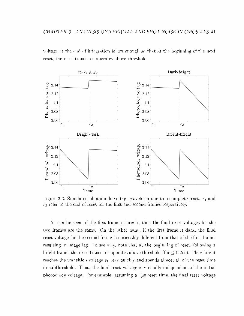
CHAPTER 3. ANALYSIS OF THERMAL AND SHOT NOISE IN CMOS APS 41
voltage at the end of integration is low enough so that at the beginning of the next
reset, the reset transistor operates above threshold.
Dark-dark
Photodiodevoltage
r1 r22.06
2.08
2.1
2.12
2.14
Dark-bright
Photodiodevoltage
r1 r22.06
2.08
2.1
2.12
2.14
Bright-dark
Photodiodevoltage
Timer1 r2
2.06
2.08
2.1
2.12
2.14
Bright-bright
Photodiodevoltage
Timer1 r2
2.06
2.08
2.1
2.12
2.14
Figure 3.3: Simulated photodiode voltage waveform due to incomplete reset. r1 and
r2 refer to the end of reset for the �rst and second frames respectively.
As can be seen, if the �rst frame is bright, then the �nal reset voltages for the
two frames are the same. On the other hand, if the �rst frame is dark, the �nal
reset voltage for the second frame is noticeably di�erent from that of the �rst frame,
resulting in image lag. To see why, note that at the beginning of reset, following a
bright frame, the reset transistor operates above threshold (for � 0:2ns). Therefore it
reaches the transition voltage v1 very quickly and spends almost all of the reset time
in subthreshold. Thus, the �nal reset voltage is virtually independent of the initial
photodiode voltage. For example, assuming a 1�s reset time, the �nal reset voltage
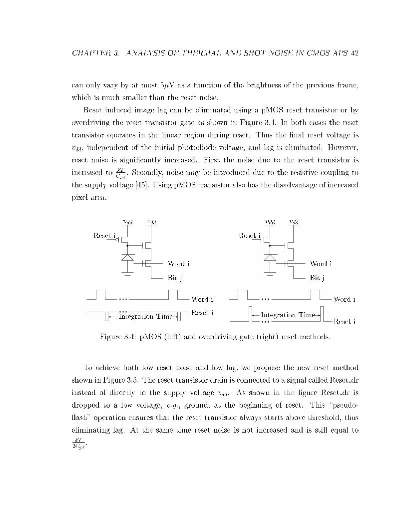
CHAPTER 3. ANALYSIS OF THERMAL AND SHOT NOISE IN CMOS APS 42
can only vary by at most 5�V as a function of the brightness of the previous frame,
which is much smaller than the reset noise.
Reset induced image lag can be eliminated using a pMOS reset transistor or by
overdriving the reset transistor gate as shown in Figure 3.4. In both cases the reset
transistor operates in the linear region during reset. Thus the �nal reset voltage is
vdd, independent of the initial photodiode voltage, and lag is eliminated. However,
reset noise is signi�cantly increased. First the noise due to the reset transistor is
increased to kT
Cpd. Secondly, noise may be introduced due to the resistive coupling to
the supply voltage [45]. Using pMOS transistor also has the disadvantage of increased
pixel area.
Reset iReset i
Reset i
Reset i
Word i
Word i
Word i
Word i
Bit j Bit j
Integration TimeIntegration Time
vddvdd vdd vdd
Figure 3.4: pMOS (left) and overdriving gate (right) reset methods.
To achieve both low reset noise and low lag, we propose the new reset method
shown in Figure 3.5. The reset transistor drain is connected to a signal called Reset dr
instead of directly to the supply voltage vdd. As shown in the �gure Reset dr is
dropped to a low voltage, e.g., ground, at the beginning of reset. This \pseudo-
ash" operation ensures that the reset transistor always starts above threshold, thus
eliminating lag. At the same time reset noise is not increased and is still equal to
kT
2Cpd.
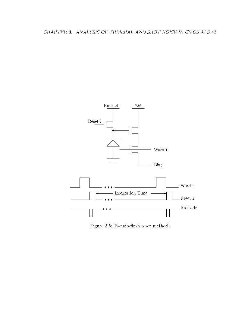
CHAPTER 3. ANALYSIS OF THERMAL AND SHOT NOISE IN CMOS APS 43
Reset dr
Reset dr vdd
Reset i
Reset i
Word i
Word i
Bit j
Integration Time
Figure 3.5: Pseudo- ash reset method.
CHAPTER 3. ANALYSIS OF THERMAL AND SHOT NOISE IN CMOS APS 44
3.4 Noise Due to Integration
During integration, shot noise due to the dark current idc and photocurrent iph dom-
inates, with psd SIs(f) = q(iph + idc) A2/Hz. To analyze noise generated during
integration we again consider equation 3.5 but with the reset transistor turned o�. If
we assume that the photodiode capacitance is constant over the integration time, it
is easy to show that the mean square value of the noise voltage sampled at the end
of integration, i.e., at tint, is given by
V 2n(tint) =
q(iph + idc)
C2pd
tint: (3.22)
The photodiode capacitance, however, is a function of its reverse bias voltage and
can thus change signi�cantly over integration time. So again we need to perform
time-domain noise analysis.
Assuming that the noise is much smaller than the signal, we can write the noise
part of equation 3.5 as
In(t) = Is(t) = Cpd(vpd(t))dVn(t)
dt+ gc(t)Vn(t); (3.23)
where
gc(t) = �1
Cpd(vpd(t))
dCpd(vpd(t))
dvpd(t)(iph + idc)
is the varying capacitance induced conductance. Unlike the reset noise case, here we
cannot ignore this conductance, because now vpd varies in 1V range and thus gc(t)
can be fairly large.
Equation 3.23 again is a general �rst order linear di�erential equation and the
mean square value of Vn at the end of integration is given by
V 2n(tint) = q(iph + idc)
Ztint
0
1
C2pd(vpd(�))
e�2(iph+idc)
Rtint
�
d(1=Cpd
(vpd
(�0)))
dvpd
(�0)d�0d�: (3.24)
Note that equation 3.22 follows from this more general equation if we assume
that Cpd is constant during integration. To take the dependency of the photodiode
CHAPTER 3. ANALYSIS OF THERMAL AND SHOT NOISE IN CMOS APS 45
capacitance on the reverse bias voltage into consideration, we make the simplifying
assumption of an abrupt pn junction to get that
Cpd(vpd(t)) = Cpd(vpd(0))
vuutvpd(0) + �
vpd(t) + �; (3.25)
where � is the built in junction potential, and vpd(0) is the voltage on Cpd at the
beginning of integration.
The signal part of equation 3.5 during integration can be written as
dvpd(t)
dt= �
iph + idc
Cpd(vpd(t)): (3.26)
Solving equation 3.26 we get that
vpd(t) = vpd(0)�(iph + idc)
Cpd(vpd(0))t+
(iph + idc)2t2
4C2pd(vpd(0))(vpd(0) + �)
: (3.27)
The square term in equation 3.27 shows that the signal is actually reduced by the
nonlinearity.
We can now explicitly express Cpd(vpd(t)) as a function of t to get
Cpd(vpd(t)) = Cpd(vpd(0))1
1�(iph+idc)t
2Cpd(vpd(0))(vpd(0)+�)
: (3.28)
Thus we have
d(1=Cpd(vpd(t)))
dvpd(t)=
1
Cpd(vpd(0))
1
2(vpd(0) + �)�iph+idc
Cpd(vpd(0))t: (3.29)
Substituting equations 3.27, 3.28, and 3.29 into equation 3.24, we get that the
mean square noise voltage at the end of integration is given by
V 2n(tint) =
q(iph + idc)
C2pd(vpd(0))
tint(1�1
2(vpd(0) + �)
iph + idc
Cpd(vpd(0))tint)
2: (3.30)
To demonstrate the e�ect of varying capacitance during integration, we consider
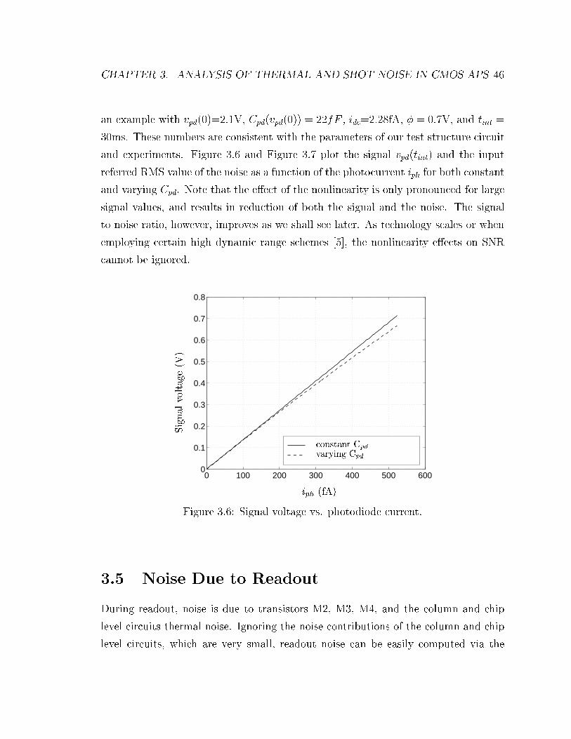
CHAPTER 3. ANALYSIS OF THERMAL AND SHOT NOISE IN CMOS APS 46
an example with vpd(0)=2.1V, Cpd(vpd(0)) = 22fF , idc=2.28fA, � = 0:7V, and tint =
30ms. These numbers are consistent with the parameters of our test structure circuit
and experiments. Figure 3.6 and Figure 3.7 plot the signal vpd(tint) and the input
referred RMS value of the noise as a function of the photocurrent iph for both constant
and varying Cpd. Note that the e�ect of the nonlinearity is only pronounced for large
signal values, and results in reduction of both the signal and the noise. The signal
to noise ratio, however, improves as we shall see later. As technology scales or when
employing certain high dynamic range schemes [5], the nonlinearity e�ects on SNR
cannot be ignored.
0 100 200 300 400 500 6000
0.1
0.2
0.3
0.4
0.5
0.6
0.7
0.8
iph (fA)
Signalvoltage(V)
constant Cpdvarying Cpd
Figure 3.6: Signal voltage vs. photodiode current.
3.5 Noise Due to Readout
During readout, noise is due to transistors M2, M3, M4, and the column and chip
level circuits thermal noise. Ignoring the noise contributions of the column and chip
level circuits, which are very small, readout noise can be easily computed via the
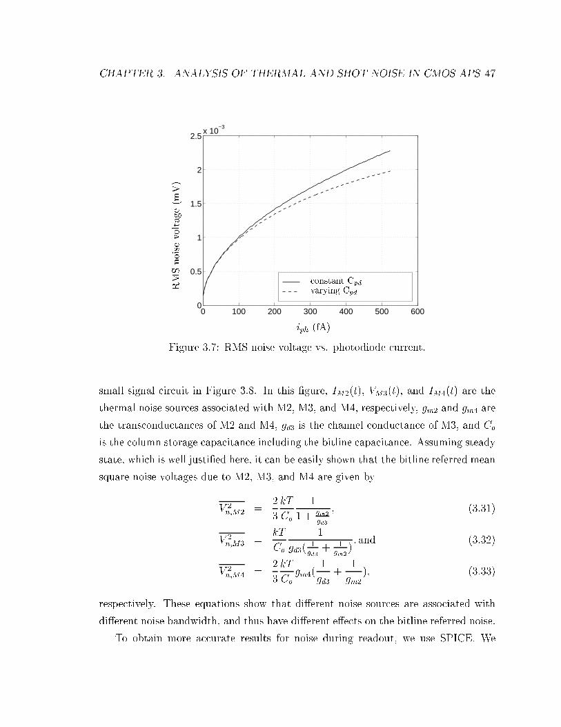
CHAPTER 3. ANALYSIS OF THERMAL AND SHOT NOISE IN CMOS APS 47
0 100 200 300 400 500 6000
0.5
1
1.5
2
2.5x 10
−3
iph (fA)
RMSnoisevoltage(mV)
constant Cpdvarying Cpd
Figure 3.7: RMS noise voltage vs. photodiode current.
small signal circuit in Figure 3.8. In this �gure, IM2(t), VM3(t), and IM4(t) are the
thermal noise sources associated with M2, M3, and M4, respectively, gm2 and gm4 are
the transconductances of M2 and M4, gd3 is the channel conductance of M3, and Co
is the column storage capacitance including the bitline capacitance. Assuming steady
state, which is well justi�ed here, it can be easily shown that the bitline referred mean
square noise voltages due to M2, M3, and M4 are given by
V 2n;M2 =
2
3
kT
Co
1
1 + gm2
gd3
; (3.31)
V 2n;M3 =
kT
Co
1
gd3(1gd3
+ 1gm2
); and (3.32)
V 2n;M4 =
2
3
kT
Co
gm4(1
gd3+
1
gm2
); (3.33)
respectively. These equations show that di�erent noise sources are associated with
di�erent noise bandwidth, and thus have di�erent e�ects on the bitline referred noise.
To obtain more accurate results for noise during readout, we use SPICE. We
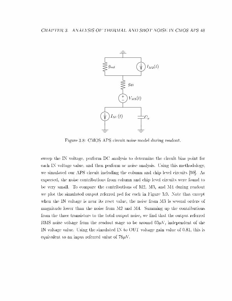
CHAPTER 3. ANALYSIS OF THERMAL AND SHOT NOISE IN CMOS APS 48
gd3
VM3(t)
gm2 IM2(t)
CoIM4(t)
Figure 3.8: CMOS APS circuit noise model during readout.
sweep the IN voltage, perform DC analysis to determine the circuit bias point for
each IN voltage value, and then perform ac noise analysis. Using this methodology,
we simulated our APS circuit including the column and chip level circuits [59]. As
expected, the noise contributions from column and chip level circuits were found to
be very small. To compare the contributions of M2, M3, and M4 during readout
we plot the simulated output referred psd for each in Figure 3.9. Note that except
when the IN voltage is near its reset value, the noise from M3 is several orders of
magnitude lower than the noise from M2 and M4. Summing up the contributions
from the three transistors to the total output noise, we �nd that the output referred
RMS noise voltage from the readout stage to be around 63�V, independent of the
IN voltage value. Using the simulated IN to OUT voltage gain value of 0:81, this is
equivalent to an input referred value of 78�V.
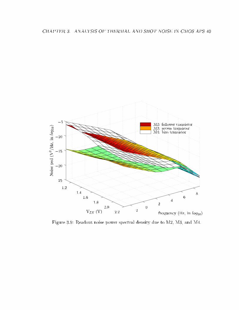
CHAPTER 3. ANALYSIS OF THERMAL AND SHOT NOISE IN CMOS APS 49
VIN (V) frequency (Hz, in log10)
Noisepsd(V2/Hz,inlog10) M2: follower transistor
M3: access transistorM4: bias transistor
�5
�10
�15
�20
�25
1:2
1:4
1:6
1:8
2:0
2:2 �20
24
68
Figure 3.9: Readout noise power spectral density due to M2, M3, and M4.
CHAPTER 3. ANALYSIS OF THERMAL AND SHOT NOISE IN CMOS APS 50
3.6 Summary
We presented a detailed and rigorous analysis of thermal and shot noise in CMOS
photodiode APS. We found that typical reset times are not long enough to achieve
steady state. Using time-domain analysis, we found that reset noise is very close
to kT
2C. This result, we believe, explains the discrepancy between measured reset
noise and the commonly quoted kT
Cvalue. We proposed a new pseudo- ash reset
method that alleviates image lag due to incomplete reset without increasing reset
noise. We analyzed noise due to the photodetector shot noise taking nonlinearity into
consideration and found that nonlinearity improves SNR at high illumination. For
completeness, we also analyzed noise during readout using both hand analysis and
SPICE simulation.
Chapter 4
Experiments
4.1 Introduction
Temporal noise is one of the most important parameters to measure when charac-
terizing CMOS image sensors. To measure temporal noise a number of other sensor
parameters must be determined �rst, including the sense node capacitance, readout
circuit conversion gain and linearity, etc. Once these parameters are known, some
other important image sensor characteristics, such as quantum eÆciency, spectral
response, and sensor array �xed pattern noise, can be readily estimated.
Techniques for characterizing CCD image sensors have been well established,
which is excellently described by Janesick in [25]. In that paper the CCD trans-
fer concept is introduced and used to characterize such parameters as charge transfer
eÆciency, quantum eÆciency, linearity, gain, o�set, signal to noise ratio, nonuniformi-
ty, dynamic range, and MTF. However, since the signal path for CMOS image sensors
is quite di�erent from CCDs, the CCD characterization models and techniques cannot
be directly used for characterizing a CMOS image sensor. For example, in a typical
CCD sensor all pixels share the same output ampli�er, and thus the output voltage
can be expressed as a linear function of the photogenerated charge plus shot noise
and readout noise, assuming constant gain across the pixels. As a result, di�erences
between pixel responses are primarily due to di�erences in their photodetector char-
acteristics, which are usually very small. By comparison, the output response for a
51
CHAPTER 4. EXPERIMENTS 52
CMOS APS can exhibit signi�cant nonlinearity[14], and pixel to pixel gain and o�-
set variations, due to the presence of the column and pixel ampli�ers which are not
shared by all pixels[32].
In this chapter, we describe the method to characterize CMOS APS. Similar to
Janesick's photon transfer method, we rely on the Poisson statistics of shot noise to
estimate the sense node capacitance, and thus the conversion gain. The di�erence
is that here we take into consideration the CMOS APS output response nonlinear-
ity, pixel to pixel gain and o�set variations, and readout noise. Using this method
we measure the capacitance, conversion gain, linearity, o�set, quantum eÆciency,
spectral response, �xed pattern noise, and temporal noise, for the test structures fab-
ricated in 0.35� standard CMOS processes. We �nd that the measured reset noise
mean square value is indeed close to kT
2C, as derived in chapter 3. The measured SNR
value also matches well with our analysis. We also demonstrate the incomplete reset
induced image lag.
The remainder of the chapter is organized as follows. In Section 4.2 we describe the
experiment setup, and the procedure we used to characterize CMOS image sensors.
In section 4.3, we present our experimental results of temporal noise in the CMOS
APS test structures.
4.2 Experiment Setup and Procedure
The experiment setup for characterizing CMOS APS sensors is shown in Figure 4.1.
The optical part of the setup consists of a DC regulated tungsten halogen light
source, a monochromator, an integrating sphere, and a calibrated photodiode. The
monochromator is controlled by a PC. The output of the integrating sphere is used to
provide the needed uniform illumination to the image sensor. The electrical part of
the setup consists of a pattern generator, a logical analyzer, highly regulated power
supply, and a device under test (DUT) board. The DUT board holds the test struc-
ture sensor chip, a low noise ampli�er, an analog to digital converter, some analog
bias circuits, and digital control signal interface. All of the electrical equipments and
the monochromator are GPIB programmable.
CHAPTER 4. EXPERIMENTS 53
A similar setup has been used to characterize digital pixel CMOS image sensors.
To test DPS, the optical part of the setup described in previous paragraph can be
kept the same, while the electrical part needs some modi�cation. In this case, the
pattern generator is replaced by a �eld programmable gate array (FPGA) board, and
the logical analyzer is replaced by an image capture board.
To accurately measure the sensor parameters, special care has been taken to min-
imize the environmental interference such as light source uctuations, temperature
uctuations, electromagnetic interference, etc. We housed the setup in a well air con-
ditioned dark room. We used a light source with intensity uctuations of less than
0:5%. The ripple of the dc power supply was limited to be less than 0:2%. Tem-
perature and light intensity were recorded each time data was taken. We remotely
performed all the experiments to minimize the human interference.
The analog sensor output is ampli�ed using the on board low noise ampli�er and
then quantized using an on board 16-bit ADC. The digital number is then collected
by a logical analyzer, and �nally transfered to a computer. All the critical analog
signals are coaxed to shield the environmental interference.
To measure the sense node capacitance, and hence the conversion gain, the sensor
is irradiated by a monochromatic light source through the integrating sphere. In the
measurements, instead of varying illumination (common in CCD methods), illumi-
nation is kept constant and the pixel output is continuously observed and sampled
at regular time intervals during integration time. Using this method the e�ect of
ampli�er o�sets can be eliminated, and the nonlinearity of the sensor response can
be approximated by a piecewise linear response. The experiment is repeated multiple
times to obtain good estimates of the pixel output mean and variance at each sample
time. The sensor response is approximated by a piecewise linear function. Using the
Poisson statistics of shot noise, which is also used in the CCD method, the system
conversion gain, collected charge, and read noise are estimated for each line segment.
This procedure is repeated at no illumination so that dark current generated charge
may be estimated and subtracted from the total charge estimates.
Now we describe the method quantitatively. Let N be the number of the indepen-
dent experiments we performed. Each experiment started with reseting the sensor,
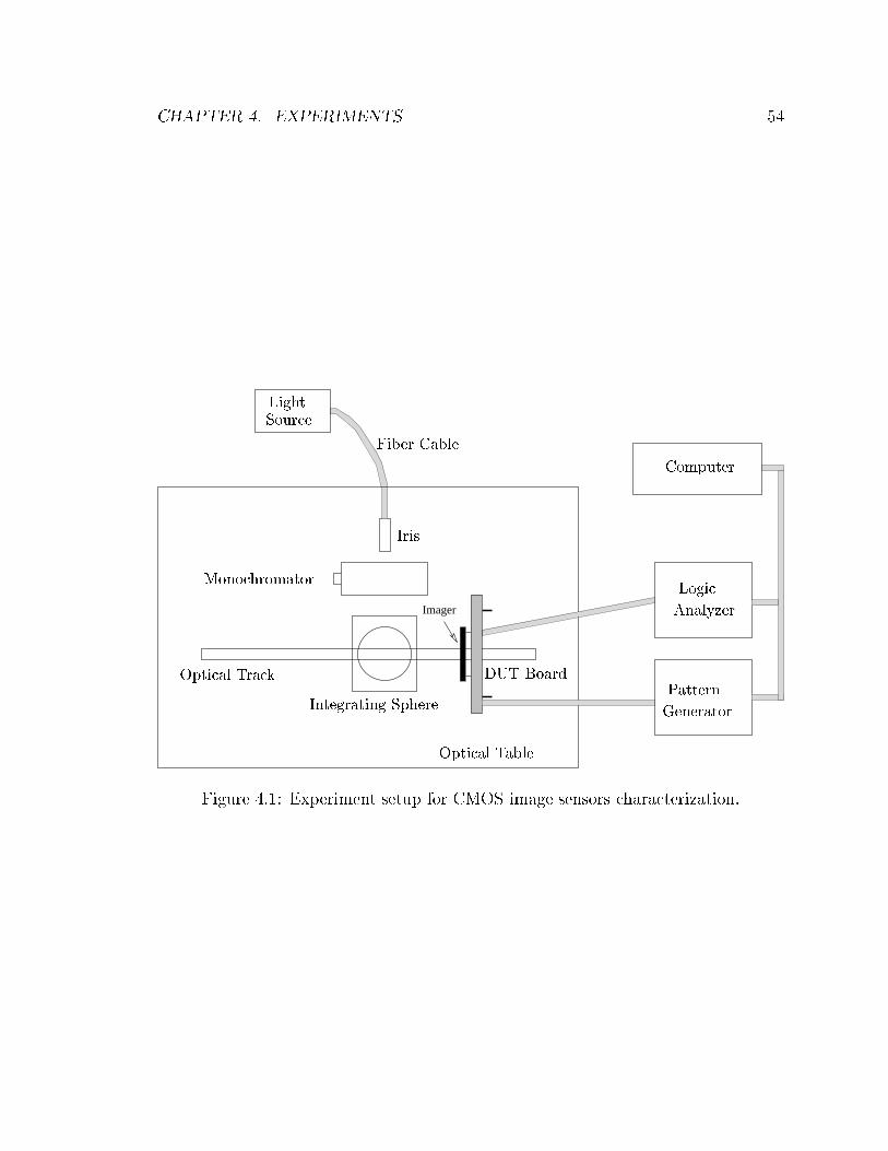
CHAPTER 4. EXPERIMENTS 54
Imager
LightSource
Logic
Analyzer
Computer
Integrating Sphere
Optical Table
Optical Track DUT BoardPattern
Generator
Iris
Monochromator
Fiber Cable
Figure 4.1: Experiment setup for CMOS image sensors characterization.
CHAPTER 4. EXPERIMENTS 55
and then contiously sampled the pixel output. Let M be the samples we took in
each experiment. We denote the samples by Vi;j, i = 1; : : : ; N and j = 1; : : : ;M . We
approximate the nonlinear sensor response using a piecewise linear model consisting
of K � 1 segments. For each set of voltage output samples Vi;j, j = 1; : : : ;M , the
�rst segment ranges from j = j0 = 1 to j1, the second from j = j1 to j2, and the last
from jK�1 to jK =M . The number of segments K is determined as follows. We �rst
investigate several output sample paths, and then choose a K which is large enough
to provide a good �t, but small enough that the number of samples per segment is
suÆcient for data analysis. The pixel output within segment s, 0 � s � K � 1 is
given by:
Vi;j = gsQi;j + Us;i + Zi;j; (4.1)
where gs is the conversion gain from the pixel to the sensor output for segment s
measured in volts/electron, Qi;j is the total charge (in electrons) collected at the jth
sample time (of path i), Us;i is the o�set of path i in segment s and is assumed to be
random with unknown mean and variance. The charge Qi;j is the sum of the photo-
generated charge Ql
i;jand leakage or dark charge Qd
i;j. Zi;j is the readout noise which
is assumed to be independent and identically distributed for all i and j, with zero
mean and unknown variance �2Z. The readout noise is also assumed to be independent
of the charge samples Qi;j, and the o�sets Us;i. Note that the gain gs can vary from
pixel to pixel. The following discussion will consider the output from a �xed pixel.
After the measurements and analysis are repeated for all pixels in the image sensors,
we can further estimate the gain and o�set �xed pattern noise.
To eliminate the o�set we normalize with respect to the �rst sample in each
segment to get that
Xs;i;(j�js) = gs(Qi;j �Qi;js) + Zi;j � Zi;js
; (4.2)
where j = js + 1; : : : ; js+1.
The charge increments Qi;j � Qi;jsare samples from a Poisson process and thus
CHAPTER 4. EXPERIMENTS 56
are Poisson random variables with mean and variance equal to
�l(j � js)� + �d(j � js)�;
where �l is the average photocurrent, �d is the average dark current, and � is time
interval between two consecutive samples. Thus, the mean and variance of the sample
Xs;i;(j�js) are given by:
E[Xs;i;(j�js)] = gs(�l + �d)(j � js)�; (4.3)
and
V ar[Xs;i;(j�js)] = g2s(�l + �d)(j � js)� + 2�2
Z; (4.4)
respectively.
Note that the sample means and variances can be estimated using
Xs;j =1
N
NXi=1
Xs;i;j; and (4.5)
�2s;j
=1
N � 1
NXi=1
�X2s;i;j
�Xs;j
2�; (4.6)
where j = 1; : : : ; js+1 � js.
The charge collected in segment s is then estimated as
Qls=
�gs(�l + �d)�
�2�g2s(�l + �d)�
� (js+1 � js): (4.7)
The same set of measurements and analysis is repeated under dark condition to obtain
an estimate of the dark charge in segment s
Qds=
�gs(�d)�
�2�g2s(�d)�
� (js+1 � js): (4.8)
Now let Xp
s;(js+1�js)be the mean output value of pixel p in segment s at the last
CHAPTER 4. EXPERIMENTS 57
sample (js+1 � js), then
gps =
TXp
s;(js+1�js)
(js+1 � js)�P
K�1s=0 (Q
ls�Qd
s); (4.9)
where T is the total integration time.
Once conversion gain is determined, we can measure the sensor �xed pattern
noise (FPN) and quantum eÆciency (QE). FPN measurements involve irradiating
the sensor with uniform light and analyzing the intensity variations of the supposedly
uniform output images. Uniform irradiation is achieved by �rst shining the light
source into an integrating sphere. The uniform light emitted from the exit port of
the integrating sphere is then used to irradiate the sensor.
QE is the fraction of photon ux that contributes to the photocurrent in a pho-
todetector or in a pixel. To measure QE, the photon ux incident on the sensor must
be determined. The experiment setup is almost identical to that of FPN measure-
ments. The only additional step here is that, after collecting measurements with the
chip, the sensor chip is moved aside and a calibrated photodiode is placed at the same
position as the sensor chip, to measure incident light intensity. The spectral response
curve of the image sensor can be obtained by the procedure used to estimate QE. We
only need to illuminate the sensor with a monochromatic light source placed in front
of the integrating sphere and estimate QE at each wavelength of light. Note that in
FPN, QE, and spectral response measurements, the experiments must be repeated
many times under the same condition, to remove the temporal noise.
To measure the temporal noise, we only pick a group of representative pixels that
have normal QE and spectral response. The output value of these pixels must be close
to the average output value of all pixels when the sensor is irradiated with uniform
light. By doing so, we can reduce the amount of data to be processed, and can
increase the measurement accuracy. The experiment is again repeated many times
under the same condition, and the temporal noise is calculated using the variance
estimator. The requirement of removing environmental interference is most strict in
noise measurements, because the interference can often overwhelm the \true" noise
one intended to measure.
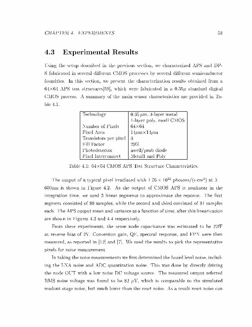
CHAPTER 4. EXPERIMENTS 58
4.3 Experimental Results
Using the setup described in the previous section, we characterized APS and DP-
S fabricated in several di�erent CMOS processes by several di�erent semiconductor
foundries. In this section, we present the characterization results obtained from a
64�64 APS test structures[59], which were fabricated in a 0.35� standard digital
CMOS process. A summary of the main sensor characteristics are provided in Ta-
ble 4.1.
Technology 0.35�m, 4-layer metal
1-layer poly, nwell CMOS
Number of Pixels 64�64
Pixel Area 14�m�14�m
Transistors per pixel 3
Fill Factor 29%
Photodetector nwell/psub diode
Pixel Interconnect Metal1 and Poly
Table 4.1: 64�64 CMOS APS Test Structure Characteristics.
The output of a typical pixel irradiated with 1:76� 1012 photons/(s�cm2) at � =
600nm is shown in Figure 4.2. As the output of CMOS APS is nonlinear in the
integration time, we used 3 linear segments to approximate the reponse. The �rst
segment consisted of 80 samples, while the second and third consisted of 81 samples
each. The APS output mean and variance as a function of time, after this linearization
are shown in Figures 4.3 and 4.4 respectively.
From these experiments, the sense node capacitance was estimated to be 22fF
at reverse bias of 2V. Conversion gain, QE, spectral response, and FPN were then
measured, as reported in [12] and [7]. We used the results to pick the representative
pixels for noise measurement
In taking the noise measurements we �rst determined the board level noise, includ-
ing the LNA noise and ADC quantization noise. This was done by directly driving
the node OUT with a low noise DC voltage source. The measured output referred
RMS noise voltage was found to be 82 �V, which is comparable to the simulated
readout stage noise, but much lower than the reset noise. As a result reset noise can
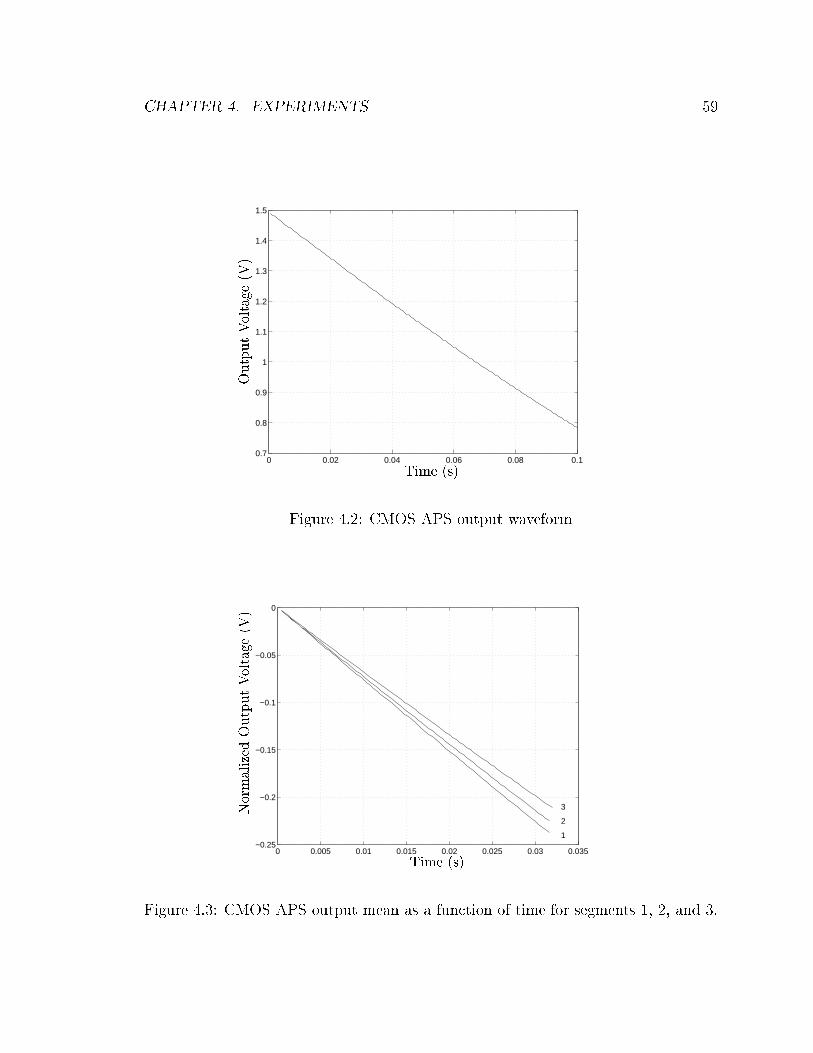
CHAPTER 4. EXPERIMENTS 59
0 0.02 0.04 0.06 0.08 0.10.7
0.8
0.9
1
1.1
1.2
1.3
1.4
1.5
Time (s)
OutputVoltage(V)
Figure 4.2: CMOS APS output waveform
0 0.005 0.01 0.015 0.02 0.025 0.03 0.035−0.25
−0.2
−0.15
−0.1
−0.05
0
3
2
1
NormalizedOutputVoltage(V)
Time (s)
Figure 4.3: CMOS APS output mean as a function of time for segments 1, 2, and 3.
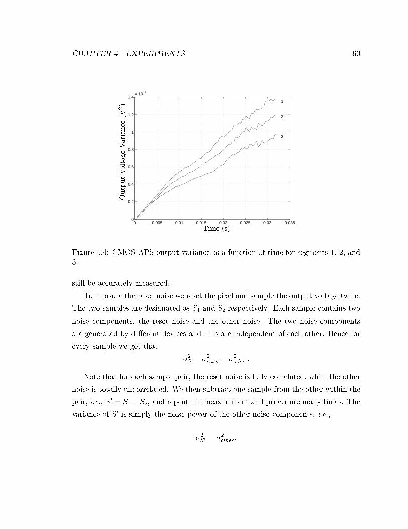
CHAPTER 4. EXPERIMENTS 60
0 0.005 0.01 0.015 0.02 0.025 0.03 0.0350
0.2
0.4
0.6
0.8
1
1.2
1.4x 10
−6
1
2
3
Time (s)
OutputVoltageVariance(V2)
Figure 4.4: CMOS APS output variance as a function of time for segments 1, 2, and
3.
still be accurately measured.
To measure the reset noise we reset the pixel and sample the output voltage twice.
The two samples are designated as S1 and S2 respectively. Each sample contains two
noise components, the reset noise and the other noise. The two noise components
are generated by di�erent devices and thus are independent of each other. Hence for
every sample we get that
�2S= �2
reset+ �2
other:
Note that for each sample pair, the reset noise is fully correlated, while the other
noise is totally uncorrelated. We then subtract one sample from the other within the
pair, i.e., S 0 = S1�S2, and repeat the measurement and procedure many times. The
variance of S 0 is simply the noise power of the other noise components, i.e.,
�2S0= �2
other:
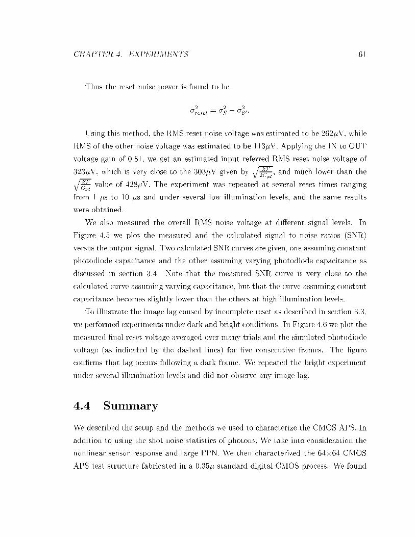
CHAPTER 4. EXPERIMENTS 61
Thus the reset noise power is found to be
�2reset
= �2S� �2
S0:
Using this method, the RMS reset noise voltage was estimated to be 262�V, while
RMS of the other noise voltage was estimated to be 113�V. Applying the IN to OUT
voltage gain of 0:81, we get an estimated input referred RMS reset noise voltage of
323�V, which is very close to the 303�V given byq
kT
2Cpd, and much lower than theq
kT
Cpdvalue of 428�V. The experiment was repeated at several reset times ranging
from 1 �s to 10 �s and under several low illumination levels, and the same results
were obtained.
We also measured the overall RMS noise voltage at di�erent signal levels. In
Figure 4.5 we plot the measured and the calculated signal to noise ratios (SNR)
versus the output signal. Two calculated SNR curves are given, one assuming constant
photodiode capacitance and the other assuming varying photodiode capacitance as
discussed in section 3.4. Note that the measured SNR curve is very close to the
calculated curve assuming varying capacitance, but that the curve assuming constant
capacitance becomes slightly lower than the others at high illumination levels.
To illustrate the image lag caused by incomplete reset as described in section 3.3,
we performed experiments under dark and bright conditions. In Figure 4.6 we plot the
measured �nal reset voltage averaged over many trials and the simulated photodiode
voltage (as indicated by the dashed lines) for �ve consecutive frames. The �gure
con�rms that lag occurs following a dark frame. We repeated the bright experiment
under several illumination levels and did not observe any image lag.
4.4 Summary
We described the setup and the methods we used to characterize the CMOS APS. In
addition to using the shot noise statistics of photons, We take into consideration the
nonlinear sensor response and large FPN. We then characterized the 64�64 CMOS
APS test structure fabricated in a 0.35� standard digital CMOS process. We found
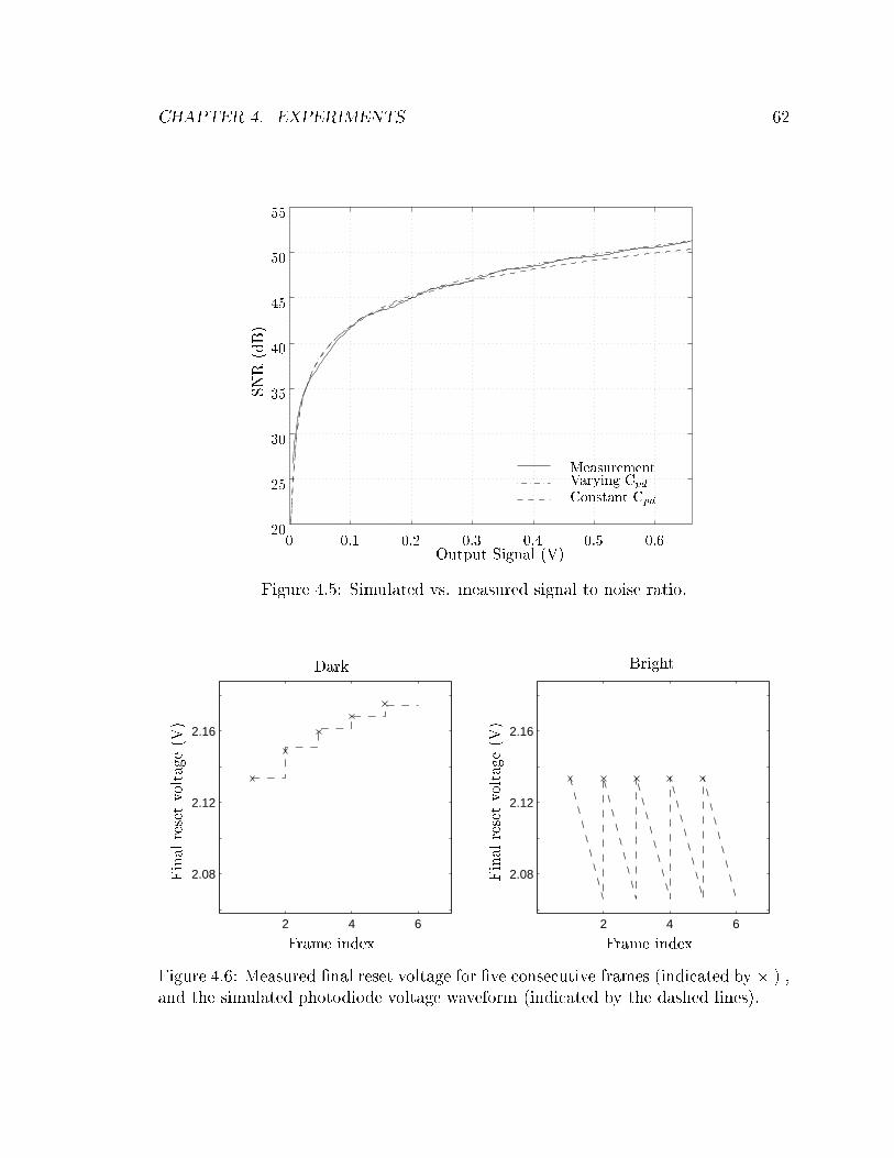
CHAPTER 4. EXPERIMENTS 62
55
50
45
40
35
30
25
200 0.1 0.2 0.3 0.4 0.5 0.6
SNR(dB)
Output Signal (V)
MeasurementVarying CpdConstant Cpd
Figure 4.5: Simulated vs. measured signal to noise ratio.
2 4 6
2.08
2.12
2.16
2 4 6
2.08
2.12
2.16
Dark Bright
Frame indexFrame index
Finalresetvoltage(V)
Finalresetvoltage(V)
Figure 4.6: Measured �nal reset voltage for �ve consecutive frames (indicated by � ) ,
and the simulated photodiode voltage waveform (indicated by the dashed lines).
CHAPTER 4. EXPERIMENTS 63
that the measured reset noise is indeed very close to the half kT/C result derived in
previous chapter. The measured SNR is also consistent to the calculated shot noise
using the nonlinear model we developed in previous chapter.
Chapter 5
MOSFET 1/f Noise Models
5.1 Introduction
The analysis of 1/f noise in CMOS APS is typically performed in frequency domain,
using the standard 1/f noise model. A low cuto� frequency is typically used to get
reasonable noise power estimates. The choice of this low cuto� frequency is quite
arbitrary, however, and can cause signi�cant inaccuracy in estimating noise power.
So in this chapter, we start from the �rst principles to derive a 1/f noise model that
is more suitable for analyzing 1/f noise in CMOS APS.
Historically, 1/f noise in MOSFETs has been of concern mainly in the design of
low frequency linear analog circuits such as bias circuits, audio ampli�ers, etc. [16].
As CMOS technology scaled down to the submicron regime, 1/f noise has become of
greater concern in a wider range of circuit designs. Scaling has enabled the use of
CMOS technology in many new applications such as RF circuits and CMOS image
sensors that are quite sensitive to 1/f noise. Moreover, as mentioned in [20] 1/f noise
in MOSFETs increases rapidly with technology scaling. As a result it is becoming
more important to be able to accurately estimate the e�ect of 1/f noise for a wide
variety of circuits.
Analysis of 1/f noise in MOSFET circuits is typically performed using the well
established stationary 1/f noise model [22, 24], which henceforth will be referred to as
the standard 1/f noise model. Recent experimental results, however, show that the
64
CHAPTER 5. MOSFET 1/F NOISE MODELS 65
estimates using this standard model can be quite inaccurate especially for switched
circuits. An important class of such circuits is the periodically switched circuits, which
are widely used in RF applications, such as switched capacitor networks, modulators
and demodulators, and frequency converters. In the simplest case of such circuits,
which involves only a periodically switched transistor, it was shown that the measured
drain voltage 1/f noise psd [1, 6, 15] is much lower than the estimates using the
standard 1/f noise model. Another example that has recently been receiving much
attention is 1/f-induced phase noise in CMOS oscillators [18, 17, 40]. Unlike the
amplitude uctuations, which can be practically eliminated by applying limiters to
the output signal, phase noise cannot be reduced in the same manner. As a result,
it limits the available channel in wireless communication. Recent measurements [15]
show that the 1/f-induced phase noise power spectral density (psd) in ring oscillators
is much lower than the estimate using the standard 1/f noise model.
In this chapter, we propose a nonstationary extension of the standard 1/f noise
model, which accurately models 1/f noise when the transistor is switched from the
o� to the on state. The model is based on the fact that when the MOSFET is
o� the active traps are mostly empty. By modifying the random telegraph signal
(RTS) model for a single trap to re ect this fact, the noise autocovariance function
is derived. We will then show that this nonstationary model can be used to obtain
accurate estimates of the e�ect of 1/f noise in switched circuits. In particular we
consider the aforementioned example circuits.
The rest of the chapter is organized as follows. In section 5.2 we review the
standard 1/f noise model. In section 5.3 we present our nonstationary extension. In
sections 5.4 and 5.5 we use our nonstationary model to estimate the e�ect of 1/f noise
on a periodically switched transistor, and ring oscillator, respectively. In both cases
we �nd that our estimates are consistent with the reported measurement results.
5.2 Standard 1/f Noise Model
1/f noise (sometimes also called icker noise, or low frequency noise), in the strictest
sense, refers to the noise whose power spectral density (psd) is inversely proportional
CHAPTER 5. MOSFET 1/F NOISE MODELS 66
to frequency, i.e., SN /1jf j. More generally, noise with SN /
1jf j�
, for � > 0, is also
called 1/f noise (or 1/f like noise). In addition to electronic devices, 1/f noise also
appears in many other devices and natural phenomena, such as oscillation of quartz
crystals, geophysical records, economic data, traÆc- ow rates, image texture, heart
beat rates, : : :, just to name a few. As a result, the origin of 1/f noise has been the
subject of numerous studies in many di�erent �elds. Unfortunately, since 1/f psd is
not integrable, it is not a valid psd of stationary processes and there is no agreed
upon universal mathematical or physical model to describe it.
In this thesis we are mainly concerned with 1/f noise in MOS transistors. Over the
last three decades, two main theories of 1/f noise in MOS transistors were developed,
namely the carrier number uctuation theory, and the mobility uctuation theory [54].
The carrier number uctuation theory attributes 1/f noise to random capture and
emission of conduction channel carriers by traps in the gate oxide, while the mobility
uctuation theory considers the 1/f noise as a result of the uctuation in the carrier
mobility. Both theories succeeded in partially explaining some of the experimental
data. However, since it was very diÆcult to experimentally verify the noise generation
mechanism, there was no conclusive evidence to support either theory.
This controversy has, to a large extent, been resolved by recent studies of small
area sub-micron MOS transistors. In these transistors, very few, (sometimes only
one) traps are active in the gate oxide. Capture and emission of channel carriers by
this trap are represented by the trapped electron number N(t), which takes the value
1 if a carrier is captured and zero otherwise, as depicted in Figure 5.1. The trap is
active when its energy level is close to the Fermi level [28] in the bulk. In this case
the capture and emission rates must be nearly equal. Thus, N(t) can be modeled as
a Random Telegraph Signal (RTS) with rate �. In equilibrium, the autocovariance
of N(t) is given by
C�(�) =1
4e�2�� ;
and the corresponding double sided power spectral density (psd) is
S�(f) =1
4
�
�2 + (�f)2:
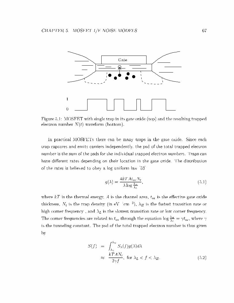
CHAPTER 5. MOSFET 1/F NOISE MODELS 67
Gate
1
0
Figure 5.1: MOSFET with single trap in its gate oxide (top) and the resulting trapped
electron number N(t) waveform (bottom).
In practical MOSFETs there can be many traps in the gate oxide. Since each
trap captures and emits carriers independently, the psd of the total trapped electron
number is the sum of the psds for the individual trapped electron numbers. Traps can
have di�erent rates depending on their location in the gate oxide. The distribution
of the rates is believed to obey a log uniform law [53]
g(�) =4kTAtoxNt
� log �H
�L
; (5.1)
where kT is the thermal energy, A is the channel area, tox is the e�ective gate oxide
thickness, Nt is the trap density (in eV�1cm�3), �H is the fastest transition rate or
high corner frequency , and �L is the slowest transition rate or low corner frequency.
The corner frequencies are related to tox through the equation log�H
�L= tox, where
is the tunneling constant. The psd of the total trapped electron number is thus given
by
S(f) =
Z�H
�L
S�(f)g(�)d�
�kTANt
2 f; for �L < f < �H : (5.2)
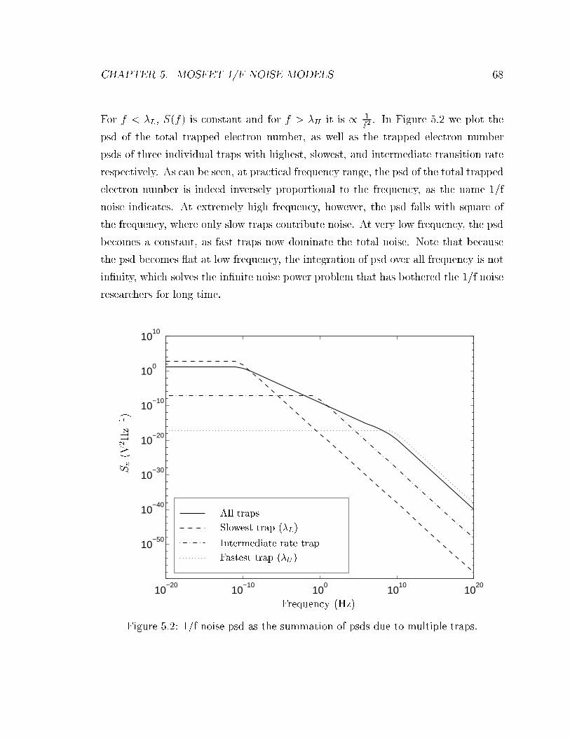
CHAPTER 5. MOSFET 1/F NOISE MODELS 68
For f < �L, S(f) is constant and for f > �H it is / 1f2. In Figure 5.2 we plot the
psd of the total trapped electron number, as well as the trapped electron number
psds of three individual traps with highest, slowest, and intermediate transition rate
respectively. As can be seen, at practical frequency range, the psd of the total trapped
electron number is indeed inversely proportional to the frequency, as the name 1/f
noise indicates. At extremely high frequency, however, the psd falls with square of
the frequency, where only slow traps contribute noise. At very low frequency, the psd
becomes a constant, as fast traps now dominate the total noise. Note that because
the psd becomes at at low frequency, the integration of psd over all frequency is not
in�nity, which solves the in�nite noise power problem that has bothered the 1/f noise
researchers for long time.
10−20
10−10
100
1010
1020
10−50
10−40
10−30
10−20
10−10
100
1010
Frequency (Hz)
Sv
(V2Hz�1)
All traps
Slowest trap (�L)
Intermediate rate trap
Fastest trap (�U )
Figure 5.2: 1/f noise psd as the summation of psds due to multiple traps.
CHAPTER 5. MOSFET 1/F NOISE MODELS 69
The MOSFET charge-control analysis can then be used together with the derived
psd of the total trapped electron number to �nd the 1/f noise psd of the drain current.
For submicron n-channel MOSFET, carrier number uctuations dominate [4, 2] and
the equivalent 1/f noise psd of the drain current is given by
SId(f) = g2mSVg(f) = g2
m
1
C2ox
SQch(f) = g2
m
1
C2ox
(q
A)2S(f) =
g2mq2kTNt
2C2oxA f
; (5.3)
where Cox is the gate oxide capacitance, gm is the transconductance, SVg(f) is the
equivalent gate voltage 1/f noise psd, and SQch(f) is the channel charge density 1/f
noise psd. Note that SId(f) is inversely proportional to the gate area, which explains
the reason why 1/f noise is becoming more pronounced as technology scales.
Circuit designers typically use the SPICE 1/f noise model
SVg(f) =kF
2CoxAf;
and are given the value of the SPICE 1/f noise parameter kF . From equation 5.3, we
�nd that
kF =q2kTNt
Cox :
A uni�ed number and mobility theory [22] can be used to extend these results to
p-channel MOSFETs.
5.3 Nonstationary 1/f Noise Model
In this section, we present our nonstationary extension of the standard 1/f noise model
discussed in the previous section. The main purpose of the extension is to be able to
more accurately analyze 1/f noise in switched circuits. We begin by considering the
case of a single trap in an n-channel MOSFET. The key observation that led to our
extension is that with very high probability the trap is empty when the transistor is
o�. The physical reason can be explained via the MOSFET energy band diagram in
Figure 5.3. The energy levels Eo
tand Et represent the trap energy in the o� and on
states, respectively. Note that for the trap to be active when the transistor is on Et
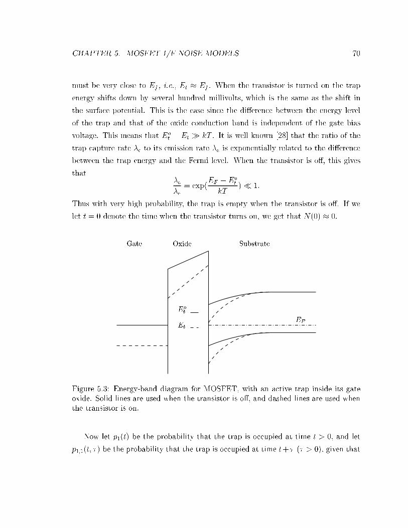
CHAPTER 5. MOSFET 1/F NOISE MODELS 70
must be very close to Ef , i.e., Et � Ef . When the transistor is turned on the trap
energy shifts down by several hundred millivolts, which is the same as the shift in
the surface potential. This is the case since the di�erence between the energy level
of the trap and that of the oxide conduction band is independent of the gate bias
voltage. This means that Eo
t� Et � kT . It is well known [28] that the ratio of the
trap capture rate �c to its emission rate �e is exponentially related to the di�erence
between the trap energy and the Fermi level. When the transistor is o�, this gives
that�c
�e= exp(
EF � Eo
t
kT)� 1:
Thus with very high probability, the trap is empty when the transistor is o�. If we
let t = 0 denote the time when the transistor turns on, we get that N(0) � 0.
Et
Eo
t
EF
SubstrateOxideGate
Figure 5.3: Energy-band diagram for MOSFET, with an active trap inside its gate
oxide. Solid lines are used when the transistor is o�, and dashed lines are used when
the transistor is on.
Now let p1(t) be the probability that the trap is occupied at time t > 0, and let
p1;1(t; �) be the probability that the trap is occupied at time t+ � (� > 0), given that
CHAPTER 5. MOSFET 1/F NOISE MODELS 71
it is occupied at time t. The autocovariance function of N(t) is then given by
C�(t; �) = p1(t)p1;1(�)� p1(t)p1(t+ �)
To �nd p1(t) we note that
p1(t+�t) = p1(t)(1� ��t) + (1� p1(t))��t: (5.4)
Thus in the limitdp1(t)
dt+ 2�p1(t) = �: (5.5)
Solving for p1 we get that
p1(t) =1
2(1� e�2�t): (5.6)
To �nd p1;1(t; �) we let p1;0(t; �) be the probability that the trap is empty at time
t+ � (� > 0), given that it is occupied at time t. Note that p1;0(t; �) = 1� p1;1(t; �),
and that
p1;1(t+ � +��) = p1;1(t; �)(1� ���) + p1;0(t; �)���: (5.7)
Thus in the limitdp1;1(t; �)
d�+ 2�p1;1(t; �) = �: (5.8)
Solving for p1;1 we get that
p1;1(t; �) = p1;1(�) =1
2(1 + e�2�� ): (5.9)
Therefore the autocovariance function of N(t) is given by
C�(t; �) = p1(t)p1;1(�)� p1(t)p1(t+ �)
=1
4e�2�� (1� e�4�t): (5.10)
As t!1, C�(t; �)!14e�2�� , which is the stationary autocovariance function derived
in the previous section.
The autocovariance of the total trapped electron number is simply the sum of the
CHAPTER 5. MOSFET 1/F NOISE MODELS 72
autocovariances for the individual traps in the gate oxide, i.e.,
C(t; �) =
Z�H
�L
C�(t; �)g(�)d�:
Applying charge-control analysis, we get the resulted mean square gate voltage as
V 2g(t) = (
q
ACox
)2Z�H
�L
C�(t; 0)g(�)d�: (5.11)
This integral does not have a closed form solution, and must be evaluated numer-
ically.
We now compare the 1/f noise power computed using the conventional frequency
domain method to the more accurate time domain method described. For the com-
parison and for the remainder of the thesis we assume a 0:35�m CMOS technology
with tox = 7nm, = 108cm�1, �H = 1010s�1, and Nt = 1017eV�1cm�3. Using these
parameter values we get �L = 4� 10�21, Cox = 5fF�m�2, and kF = 5� 10�24V2F at
T = 300K.
In Figure 5.4, we plot the RMS gate voltageqV 2gdue to the 1/f noise as a function
of the circuit on-time ton using both the standard model and our nonstationary ex-
tension. Shown in the bottom half of the �gure is the error using the standard model
as a percentage, referred to the result using the nonstationary model. As expected
the error percentage decreases as ton increases. In this example, we assume that the
channel area A = 1�m2.
5.4 1/f Noise in a Periodically Switched Transistor
Periodically switched circuits are widely used in RF applications, such as switched
capacitor networks, modulators and demodulators, and frequency converters. Un-
like linear circuitry, these circuits typically undergo large signal periodic variations in
their operation and thus are often modeled as linear periodically time varying (LPTV)
systems. As well known, a linear time varying system can be completely described
by the time varying impulse response h(t; �). However, in order to fully exploit the
periodicity and to contribute to design insight, LPTV systems are usually analyzed
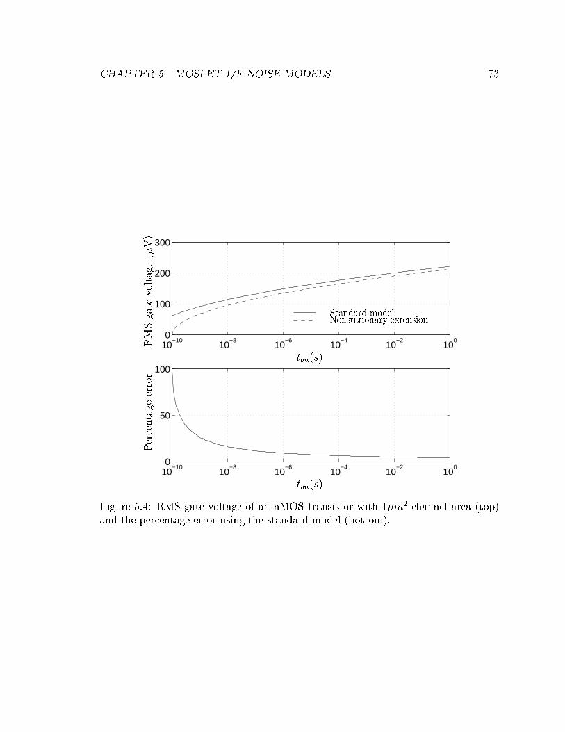
CHAPTER 5. MOSFET 1/F NOISE MODELS 73
10−10
10−8
10−6
10−4
10−2
100
0
100
200
300
10−10
10−8
10−6
10−4
10−2
100
0
50
100
ton(s)
ton(s)
Percentageerror
RMSgatevoltage(�V)
Standard modelNonstationary extension
Figure 5.4: RMS gate voltage of an nMOS transistor with 1�m2 channel area (top)
and the percentage error using the standard model (bottom).
CHAPTER 5. MOSFET 1/F NOISE MODELS 74
in frequency domain. According to the generalized Wiener-Khintchine theorem [29],
Fourier transform of h(t; �) with regards to � results in the periodically time vary-
ing system transfer function H(t; f). H(t; f) is then expanded using Fourier series
representation, leading to the harmonic transfer functions [47]. Using this approach,
It becomes obvious that an input signal at certain frequency could cause an output
signal that have di�erent frequency content, which is in contrary to the behavior of
linear time invariant circuits. The statistics of noise in periodically switched circuits
is also vary periodically in time, leading to certain important e�ects such as up and
down conversion of noise spectra. A good such example is given in [41], dealing with
time varying shot noise.
In this section we use our nonstationary 1/f noise model to analyze the simplest
example of such circuits, a periodically switched transistor. Figure 5.5 depicts a
typical setup for measuring 1/f noise psd for a transistor. In the periodically switched
case the gate of the transistor is driven by a square wave voltage source that switched
between 0V and vH , which is high enough to bias the transistor in the saturation
region. Measured 1/f noise psd using this setup was reported in [1, 6, 15]. These
papers comment on the fact that the measured psd is signi�cantly lower than the psd
estimated using the standard 1/f model. We now show that our nonstationary model
can be used to obtain results that are more consistent with these measurements.
We begin by considering a single active trap. To simplify the analysis, we assume
that when the transistor is o�, the trap is empty. Using equation 5.10, we can write
the autocovariance function of the trapped electron number as
C�(t; �) =
8<:
14e�2�� (1� e�4�(t�nT )) nT � t; t+ � � nT + T
2
0 otherwise(5.12)
Note that C�(t; �) is periodic in t, and that the trapped electron number is a wide
sense cyclostationary process. As proved in [47, 21, 41], low pass �ltering or band
pass �ltering of a wide sense cyclostationary process results in a wide sense stationary
process when the �lter bandwidth is less than half the switching frequency 1T. Spec-
trum analyzers normally perform this conversion before the spectrum is determined.
Therefore the autocovariance of the resulting stationary process can be obtained by
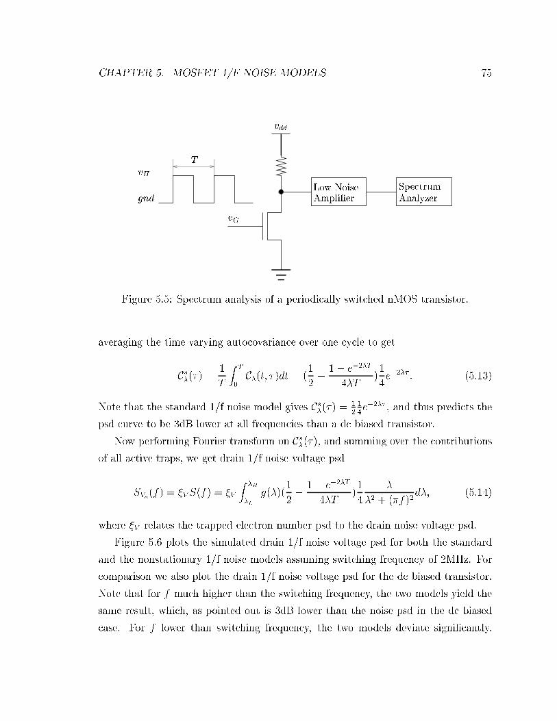
CHAPTER 5. MOSFET 1/F NOISE MODELS 75
vdd
vH
gnd
T
vG
Low NoiseAmpli�er
Spectrum
Analyzer
Figure 5.5: Spectrum analysis of a periodically switched nMOS transistor.
averaging the time varying autocovariance over one cycle to get
Cs
�(�) =
1
T
ZT
0C�(t; �)dt = (
1
2�1� e�2�T
4�T)1
4e�2�� : (5.13)
Note that the standard 1/f noise model gives Cs�(�) = 1
214e�2�� , and thus predicts the
psd curve to be 3dB lower at all frequencies than a dc biased transistor.
Now performing Fourier transform on Cs�(�), and summing over the contributions
of all active traps, we get drain 1/f noise voltage psd
SVd(f) = �V S(f) = �V
Z�H
�L
g(�)(1
2�1� e�2�T
4�T)1
4
�
�2 + (�f)2d�; (5.14)
where �V relates the trapped electron number psd to the drain noise voltage psd.
Figure 5.6 plots the simulated drain 1/f noise voltage psd for both the standard
and the nonstationary 1/f noise models assuming switching frequency of 2MHz. For
comparison we also plot the drain 1/f noise voltage psd for the dc biased transistor.
Note that for f much higher than the switching frequency, the two models yield the
same result, which, as pointed out is 3dB lower than the noise psd in the dc biased
case. For f lower than switching frequency, the two models deviate signi�cantly.
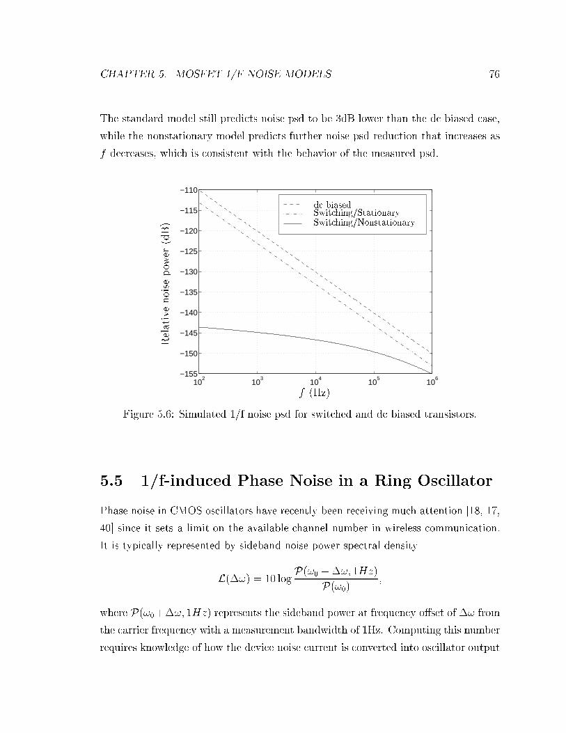
CHAPTER 5. MOSFET 1/F NOISE MODELS 76
The standard model still predicts noise psd to be 3dB lower than the dc biased case,
while the nonstationary model predicts further noise psd reduction that increases as
f decreases, which is consistent with the behavior of the measured psd.
102
103
104
105
106
−155
−150
−145
−140
−135
−130
−125
−120
−115
−110
f (Hz)
Relativenoisepower(dB) Switching/Nonstationary
Switching/Stationarydc biased
Figure 5.6: Simulated 1/f noise psd for switched and dc biased transistors.
5.5 1/f-induced Phase Noise in a Ring Oscillator
Phase noise in CMOS oscillators have recently been receiving much attention [18, 17,
40] since it sets a limit on the available channel number in wireless communication.
It is typically represented by sideband noise power spectral density
L(�!) = 10 logP(!0 +�!; 1Hz)
P(!0);
where P(!0+�!; 1Hz) represents the sideband power at frequency o�set of �! from
the carrier frequency with a measurement bandwidth of 1Hz. Computing this number
requires knowledge of how the device noise current is converted into oscillator output
CHAPTER 5. MOSFET 1/F NOISE MODELS 77
voltage. In [17] this is done in two steps. The �rst step involves the conversion of
excess injected current into excess phase, which is done via a linear time varying
system (LTVS). The second step is phase modulation, where the excess phase is
converted into voltage. The LTVS is characterized by its impulse response
h(t; �) =�(!0�)
qmaxu(t� �);
where qmax is the maximum charge displacement, u is the unit step function, and �
is the periodic impulse sensitivity function (ISF). Expanding
�(!0�) =c0
2+
1Xn=1
cn cos(n!0� + �n);
and assuming excess injected current due to 1/f noise with psd �kF
CoxA�!, it can be
shown that
L(�!) = 10 log(c20�kF
4q2max
CoxA
1
�!3) (5.15)
Thus the low frequency noise power gets upconverted to the sideband noise power,
which is usually at very high frequency. Note that its power is falling as 1�!3
here.
This approach, however, cannot be used to explain the abnormal reduction in
phase noise when the transistors in a ring oscillator are periodically turned on and
o� [15]. We now show that using our nonstationary 1/f noise model, we can explain
this reduction. To simplify the derivation, we consider the case where one of the
transistors has a much smaller area than the others, and thus its 1/f-induced phase
noise dominates. To study the noise due to this transistor, we �rst consider the case
where there is only one active trap. Using the periodic autocovariance function of the
trapped electron number as expressed in equation 5.12, we can �nd the time varying
psd [29]
S(t; f) =
8<:
14
�
�2+(�f)2(1� e�4�(t�nT )) nT � t; t + � � nT + T
2
0 otherwise(5.16)
CHAPTER 5. MOSFET 1/F NOISE MODELS 78
Note that S(t; f) can be seperated as S(f)�(t), where S(f) = 14
�
�2+(�f)2and �(t)
is the remaining periodic function. For this class of cyclostationary noise sources, it
is shown [17] that phase noise can still be calculated using equation 5.15, with S(f)
representing the noise source, and c0 computed using �eff (t) = �(t)�(t) as the new
ISF. In [17] it is also shown that for independent noise sources the total phase noise is
simply the sum of the phase noise due to each source. We can use this fact to �nd the
1/f-induced phase noise psd in the case of many traps, since their trapped electron
numbers are independent.
To demonstrate that our nonstationary 1/f noise model can be used to explain the
reduction in phase noise consider a ring oscillator with the ISF shown in Figure 5.7.
The �gure also plots the gate voltage for the transistor under consideration. Figure 5.8
plots the simulated phase noise psd using both the nonstationary and the standard
1/f noise models at 2MHz switching frequency. We also plot the phase noise psd of
a non-switching ring oscillator, where the transistor is always on. As can be seen,
the standard 1/f noise model reports phase noise that is 6dBc lower than the non-
switching case, for all frequencies. The 6dBc reduction, however, is too small when
compared to the reported measurements [15], which show over 10dBc reduction in
the 1-10kHz range. By comparison, the plot using our nonstationary model shows
10-20dBc reduction in this frequency range. The reduction is caused by the decrease
in 1/f noise due to the switching of the transistor as discussed in the previous section.
Note that our model predicts an increase in 1/f-induced phase noise above 100kHz
relative to the estimates of the stationary model. This we believe is due to the non at
shape of the �(t) as shown in Figure 5.7, which can cause signi�cant asymmetry in
the e�ective ISF, and thus can increase phase noise.
5.6 Summary
We described a nonstationary extension to the standard 1/f noise model. The model is
based on the fact that the active traps are mostly empty when the MOSFET is o�. By
modifying the RTS model for a single trap to re ect this fact, the noise autocovariance
function can be numerically evaluated. We then used our nonstationary extension of
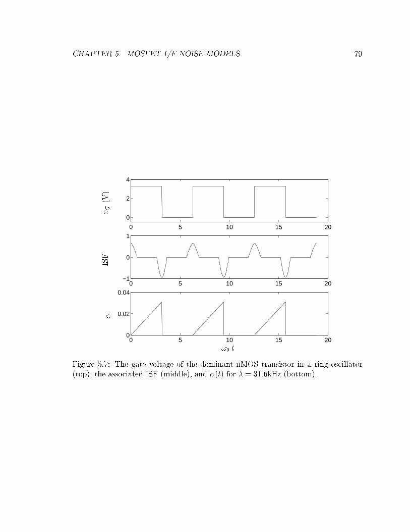
CHAPTER 5. MOSFET 1/F NOISE MODELS 79
0 5 10 15 20
0
2
4
0 5 10 15 20−1
0
1
0 5 10 15 200
0.02
0.04
!0 t
vG
(V)
ISF
�
Figure 5.7: The gate voltage of the dominant nMOS transistor in a ring oscillator
(top), the associated ISF (middle), and �(t) for � = 31:6kHz (bottom).
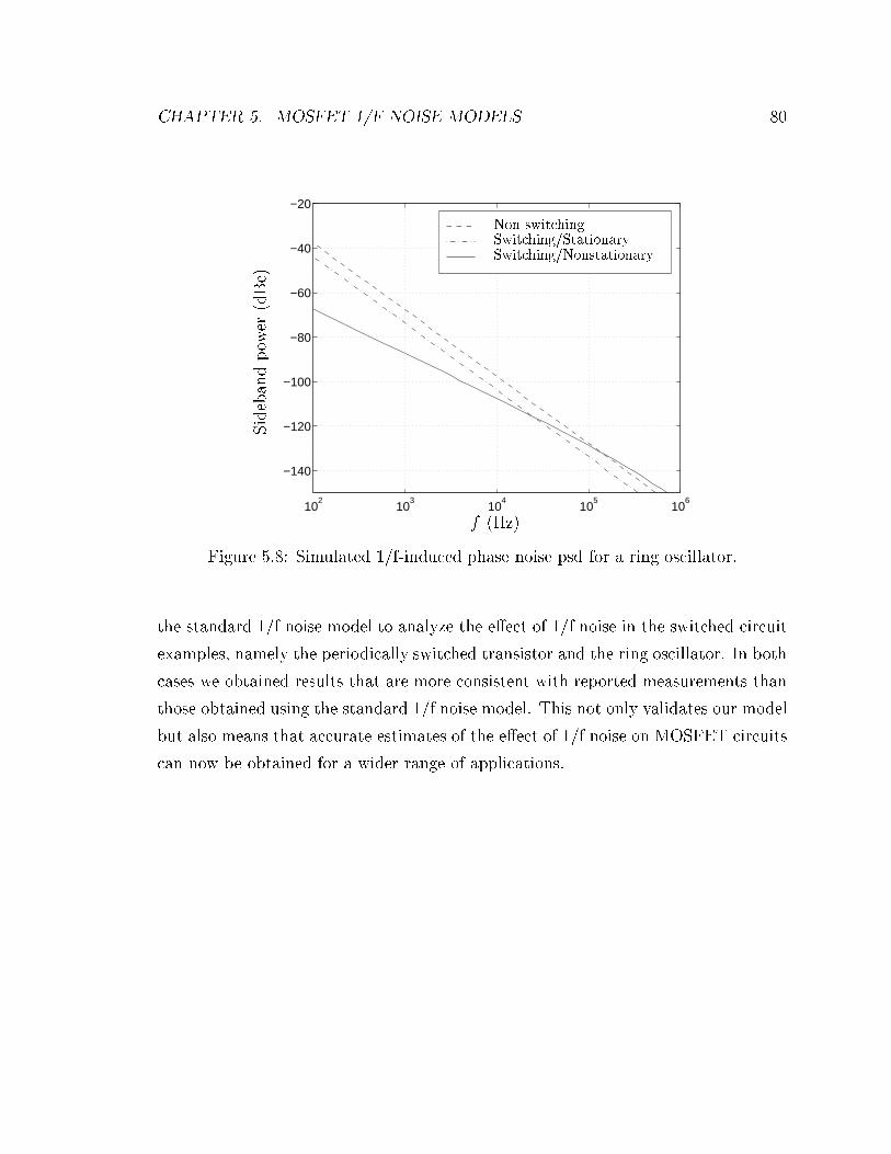
CHAPTER 5. MOSFET 1/F NOISE MODELS 80
102
103
104
105
106
−140
−120
−100
−80
−60
−40
−20
f (Hz)
Sidebandpower(dBc)
Switching/NonstationarySwitching/StationaryNon-switching
Figure 5.8: Simulated 1/f-induced phase noise psd for a ring oscillator.
the standard 1/f noise model to analyze the e�ect of 1/f noise in the switched circuit
examples, namely the periodically switched transistor and the ring oscillator. In both
cases we obtained results that are more consistent with reported measurements than
those obtained using the standard 1/f noise model. This not only validates our model
but also means that accurate estimates of the e�ect of 1/f noise on MOSFET circuits
can now be obtained for a wider range of applications.
Chapter 6
Analysis of 1/f Noise in CMOS
APS
6.1 Introduction
1/f noise in image sensors has been under study for many years [43, 26]. Because 1/f
noise is concentrated in low frequency range, human eye is particularly sensitive to
its e�ect. To estimate the noise power due to 1/f noise in a CMOS APS, frequency
domain analysis is typically performed using the standard 1/f noise model. A low
cuto� frequency fL that is inversely proportional to the circuit on-time is typically
used to get reasonable noise power estimates. The choice of this low cuto� frequency
is quite arbitrary, however, and can cause signi�cant inaccuracy in estimating noise
power. Moreover, during reset the circuit is not in steady state and thus frequency
domain analysis is inappropriate.
To more accurately estimate 1/f noise in CMOS APS, we use the time domain
analysis methods developed in chapter 3 and the nonstationary 1/f noise model de-
rived in chapter 5 to perform the noise analysis. We again use the photodiode APS
circuit as an example, which is shown in Figure 2.14. For simplicity, we will �rst
�nd the 1/f noise RMS value at node Bitline in volts. To compute this value, we
consider the 1/f noise generated during each step of the APS operation, i.e., during
reset, integration, and readout. Once the Bitline referred 1/f noise is determined, it
81
CHAPTER 6. ANALYSIS OF 1/F NOISE IN CMOS APS 82
is straightforward to get the input referred or output referred 1/f noise power using
the corresponding circuit transfer functions.
During reset, the 1/f noise is caused by the reset transistor. This transistor is
working most of the time in subthreshold and has time varying small signal circuit
model. During integration, the 1/f noise is primarily generated by the photodiode.
It is due to surface recombination of carriers, and the uctuation in bulk carrier
mobility [44]. For a reverse biased photodiode, the 1/f noise is not directly related to
the total current. Instead, it is a function of the dark current, and is typically much
smaller than the dark current shot noise, and can thus be ignored. During readout,
1/f noise is mainly due to the pixel level transistors, including follower transistor
and access transistor. Column and chip level transistors also cause 1/f noise, which
however can be easily reduced to negligible level by simply increasing the transistor
area.
The rest of the chapter is organized as follows. In section 6.2 we analyze the 1/f
noise due to the follower and the access transistors using time domain analysis and
our nonstationary 1/f noise model. We �nd that the results are approximately twice
as large as the results obtained using frequency domain analysis assuming normal
readout speed. In section 6.3 we analyze the 1/f noise due to the reset transistor.
Here we use the subthreshold time varying circuit model in addition to our nonsta-
tionary noise model. We �nd that the conventional frequency domain results are very
inconsistent and very inaccurate: over a factor of 11 lower than time domain analysis
in some cases. We isolate the e�ect of noise model and �nd that nonstationary noise
model produces results that are more consistent with experiments that the standard
model does.
6.2 1/f Noise Due to the Follower and Access Tran-
sistors
During readout, the 1/f noise is mainly due to the source follower transistor M2, and
the access transistor M3. Depicted in Figure 6.1 is the small signal model of the APS
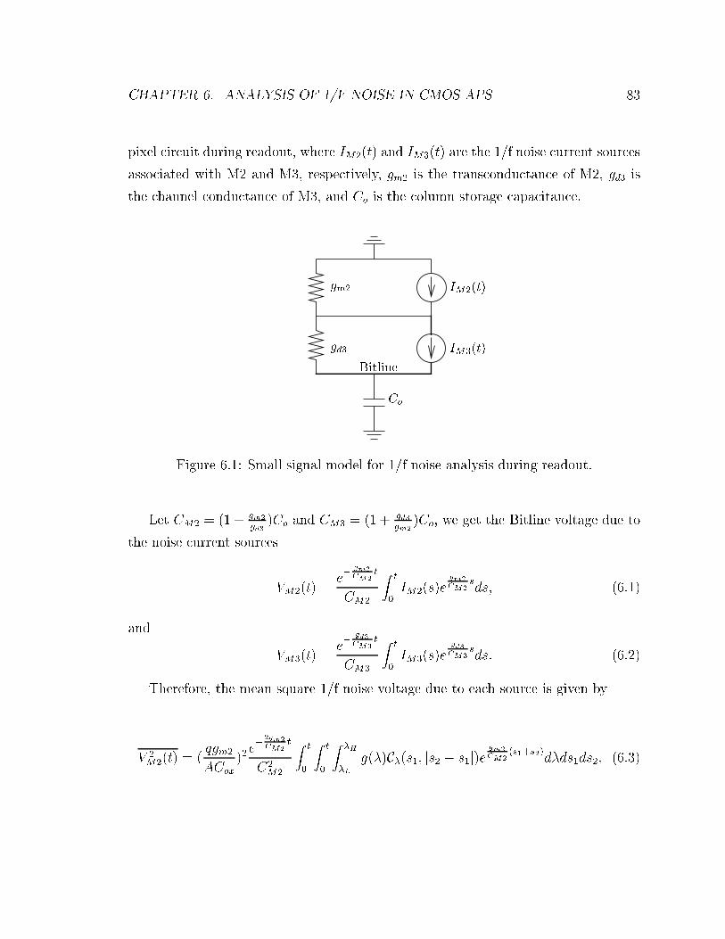
CHAPTER 6. ANALYSIS OF 1/F NOISE IN CMOS APS 83
pixel circuit during readout, where IM2(t) and IM3(t) are the 1/f noise current sources
associated with M2 and M3, respectively, gm2 is the transconductance of M2, gd3 is
the channel conductance of M3, and Co is the column storage capacitance.
IM2(t)
IM3(t)
Co
gm2
gd3
Bitline
Figure 6.1: Small signal model for 1/f noise analysis during readout.
Let CM2 = (1+ gm2
gd3)Co and CM3 = (1+ gd3
gm2)Co, we get the Bitline voltage due to
the noise current sources
VM2(t) =e�
gm2CM2
t
CM2
Zt
0IM2(s)e
gm2CM2
sds; (6.1)
and
VM3(t) =e�
gd3
CM3t
CM3
Zt
0IM3(s)e
gd3CM3
sds: (6.2)
Therefore, the mean square 1/f noise voltage due to each source is given by
V 2M2(t) = (
qgm2
ACox
)2e�
2gm2CM2
t
C2M2
Zt
0
Zt
0
Z�H
�L
g(�)C�(s1; js2 � s1j)egm2CM2
(s1+s2)d�ds1ds2; (6.3)
CHAPTER 6. ANALYSIS OF 1/F NOISE IN CMOS APS 84
and
V 2M3(t) = (
qgm3
ACox
)2e�
2gd3
CM3t
C2M3
Zt
0
Zt
0
Z�H
�L
g(�)C�(s1; js2 � s1j)egd3CM3
(s1+s2)d�ds1ds2: (6.4)
As a numerical example, we assume that the nMOS transistor mobility is � =
550cm2V�1s�1, the bias current is id = 1:8�A, the reverse bias voltage on the photo-
diode is vpd = 1:8V, and the threshold voltage is vth = 0:9V (with body e�ect). The
transconductance of M2 thus is
gm2 �
q2id�CoxW=L = 4:4� 10�5�1:
Since M3 is operating in the linear region and the voltage di�erence between its
drain and source is very small, we can write
gd3 � �CoxW=L(vG3 � vD3 � vth); (6.5)
where vG3 = 3:3V is the gate voltage of M3. Note that
vD3 = vpd �
s2id
�CoxW=L� vth:
Substituting into equation 6.5, we get that gd3 = 8:7 � 10�4�1. Consequently the
transconductance of M3
gm3 �id
vG3 � vS3 � vth= 1:1� 10�6�1:
Now we can numerically evaluate equations 6.3 and 6.4 to �nd the Bitline RMS
noise voltages due to M2 and M3, as functions of the pixel readout time tread. The
results are plotted in Figure 6.2 and Figure 6.3, together with the RMS 1/f noise
voltages calculated using the frequency domain method. Assuming the pixel readout
time of 1�s, the RMS 1/f noise voltage is about 63�V due to follower transistor, and
below 1�V due to access transistor. They are twice as large as the values obtained
using frequency domain method. The di�erence between the results computed using
CHAPTER 6. ANALYSIS OF 1/F NOISE IN CMOS APS 85
the nonstationary model and the stationary model, as expected, is decreasing as tread
gets larger. This is because the traps are approaching their steady states. Also
plotted in the �gure are the noise voltages due to thermal noise. Note that RMS
1/f noise voltage is higher than thermal noise voltage for the follower transistor, but
much lower than thermal noise voltage for the access transistor. The reason for this
di�erent behavior is that the follower transistor is working in saturation regime, while
the access transistor is working in linear regime. In saturation regime, both thermal
and 1/f noise is proportional to the transconductance. In linear regime, 1/f noise is
still proportional to the transconductance, while thermal noise is proportional to the
channel conductance, which can be much higher than the transconductance.
There is another importance fact that worth pointing out. It is well known that
by increasing the storage capacitance Co the output thermal noise power can be
e�ectively reduced, because the readout circuit bandwidth is reduced. Increasing Co
or reducing bandwidth, however, has no observable e�ects on the output 1/f noise
power. Since 1/f noise energy is concentrated in low frequency range, the reduction
of bandwidth cannot be used to e�ectively reduce 1/f noise power.
6.3 1/f Noise Due to the Reset Transistor
During reset, the 1/f noise is mainly due to the reset transistor. The source follower
reset circuit is not only used in the pixel circuit of a CMOS APS, it is also commonly
used in the output stage of a CCD image sensor. As depicted in Figure 6.4 during
reset, the gate of the transistor is set to a high voltage vreset for a short period of time
tr. To �nd the output noise power due to the transistor 1/f noise, frequency domain
analysis is typically performed using the standard 1/f noise model to get
V 2out(tr) = 2
Z1
1tr
SId(f)
g2m(tr) + 4�2f 2C2
df;
where gm is the transistor transconductance, and SId is the transistor drain current
1/f noise psd. The choice of 1tras a low cuto� frequency is quite arbitrary, however.
Moreover the circuit is not is steady state [51] and thus it is inappropriate to use
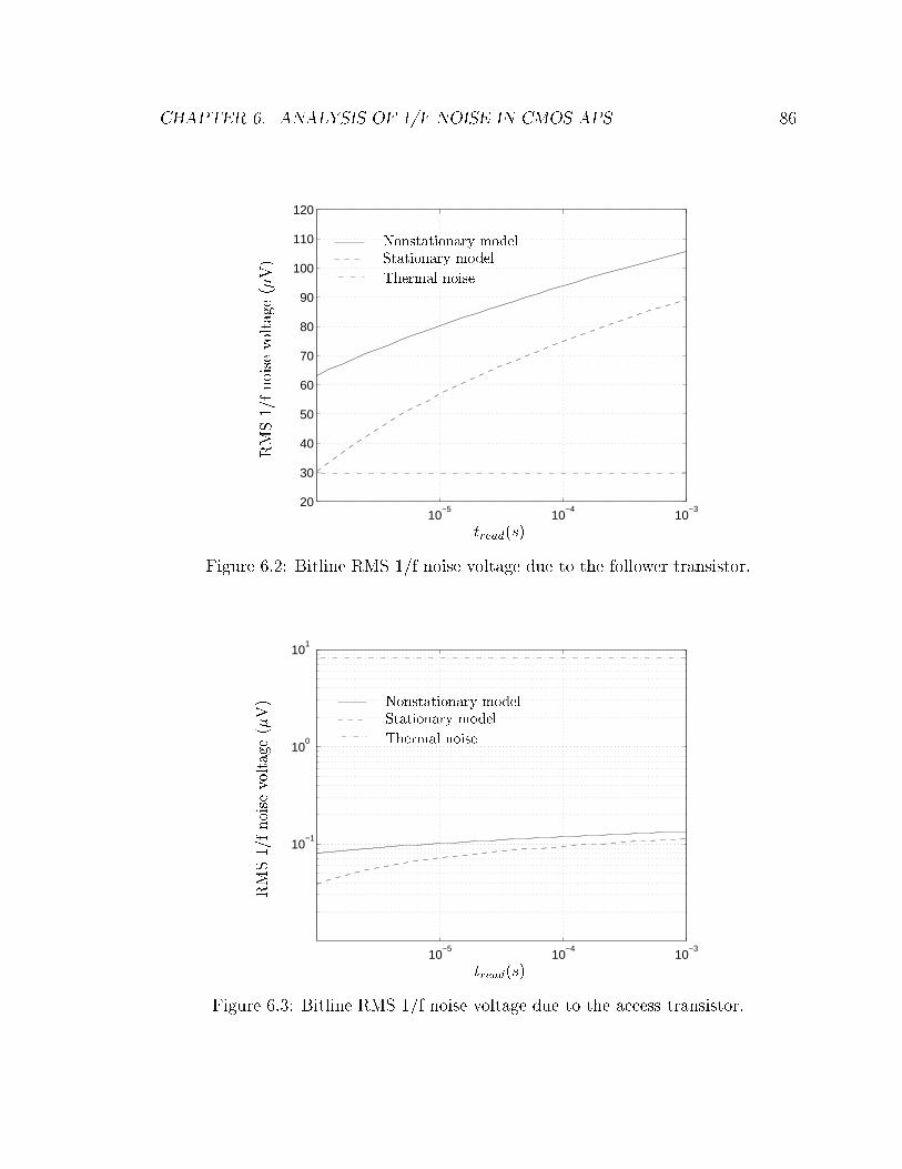
CHAPTER 6. ANALYSIS OF 1/F NOISE IN CMOS APS 86
10−5
10−4
10−3
20
30
40
50
60
70
80
90
100
110
120
tread(s)
RMS1/fnoisevoltage(�V)
Nonstationary modelStationary model
Thermal noise
Figure 6.2: Bitline RMS 1/f noise voltage due to the follower transistor.
10−5
10−4
10−3
10−1
100
101
tread(s)
RMS1/fnoisevoltage(�V) Nonstationary model
Stationary model
Thermal noise
Figure 6.3: Bitline RMS 1/f noise voltage due to the access transistor.
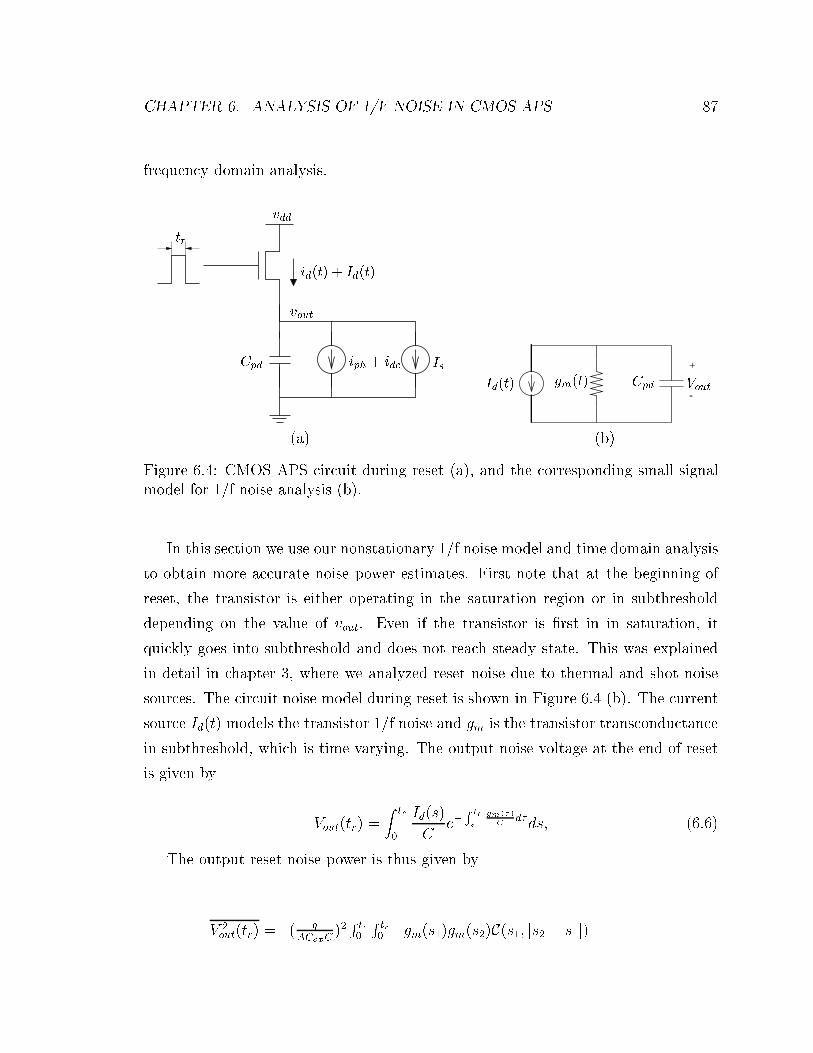
CHAPTER 6. ANALYSIS OF 1/F NOISE IN CMOS APS 87
frequency domain analysis.
tr
vdd
vout
Cpd
id(t) + Id(t)
iph + idc Is +
-Id(t) gm(t) Cpd Vout
(a) (b)
Figure 6.4: CMOS APS circuit during reset (a), and the corresponding small signal
model for 1/f noise analysis (b).
In this section we use our nonstationary 1/f noise model and time domain analysis
to obtain more accurate noise power estimates. First note that at the beginning of
reset, the transistor is either operating in the saturation region or in subthreshold
depending on the value of vout. Even if the transistor is �rst in in saturation, it
quickly goes into subthreshold and does not reach steady state. This was explained
in detail in chapter 3, where we analyzed reset noise due to thermal and shot noise
sources. The circuit noise model during reset is shown in Figure 6.4 (b). The current
source Id(t) models the transistor 1/f noise and gm is the transistor transconductance
in subthreshold, which is time varying. The output noise voltage at the end of reset
is given by
Vout(tr) =
Ztr
0
Id(s)
Ce�
Rtr
s
gm(�)C
d�ds; (6.6)
The output reset noise power is thus given by
V 2out(tr) = ( q
ACoxC)2Rtr
0
Rtr
0 gm(s1)gm(s2)C(s1; js2 � s1j)
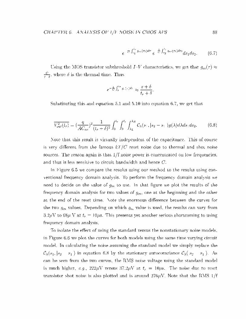
CHAPTER 6. ANALYSIS OF 1/F NOISE IN CMOS APS 88
e�
1C
Rtr
s1gm(�1)d�1
e�
1C
Rtr
s2gm(�2)d�2
ds1ds2: (6.7)
Using the MOS transistor subthreshold I{V characteristics, we get that gm(�) �
C
�+Æ, where Æ is the thermal time. Thus
e�
1C
Rtr
sgr(�)d� �
s+ Æ
tr + Æ:
Substituting this and equation 5.1 and 5.10 into equation 6.7, we get that
V 2out(tr) = (
q
ACox
)21
(tr + Æ)2
Ztr
0
Ztr
0
Z�H
�L
C�(s1; js2 � s1j)g(�)d�ds1ds2: (6.8)
Note that this result is virtually independent of the capacitance. This of course
is very di�erent from the famous kT=C reset noise due to thermal and shot noise
sources. The reason again is that 1/f noise power is concentrated on low frequencies,
and thus is less sensitive to circuit bandwidth and hence C.
In Figure 6.5 we compare the results using our method to the results using con-
ventional frequency domain analysis. To perform the frequency domain analysis we
need to decide on the value of gm to use. In that �gure we plot the results of the
frequency domain analysis for two values of gm, one at the beginning and the other
at the end of the reset time. Note the enormous di�erence between the curves for
the two gm values. Depending on which gm value is used, the results can vary from
3:2�V to 68� V at tr = 10�s. This presents yet another serious shortcoming to using
frequency domain analysis.
To isolate the e�ect of using the standard versus the nonstationary noise models,
in Figure 6.6 we plot the curves for both models using the same time varying circuit
model. In calculating the noise assuming the standard model we simply replace the
C�(s1; js2 � s1j) in equation 6.8 by the stationary autocovariance C�(js2 � s1j). As
can be seen from the two curves, the RMS noise voltage using the standard model
is much higher, e.g., 222�V versus 37:2�V at tr = 10�s. The noise due to reset
transistor shot noise is also plotted and is around 276�V. Note that the RMS 1/f
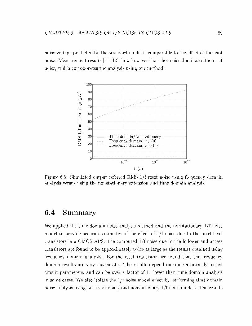
CHAPTER 6. ANALYSIS OF 1/F NOISE IN CMOS APS 89
noise voltage predicted by the standard model is comparable to the e�ect of the shot
noise. Measurement results [51, 42] show however that shot noise dominates the reset
noise, which corroborates the analysis using our method.
10−5
10−4
10−3
0
10
20
30
40
50
60
70
80
90
100
tr(s)
RMS1/fnoisevoltage(�V)
Time domain/NonstationaryFrequency domain, gm1(0)Frequency domain, gm1(tr)
Figure 6.5: Simulated output referred RMS 1/f reset noise using frequency domain
analysis versus using the nonstationary extension and time domain analysis.
6.4 Summary
We applied the time domain noise analysis method and the nonstationary 1/f noise
model to provide accurate estimates of the e�ect of 1/f noise due to the pixel level
transistors in a CMOS APS. The computed 1/f noise due to the follower and access
transistors are found to be approximately twice as large as the results obtained using
frequency domain analysis. For the reset transistor, we found that the frequency
domain results are very inaccurate. The results depend on some arbitrarily picked
circuit parameters, and can be over a factor of 11 lower than time domain analysis
in some cases. We also isolate the 1/f noise model e�ect by performing time domain
noise analysis using both stationary and nonstationary 1/f noise models. The results
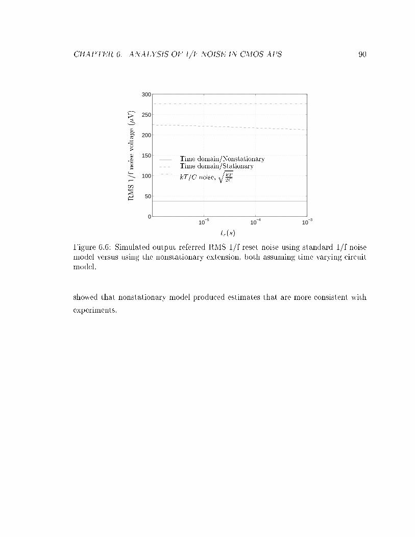
CHAPTER 6. ANALYSIS OF 1/F NOISE IN CMOS APS 90
10−5
10−4
10−3
0
50
100
150
200
250
300
tr(s)
RMS1/fnoisevoltage(�V)
Time domain/NonstationaryTime domain/Stationary
kT=C noise,
qkT
2C
Figure 6.6: Simulated output referred RMS 1/f reset noise using standard 1/f noise
model versus using the nonstationary extension, both assuming time varying circuit
model.
showed that nonstationary model produced estimates that are more consistent with
experiments.
Chapter 7
Conclusion
7.1 Summary
We have presented the �rst complete and rigorous analysis of temporal noise in CMOS
image sensors. It takes the time varying circuit models and nonstationary noise
sources into consideration.
Using time domain analysis, instead of the more traditional frequency domain
analysis method, we found that the reset noise power due to thermal noise is at most
half of its commonly quoted KTC value. This fundamental result was corroborat-
ed by several published experimental data including data collected in our lab. The
lower reset noise, however, comes at the expense of image lag. We found that alter-
native reset methods such as overdriving the reset transistor gate or using a pMOS
transistor can alleviate lag, but double the reset noise power. We proposed a new
reset method that alleviates lag without increasing reset noise. We analyzed noise
due to the photodetector shot noise taking nonlinearity into consideration and found
that nonlinearity improves SNR at high illumination. We also analyzed noise during
readout using both hand analysis and SPICE simulation.
We have developed methods for CMOS image sensors characterization. We char-
acterized the 64�64 CMOS APS test structure fabricated in a 0.35� standard digital
CMOS process. We found that the measured reset noise is indeed very close to the
half kT/C result derived in previous chapter. The measured SNR is also consistent
91
CHAPTER 7. CONCLUSION 92
with the calculated shot noise using our nonlinear model. We also demonstrated the
incomplete reset induced image lag.
We have proposed a nonstationary extension to the standard 1/f noise model. The
model is based on the fact that the active traps are mostly empty when the MOSFET
is o�. By modifying the RTS model for a single trap to re ect this fact, the noise
autocovariance function can be numerically evaluated. We used our nonstationary
extension of the standard 1/f noise model to analyze the e�ect of 1/f noise in the
switched circuit examples, namely the periodically switched transistor and the ring
oscillator. In both cases we obtained results that are more consistent with reported
measurements than those obtained using the standard 1/f noise model. This not only
validates our model but also means that accurate estimates of the e�ect of 1/f noise
on MOSFET circuits can now be obtained for a wider range of applications.
We have applied the time domain noise analysis method and the nonstationary
1/f noise model to provide accurate estimates of the e�ect of 1/f noise due to the pixel
level transistors in a CMOS APS. The computed 1/f noise due to the follower and
access transistors are found to be approximately twice as large as the results obtained
using frequency domain analysis. For the reset transistor, we found that the frequency
domain results are very inaccurate. The results depend on some arbitrarily picked
circuit parameters, and can be over a factor of 11 lower than time domain analysis
in some cases. We also isolate the 1/f noise model e�ect by performing time domain
noise analysis using both stationary and nonstationary 1/f noise models. The results
showed that nonstationary model can produce estimates that are more consistent
with experiments.
Since temporal noise sets the fundamental limit on image sensor performance, it
is very important to be able to accurately estimates the temporal noise power. We
believe that the thesis contributes to better understand the noise mechanism and
thus leads to further noise suppression. This serves the purpose of improving imaging
quality of CMOS image sensors, and making it a superior choice among imaging
devices.
CHAPTER 7. CONCLUSION 93
7.2 Future Work and Future Directions
In the thesis we analyzed the intrinsic noise, including thermal, shot, and 1/f noise.
Other noise sources are generally reducible through judicious design practice. As
more functions are integrated onto the same chip that holds the image sensor, it
is, however, harder to suppress the noise due to those other noise sources. One such
example is the noise coupled into the sensor array from the peripheral circuits through
the substrate. When control, memory, and image processing blocks are integrated
together with the image sensors which might have over a million pixels, the cross talk
between the sensor array and those other function blocks becomes very strong and
hard to track. As a result, it is very diÆcult to identify and suppress the substrate
noise. A practical model that can eÆciently calculate the substrate noise e�ect will
extend our knowledge of noise behavior in CMOS image sensors, and will greatly
bene�t the design of the next generation of highly integrated image sensor systems.
While pursuing higher level integration, further image quality improvement is
also indispensable for CMOS image sensors. It is crucial to extend the use of CMOS
image sensors into high end imaging applications. The thesis focuses on how noise
sets a fundamental limit on dynamic range and signal to noise ratio. It would be
useful to extend the work to also consider the relationship between noise and other
important image sensor parameters. For example, since each pixel has di�erent 1/f
noise characteristics, the 1/f noise may appear as di�erent DC o�sets among the
pixels. As these pixels are independent, the 1/f drift will be di�erent and the pattern
will change with time. This time varying \�xed" pattern noise can cause problem for
video application. Noise may also change the sensor color response. In a color �lter
array based CMOS image sensors, the di�erent noise added to di�erent pixels may
cause distorted color. Since human observer is more sensitive to the color distortion
than to the magnitude variation, it is important to fully understand the e�ect of
temporal noise on color image sensors.
To keep scaling the CMOS image sensors to even smaller pixel size and larger
format, without sacri�ce the image quality, the requirement of low noise operation
becomes more strict. Because the full well electron capacity and quantum eÆciency
CHAPTER 7. CONCLUSION 94
are generally reduced, the signal is becoming weaker, and thus it is desirable to
minimize the noise level. Noise on the other hand, cannot be reduced at will. It would
be interesting to �nd out if noise imposes limits on the sensor scaling. Similar question
can be asked for QE, full well electron capacity, and other parameters. Identifying
the limiting factor may help us to break the barrier of CMOS image sensor scaling.
Design for testing is another important �eld that needs improvement. The CMOS
image sensors is in general hard to test, because it involves optoelectronic response,
mixed signal operation, and has very limited area per pixel. Increased testability will
greatly improve the characterization accuracy, and thus help to identify the bottleneck
in sensor design. For example, the extra drain voltage line of the reset transistor has
been used to test the readout circuit response, which helped to better estimate the
sensor sense node capacitance, quantum eÆciency, noise, and many other parameters.
Improvements of testability, however, must be done without adversely a�ecting the
sensor performance.
The nonstationary 1/f noise model presented in the thesis has been used to analyze
switched circuits including CMOS image sensors. It would be interesting to apply
the model to analyze other circuits as well. The better understanding of 1/f noise
behavior may lead to some novel 1/f noise reduction scheme. The model itself can
also be improved, e.g., by re�ning the modeling of the trap states when the transistor
is switched from on to o�.
Finally, multiple sampling has been demonstrated to greatly improve image sen-
sor dynamic range by virtually increasing the well capacity. It is worth thinking if
multiple sampling can also be applied to eÆciently reduce noise oor, thus increas-
ing both dynamic range and sensitivity. One simple algorithm is to average all the
samples. By intelligently picking the sampling time one can expect to achieve higher
noise reduction.
Bibliography
[1] I. Bloom and Y. Nemirovsky. 1/f Noise Reduction of Metal-Oxide-Semiconductor
Transistors by Cycling From Inversion to Accumulation. Applied Physics Letters,
58(15):1664{1666, April 1991.
[2] T. Boutchacha, G. Ghibaudo, G. Guegan, and T. Skotnicki. Low Frequency
Noise Characterization of 0.18um Si CMOS Transistors. Microelectron. Reliab.,
37(10/11):1599{1602, 1997.
[3] P. Centen. CCD On-Chip Ampli�ers: Noise Performance versus MOS Transistor
Dimensions. IEEE Trans. Electron Devices, 38(5):1206{1216, May 1991.
[4] J. Chang, A. A. Abidi, and C. R. Viswanathan. Flicker Noise in CMOS Tran-
sistors from Subthreshold to Strong Inversion at Various Temperatures. IEEE
Trans. Electron Device, 41(11):1965{1971, November 1994.
[5] S. Decker, D. McGrath, K. Brehmer, and C. G. Sodini. A 256 � 256 CMOS
Imaging Array with Wide Dynamic Range Pixels and Column{Parallel Digital
Output. IEEE J. Solid-State Circuits, 33(12):2081{2091, 1998.
[6] B. Dierickx and E. Simoen. The Decrease of "Random Telegraph Signal" Noise
in Metal-Oxide-Semiconductor Field-E�ect Transistors When Cycled From In-
version to Accumulation. J. Applied Physics, 71(4):2028{2029, February 1992.
[7] A. El Gamal, B. Fowler, H. Min, and X. Liu. Modeling and Estimation of
FPN Components in CMOS Image Sensors. In Proc. SPIE, volume 3301, pages
168{177, San Jose, CA, Jan. 1998.
95
BIBLIOGRAPHY 96
[8] R. Forchheimer and A. Odmark. A Single Chip Linear Array Processor, in
Applications of digital image processing. SPIE, 1983.
[9] R. Forchheimer, P.Ingelhag, and C. Jansson. MAPP2200, a second generation
smart optical sensor. SPIE, 1992.
[10] E. R. Fossum. Active Pixel Sensors: are CCD's dinosaurs. In Proceedings of
SPIE, pages 2{14, San Jose, CA, February 1993.
[11] E. R. Fossum. CMOS Image Sensors: Electronic Camera On A Chip. In Proceed-
ings of International Electron Devices Meeting, pages 17{25, Washington, DC,
December 1995.
[12] B. Fowler, A. El Gamal, D. Yang, and H. Tian. A Method for Estimating
Quantum EÆciency for CMOS Image Sensors. In Proc. SPIE, volume 3301,
pages 178{185, San Jose, CA, Jan. 1998.
[13] B. Fowler, A. El Gamal, and D. X. D. Yang. \A CMOS Area Image Sensor
with Pixel-Level A/D Conversion". In ISSCC Digest of Technical Papers, San
Fransico, CA, February 1994.
[14] B. Fowler, D. Yang, H. Min, and A. El Gamal. Single Pixel Test Structures for
Comparative Analysis of CMOS Image Sensors. In 1997 IEEE Work Shop on
CCDs and AIS, Brugge, Belgium, June 1997.
[15] S. L. J. Gierkink, E. A. M. Klumperink, A. P. van der Wel, G. Hoogzaad, E. van
Tuijl, and B. Nauta. Intrinsic 1/f Device Noise Reduction and Its E�ect on Phase
Noise in CMOS Ring Oscillators. IEEE J. Solid-State Circuits, 34(7):1022{1025,
July 1999.
[16] P.R. Gray and R.G. Meyer. Analysis and Design of Analog Integrated Circuits.
John Wiley & Sons, Inc., New York, 1993.
[17] A. Hajimiri and T. H. Lee. A General Theory of Phase Noise in Electrical
Oscillators. IEEE J. Solid-State Circuits, 33(2):179{194, February 1998.
BIBLIOGRAPHY 97
[18] A. Hajimiri, S. Limotyrakis, and T. H. Lee. Jitter and Phase Noise in Ring
Oscillators. IEEE J. Solid-State Circuits, 34(6):790{804, June 1999.
[19] G. C. Holst. CCD Arrays Cameras and Displays: second edition. JCD Publish-
ing, 1998.
[20] C. Hu, G. P. Li, E. Worley, and J. White. Consideration of Low-Frequency
Noise in MOSFET's for Analog Performance. IEEE Electron Device Letters,
17(12):552{554, December 1996.
[21] C. D. Hull and R. G. Meyer. A Systematic Approach to the Analysis of Noise
in Mixers. IEEE Trans. Circuits Syst., 40(12):909{919, December 1993.
[22] K. K. Hung, P. K. Ko, C. Hu, and Y. C. Cheng. A Uni�ed Model for the Flick-
er Noise in Metal-Oxide-Semiconductor Field-E�ect Transistors. IEEE Trans.
Electron Device, 37(3):654{665, March 1990.
[23] J. Hynecek. Spectral Analysis of Reset Noise Observed in CCD Charge-Detection
Circuits. IEEE Trans. Electron Devices, 37(3):640{647, Mar. 1990.
[24] C. Jakobson, I. Bloom, and Y. Nemirovsky. 1/f Noise in CMOS Transistors for
Analog Applications From Subthreshod to Saturation. Solid-State Electronics,
42(10):1807{1817, 1998.
[25] J. Janesick et al. Charge-coupled-device response to electron beam energies of
less than 1 keV up to 20 keV. Optical Engineering, 26(8):686{91, August 1987.
[26] J. F. Johnson. Methodology for Simulating 1/f Noise Characteristics in the Time
Domain for Infrared Focal Plane Applications. In Proc. the SPIE, pages 31{37,
Orlando, Florida, April 1997.
[27] J. S. Kim, C. H. Park, and H. S. Min adn Y. J. Park. Theory of 1/f Noise
Current in n+p Diodes, n+p Photodiodes, and Schottky Diodes. In Quantum
1/f Noise and Other Low Frequency Fluctuations in Electronic Devices: Seventh
Symposium, pages 123{128, 1999.
BIBLIOGRAPHY 98
[28] M. J. Kirton and M. J. Uren. Noise in Solid-State Microstructures: A New Per-
spective on Individual Defects, Interface States and Low-frequency (1/f) Noise.
Advances in Physics, 38(4):367{468, 1989.
[29] D. G. Lampard. Generalization of the Wiener-Khintchine Theorem to Nonsta-
tionary Processes. J. Applied Physics, 25(6):802{803, June 1954.
[30] M. Loinaz, K. Singh, A. Blanksby, D. Inglis, K. Azadet, and B. Ackland.
A 200mW 3.3V CMOS color camera IC producing 352x288 24b Video at
30frames/s. In ISSCC Digest of Technical Papers, pages 168{169, San Fran-
sisco, CA, February 1998.
[31] C. Mead. Analog VLSI and Neural Systems. Addison Wesley, 1989.
[32] S. Mendis et al. Progress in CMOS Active Pixel Image Sensors. In Proceedings
of SPIE, pages 19{29, San Jose, CA, February 1994.
[33] S. Mendis, E. R. Fossum, et al. A 128�128 CMOS Active Pixel for Highly
Integrated Imaging Systems. In IEEE IEDM Technical Digest, San Jose, CA,
December 1993.
[34] S. K. Mendis, S. E. Kemeny, R. C. Gee, B. Pain, C. O. Staller, Q. Kim, and
E. R. Fossum. CMOS Active Pixel Image Sensors for Highly Integrated Imaging
Systems. IEEE J. Solid-State Circuits, 32(2):187{197, 1997.
[35] R.S. Muller and T.I. Kamins. DEVICE ELECTRONICS FOR INTEGRATED
CIRCUITS. Wiley, 1986.
[36] R. Panicacci et al. 128 Mb/s Multiport CMOS Binary Active-Pixel Image Sensor.
In ISSCC96 Techincal Digest, February 1996.
[37] P.Denyer, D. Renshaw, G. Wang, and M. Lu. A Single-Chip Video Camera with
On-Chip Automatic Exposure Control. In ISIC-91, 1991.
[38] P.Denyer, D Renshaw, G. Wang, and M. Lu. CMOS Image Sensors For Multi-
media Applications. In CICC93, 1993.
BIBLIOGRAPHY 99
[39] P.Denyer, D. Renshaw, G. Wang, M. Lu, and S.Anderson. On-Chip CMOS
Sensors for VLSI Imaging Systems. In VLSI-91, 1991.
[40] B. Razavi. A Study of Phase Noise in CMOS Oscillators. IEEE J. Solid-State
Circuits, 31(3):331{343, March 1996.
[41] J. Roychowdhury, D. Long, and P. Feldmann. Cyclostationary Noise Analysis
of Large RF Circuits with Multitone Excitations. IEEE J. Solid-State Circuits,
33(3):324{336, March 1998.
[42] R. Sarpeshkar, T. Delbruck, and C.A. Mead. White Noise in MOS Transistors
and Resistors. IEEE Circuits and Devices Magazine, 9(6):23{29, November 1993.
[43] D. A. Scribner, M. R. Kruer, J. C. Gridley, and K. Sarkady. Physical Limitations
to Nonuniformity Correction in IR Focal Plane Arrays. In Proc. the SPIE, pages
185{202, 1988.
[44] E. Simoen and C. L. Claeys. On the Geometry Dependence of the 1/f Noise in
CMOS Compatible Junction Diodes. IEEE Trans. Electron Device, 46(8):1725{
1732, August 1999.
[45] K. Singh. Noise Analysis of a Fully Integrated CMOS Image Sensor. In Proc.
SPIE, volume 3650, pages 44{51, San Jose, CA, Jan. 1999.
[46] S. Smith, J. Hurwitz, M. Torrie, D. Baxter, A. Holmes, M. Panaghiston, R. Hen-
derson, A. Murray, S. Anderson, and P. Denyer. A single-chip 306x244-pixel
CMOS NTSC video camera. In ISSCC Digest of Technical Papers, pages 170{
171, San Fransisco, CA, February 1998.
[47] T. Strom and S. Signell. Analysis of Periodically Switched Linear Circuits. IEEE
Trans. Circuits Syst., 24(10):531{541, October 1977.
[48] N. Teranishi, A. Kohono, Y. Ishihara, E. Oda, and K. Arai. No Image Lag
Photodiode Structure in the Interline CCD Image Sensor. IEDM Tech. Dig.,
pages 324{327, 1982.
BIBLIOGRAPHY 100
[49] A. J. P. Theuwissen. Solid-State Imaging with Charge-Coupled Devices. Kluwer
Academic Publishers, 1995.
[50] K. K. Thornber. Theory of Noise in Charge-Transfer Devices. Bell Sys. Tech.
J., 53(7):1211{1262, Sep. 1974.
[51] H. Tian, B. Fowler, and A. El Gamal. Analysis of Temporal Noise in CMOS
APS. In Proc. SPIE, volume 3649, pages 177{185, San Jose, CA, Jan. 1999.
[52] S. P. Tobin, S. Iwasa, and T. J. Tredwell. 1/f Noise in (Hg, Cd)Te Photodiodes.
IEEE Trans. Electron Device, 27(1):43{48, January 1980.
[53] A. van der Ziel. Noise in Solid State Devices and Circuits. Wiley, 1986.
[54] L. K. J. Vandamme, X. Li, and D. Rigaud. 1/f Noise in MOS Devices, Mobil-
ity or Number Fluctuations? IEEE Trans. Electron Device, 41(11):1936{1944,
November 1994.
[55] G.Weckler. Operation of p-n junction photodetectors in a photon ux integration
mode. IEEE Journal of Solid State Circuits, SC-2(3):65{73, 1967.
[56] O. Yadid-Pecht, B. Mansoorian, E. R. Fossum, and B. Pain. Optimization of
Noise and Responsivity in CMOS Active Pixel Sensors for Detection of Ultra
Low Light Levels. In Proc. SPIE, volume 3019, pages 125{136, San Jose, CA,
Feb. 1997.
[57] O. Yadid-Pecht, B. Pain, C. Staller, C. Clark, and E. R. Fossum. CMOS Active
Pixel Sensor Star Tracker with Regional Electronic Shutter. IEEE J. Solid-State
Circuits, 32(2):285{288, Feb. 1997.
[58] D. Yang, B. Fowler, and A. El Gamal. A 128�128 CMOS Image Sensor with
Multiplexed Pixel Level A/D Conversion. In CICC96, 1996.
[59] D. Yang, B. Fowler, A. El Gamal, H. Min, M. Beiley, and K. Cham. Test Struc-
tures for Characterization and Comparative Analysis of CMOS Image Sensors.
In Proc. SPIE, volume 2950, pages 8{17, Berlin, FRG, Oct. 1996.
BIBLIOGRAPHY 101
[60] D.X.D. Yang, A. El Gamal, B. Fowler, and H. Tian. A 640�512 CMOS Image
Sensor with Ultra Wide Dynamic Range Floating Point Pixel Level ADC. In
ISSCC Digest of Technical Papers, San Fransisco, CA, February 1999.


![Quantitative Study of High Dynamic Range Image Sensor ...abbas/group/papers_and_pub/ElecImaging04... · [Yang ‘99, Kleinfelder ‘01, Bidermann ‘03] Pixel 8Pixel-level ADC resolution](https://img.pdfslide.net/doc/110x75/5fb1647d2cfbc945de451f72/quantitative-study-of-high-dynamic-range-image-sensor-abbasgrouppapersandpubelecimaging04.jpg)