Embed Size (px)
Citation preview
16150 | Phys. Chem. Chem. Phys., 2014, 16, 16150--16157 This journal is© the Owner Societies 2014
Cite this:Phys.Chem.Chem.Phys.,
2014, 16, 16150
Non-conformal decoration of semiconductornanowire surfaces with boron nitride (BN)molecules for stability enhancement: degradation-resistant Zn3P2, ZnO and Mg2Si nanowires†
Venkata Vasiraju,a Yongmin Kanga and Sreeram Vaddiraju*ab
A simple and reliable strategy for stabilizing the surfaces of compound semiconductors was presented.
The strategy involved decorating the surfaces of compound semiconductor nanowires non-conformally
with small molecules of boron nitride (BN). More specifically, Zn3P2, ZnO and Mg2Si nanowires, highly
useful in energy conversion device fabrication (e.g., photovoltaics and thermoelectrics), have been
stabilized against air- and acid-assisted degradation by decorating their surfaces with small molecules of
BN. It is believed that the decoration of the nanowire surfaces with BN molecules made the nanowire
surfaces non-wettable to water and aqueous acid solutions, and thereby imparted them enhanced
resistance against water- and acid-assisted degradation. This procedure did not alter the bandgap of the
nanowires. Moreover, this procedure aided in retaining the electrical conduction between the nanowire
interfaces when the nanowires are assembled into mats or pellets. This strategy solves one of the
primary bottlenecks in the widespread use of nanowires in energy conversion device fabrication, namely
their stability. It is believed that this strategy is applicable for stabilizing other compound semiconductor
nanowires, including nitrides, sulfides, silicides and antimonides.
Introduction
Instability of inorganic compound semiconductors, especiallynanomaterials, is a subject that has received very little atten-tion, especially when compared to the volume of research thathas been/is being performed on nanomaterial synthesis, nano-material characterization and energy conversion device fabrica-tion from these materials.1–8 The need for addressing instabilityof compound semiconductor nanomaterials and devising stra-tegies for overcoming such instability is illustrated below usingthree material systems as examples, zinc phosphide (Zn3P2), zincoxide (ZnO) and magnesium silicide (Mg2Si) nanowires.
Zn3P2, an inorganic compound semiconductor, is predictedto be highly useful as a photoactive layer in the fabrication ofphotovoltaics (PVs).9,10 It is not only composed of earth abun-dant elements, Zn and P,11 but also has an ideal bandgap (Eg) of1.5 eV12 useful for obtaining the highest possible efficiencies insingle-junction PVs. It also has other characteristics ideal for
the fabrication of PVs, including high electron diffusionlengths of B10 mm reported in p-type Zn3P2 and a highabsorption coefficient 4104 cm�1.13–15 However, the instabilityof Zn3P2 prevents its widespread use in PV fabrication.16 It isunstable not only in ambient air at room temperature, but alsoin vacuum at slightly elevated temperatures of 150–200 1C.When exposed to air, Zn3P2 reacts with both oxygen andmoisture to form Zn(OH)2 or Zn3(PO4)2.17 Processing Zn3P2
under vacuum for the fabrication of PVs (e.g., metal cathodedeposition) also renders it unstable. It leads to loss of phos-phorus from the Zn3P2 surfaces.18 This inevitably leads to theformation of Zn–Zn3P2 interfaces dominating the electricalproperties of the interfaces, irrespective of the type of metaldeposited on their surfaces.19 The loss of phosphorus is believedto occur due to the rearrangement of the surfaces, followed bythe subsequent formation and sublimation of phosphorus in theform of P4 molecules. In addition to oxygen and moisture fromair, Zn3P2 also reacts with mild aqueous acid solutions. It reactswith mild HCl solution and forms ZnCl2, along with the evolu-tion of PH3 gas. As rainwater is acidic in nature (pH of rainwateris typically in the 5.5–6 range), this corrosion of Zn3P2 rendersany photovoltaic modules fabricated from it unsuitable forrooftop installation and long-term use. Similar instabilities arealso observed and reported in other compound semiconductors,including metal arsenides,20 antimonides21 and oxides.22
a Department of Materials Science and Engineering, Texas A&M University,
College Station, TX 77843, USA. E-mail: [email protected];
Fax: +1-979-845-6446; Tel: +1-979-862-1615b Artie McFerrin Department of Chemical Engineering, 3122 TAMU,
Texas A&M University, College Station, TX 77843, USA
† Electronic supplementary information (ESI) available. See DOI: 10.1039/c4cp01988a
Received 8th May 2014,Accepted 17th June 2014
DOI: 10.1039/c4cp01988a
www.rsc.org/pccp
PCCP
PAPER
Publ
ishe
d on
17
June
201
4. D
ownl
oade
d by
UN
IVE
RSI
TY
OF
AL
AB
AM
A A
T B
IRM
ING
HA
M o
n 26
/10/
2014
20:
27:4
7.
View Article OnlineView Journal | View Issue
This journal is© the Owner Societies 2014 Phys. Chem. Chem. Phys., 2014, 16, 16150--16157 | 16151
ZnO, similar to Zn3P2, is also a well-known semiconductorwith an Eg of 3.4 eV.23 It has been reported that ZnO nanowiresare useful in the fabrication of light emitting diodes (LEDs),24
waveguides25 and lasers,26 dye-sensitized solar cells (DSSCs)27
and biosensors.28 Similar to Zn3P2, the ZnO nanomaterial degrades(dissolves) in both acidic solutions of pH in the 4.5–5.0 range andbasic solutions of ammonia and NaOH, and even in horse bloodserum,29 rendering it unsuitable for the fabrication of stable energyconversion devices.
Finally, Mg2Si is a compound semiconductor highly useful inthe fabrication of thermoelectric modules.30–33 Similar to Zn3P2
and ZnO, Mg2Si reacts with both water and mild acid solutionsrendering it unsuitable for use in terrestrial thermoelectric devicefabrication. To illustrate the instability of Mg2Si, its reaction withwater and aqueous HCl solution is presented below:34,35
Mg2Si + 4H2O - 2Mg(OH)2 + SiH4
Mg2Si + 4HCl - 2MgCl2 + SiH4
In the past, passivation of surfaces with organic moleculeshas been pioneered to enhance the stability of inorganic semi-conductor surfaces.36,37 Both straight chain and conjugatedmolecules with various head groups have been employed forpassivating semiconductor surfaces as reported in the litera-ture.38 These molecules act as barriers and prevent the diffusionof either oxygen or moisture to the semiconductor surfaces,thereby imparting them enhanced resistance against air- andmoisture-assisted degradation.1,39 Although this strategy offersstability to semiconductors at low temperatures, it does not doso at high temperatures.40 In addition, these organic moleculesalter the interfacial properties of nanomaterials, especially whena multitude of these nanomaterials are assembled into devices.It is worthwhile to mention here that the presence of moleculesat the interfaces between assembled nanomaterials is not alwaysa handicap. In fact, the presence of molecules has been employedto tune thermal and electrical transport through materials. Never-theless the low stability of these organic molecules at hightemperatures necessitates the development of an alternate strat-egy for imparting stability to nanomaterials.
Therefore, the primary question that needs to be answered iswhether a strategy could be developed to enhance the stabilityof compound semiconductors at both room temperature andmoderately elevated temperatures. Of particular importancein the development of such strategies is ensuring that thestabilization process does not degrade/majorly alter either theirelectrical or their electronic properties. The aim of this paper isto accomplish the same, namely the development of a strategyfor making compound semiconductor nanowires stable both atroom temperature and at moderately high temperatures. Morespecifically, surface decoration of Zn3P2, ZnO and Mg2Si nano-wires with small and highly stable inorganic boron nitride (BN)molecules is presented as a strategy for imparting them stabi-lity against water- and acid-assisted degradation. In the end,it will be demonstrated that BN molecule decoration of nano-wire surfaces imparts them enhanced stability not only against
moisture-assisted degradation, but also to acid-assisted degrada-tion. It will also be demonstrated that such surface decorationdoes not adversely impact their electrical and electronic proper-ties (e.g., the electrical conductivities and the Eg of nanowires).Such inorganic molecule decoration of semiconductor nanowiresurfaces for making them corrosion resistant has never beenreported in the literature. Only a single report in the literaturediscussed the doping of semiconductors with salt molecules forenhancing their electrical conductivity.41 That report did notmention whether salt doping of semiconductors made themresistant to degradation.
Experimental methods
Zn3P2 and ZnO nanowires necessary for this study have beensynthesized using direct reaction schemes. This procedure hasbeen described in detail previously.17 Direct reaction of zinc foilwith either phosphorus or oxygen, respectively, was employedfor the synthesis of Zn3P2 and ZnO nanowires. These nanowiresynthesis experiments were performed in a hot-walled chemicalvapor deposition (HWCVD) chamber and in the presence ofhydrogen. The zinc foil served as both the source of zinc andthe substrate in these experiments. Following the synthesis,nanowires were brushed off the foil and collected as powders.The same HWCVD setup was slightly modified for obtaining BNmolecule decorated Zn3P2 and ZnO nanowire powders. Thismodified HWCVD setup is pictorially represented in Fig. S1 of theESI.† Experiments for obtaining BN molecule decorated nano-wires involved an additional step of exposing the nanowires to avapor of pre-decomposed B-tribromoborazine molecules immedi-ately after the formation of nanowires and before their removalfrom the vacuum chamber.17 The supply of B-tribromoborazinemolecules into the CVD chamber was accomplished by heatinga stainless-steel bubbler containing the source powder to atemperature of 300 1C. The B-tribromoborazine vapor was thenpassed through a decomposition zone maintained at a tem-perature of 600 1C,42 before it reacted with the nanowires. Inorder to prevent the complete conformal coating of the nano-wires with either a monolayer or multilayers of BN, only minuteamounts of B-tribromoborazine, B30–40 mg, were employedper experimental run. The amount of B-tribromoborazineemployed in each experimental run was always lower than thattheoretically required to form one monolayer of BN conformalcoating on top of all the nanowires synthesized in that run. Thenanowires obtained were characterized for morphology, phase,crystal structure and chemical composition using scanningelectron microscopy (SEM), X-ray diffraction (XRD), transmis-sion electron microscopy (TEM), and Fourier transform infra-red spectroscopy (FTIR). To understand the stability of BNmolecule decorated nanowires, they were dropped into eitherdeionized (DI) water or concentrated HCl solution (pH = 3) foran hour, followed by decanting the mixtures to collect the nano-wires and analyzing the so-obtained nanowires using electronmicroscopy and diffractometry. For comparison, as-obtained(or pristine) nanowires were also dropped into DI water and
Paper PCCP
Publ
ishe
d on
17
June
201
4. D
ownl
oade
d by
UN
IVE
RSI
TY
OF
AL
AB
AM
A A
T B
IRM
ING
HA
M o
n 26
/10/
2014
20:
27:4
7.
View Article Online
16152 | Phys. Chem. Chem. Phys., 2014, 16, 16150--16157 This journal is© the Owner Societies 2014
concentrated HCl solution, and the resulting residues were studiedusing microscopy and diffractometry. 4-Point probe measure-ments of nanowires cast into thin mats by drop casting nanowiredispersions were employed for the measurement of their electricalconductivities. UV-Vis spectroscopy was employed to determinethe Eg of both the BN decorated and as-obtained nanowires.23,43,44
While the characterization of Mg2Si nanowires was also per-formed using the methods mentioned above, their synthesis wasperformed using an alternate procedure. Mg2Si nanowires bothpristine and BN decorated were obtained by solid-state phasetransformation of pre-synthesized silicon nanowires produced byelectroless etching. The experimental procedure employed forobtaining Mg2Si nanowires has been described in detail pre-viously.45,46 For obtaining pristine Mg2Si nanowires, phase trans-formation of as-obtained silicon nanowires was performed. BNdecorated silicon nanowires (obtained by exposing silicon nano-wires to a vapor of decomposed B-tribromoborazine) were employedfor obtaining BN decorated Mg2Si nanowires.
Results and discussion
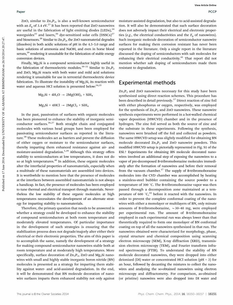
Scanning electron micrographs of pristine and BN moleculesurface decorated Zn3P2 nanowires are presented in Fig. 1a andb, respectively. As observed in the micrographs, the surfacedecoration of the nanowires, by itself, did not majorly altereither their morphologies or their dimensions. The diametersof both the pristine and BN decorated nanowires were observedto be approximately the same, in the range of 40–60 nm.A comparison of the XRD patterns of pristine and BN decoratednanowires (Fig. 1c) indicated that they are both composed ofonly a-Zn3P2 phase. No traces of any crystalline BN phase wasobserved in the BN molecule decorated Zn3P2 nanowires. Fromthe microscopy and diffractometry analyses, it can be con-cluded that the BN decoration process did not result in theformation of thick, conformal BN coatings on top of thenanowires, as such thick BN coating of the nanowires wouldhave significantly increased the diameter of the nanowires andindicated its presence in the XRD pattern. High-resolution TEM(HRTEM) and selected area electron diffraction (SAED) analysisof the pristine (Fig. 1d) and BN decorated nanowires (Fig. 1e)confirmed the conclusions drawn from the SEM and XRDanalyses and indicated that they are primarily composed ofa-Zn3P2 phase (Fig. 1d and e), and that exposure of thenanowires to decomposed B-tribromoborazine did not lead totheir conformal coating with BN (Fig. 1e). Furthermore, noformation of any nanoscale BN domains (or crystals) on top ofthe Zn3P2 nanowire surfaces was observed in the HRTEManalysis of BN decorated nanowires. Comparison of theHRTEM images of pristine and BN decorated nanowires(Fig. 1d and e, respectively) clearly indicated that their surfacesare different. Formation of amorphous Zn3(PO4)2 sheaths,expected on top of pristine Zn3P2 nanowires and observed ina previous study by our group, was clearly reiterated in Fig. 1d.In sharp contrast, the surfaces of BN decorated Zn3P2 nanowiresdid not indicate the presence of any Zn3(PO4)2 sheaths (Fig. 1e).
This result gave a preliminary indication that BN decoration ofZn3P2 nanowires prevented the reaction of their surfaces with airand the formation of amorphous Zn3(PO4)2 sheaths. Energydispersive spectroscopy (EDS) of the samples was also performedto detect the presence of BN on top of the nanowires (see Fig. S2of the ESI†). The analysis indicated the presence of no BN, clearlydemonstrating that the conformal coating of the nanowires withthick layers of either amorphous or crystalline BN did not occur.
To further probe the effect of BN surface decoration on thestability of Zn3P2 nanowires they were exposed to water andconcentrated HCl solution. Scanning electron micrographs ofBN molecule decorated Zn3P2 nanowires after they were treated
Fig. 1 Scanning electron micrographs of (a) pristine Zn3P2 nanowires and(b) BN decorated Zn3P2 nanowires. No changes in the morphologies or thedimensions of the nanowires were observed after they were decoratedwith BN. (c) XRD spectra of both pristine and BN decorated Zn3P2
nanowires. In both the cases, the nanowires exhibited the a-Zn3P2 phase.Peaks corresponding to zinc foil substrate employed for the synthesis ofnanowires are indicated with an * in the figure. Transmission electronmicrographs and the corresponding SAED patterns of (d) a pristine and (e)a BN decorated Zn3P2 nanowire. The analysis confirmed that the decora-tion process did not alter the phase of the nanowires, and indicated thatthe nanowires are not conformally coated with BN layers. TEM analysisalso indicated that the nanowires exhibited the [101] growth direction.
PCCP Paper
Publ
ishe
d on
17
June
201
4. D
ownl
oade
d by
UN
IVE
RSI
TY
OF
AL
AB
AM
A A
T B
IRM
ING
HA
M o
n 26
/10/
2014
20:
27:4
7.
View Article Online
This journal is© the Owner Societies 2014 Phys. Chem. Chem. Phys., 2014, 16, 16150--16157 | 16153
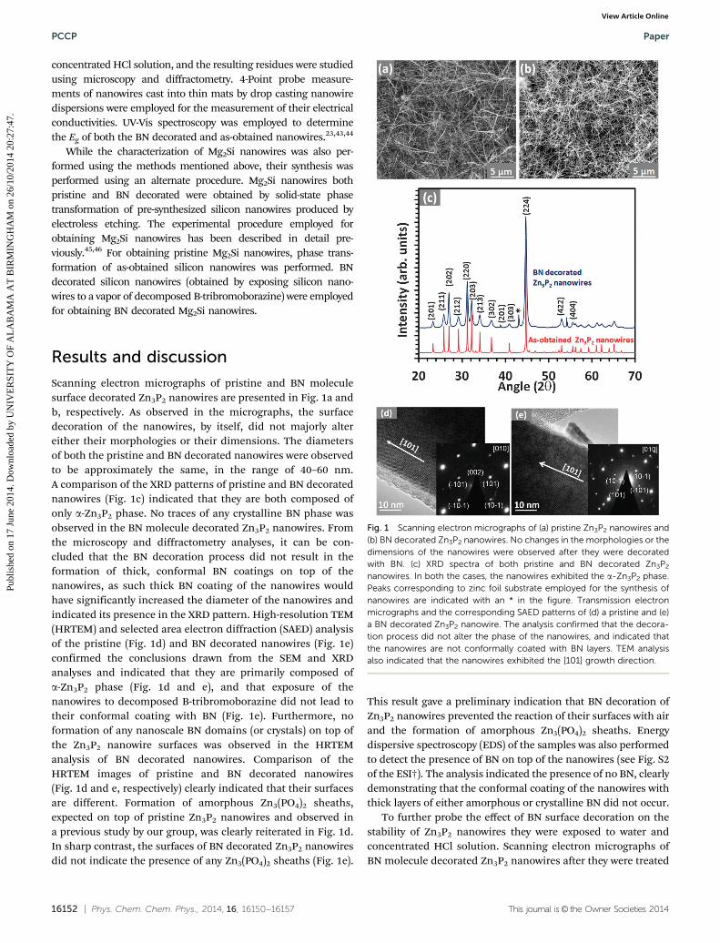
with deionized (DI) water and concentrated HCl solution ofpH 3 for one hour are respectively presented in Fig. 2a and b. Insharp contrast, pristine Zn3P2 nanowires indicated a completedegradation of the nanowire morphology after treatment witheither DI water or HCl solution of pH 3 for an hour (Fig. 2c and d,respectively).17 The XRD spectra of the nanowires after DI water
and acid treatments are presented in Fig. 2e. These analyses clearlyindicated that the morphology and the phase of the BN decoratedZn3P2 nanowires remained unaltered after either DI water or acidsolution treatment. HRTEM analysis of a BN decorated nanowireafter it is treated with HCl solution of pH 3 for one hour is depictedin Fig. 2f. The analysis indicated that the nanowire remainedsingle-crystalline and retained its a-Zn3P2 phase.
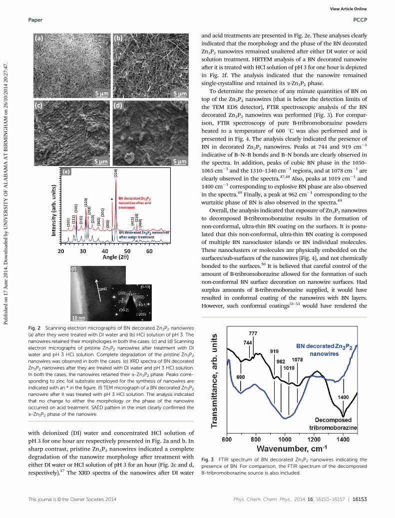
To determine the presence of any minute quantities of BN ontop of the Zn3P2 nanowires (that is below the detection limits ofthe TEM EDS detector), FTIR spectroscopic analysis of the BNdecorated Zn3P2 nanowires was performed (Fig. 3). For compar-ison, FTIR spectroscopy of pure B-tribromoborazine powdersheated to a temperature of 600 1C was also performed and ispresented in Fig. 4. The analysis clearly indicated the presence ofBN in decorated Zn3P2 nanowires. Peaks at 744 and 919 cm�1
indicative of B–N–B bonds and B–N bonds are clearly observed inthe spectra. In addition, peaks of cubic BN phase in the 1050–1065 cm�1 and the 1310–1340 cm�1 regions, and at 1078 cm�1 areclearly observed in the spectra.47,48 Also, peaks at 1019 cm�1 and1400 cm�1 corresponding to explosive BN phase are also observedin the spectra.49 Finally, a peak at 962 cm�1 corresponding to thewurtzitic phase of BN is also observed in the spectra.49
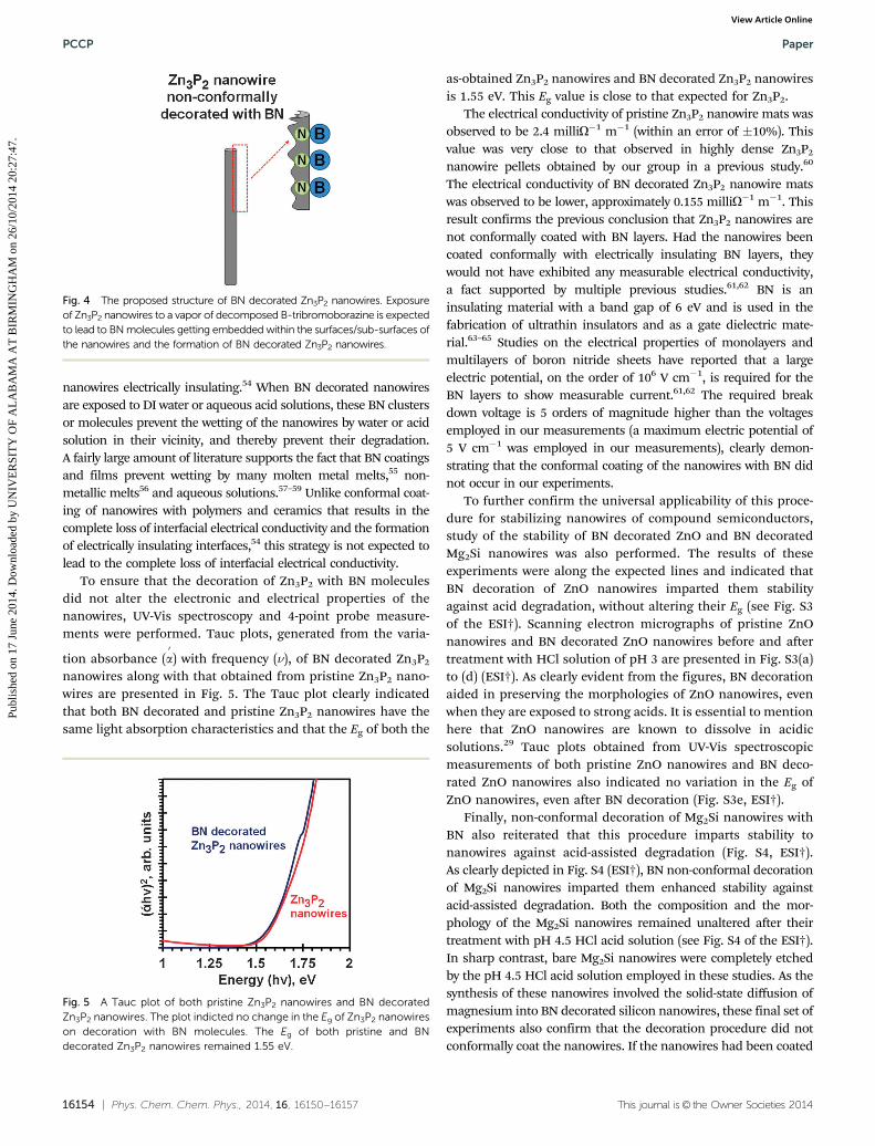
Overall, the analysis indicated that exposure of Zn3P2 nanowiresto decomposed B-tribromoborazine results in the formation ofnon-conformal, ultra-thin BN coating on the surfaces. It is postu-lated that this non-conformal, ultra-thin BN coating is composedof multiple BN nanocluster islands or BN individual molecules.These nanoclusters or molecules are physically embedded on thesurfaces/sub-surfaces of the nanowires (Fig. 4), and not chemicallybonded to the surfaces.50 It is believed that careful control of theamount of B-tribromoborazine allowed for the formation of suchnon-conformal BN surface decoration on nanowire surfaces. Hadsurplus amounts of B-tribromoborazine supplied, it would haveresulted in conformal coating of the nanowires with BN layers.However, such conformal coatings51–53 would have rendered the
Fig. 2 Scanning electron micrographs of BN decorated Zn3P2 nanowires(a) after they were treated with DI water and (b) HCl solution of pH 3. Thenanowires retained their morphologies in both the cases. (c) and (d) Scanningelectron micrographs of pristine Zn3P2 nanowires after treatment with DIwater and pH 3 HCl solution. Complete degradation of the pristine Zn3P2
nanowires was observed in both the cases. (e) XRD spectra of BN decoratedZn3P2 nanowires after they are treated with DI water and pH 3 HCl solution.In both the cases, the nanowires retained their a-Zn3P2 phase. Peaks corre-sponding to zinc foil substrate employed for the synthesis of nanowires areindicated with an * in the figure. (f) TEM micrograph of a BN decorated Zn3P2
nanowire after it was treated with pH 3 HCl solution. The analysis indicatedthat no change to either the morphology or the phase of the nanowireoccurred on acid treatment. SAED pattern in the inset clearly confirmed thea-Zn3P2 phase of the nanowire.
Fig. 3 FTIR spectrum of BN decorated Zn3P2 nanowires indicating thepresence of BN. For comparison, the FTIR spectrum of the decomposedB-tribromoborazine source is also included.
Paper PCCP
Publ
ishe
d on
17
June
201
4. D
ownl
oade
d by
UN
IVE
RSI
TY
OF
AL
AB
AM
A A
T B
IRM
ING
HA
M o
n 26
/10/
2014
20:
27:4
7.
View Article Online
16154 | Phys. Chem. Chem. Phys., 2014, 16, 16150--16157 This journal is© the Owner Societies 2014
nanowires electrically insulating.54 When BN decorated nanowiresare exposed to DI water or aqueous acid solutions, these BN clustersor molecules prevent the wetting of the nanowires by water or acidsolution in their vicinity, and thereby prevent their degradation.A fairly large amount of literature supports the fact that BN coatingsand films prevent wetting by many molten metal melts,55 non-metallic melts56 and aqueous solutions.57–59 Unlike conformal coat-ing of nanowires with polymers and ceramics that results in thecomplete loss of interfacial electrical conductivity and the formationof electrically insulating interfaces,54 this strategy is not expected tolead to the complete loss of interfacial electrical conductivity.
To ensure that the decoration of Zn3P2 with BN moleculesdid not alter the electronic and electrical properties of thenanowires, UV-Vis spectroscopy and 4-point probe measure-ments were performed. Tauc plots, generated from the varia-
tion absorbance (a0) with frequency (n), of BN decorated Zn3P2
nanowires along with that obtained from pristine Zn3P2 nano-wires are presented in Fig. 5. The Tauc plot clearly indicatedthat both BN decorated and pristine Zn3P2 nanowires have thesame light absorption characteristics and that the Eg of both the
as-obtained Zn3P2 nanowires and BN decorated Zn3P2 nanowiresis 1.55 eV. This Eg value is close to that expected for Zn3P2.
The electrical conductivity of pristine Zn3P2 nanowire mats wasobserved to be 2.4 milliO�1 m�1 (within an error of �10%). Thisvalue was very close to that observed in highly dense Zn3P2
nanowire pellets obtained by our group in a previous study.60
The electrical conductivity of BN decorated Zn3P2 nanowire matswas observed to be lower, approximately 0.155 milliO�1 m�1. Thisresult confirms the previous conclusion that Zn3P2 nanowires arenot conformally coated with BN layers. Had the nanowires beencoated conformally with electrically insulating BN layers, theywould not have exhibited any measurable electrical conductivity,a fact supported by multiple previous studies.61,62 BN is aninsulating material with a band gap of 6 eV and is used in thefabrication of ultrathin insulators and as a gate dielectric mate-rial.63–65 Studies on the electrical properties of monolayers andmultilayers of boron nitride sheets have reported that a largeelectric potential, on the order of 106 V cm�1, is required for theBN layers to show measurable current.61,62 The required breakdown voltage is 5 orders of magnitude higher than the voltagesemployed in our measurements (a maximum electric potential of5 V cm�1 was employed in our measurements), clearly demon-strating that the conformal coating of the nanowires with BN didnot occur in our experiments.
To further confirm the universal applicability of this proce-dure for stabilizing nanowires of compound semiconductors,study of the stability of BN decorated ZnO and BN decoratedMg2Si nanowires was also performed. The results of theseexperiments were along the expected lines and indicated thatBN decoration of ZnO nanowires imparted them stabilityagainst acid degradation, without altering their Eg (see Fig. S3of the ESI†). Scanning electron micrographs of pristine ZnOnanowires and BN decorated ZnO nanowires before and aftertreatment with HCl solution of pH 3 are presented in Fig. S3(a)to (d) (ESI†). As clearly evident from the figures, BN decorationaided in preserving the morphologies of ZnO nanowires, evenwhen they are exposed to strong acids. It is essential to mentionhere that ZnO nanowires are known to dissolve in acidicsolutions.29 Tauc plots obtained from UV-Vis spectroscopicmeasurements of both pristine ZnO nanowires and BN deco-rated ZnO nanowires also indicated no variation in the Eg ofZnO nanowires, even after BN decoration (Fig. S3e, ESI†).
Finally, non-conformal decoration of Mg2Si nanowires withBN also reiterated that this procedure imparts stability tonanowires against acid-assisted degradation (Fig. S4, ESI†).As clearly depicted in Fig. S4 (ESI†), BN non-conformal decorationof Mg2Si nanowires imparted them enhanced stability againstacid-assisted degradation. Both the composition and the mor-phology of the Mg2Si nanowires remained unaltered after theirtreatment with pH 4.5 HCl acid solution (see Fig. S4 of the ESI†).In sharp contrast, bare Mg2Si nanowires were completely etchedby the pH 4.5 HCl acid solution employed in these studies. As thesynthesis of these nanowires involved the solid-state diffusion ofmagnesium into BN decorated silicon nanowires, these final set ofexperiments also confirm that the decoration procedure did notconformally coat the nanowires. If the nanowires had been coated
Fig. 4 The proposed structure of BN decorated Zn3P2 nanowires. Exposureof Zn3P2 nanowires to a vapor of decomposed B-tribromoborazine is expectedto lead to BN molecules getting embedded within the surfaces/sub-surfaces ofthe nanowires and the formation of BN decorated Zn3P2 nanowires.
Fig. 5 A Tauc plot of both pristine Zn3P2 nanowires and BN decoratedZn3P2 nanowires. The plot indicted no change in the Eg of Zn3P2 nanowireson decoration with BN molecules. The Eg of both pristine and BNdecorated Zn3P2 nanowires remained 1.55 eV.
PCCP Paper
Publ
ishe
d on
17
June
201
4. D
ownl
oade
d by
UN
IVE
RSI
TY
OF
AL
AB
AM
A A
T B
IRM
ING
HA
M o
n 26
/10/
2014
20:
27:4
7.
View Article Online
This journal is© the Owner Societies 2014 Phys. Chem. Chem. Phys., 2014, 16, 16150--16157 | 16155
with either a complete monolayer or multilayers of BN, thenmagnesium would not have diffused into the nanowires and thiswould have prevented the formation of Mg2Si nanowires.46
Conclusions
To summarize, a novel strategy for stabilizing the surfacesof compound semiconductors is presented. This strategyprimarily involved the use of the non-conformal decoration of thesurfaces of compound semiconductor nanowires with small inor-ganic molecules of BN, experimentally accomplished by exposingZn3P2 and ZnO nanowires to a vapor of decomposed B-tribromo-borazine in situ in a chemical vapor deposition (CVD) chamberimmediately after their synthesis. By controlling the amount ofB-tribromoborazine employed for this purpose, conformal BN coat-ing of the nanowires is prevented. For the synthesis of Mg2Sinanowires non-conformally decorated with BN molecules, a slightlyalternate procedure was employed. Here, BN surface decoratedsilicon nanowires were phase transformed into BN surface deco-rated Mg2Si nanowires. It is hypothesized that the decorationprocess is expected to embed BN molecules within the surfaces/sub-surfaces of the nanowires. These molecules are expected toprevent the wetting of the surfaces by either water or aqueous acidicsolutions and hence prevent their degradation. The decorationprocess did not majorly alter the electronic properties of thenanowires. UV-Vis measurements of the nanowires before and afterBN decoration clearly indicated no change in the Eg of Zn3P2 andZnO nanowires. 4-Point probe electrical conductivity measurementsof the nanowires indicated that the stabilization procedure allowedfor retaining the electrical conductivity between nanowires whenassembled, and confirmed the earlier conclusion that the procedureemployed did not result in nanowires conformally coated with BNlayers. This novel method of stabilizing nanowires, along with ourrecent reports on the strategies for the large-scale synthesis andassembly of nanowires, is expected to be of huge importance in theenergy conversion device fabrication field as the instability ofcompound semiconductor nanowires is a major deterrent to theirwidespread use in the fabrication of the above-mentioned devices.
Acknowledgements
The authors acknowledge financial support from the NSF/DOEthermoelectrics partnership program (NSF CBET grant # 1048702).Access provided to the materials characterization facilities housedinside the Conn Center for Renewable Energy at the University ofLouisville is gratefully acknowledged.
References
1 V. C. Holmberg and B. A. Korgel, Corrosion Resistance ofThiol- and Alkene-Passivated Germanium Nanowires, Chem.Mater., 2010, 22, 3698–3703.
2 H. Adhikari, P. C. McIntyre, S. Sun, P. Pianetta and C. E.Chidsey, Photoemission studies of passivation of germa-nium nanowires, Appl. Phys. Lett., 2005, 87, 263109.
3 M. Y. Bashouti, T. Stelzner, A. Berger, S. Christiansen andH. Haick, Chemical Passivation of Silicon Nanowires withC1–C6 Alkyl Chains through Covalent Si–C Bonds, J. Phys.Chem. C, 2008, 112, 19168–19172.
4 A. S. Arico, P. Bruce, B. Scrosati, J.-M. Tarascon and W. VanSchalkwijk, Nanostructured materials for advanced energyconversion and storage devices, Nat. Mater., 2005, 4, 366–377.
5 G. Cao, Nanostructures and nanomaterials, Imperial CollegePress, 2004.
6 C. N. R. Rao, A. Muller and A. K. Cheetham, The chemistry ofnanomaterials, Wiley, 2006, vol. 1.
7 D. Wang, Y.-L. Chang, Z. Liu and H. Dai, Oxidation resistantgermanium nanowires: bulk synthesis, long chain alka-nethiol functionalization, and Langmuir-Blodgett assembly,J. Am. Chem. Soc., 2005, 127, 11871–11875.
8 T. Hanrath and B. A. Korgel, Chemical Surface Passivationof Ge Nanowires, J. Am. Chem. Soc., 2004, 126, 15466–15472.
9 G. M. Kimball, J. P. Bosco, A. M. Muller, S. F. Tajdar,B. S. Brunschwig, H. A. Atwater and N. S. Lewis, Passivationof Zn3P2 substrates by aqueous chemical etching and airoxidation, J. Appl. Phys., 2012, 112, 106101.
10 P. Nayar and A. Catalano, Zinc phosphide-zinc oxide hetero-junction solar cells, Appl. Phys. Lett., 1981, 39, 105–107.
11 A. Yaroshevsky, Abundances of chemical elements in theEarth’s crust, Geochem. Int., 2006, 44, 48–55.
12 K. Chopra, P. Paulson and V. Dutta, Thin-film solar cells: anoverview, Prog. Photovoltaics, 2004, 12, 69–92.
13 M. Bhushan and A. Catalano, Polycrystalline Zn3P2 Schottkybarrier solar cells, Appl. Phys. Lett., 1981, 38, 39–41.
14 J. Misiewicz, Minority-carrier diffusion length in Zn3P2,Phys. Status Solidi A, 1981, 65, K95–K97.
15 N. Wyeth and A. Catalano, Spectral response measurementsof minority-carrier diffusion length in Zn 3 P 2, J. Appl. Phys.,1979, 50, 1403–1407.
16 C. Eason, J. Ross, H. Blackie and A. Fairweather, Toxicologyand ecotoxicology of zinc phosphide as used for pest controlin New Zealand, N. Z. J. Ecol., 2013, 37, 1–11.
17 L. Brockway, M. Van Laer, Y. Kang and S. Vaddiraju,Large-scale synthesis and in situ functionalization ofZn3P2 and Zn4Sb3 nanowire powders, Phys. Chem. Chem.Phys., 2013, 15, 6260–6267.
18 J. Greenberg, V. Lazarev, S. Kozlov and V. Shevchenko,The sublimation thermodynamics of Zn3P2, J. Chem. Ther-modyn., 1974, 6, 1005–1012.
19 F.-C. Wang, R. H. Bube, R. S. Feigelson and R. K. Route,Single crystal growth of Zn3P2, J. Cryst. Growth, 1981, 55,268–272.
20 H. Yin, M. Christensen, B. Pedersen, E. Nishibori, S. Aoyagiand B. B. Iversen, Thermal Stability of ThermoelectricZn4Sb3, J. Electron. Mater., 2010, 39, 1957–1959.
21 S. Schlecht, C. Erk and M. Yosef, Nanoscale zinc anti-monides: synthesis and phase stability, Inorg. Chem., 2006,45, 1693–1697.
22 K. Koumoto, Y. Wang, R. Zhang, A. Kosuga andR. Funahashi, Oxide thermoelectric materials: a nanostruc-turing approach, Annu. Rev. Mater. Res., 2010, 40, 363–394.
Paper PCCP
Publ
ishe
d on
17
June
201
4. D
ownl
oade
d by
UN
IVE
RSI
TY
OF
AL
AB
AM
A A
T B
IRM
ING
HA
M o
n 26
/10/
2014
20:
27:4
7.
View Article Online
16156 | Phys. Chem. Chem. Phys., 2014, 16, 16150--16157 This journal is© the Owner Societies 2014
23 V. Srikant and D. R. Clarke, On the optical band gap of zincoxide, J. Appl. Phys., 1998, 83, 5447–5451.
24 A. Tsukazaki, A. Ohtomo, T. Onuma, M. Ohtani, T. Makino,M. Sumiya, K. Ohtani, S. F. Chichibu, S. Fuke and Y. Segawa,Repeated temperature modulation epitaxy for p-type dopingand light-emitting diode based on ZnO, Nat. Mater., 2004, 4,42–46.
25 W. H. Horsthuis, ZnO processing for integrated opticsensors, Thin Solid Films, 1986, 137, 185–192.
26 M. Willander, O. Nur, Q. Zhao, L. Yang, M. Lorenz, B. Cao,J. Z. Perez, C. Czekalla, G. Zimmermann and M. Grundmann,Zinc oxide nanorod based photonic devices: recent progressin growth light emitting diodes and lasers, Nanotechnology,2009, 20, 332001.
27 C.-P. Lee, C.-Y. Chou, C.-Y. Chen, M.-H. Yeh, L.-Y. Lin,R. Vittal, C.-G. Wu and K.-C. Ho, Zinc oxide-based dye-sensitized solar cells with a ruthenium dye containing analkyl bithiophene group, J. Power Sources, 2013, 1–9.
28 N. Nesakumar, K. Thandavan, S. Sethuraman, U. M. Krishnanand J. B. B. Rayappan, An electrochemical biosensor withnanointerface for lactate detection based on lactate dehydro-genase immobilized on zinc oxide nanorods, J. Colloid Inter-face Sci., 2014, 414, 90–96.
29 K. Eda, A. Iga and M. Matsuoka, Degradation mechanism of non-Ohmic zinc oxide ceramics, J. Appl. Phys., 1980, 51, 2678–2684.
30 S. K. Bux, M. T. Yeung, E. S. Toberer, G. J. Snyder, R. B.Kaner and J.-P. Fleurial, Mechanochemical synthesis andthermoelectric properties of high quality magnesium silicide,J. Mater. Chem., 2011, 21, 12259–12266.
31 J.-Y. Jung and I.-H. Kim, Synthesis and thermoelectricproperties of n-Type Mg2Si, Electron. Mater. Lett., 2010, 6,187–191.
32 J.-Y. Jung, K.-H. Park, I.-H. Kim, Thermoelectric Propertiesof Sb-doped Mg2Si Prepared by Solid-State Synthesis, IOPConference Series: Materials Science and Engineering,2011, IOP Publishing, p. 142006.
33 J.-i. Tani and H. Kido, Thermoelectric properties ofBi-doped Mg2Si semiconductors, Phys. B, 2005, 364, 218–224.
34 R. Escalera-Lozano, C. A. Gutierrez-Chavarrıa, M. A. Pech-Canul and M. I. Pech-Canul, Degradation of Al/SiCp Compo-sites Processed with Fly Ash via Reactive Infiltration, MaterialsScience Forum, Trans Tech Publ, 2007, pp. 139–144.
35 B. Hidding, M. Pfitzner, D. Simone and C. Bruno, Reviewof the potential of silanes as rocket/scramjet fuels,Acta Astronaut., 2008, 63, 379–388.
36 K. Adlkofer, W. Eck, M. Grunze and M. Tanaka, Surfaceengineering of gallium arsenide with 4-mercaptobiphenylmonolayers, J. Phys. Chem. B, 2003, 107, 587–591.
37 N. Myung, Y. Bae and A. J. Bard, Effect of surface passivationon the electrogenerated chemiluminescence of CdSe/ZnSenanocrystals, Nano Lett., 2003, 3, 1053–1055.
38 X.-S. Wang, T. E. Dykstra, M. R. Salvador, I. Manners, G. D.Scholes and M. A. Winnik, Surface passivation of lumines-cent colloidal quantum dots with poly (dimethylaminoethylmethacrylate) through a ligand exchange process, J. Am.Chem. Soc., 2004, 126, 7784–7785.
39 V. C. Holmberg, M. R. Rasch and B. A. Korgel, PEGylation ofCarboxylic Acid-Functionalized Germanium Nanowires,Langmuir, 2010, 26, 14241–14246.
40 H. Jenny, S. Gessel and F. Bingham, Comparative study ofdecomposition rates of organic matter in temperate andtropical regions, J. Soil Sci., 1949, 68, 419–432.
41 K. Tennakone, S. Wickramanayake, P. Samarasekara andC. Fernando, Doping of semiconductor particles with salts,Phys. Status Solidi A, 1987, 104, K57–K60.
42 I. V. Kazakov and A. Y. Timoshkin, Vaporization andthermal decomposition of B,B0,B00-tribromoborazine, Russ.J. Inorg. Chem., 2012, 57, 557–563.
43 A. B. Murphy, Band-gap determination from diffuse reflec-tance measurements of semiconductor films, and applica-tion to photoelectrochemical water-splitting, Sol. EnergyMater. Sol. Cells, 2007, 91, 1326–1337.
44 S. Bhattacharya, D. Banerjee, K. W. Adu, S. Samui andS. Bhattacharyya, Confinement in silicon nanowires: opticalproperties, Appl. Phys. Lett., 2004, 85, 2008–2010.
45 Y. Kang, L. Brockway and S. Vaddiraju, A simple phasetransformation strategy for converting silicon nanowiresinto metal silicide nanowires: magnesium silicide, Mater.Lett., 2013, 100, 106–110.
46 Y. Kang and S. Vaddiraju, Solid-State Phase Transformationas a Route for the Simultaneous Synthesis and Welding ofSingle-Crystalline Mg2Si Nanowires, Chem. Mater., 2014, 26,2814–2819.
47 S. Reich, A. Ferrari, R. Arenal, A. Loiseau, I. Bello andJ. Robertson, Resonant Raman scattering in cubic andhexagonal boron nitride, Phys. Rev. B: Condens. MatterMater. Phys., 2005, 71, 205201.
48 K.-L. Barth, A. Lunk and J. Ulmer, Influence of the deposi-tion parameters on boron nitride growth mechanisms in ahollow cathode arc evaporation device, Surf. Coat. Technol.,1997, 92, 96–103.
49 L. Yu, B. Gao, Z. Chen, C. Sun, D. Cui, C. Wang, Q. Wangand M. Jiang, In situ FTIR investigation on phase trans-formations in BN nanoparticles, Chin. Sci. Bull., 2005, 50,2827–2831.
50 N.-M. Park, C.-J. Choi, T.-Y. Seong and S.-J. Park, QuantumConfinement in Amorphous Silicon Quantum Dots Embeddedin Silicon Nitride, Phys. Rev. Lett., 2001, 86, 1355–1357.
51 C. Tang, Y. Bando, T. Sato, K. Kurashima, X. Ding, Z. Ganand S. Qi, SiC and its bicrystalline nanowires with uniformBN coatings, Appl. Phys. Lett., 2002, 80, 4641–4643.
52 C. Tang, Y. Bando, T. Sato and K. Kurashima, Uniformboron nitride coatings on silicon carbide nanowires, Adv.Mater., 2002, 14, 1046–1049.
53 C. Tang, Y. Bando, D. Golberg, X. Ding and S. Qi, Boronnitride nanotubes filled with Ni and NiSi2 nanowiresin situ, J. Phys. Chem. B, 2003, 107, 6539–6543.
54 W.-Q. Han and A. Zettl, GaN nanorods coated with pure BN,Appl. Phys. Lett., 2002, 81, 5051–5053.
55 O. Dezellus and N. Eustathopoulos, Fundamental issues ofreactive wetting by liquid metals, J. Mater. Sci., 2010, 45,4256–4264.
PCCP Paper
Publ
ishe
d on
17
June
201
4. D
ownl
oade
d by
UN
IVE
RSI
TY
OF
AL
AB
AM
A A
T B
IRM
ING
HA
M o
n 26
/10/
2014
20:
27:4
7.
View Article Online
This journal is© the Owner Societies 2014 Phys. Chem. Chem. Phys., 2014, 16, 16150--16157 | 16157
56 L. H. Li and Y. Chen, Superhydrophobic Properties ofNonaligned Boron Nitride Nanotube Films, Langmuir,2009, 26, 5135–5140.
57 O. D. Collins III, Boron nitride incorporated in polymerproducts, US Pat., 3,261,800A, 1966.
58 D. Golberg, F.-F. Xu and Y. Bando, Filling boron nitridenanotubes with metals, Appl. Phys. A: Mater. Sci. Process.,2003, 76, 479–485.
59 H. Fujii, H. Nakae and K. Okada, Interfacial reaction wettingin the boron nitride/molten aluminum system, Acta Metall.Mater., 1993, 41, 2963–2971.
60 B. Lance, V. Venkata, A.-A. Hasti, S.-Y. Reza and V. Sreeram,Thermoelectric properties of large-scale Zn 3 P 2 nanowireassemblies, Nanotechnology, 2014, 25, 145401.
61 L. Britnell, R. V. Gorbachev, R. Jalil, B. D. Belle, F. Schedin,M. I. Katsnelson, L. Eaves, S. V. Morozov, A. S. Mayorov,N. M. R. Peres, C. A. H. Neto, J. Leist, A. K. Geim, L. A.
Ponomarenko and K. S. Novoselov, Electron Tunnelingthrough Ultrathin Boron Nitride Crystalline Barriers, NanoLett., 2012, 12, 1707–1710.
62 G.-H. Lee, Y.-J. Yu, C. Lee, C. Dean, K. L. Shepard, P. Kim andJ. Hone, Electron tunneling through atomically flat and ultrathinhexagonal boron nitride, Appl. Phys. Lett., 2011, 99, 243114.
63 C. Dean, A. Young, I. Meric, C. Lee, L. Wang, S. Sorgenfrei,K. Watanabe, T. Taniguchi, P. Kim and K. Shepard, Boronnitride substrates for high-quality graphene electronics,Nat. Nanotechnol., 2010, 5, 722–726.
64 M. Radosavljevic, J. Appenzeller, V. Derycke, R. Martel,P. Avouris, A. Loiseau, J.-L. Cochon and D. Pigache, Elec-trical properties and transport in boron nitride nanotubes,Appl. Phys. Lett., 2003, 82, 4131–4133.
65 O. Chuhei and N. Ayato, Ultra-thin epitaxial films ofgraphite and hexagonal boron nitride on solid surfaces,J. Phys.: Condens. Matter, 1997, 9, 1–20.
Paper PCCP
Publ
ishe
d on
17
June
201
4. D
ownl
oade
d by
UN
IVE
RSI
TY
OF
AL
AB
AM
A A
T B
IRM
ING
HA
M o
n 26
/10/
2014
20:
27:4
7.
View Article Online