Embed Size (px)
Citation preview

Non-Destructive Test MethodsFailure analysis (FA), by its very nature, is needed only when things goawry. Before any testing is performed on the sample, a decision mustbe made as to whether or not the sample is allowed to be destroyedin the process of testing. Non-destructive testing can allow for re-useof the assembly since the functionality is not altered, but there stillremains the possibility that inadvertent damage can occur throughthe course of the analysis. If non-destructive testing is preferred, thenthe following types of analysis can be performed. The testing can bedivided into four categories: visual, X-ray (X-ray imaging and X-rayfluorescence), cleanliness (resistivity of solvent extract, ionchromatography, and Fourier transform infrared spectroscopy), andmechanical (non-destructive wire bond pull).
Visual Examination
Optical Microscopy with Digital Imaging
Optical microscopy and photography provide a permanent visualrecord of the sample, from the point of arrival to the laboratory througheach step along the way in the determination of the root cause of thefailure. A stereo microscope is used in optical microscopy to give good
Figure 1: Image of a dendrite growing between two pins causing a short.
depth of field when the sample is placed directly underneath the mainlens. When used with calibration grids and the appropriate software,images can be captured with scale bars and measurements offeatures, at magnifications ranging from 7x to 90x.
Figure 1 shows a case where salt was deposited on an unprotectedportion of an assembly and with the addition of high humidity andelectrical bias; a dendrite grew between two adjacent conductors andcaused an electrical short. This failure was due to exposure to acorrosive environment without adequate conformal coating protection.
Figure 2 shows a partial fingerprint on the assembly, underneath theconformal coating. The oils from the finger print contributed to thepoor adhesion of the coating, which in turn led to the dendrite seen inFigure 1.
Figure 2: The oils from this fingerprint contributed to poor adhesion ofthe conformal coating and led to the corrosion seen in Figure 1.
Optical Inspection System
An optical inspection system is similar to optical microscopy exceptthe lens is placed very close to the board, nearly touching it, and amirror directs the light path 90°, so that features to the right (or left)
continued on next page

of the lens can be viewed. Fine features underneath components canbe observed, especially the first two to five rows of a ball grid array(BGA) component. The row depth is dependent on the lighting andspace beneath the component. The goal is to see if the solder ballshave collapsed properly after undergoing the reflow process and if anyabnormalities exist, such as contamination or materials bridging leads.
Figure 3 shows a slight misalignment of a row of solder balls. This isacceptable per IPC A-610 Revision D since the BGA solder balls didnot violate the minimum electrical clearance. However, it is a processindicator of a potential issue in the manufacturing process due toeither manual placement of the BGA or an alignment issue in the pick-and-place system.
Figure 3: Image of a slight misalignment of a row of solder balls. This isa process indicator that either the manual placement or the pick-and-place system was slightly off.
Automated Optical Inspection
Automated optical inspection (AOI) is used as a process tool forinspection of bare boards, solder paste deposition, componentplacement prior to reflow, post-reflow component conditions, solderjoints, and surface anomalies on assemblies. By programming thefeatures of a good board assembly, comparisons with subsequentassemblies can determine if they pass or fail.
X-Ray Examination
X-Ray Fluorescence (XRF)
XRF is used to identify composition and plating thickness for elementsranging from titanium (Ti, element 22) to uranium (U, element 92). Bybombarding a sample with high energy X-rays, “secondary” (orfluorescent) X-rays can be emitted which are characteristic of theatoms present in the sample. Figure 4 shows an XRF spectrum that isindicative of an electroless nickel immersion gold (ENIG) surface finishover copper. Figure 5 shows an XRF spectrum for solder jointcomposed of tin-lead solder.
X-Ray Inspection
X-ray inspection is used to visualize assemblies by observingdifferences in density and composition. The denser an item, the darkerit appears in the image. Some of the features that can be observed
are: cracks, solder joints, traces, vias, voiding within solder joints, andwire bonds. Figure 6 shows a BGA component, where several groupsof solder balls have bridged during the reflow process due to solderpaste deposition and the thermal profile.
Figure 4: XRF spectrum of an electroless nickel immersion gold (ENIG)surface finish over copper, where copper (Cu), gold (Au), and nickel (Ni)were observed.
Figure 5: XRF spectrum of a tin-lead solder joint, where lead (Pb) andtin (Sn) were observed.
Figure 6: X-ray image of a BGA component with bridging solder balls.
continued on next page
Cleanliness Examination
To determine if there are ionic contaminants present on the boardassembly, there are two methods that give different levels ofinformation: bulk ionics testing and ion chromatography. To determineif there are organic contaminants present on the assembly, Fouriertransform infrared spectroscopy can be performed. A spectrum isobtained showing peak location and height which indicate whatchemical functional groups (alcohol, epoxy, siloxanes) are present.
Bulk Ionics Testing
The more general method follows IPC-TM-650 2.3.25C, Detection andMeasurement of Ionizable Surface Contaminants by Resistivity ofSolvent Extract (ROSE) [1], in which a sample is immersed in anisothermal bath (at 35ºC) containing a 3 to 1 solution of isopropylalcohol to deionized water. Ionic contaminants extracted from thesample pass through a conductivity cell which continuously measuresthe conductivity of the solution. The conductivity values are integratedover the time of the extraction. The ionic material then passes througha deionization column before being recirculated back into the testchamber. As the ionic materials are extracted from the assemblies,the conductivity (and hence resistivity) of the solution will changedynamically until nearly all of the extractable ionic material has been removed.
Results from dynamic extraction by Ionograph are reported inmicrograms of sodium chloride (NaCl) equivalent per square inch. Forassemblies soldered using rosin based fluxes, the ionic cleanlinessrequirement per J-STD-001D is a maximum of 10.06 µg NaClequivalent/in2 (1.56 µg NaCl equivalent/cm2). There is no industrystandard for acceptable bulk ionic levels, but it is better to have as lowa value as possible. The EMPF recommends Ionograph results to notexceed a level of 2 to 3 µg NaCl equivalent/in2.
Ion Chromatography
The more specific method of ionic contaminant analysis is IPC-TM-650 2.3.28A, Ionic Analysis of Circuit Boards, Ion ChromatographyMethod [2], in which the samples are sealed in a Kapak bag with a 3to 1 solution of isopropyl alcohol to water and heated in an 80 °Cwater bath for 1 hour to extract any ionic residues. The extract solutionis analyzed against known standards to confirm the presence of andquantify each of the following anions: fluoride, chloride, bromide,nitrate, phosphate, and sulfate in units of µg/mL. The surface area iscalculated from the board dimensions and the final results arereported in µg/in2.
ACI’s maximum recommended amounts of fluoride, chloride, bromide,nitrate, and sulfate for bare boards are 2, 4, 5, 1, and 3 µg/in2,respectively. The recommended levels of ionic contamination for
populated assemblies will depend upon the application. However, fortypical component packages on FR-4 or a like substrate, the maximumrecommended amounts of fluoride, chloride, bromide, nitrate, andsulfate are 2, 9, 15, 1 and 10 µg/in2, respectively. Both sets ofacceptance criteria were developed from experience and inconjunction with industry leaders.
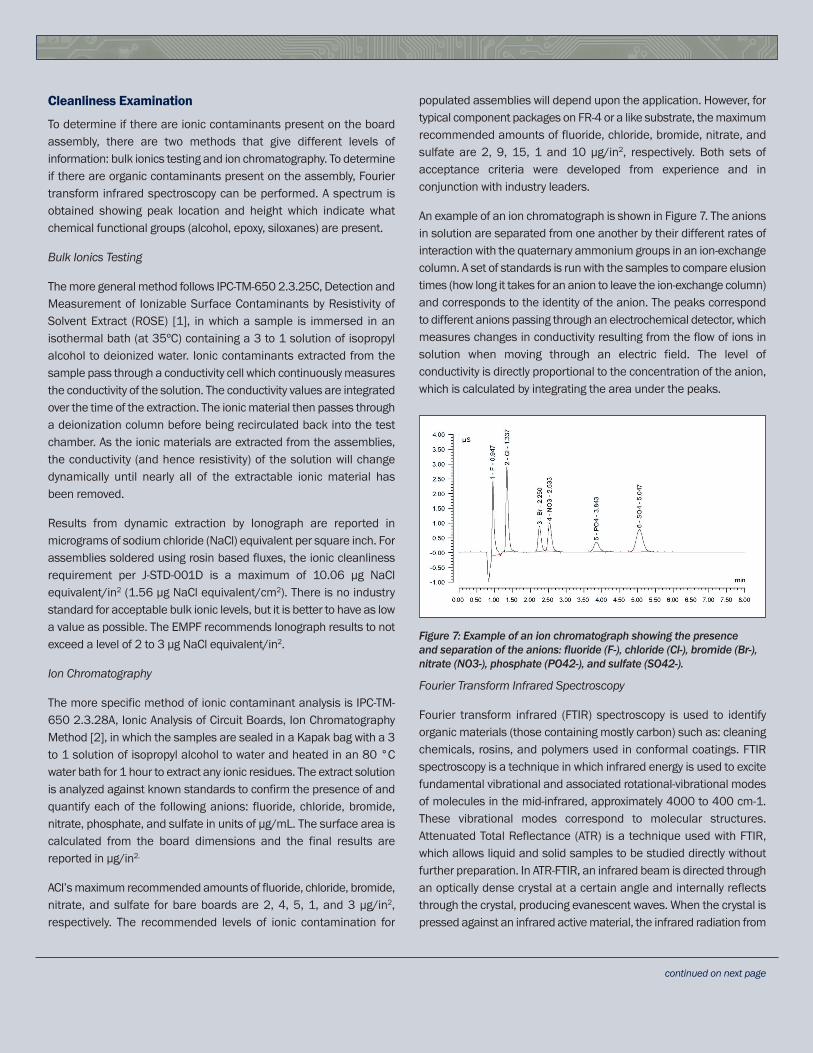
An example of an ion chromatograph is shown in Figure 7. The anionsin solution are separated from one another by their different rates ofinteraction with the quaternary ammonium groups in an ion-exchangecolumn. A set of standards is run with the samples to compare elusiontimes (how long it takes for an anion to leave the ion-exchange column)and corresponds to the identity of the anion. The peaks correspondto different anions passing through an electrochemical detector, whichmeasures changes in conductivity resulting from the flow of ions insolution when moving through an electric field. The level ofconductivity is directly proportional to the concentration of the anion,which is calculated by integrating the area under the peaks.
Figure 7: Example of an ion chromatograph showing the presence and separation of the anions: fluoride (F-), chloride (Cl-), bromide (Br-),nitrate (NO3-), phosphate (PO42-), and sulfate (SO42-).
Fourier Transform Infrared Spectroscopy
Fourier transform infrared (FTIR) spectroscopy is used to identifyorganic materials (those containing mostly carbon) such as: cleaningchemicals, rosins, and polymers used in conformal coatings. FTIRspectroscopy is a technique in which infrared energy is used to excitefundamental vibrational and associated rotational-vibrational modesof molecules in the mid-infrared, approximately 4000 to 400 cm-1.These vibrational modes correspond to molecular structures.Attenuated Total Reflectance (ATR) is a technique used with FTIR,which allows liquid and solid samples to be studied directly withoutfurther preparation. In ATR-FTIR, an infrared beam is directed throughan optically dense crystal at a certain angle and internally reflectsthrough the crystal, producing evanescent waves. When the crystal ispressed against an infrared active material, the infrared radiation from
continued on next page

ACI Technologies, Inc. 1 International Plaza, Suite 600 Philadelphia, PA 19113 phone: 610.362.1200 web: www.aciusa.org
Training Center phone: 610.362.1295 email: [email protected]
Helpline phone: 610.362.1320 email: [email protected]
the evanescent waves penetrates typically one to four micrometersinto the sample.
Figure 8 shows an FTIR spectrum of an unknown residue rinsed off aboard assembly compared to that of a known adhesive compound.The residue was contributing to the poor adhesion of a conformalcoating to this assembly.
Figure 8: FTIR spectra for an unknown residue from a board assembly(top, red) compared to a known adhesive compound (bottom, blue).
Mechanical Examination
Non-Destructive Wire Bond Pull Test
Method 2023.5 of MIL-STD-883 [3] provides for a Non-DestructiveBond Pull, where an applied stress (measured in grams force (gf) pull)is used to reveal non-acceptable wire bonds while avoiding damageto acceptable wire bonds in a package. This test is intended for “ClassS” parts or parts intended for use in the high reliability space flightcommunity [4]. Any bond failures are unacceptable, but based on theprogram requirements, rework and retest may be acceptable. Table 1lists the pull forces for a set of standard wire sizes.
Table 1: Non-destructive pull forces.
There are conditions for which this test may not be applicable, suchas having a high pin count of 84 or more external terminations andsmall bonding wire pitch at the package post of less than or equal to12 mils (304.8 µm). Alternative procedures are given to evaluate thewire bonds, such as: review of manufacture quality records and rawmaterial control, a thermal mechanical analysis of the package andthe bonds over time and with temperature cycling, and a 100% visualinspection of all bonds. For packages with gold plated posts, a baketest at 300°C for one hour in air or inert atmosphere is performed totest for contamination anomalies in the plating. This bake test callsfor 45 bond pulls to destruction per method 2011 of MIL-STD-883 andfalls into the realm of destructive testing.
Summary
Non-destructive testing can provide valuable information as to the rootcause of failures that can occur in electronics manufacturing. The ACITechnologies facilities are well equipped to assist with non-destructivetesting using all of these techniques, along with the skilled staff toprovide interpretation of the data, and provide the appropriaterecommendations to remedy the conditions leading to failure.
References
[1] “Detection and Measurement of Ionizable Surface Contaminantsby Resistivity of Solvent Extract - 2/01.” IPC-TM-650 2.3.25C.<http://www.ipc.org/4.0_Knowledge/4.1_Standards/test/2-3_2-3-25c.pdf>
[2] “Ionic Analysis of Circuit Boards, Ion Chromatography Method -5/04.” IPC-TM-650 2.3.28A. <http://www.ipc.org/4.0_Knowledge/4.1_Standards/test/2.3.28A.pdf>
[3] Test Method Standards, Microcircuits.” MIL-STD-883. <http://www.dscc.dla.mil/Programs/MilSpec/listdocs.asp?BasicDoc=MIL-STD-883>
[4] “Assurance Issues Related to Electronic Wire Bonds.” NASAGoddard Space Flight Center. <http://nepp.nasa.gov/wirebond/>
ACI Technologies, Inc.