Embed Size (px)
Citation preview

Silicon PhotonicsSilicon-based micro and nanophotonic devices
http://silicon-photonics.ief.u-psud.fr/
Laurent Vivien
Pedro Damas, Xavier Le Roux, Eric Cassan, Delphine Marris-Morini,
Nicolas Izard, Alain Bosseboeuf, Thomas Maroutian, Philippe Lecoeur
Institut d’Electronique Fondamentale, CNRS UMR 8622,
Université Paris Sud, 91405 Orsay Cedex, France
http://silicon-photonics.ief.u-psud.fr/
Nonlinear optics in silicon:overview and future developments
http://silicon-photonics.ief.u-psud.fr/
Outline
� Motivation
� Nonlinear optics in silicon
� χ(3) in silicon� χ(2) in silicon
� Strained silicon photonics
� Conclusions

http://silicon-photonics.ief.u-psud.fr/
Global internet traffic
3
Source: L.Oxenlowe, Denmark Courtesy: D. Moss, CUDOS, Australia

http://silicon-photonics.ief.u-psud.fr/
Advanced video technology
4
3D displays High Dynamic range
Future: Ultra high definition (4320p, 30bpp, 60Hz) needs 60 Gbps !

http://silicon-photonics.ief.u-psud.fr/
Power consumption
5
Source: Shu Namiki, Japan Courtesy: D. Moss, CUDOS, Australia
http://silicon-photonics.ief.u-psud.fr/
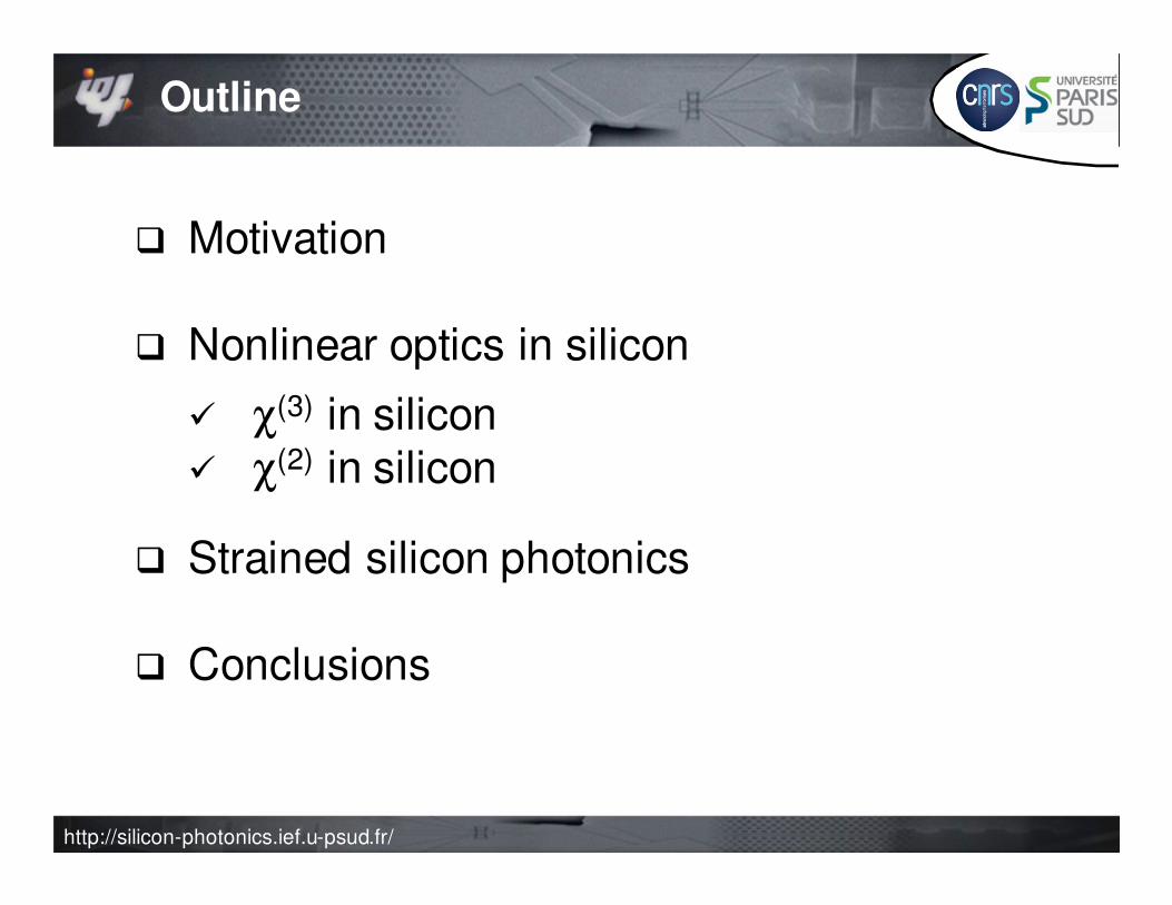
Data centers
6
Source: L.Oxenlowe, Denmark Courtesy: D. Moss, CUDOS, Australia
Development of silicon photonics

http://silicon-photonics.ief.u-psud.fr/
Silicon photonic building blocks
7
Tunable III-V laser on Si
Laser Modulator Detector
Emitter Receiver
-80
-70
-60
-50
-40
-30
-20
-10
0
1 520 1 530 15 40 15 50 15 60 157 0 158 0
Po
we
r (
dB
m)
Wave length (n m)
40Gbt/s Silicon modulator
40Gbit/s Germanium photodetector

http://silicon-photonics.ief.u-psud.fr/
Photonic – Electronic circuits
8
Silicon
PhotonicsCMOS Analog
& Digital Circuits+
=
Laser Beam splitter
detector
modulator
Electronic Photonic
Integrated circuit
Sourc
e: L
uxte
ra
Main challenges:
� Faster� Driving voltage of modulator� Power consumption
And also� Integration cost � Packaging
All-optical signal processing and low power consumption
EO modulators based on nonlinear properties in silicon

http://silicon-photonics.ief.u-psud.fr/
Why silicon waveguide?
9
� High refractive index contrast between SiO2 (n~1.5) and Si (n~3.5)
� Strong light confinement of the guided mode (<0.1µm²)
� Si transparency in the near IR
� Lossless light propagation
� Dispersion can be engineered
400 nm
220 nm
SiO2
Si

http://silicon-photonics.ief.u-psud.fr/
Nonlinear optics in silicon
10
Nonlinear Polarization:
√ Pockels effect:
�Linear electro-optic effect
√ Wavelength conversion
� Second Harmonic Generation (SHG)
√ Kerr effect:
�Nonlinear electro-optic effect
√ Wavelength conversion
�Four wave mixing (FWM)
>>

http://silicon-photonics.ief.u-psud.fr/
Main drawback
11
� Two photon absorption process leading to free carrier absorption� Excess loss at high power reducing nonlinear efficiency
Silicon FOM= 0.3 in telecom band
FOM >> 1 to be efficient in nonlinear regime
Courtesy: D. Moss, CUDOS, Australia

http://silicon-photonics.ief.u-psud.fr/
FWM amplification in NIR
12
First observation of broadband gain in Si
Foster et al., Nature 441, 960 (2006).
To overcome this limitation:
� Sweep the photogenerated carriers out
� Reverse bias pin diode
�Mode confinement engineering
� Slot waveguides
�Mid-IR photonics
� Wavelength larger than 2.2µm
�Silicon nitride (Si3N4) photonics
�Wider gap energy (TPA negligible)

http://silicon-photonics.ief.u-psud.fr/
Towards Mid-IR wavelength range
13

http://silicon-photonics.ief.u-psud.fr/
Silicon nitride photonics
14

http://silicon-photonics.ief.u-psud.fr/
Outline
� Motivation
� Nonlinear optics in silicon
� χ(3) in silicon� χ(2) in silicon
� Strained silicon photonics
� Conclusions

http://silicon-photonics.ief.u-psud.fr/
Nonlinear optics in silicon
16
Nonlinear Polarization:
√ Pockels effect:
�Linear electro-optic effect
√ Wavelength conversion
� Second Harmonic Generation (SHG)
Break the symmetry of silicon crystal
Strained silicon
photonics
Without straining layer
With straining layer

http://silicon-photonics.ief.u-psud.fr/
χ(2) demonstration: State of the art
17
� No EO effect
� Ridge waveguides did not work
� Comp. strain:
√
� Tensile strain:
√
� Comp. strain:
√
� Huge enhancement of EO effect
� Tensile strain:√
� SiO2 layer:
√ 0.3 GPa
√ 1.2 – 1.5 um
√ Compressive or tensile strain
*All χ2 units are in pm/V
� SiN layer:
√ 1.0 GPa
√ 0.75 um
√ Compressive strain
Jacobsen et al. Nature 441, 199-202 (11 May 2006)

http://silicon-photonics.ief.u-psud.fr/
χ(2) demonstration: State of the art
18
� No EO effect
� Ridge waveguides did not work
� Comp. strain:
√
� Tensile strain:
√
� Comp. strain:
√
� Huge enhancement of EO effect
� Tensile strain:√
� SiO2 layer:
√ 0.3 GPa
√ 1.2 – 1.5 um
√ Compressive or tensile strain
*All χ2 units are in pm/V
� SiN layer:
√ 1.0 GPa
√ 0.75 um
√ Compressive strain
Jacobsen et al. Nature 441, 199-202 (11 May 2006)

http://silicon-photonics.ief.u-psud.fr/
Mach-Zehnder modulator based on
Pockels effect
� Pockel’s effect:
√
√
� Waveguide width effects:
� Conditions to achieve strain:
√ Bottom of waveguide fixed and top is strained
√ SiN induces strain all around the waveguide
√ Thermal annealing
19
Waveguide width (nm)
χ2 (pm/V)
450 71.5
400 122
Bartos Chmielak et al. (2011) Opt. Express

http://silicon-photonics.ief.u-psud.fr/
SHG in silicon
� Several SiN techniques:
√ Low pressure CVD
�150nm
�780ºC
�1.2 GPa, tensile
√ Parallel-Plate PECVD
�500 nm
�300ºC, 308KHz
�500 MPa, compressive
√ Two-frequency PECVD
�500 nm
�13.56 MHz 60s – 308 KHz 10s
�60 MPa, compressive
20
M. Cazzanelli et al., Nature Materials, 2011

http://silicon-photonics.ief.u-psud.fr/
SHG in silicon
� Second Harmonic Generation
� Pumping pulsed Lasers:
√ 4 ns
√ 100 fs
� Efficiency:
� Nonlinearity depends on:
√ Intensity of strain
√ Inhomogeneity of strain
√ Distribution of strain vs optical mode
21
What is the relationship between strain and
2nd order nonlinear coefficient?

http://silicon-photonics.ief.u-psud.fr/
Outline
� Motivation
� Nonlinear optics in silicon
� χ(3) in silicon� χ(2) in silicon
� Strained silicon photonics
� Conclusions
http://silicon-photonics.ief.u-psud.fr/
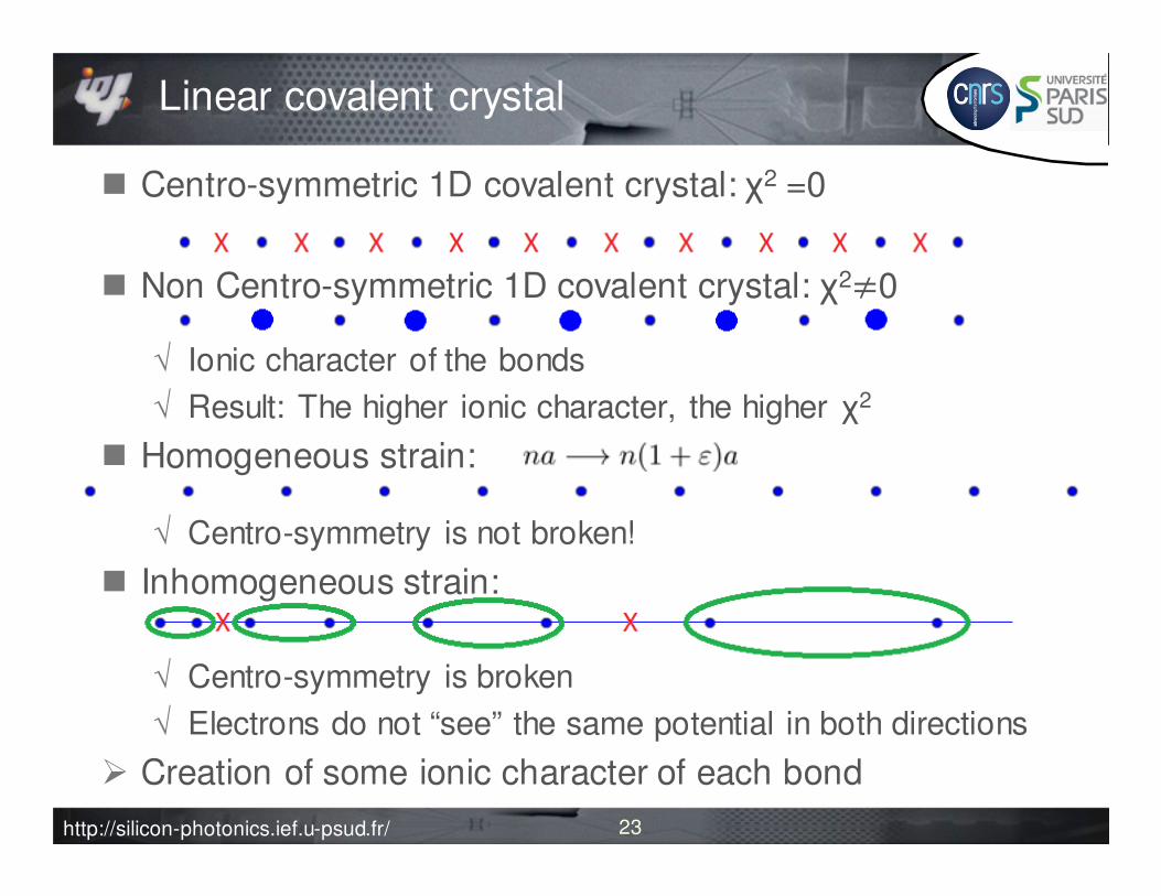
Linear covalent crystal
23
� Centro-symmetric 1D covalent crystal: χ2 =0
� Non Centro-symmetric 1D covalent crystal: χ2�0
√ Ionic character of the bonds
√ Result: The higher ionic character, the higher χ2
� Homogeneous strain:
√ Centro-symmetry is not broken!
� Inhomogeneous strain:
√ Centro-symmetry is broken
√ Electrons do not “see” the same potential in both directions
� Creation of some ionic character of each bond

http://silicon-photonics.ief.u-psud.fr/
Method for comparing structures
24
Strain
� Simulations using ANSYS software
√ Calculation of strain maps
� Initial conditions:
√ Initial stress of the straining layer:
√ Obtained after fabrication conditions
�Reported in the literature
�Fabrication studies
Optical Mode
� Calculated using Mode-solver software
� Mode profile
√ Approximated by a 2D gaussiansurface
� Gaussian parameters imported to ANSYS
√ Overlaps are performed
� Structures Comparison
√ Looped in ANSYS
√ Extraction of the effective value

http://silicon-photonics.ief.u-psud.fr/
Simulations
� Nonlinear effects:
√ Overlap between optical mode and χ2 distributions
√ Overlap between optical mode and strain gradient distributions
Optical mode YY Strain Map
25

http://silicon-photonics.ief.u-psud.fr/
Strain gradients
� StrainYY map:
26

http://silicon-photonics.ief.u-psud.fr/
Optical mode and overlap
� Optical mode
27

http://silicon-photonics.ief.u-psud.fr/
Final effective value
� … now we integrate over all the path
Final effective number:
Sum of the contributions of every path:
The final will be used to
compare different structures
28
Final effective value of the considered path

http://silicon-photonics.ief.u-psud.fr/
Symmetry considerations
� In a symmetric structure
√ Strain and profiles are symmetric in x direction
√ Strain gradient profile is antisymmetric in x direction
�Symmetric but opposite signs
√ The gradients in X direction do not contribute to χ2
� In X symmetric waveguides, only the Y direction
gradients contribute to χ2
29
Thus

http://silicon-photonics.ief.u-psud.fr/
-60
-55
-50
-45
-40
-35
-30
1520 1530 1540 1550 1560 1570
T (
db
)
λ (nm)
First experimental tests: Mzi modulator
� Technique PECVD
√ Expected 1GPa stress
� Assymetric MZI
√ Different arm lengths
� Transmission Spectra
� Very clear transmission
spectra from the MZI
30
-60
-55
-50
-45
-40
-35
-30
1525 1530 1535 1540
T (
db
)λ (nm)
0V
25V

http://silicon-photonics.ief.u-psud.fr/
Conclusion:
Most important results so far…
� Χ2 depends on the
gradients of strain
√ Every component of
strain
√ Gradients in every
direction
� Homogeneous strain
√ Does not contribute to χ2
generation
� Waveguide symmetries
in one direction
√ No contribution of
strain gradients in that direction
√ Symmetric waveguides have less contributions
to χ2 generation
31
� Look for structures with…
√ Higher Gradients of strain
√ Higher structural asymmetries

http://silicon-photonics.ief.u-psud.fr/ 32
Acknowledgements:
Funding and collaborations
National Research Agency
SILVER, MICROS, GOSPEL, MASSTOR, ULTIMATE, Ca-Re-Lase, POSISLOT
Plat4M
photonic libraries and technology for manufacturing
SASER
Safe and Secure European Routing
HELIOS
Photonics Electronics functional integration on CMOS
Silicon photonics group