Embed Size (px)
Citation preview
Microstrip-Slot Transition and Its Applications in Multilayer Microwave Circuits 247
Microstrip-Slot Transition and Its Applications in Multilayer Microwave Circuits
Norhudah Seman and Marek E. Bialkowski
x
Microstrip-Slot Transition and Its Applications in Multilayer Microwave Circuits
Norhudah Seman1,2 and Marek E. Bialkowski1
1The University of Queensland Australia
2Universiti Teknologi Malaysia Malaysia
1. Introduction
The rapid development of wireless communication systems has put a lot of demand for compact RF fronts. Nowadays, these subsystems mostly operate in microwave frequency bands and include amplifiers, filters and mixers, which are accompanied by lumped capacitors, inductors, resistors and distributed circuits in the form of sections of transmission lines. With regard to the choice of technology, planar technology including microstrip, stripline, slotline or coplanar waveguide is preferred for an RF front end design because of low manufacturing cost. The demand on minimizing the occupied area by RF front end requires utilization of two sides of substrates on which passive and active devices are to be developed. A further demand on compactness calls for use of a multilayer planar approach. In such cases, the challenge is in passing a signal between two sides of a dielectric layer. A suitable transition (also named via) of wire or wireless type is required to accomplish this task. To couple DC signals wire-type transitions are unavoidable. However, when only a RF signal has to be passed, a wireless via can be a more convenient choice. The most common transition for coupling a RF signal between two sides of planar dielectric structure is the microstrip-to-slotline transition. Its convenience is that it achieves this function using wireless means, making the manufacturing process cost effective. It is important to understand the fundamental properties of this transition, as well as it is imperative to have its design guidelines. Also it is important to know its applications in basic microwave circuits and devices. This chapter provides an overview of design of a microstrip-slot transition, explains its operation and gives examples in which such transition can play a useful role.
2. Microstrip-Slot Transition
A microstrip-slot transition is a structure that uses a microstrip line on one side of a planar dielectric substrate and a slotline in the ground so that a signal is passed between the two sides. In order to perform this function with minimal power losses, the microstrip line and
12
www.intechopen.com
Passive Microwave Components and Antennas248
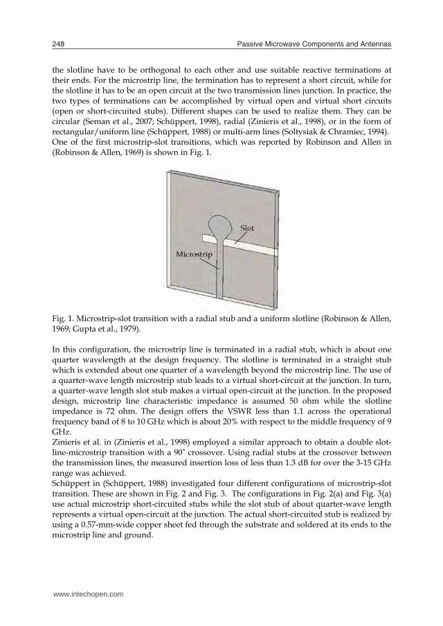
the slotline have to be orthogonal to each other and use suitable reactive terminations at their ends. For the microstrip line, the termination has to represent a short circuit, while for the slotline it has to be an open circuit at the two transmission lines junction. In practice, the two types of terminations can be accomplished by virtual open and virtual short circuits (open or short-circuited stubs). Different shapes can be used to realize them. They can be circular (Seman et al., 2007; Schüppert, 1998), radial (Zinieris et al., 1998), or in the form of rectangular/uniform line (Schüppert, 1988) or multi-arm lines (Soltysiak & Chramiec, 1994). One of the first microstrip-slot transitions, which was reported by Robinson and Allen in (Robinson & Allen, 1969) is shown in Fig. 1.
Fig. 1. Microstrip-slot transition with a radial stub and a uniform slotline (Robinson & Allen, 1969; Gupta et al., 1979). In this configuration, the microstrip line is terminated in a radial stub, which is about one quarter wavelength at the design frequency. The slotline is terminated in a straight stub which is extended about one quarter of a wavelength beyond the microstrip line. The use of a quarter-wave length microstrip stub leads to a virtual short-circuit at the junction. In turn, a quarter-wave length slot stub makes a virtual open-circuit at the junction. In the proposed design, microstrip line characteristic impedance is assumed 50 ohm while the slotline impedance is 72 ohm. The design offers the VSWR less than 1.1 across the operational frequency band of 8 to 10 GHz which is about 20% with respect to the middle frequency of 9 GHz. Zinieris et al. in (Zinieris et al., 1998) employed a similar approach to obtain a double slot-line-microstrip transition with a 90 crossover. Using radial stubs at the crossover between the transmission lines, the measured insertion loss of less than 1.3 dB for over the 3-15 GHz range was achieved. Schüppert in (Schüppert, 1988) investigated four different configurations of microstrip-slot transition. These are shown in Fig. 2 and Fig. 3. The configurations in Fig. 2(a) and Fig. 3(a) use actual microstrip short-circuited stubs while the slot stub of about quarter-wave length represents a virtual open-circuit at the junction. The actual short-circuited stub is realized by using a 0.57-mm-wide copper sheet fed through the substrate and soldered at its ends to the microstrip line and ground.
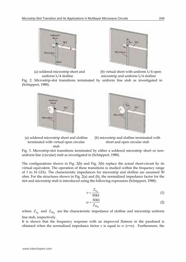
(a) soldered microstrip short and (b) virtual short with uniform λ/4 open uniform λ/4 slotline microstrip and uniform λ/4 slotline Fig. 2. Microstrip-slot transitions terminated by uniform line stub as investigated in (Schüppert, 1988).
(a) soldered microstrip short and slotline
terminated with virtual open circular stub
(b) microstrip and slotline terminated with
short and open circular stub
Fig. 3. Microstrip-slot transitions terminated by either a soldered microstrip short or non-uniform line (circular) stub as investigated in (Schüppert, 1988). The configurations shown in Fig. 2(b) and Fig. 3(b) replace the actual short-circuit by its virtual equivalent. The operation of these transitions is studied within the frequency range of 1 to 16 GHz. The characteristic impedances for microstrip and slotline are assumed 50 ohm. For the structures shown in Fig. 2(a) and (b), the normalized impedance factor for the slot and microstrip stub is introduced using the following expression (Schüppert, 1988):
50
ssZv (1)
smZ
w 50 (2)
where ssZ and smZ are the characteristic impedance of slotline and microstrip uniform
line stub, respectively. It is shown that the frequency response with an improved flatness in the passband is obtained when the normalized impedance factor v is equal to w (v=w). Furthermore, the
www.intechopen.com
Microstrip-Slot Transition and Its Applications in Multilayer Microwave Circuits 249
the slotline have to be orthogonal to each other and use suitable reactive terminations at their ends. For the microstrip line, the termination has to represent a short circuit, while for the slotline it has to be an open circuit at the two transmission lines junction. In practice, the two types of terminations can be accomplished by virtual open and virtual short circuits (open or short-circuited stubs). Different shapes can be used to realize them. They can be circular (Seman et al., 2007; Schüppert, 1998), radial (Zinieris et al., 1998), or in the form of rectangular/uniform line (Schüppert, 1988) or multi-arm lines (Soltysiak & Chramiec, 1994). One of the first microstrip-slot transitions, which was reported by Robinson and Allen in (Robinson & Allen, 1969) is shown in Fig. 1.
Fig. 1. Microstrip-slot transition with a radial stub and a uniform slotline (Robinson & Allen, 1969; Gupta et al., 1979). In this configuration, the microstrip line is terminated in a radial stub, which is about one quarter wavelength at the design frequency. The slotline is terminated in a straight stub which is extended about one quarter of a wavelength beyond the microstrip line. The use of a quarter-wave length microstrip stub leads to a virtual short-circuit at the junction. In turn, a quarter-wave length slot stub makes a virtual open-circuit at the junction. In the proposed design, microstrip line characteristic impedance is assumed 50 ohm while the slotline impedance is 72 ohm. The design offers the VSWR less than 1.1 across the operational frequency band of 8 to 10 GHz which is about 20% with respect to the middle frequency of 9 GHz. Zinieris et al. in (Zinieris et al., 1998) employed a similar approach to obtain a double slot-line-microstrip transition with a 90 crossover. Using radial stubs at the crossover between the transmission lines, the measured insertion loss of less than 1.3 dB for over the 3-15 GHz range was achieved. Schüppert in (Schüppert, 1988) investigated four different configurations of microstrip-slot transition. These are shown in Fig. 2 and Fig. 3. The configurations in Fig. 2(a) and Fig. 3(a) use actual microstrip short-circuited stubs while the slot stub of about quarter-wave length represents a virtual open-circuit at the junction. The actual short-circuited stub is realized by using a 0.57-mm-wide copper sheet fed through the substrate and soldered at its ends to the microstrip line and ground.
(a) soldered microstrip short and (b) virtual short with uniform λ/4 open uniform λ/4 slotline microstrip and uniform λ/4 slotline Fig. 2. Microstrip-slot transitions terminated by uniform line stub as investigated in (Schüppert, 1988).
(a) soldered microstrip short and slotline
terminated with virtual open circular stub
(b) microstrip and slotline terminated with
short and open circular stub
Fig. 3. Microstrip-slot transitions terminated by either a soldered microstrip short or non-uniform line (circular) stub as investigated in (Schüppert, 1988). The configurations shown in Fig. 2(b) and Fig. 3(b) replace the actual short-circuit by its virtual equivalent. The operation of these transitions is studied within the frequency range of 1 to 16 GHz. The characteristic impedances for microstrip and slotline are assumed 50 ohm. For the structures shown in Fig. 2(a) and (b), the normalized impedance factor for the slot and microstrip stub is introduced using the following expression (Schüppert, 1988):
50
ssZv (1)
smZ
w 50 (2)
where ssZ and smZ are the characteristic impedance of slotline and microstrip uniform
line stub, respectively. It is shown that the frequency response with an improved flatness in the passband is obtained when the normalized impedance factor v is equal to w (v=w). Furthermore, the
www.intechopen.com
Passive Microwave Components and Antennas250
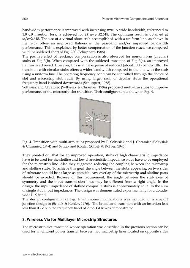
bandwidth performance is improved with increasing v=w. A wide bandwidth, referenced to 1.0 dB insertion loss, is achieved for 2≤ w/v ≤2.618. The optimum result is obtained at w/v=2.618. The use of a virtual short stub accomplished with a uniform line, as shown in Fig. 2(b), offers an improved flatness in the passband and/or improved bandwidth performance. This is explained by better compensation of the junction reactance compared with the soldered short of Fig. 2(a) (Schüppert, 1988). The positive effect of reactance compensation is also observed for non-uniform (circular) stubs of Fig. 3(b). When compared with the soldered transition of Fig. 3(a), an improved flatness is achieved. However, this is at the expense of reduced (about 10%) bandwidth. The transition with circular stubs offers a wider bandwidth compared to the one with the stub using a uniform line. The operating frequency band can be controlled through the choice of slot and microstrip stub radii. By using larger radii of circular stubs the operational frequency band is shifted downwards (Schüppert, 1988). Soltysiak and Chramiec (Soltysiak & Chramiec, 1994) proposed multi-arm stubs to improve performance of the microstrip-slot transition. Their configuration is shown in Fig. 4.
Fig. 4. Transition with multi-arm stubs proposed by P. Soltysiak and J. Chramiec (Soltysiak & Chramiec, 1994) and Schiek and Kohler (Schiek & Kohler, 1976). They pointed out that for an improved operation, stubs of high characteristic impedance have to be used for the slotline and low characteristic impedance stubs have to be employed for the microstrip line. Also they suggested reducing the coupling between the microstrip and slotline stubs. To achieve this goal, the angle between the stubs appearing on two sides of substrate should be as large as possible. Any overlap of the microstrip and slotline parts should be avoided. Because of this requirement, the angle between the stub axes of symmetry and the input transmission lines may be different from a right angle. In the design, the input impedance of slotline composite stubs is approximately equal to the sum of single stub input impedances. The design was demonstrated experimentally for a decade-wide L-X band. The design configuration of Fig. 4 with some modifications was included in a six-port junction design in (Schiek & Kohler, 1976). The broadband transition with an insertion loss less than 0.2 dB in the frequency band of 2 to 9 GHz was demonstrated.
3. Wireless Via for Multilayer Microstrip Structures
The microstrip-slot transition whose operation was described in the previous section can be used for an efficient power transfer between two microstrip lines located on opposite sides
of a two-dielectric layer structure that is supported by a common ground plane. Such a broadband wireless via or slice interconnect using an earlier work of Schüppert (Schüppert, 1988) was proposed in (Ho et al., 1993). This vertical interconnect is attractive because it does not use any wires to couple the signal between the two microstrip lines. Therefore it is easy to manufacture. Its importance is that it is capable to achieve a low insertion loss coupling over an ultra wide frequency band (UWB). Therefore, it can be of significance to developing compact UWB microwave multilayer front-ends. In (Ho et al., 1993), the operation of this interconnect was demonstrated using experimental means and was limited to one example. Here, its comprehensive theoretical and experimental investigation is presented. The following sections show the design of such an UWB via aimed for operation in the 3.1 to 10.6 GHz band.
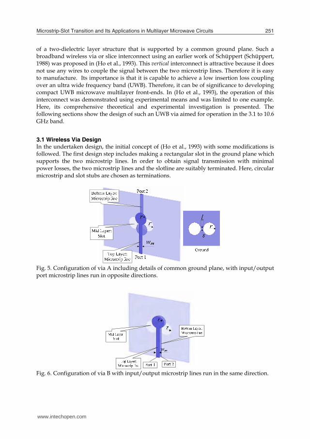
3.1 Wireless Via Design In the undertaken design, the initial concept of (Ho et al., 1993) with some modifications is followed. The first design step includes making a rectangular slot in the ground plane which supports the two microstrip lines. In order to obtain signal transmission with minimal power losses, the two microstrip lines and the slotline are suitably terminated. Here, circular microstrip and slot stubs are chosen as terminations.
Fig. 5. Configuration of via A including details of common ground plane, with input/output port microstrip lines run in opposite directions.
Fig. 6. Configuration of via B with input/output microstrip lines run in the same direction.
www.intechopen.com
Microstrip-Slot Transition and Its Applications in Multilayer Microwave Circuits 251
bandwidth performance is improved with increasing v=w. A wide bandwidth, referenced to 1.0 dB insertion loss, is achieved for 2≤ w/v ≤2.618. The optimum result is obtained at w/v=2.618. The use of a virtual short stub accomplished with a uniform line, as shown in Fig. 2(b), offers an improved flatness in the passband and/or improved bandwidth performance. This is explained by better compensation of the junction reactance compared with the soldered short of Fig. 2(a) (Schüppert, 1988). The positive effect of reactance compensation is also observed for non-uniform (circular) stubs of Fig. 3(b). When compared with the soldered transition of Fig. 3(a), an improved flatness is achieved. However, this is at the expense of reduced (about 10%) bandwidth. The transition with circular stubs offers a wider bandwidth compared to the one with the stub using a uniform line. The operating frequency band can be controlled through the choice of slot and microstrip stub radii. By using larger radii of circular stubs the operational frequency band is shifted downwards (Schüppert, 1988). Soltysiak and Chramiec (Soltysiak & Chramiec, 1994) proposed multi-arm stubs to improve performance of the microstrip-slot transition. Their configuration is shown in Fig. 4.
Fig. 4. Transition with multi-arm stubs proposed by P. Soltysiak and J. Chramiec (Soltysiak & Chramiec, 1994) and Schiek and Kohler (Schiek & Kohler, 1976). They pointed out that for an improved operation, stubs of high characteristic impedance have to be used for the slotline and low characteristic impedance stubs have to be employed for the microstrip line. Also they suggested reducing the coupling between the microstrip and slotline stubs. To achieve this goal, the angle between the stubs appearing on two sides of substrate should be as large as possible. Any overlap of the microstrip and slotline parts should be avoided. Because of this requirement, the angle between the stub axes of symmetry and the input transmission lines may be different from a right angle. In the design, the input impedance of slotline composite stubs is approximately equal to the sum of single stub input impedances. The design was demonstrated experimentally for a decade-wide L-X band. The design configuration of Fig. 4 with some modifications was included in a six-port junction design in (Schiek & Kohler, 1976). The broadband transition with an insertion loss less than 0.2 dB in the frequency band of 2 to 9 GHz was demonstrated.
3. Wireless Via for Multilayer Microstrip Structures
The microstrip-slot transition whose operation was described in the previous section can be used for an efficient power transfer between two microstrip lines located on opposite sides
of a two-dielectric layer structure that is supported by a common ground plane. Such a broadband wireless via or slice interconnect using an earlier work of Schüppert (Schüppert, 1988) was proposed in (Ho et al., 1993). This vertical interconnect is attractive because it does not use any wires to couple the signal between the two microstrip lines. Therefore it is easy to manufacture. Its importance is that it is capable to achieve a low insertion loss coupling over an ultra wide frequency band (UWB). Therefore, it can be of significance to developing compact UWB microwave multilayer front-ends. In (Ho et al., 1993), the operation of this interconnect was demonstrated using experimental means and was limited to one example. Here, its comprehensive theoretical and experimental investigation is presented. The following sections show the design of such an UWB via aimed for operation in the 3.1 to 10.6 GHz band.
3.1 Wireless Via Design In the undertaken design, the initial concept of (Ho et al., 1993) with some modifications is followed. The first design step includes making a rectangular slot in the ground plane which supports the two microstrip lines. In order to obtain signal transmission with minimal power losses, the two microstrip lines and the slotline are suitably terminated. Here, circular microstrip and slot stubs are chosen as terminations.
Fig. 5. Configuration of via A including details of common ground plane, with input/output port microstrip lines run in opposite directions.
Fig. 6. Configuration of via B with input/output microstrip lines run in the same direction.
www.intechopen.com
Passive Microwave Components and Antennas252
The role of virtual open circular stubs at the ends of slotline is to enforce the maximum electromagnetic power flow through the coupling slot (Ho et al., 1993). Following the recommendations in (Schüppert, 1988) and (Ho et al., 1993), the slot width is chosen such that the 50 ohm impedance is observed from the microstrip side. A better performance is expected for smaller values of impedance. However, they face manufacturing limitations because smaller characteristic impedances of slotline require a very narrow slot. Here, investigations include two types of this interconnect, which are named here as via A and B. They are shown in Fig. 5 and Fig. 6. The difference between these two configurations is the direction of the output microstrip transmission lines. Via A has its output microstrip lines in the opposite directions while via B uses them in the same direction. Assuming that the microstrip lines have a characteristic impedance of 50 ohm, the aim is to choose suitable dimensions of a virtual microstrip short circuit and a virtual slotline open circuit so that a broadband performance in terms of low insertion losses and high return losses is obtained. The design is assisted with the full EM-wave simulation package, CST Microwave Studio (CST MWS). The design assumes a double layer of Rogers RO4003 substrate with dielectric constant of 3.38 and thickness of 0.508 mm.
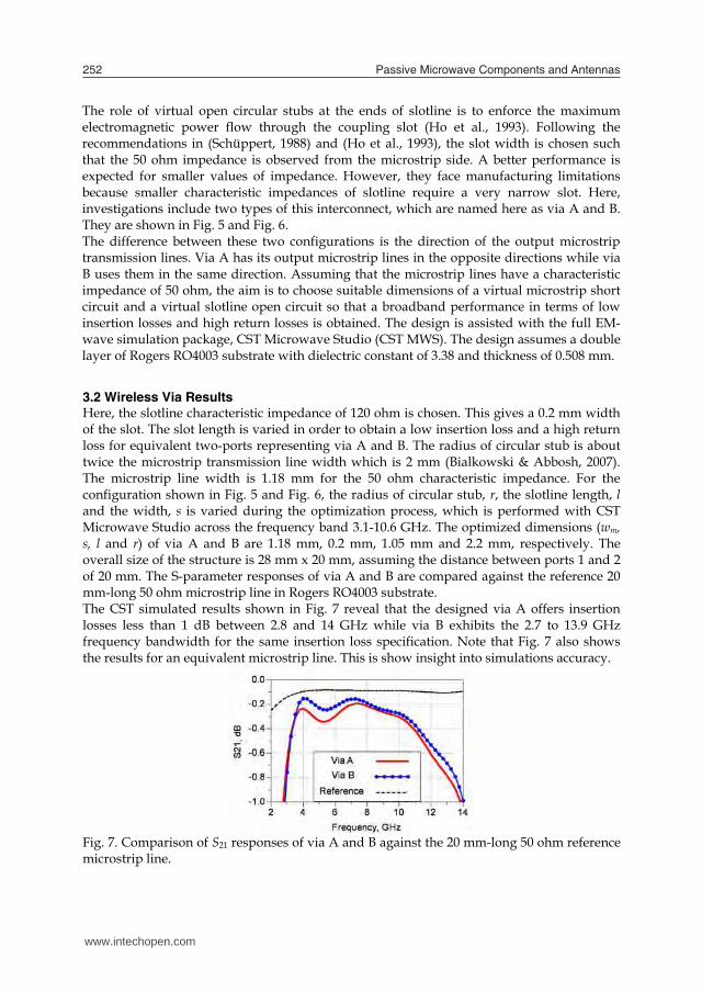
3.2 Wireless Via Results Here, the slotline characteristic impedance of 120 ohm is chosen. This gives a 0.2 mm width of the slot. The slot length is varied in order to obtain a low insertion loss and a high return loss for equivalent two-ports representing via A and B. The radius of circular stub is about twice the microstrip transmission line width which is 2 mm (Bialkowski & Abbosh, 2007). The microstrip line width is 1.18 mm for the 50 ohm characteristic impedance. For the configuration shown in Fig. 5 and Fig. 6, the radius of circular stub, r, the slotline length, l and the width, s is varied during the optimization process, which is performed with CST Microwave Studio across the frequency band 3.1-10.6 GHz. The optimized dimensions (wm, s, l and r) of via A and B are 1.18 mm, 0.2 mm, 1.05 mm and 2.2 mm, respectively. The overall size of the structure is 28 mm x 20 mm, assuming the distance between ports 1 and 2 of 20 mm. The S-parameter responses of via A and B are compared against the reference 20 mm-long 50 ohm microstrip line in Rogers RO4003 substrate. The CST simulated results shown in Fig. 7 reveal that the designed via A offers insertion losses less than 1 dB between 2.8 and 14 GHz while via B exhibits the 2.7 to 13.9 GHz frequency bandwidth for the same insertion loss specification. Note that Fig. 7 also shows the results for an equivalent microstrip line. This is show insight into simulations accuracy.
Fig. 7. Comparison of S21 responses of via A and B against the 20 mm-long 50 ohm reference microstrip line.
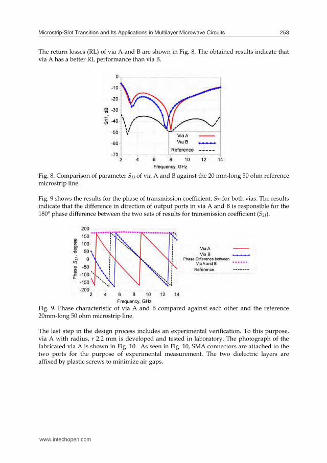
The return losses (RL) of via A and B are shown in Fig. 8. The obtained results indicate that via A has a better RL performance than via B.
Fig. 8. Comparison of parameter S11 of via A and B against the 20 mm-long 50 ohm reference microstrip line. Fig. 9 shows the results for the phase of transmission coefficient, S21 for both vias. The results indicate that the difference in direction of output ports in via A and B is responsible for the 180° phase difference between the two sets of results for transmission coefficient (S21).
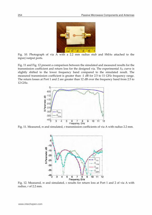
Fig. 9. Phase characteristic of via A and B compared against each other and the reference 20mm-long 50 ohm microstrip line. The last step in the design process includes an experimental verification. To this purpose, via A with radius, r 2.2 mm is developed and tested in laboratory. The photograph of the fabricated via A is shown in Fig. 10. As seen in Fig. 10, SMA connectors are attached to the two ports for the purpose of experimental measurement. The two dielectric layers are affixed by plastic screws to minimize air gaps.
www.intechopen.com
Microstrip-Slot Transition and Its Applications in Multilayer Microwave Circuits 253
The role of virtual open circular stubs at the ends of slotline is to enforce the maximum electromagnetic power flow through the coupling slot (Ho et al., 1993). Following the recommendations in (Schüppert, 1988) and (Ho et al., 1993), the slot width is chosen such that the 50 ohm impedance is observed from the microstrip side. A better performance is expected for smaller values of impedance. However, they face manufacturing limitations because smaller characteristic impedances of slotline require a very narrow slot. Here, investigations include two types of this interconnect, which are named here as via A and B. They are shown in Fig. 5 and Fig. 6. The difference between these two configurations is the direction of the output microstrip transmission lines. Via A has its output microstrip lines in the opposite directions while via B uses them in the same direction. Assuming that the microstrip lines have a characteristic impedance of 50 ohm, the aim is to choose suitable dimensions of a virtual microstrip short circuit and a virtual slotline open circuit so that a broadband performance in terms of low insertion losses and high return losses is obtained. The design is assisted with the full EM-wave simulation package, CST Microwave Studio (CST MWS). The design assumes a double layer of Rogers RO4003 substrate with dielectric constant of 3.38 and thickness of 0.508 mm.
3.2 Wireless Via Results Here, the slotline characteristic impedance of 120 ohm is chosen. This gives a 0.2 mm width of the slot. The slot length is varied in order to obtain a low insertion loss and a high return loss for equivalent two-ports representing via A and B. The radius of circular stub is about twice the microstrip transmission line width which is 2 mm (Bialkowski & Abbosh, 2007). The microstrip line width is 1.18 mm for the 50 ohm characteristic impedance. For the configuration shown in Fig. 5 and Fig. 6, the radius of circular stub, r, the slotline length, l and the width, s is varied during the optimization process, which is performed with CST Microwave Studio across the frequency band 3.1-10.6 GHz. The optimized dimensions (wm, s, l and r) of via A and B are 1.18 mm, 0.2 mm, 1.05 mm and 2.2 mm, respectively. The overall size of the structure is 28 mm x 20 mm, assuming the distance between ports 1 and 2 of 20 mm. The S-parameter responses of via A and B are compared against the reference 20 mm-long 50 ohm microstrip line in Rogers RO4003 substrate. The CST simulated results shown in Fig. 7 reveal that the designed via A offers insertion losses less than 1 dB between 2.8 and 14 GHz while via B exhibits the 2.7 to 13.9 GHz frequency bandwidth for the same insertion loss specification. Note that Fig. 7 also shows the results for an equivalent microstrip line. This is show insight into simulations accuracy.
Fig. 7. Comparison of S21 responses of via A and B against the 20 mm-long 50 ohm reference microstrip line.
The return losses (RL) of via A and B are shown in Fig. 8. The obtained results indicate that via A has a better RL performance than via B.
Fig. 8. Comparison of parameter S11 of via A and B against the 20 mm-long 50 ohm reference microstrip line. Fig. 9 shows the results for the phase of transmission coefficient, S21 for both vias. The results indicate that the difference in direction of output ports in via A and B is responsible for the 180° phase difference between the two sets of results for transmission coefficient (S21).
Fig. 9. Phase characteristic of via A and B compared against each other and the reference 20mm-long 50 ohm microstrip line. The last step in the design process includes an experimental verification. To this purpose, via A with radius, r 2.2 mm is developed and tested in laboratory. The photograph of the fabricated via A is shown in Fig. 10. As seen in Fig. 10, SMA connectors are attached to the two ports for the purpose of experimental measurement. The two dielectric layers are affixed by plastic screws to minimize air gaps.
www.intechopen.com
Passive Microwave Components and Antennas254
Fig. 10. Photograph of via A with a 2.2 mm radius stub and SMAs attached to the input/output ports. Fig. 11 and Fig. 12 present a comparison between the simulated and measured results for the transmission coefficient and return loss for the designed via. The experimental S21 curve is slightly shifted to the lower frequency band compared to the simulated result. The measured transmission coefficient is greater than -1 dB for 2.5 to 11 GHz frequency range. The return losses at Port 1 and 2 are greater than 12 dB over the frequency band from 2.5 to 12 GHz.
Fig. 11. Measured, m and simulated, s transmission coefficients of via A with radius 2.2 mm.
Fig. 12. Measured, m and simulated, s results for return loss at Port 1 and 2 of via A with radius, r of 2.2 mm.
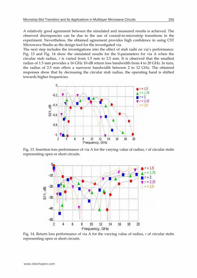
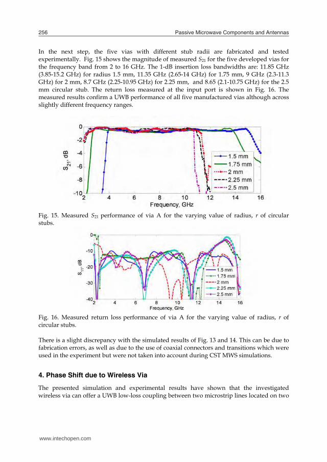
A relatively good agreement between the simulated and measured results is achieved. The observed discrepancies can be due to the use of coaxial-to-microstrip transitions in the experiment. Nevertheless, the obtained agreement provides high confidence in using CST Microwave Studio as the design tool for the investigated via. The next step includes the investigations into the effect of stub radii on via’s performance. Fig. 13 and Fig. 14 show the simulated results for the S-parameters for via A when the circular stub radius, r is varied from 1.5 mm to 2.5 mm. It is observed that the smallest radius of 1.5 mm provides a 16 GHz 10-dB return loss bandwidth from 4 to 20 GHz. In turn, the radius of 2.5 mm offers a narrower bandwidth between 2 to 12 GHz. The obtained responses show that by decreasing the circular stub radius, the operating band is shifted towards higher frequencies.
Fig. 13. Insertion loss performance of via A for the varying value of radius, r of circular stubs representing open or short circuits.
Fig. 14. Return loss performance of via A for the varying value of radius, r of circular stubs representing open or short circuits.
www.intechopen.com
Microstrip-Slot Transition and Its Applications in Multilayer Microwave Circuits 255
Fig. 10. Photograph of via A with a 2.2 mm radius stub and SMAs attached to the input/output ports. Fig. 11 and Fig. 12 present a comparison between the simulated and measured results for the transmission coefficient and return loss for the designed via. The experimental S21 curve is slightly shifted to the lower frequency band compared to the simulated result. The measured transmission coefficient is greater than -1 dB for 2.5 to 11 GHz frequency range. The return losses at Port 1 and 2 are greater than 12 dB over the frequency band from 2.5 to 12 GHz.
Fig. 11. Measured, m and simulated, s transmission coefficients of via A with radius 2.2 mm.
Fig. 12. Measured, m and simulated, s results for return loss at Port 1 and 2 of via A with radius, r of 2.2 mm.
A relatively good agreement between the simulated and measured results is achieved. The observed discrepancies can be due to the use of coaxial-to-microstrip transitions in the experiment. Nevertheless, the obtained agreement provides high confidence in using CST Microwave Studio as the design tool for the investigated via. The next step includes the investigations into the effect of stub radii on via’s performance. Fig. 13 and Fig. 14 show the simulated results for the S-parameters for via A when the circular stub radius, r is varied from 1.5 mm to 2.5 mm. It is observed that the smallest radius of 1.5 mm provides a 16 GHz 10-dB return loss bandwidth from 4 to 20 GHz. In turn, the radius of 2.5 mm offers a narrower bandwidth between 2 to 12 GHz. The obtained responses show that by decreasing the circular stub radius, the operating band is shifted towards higher frequencies.
Fig. 13. Insertion loss performance of via A for the varying value of radius, r of circular stubs representing open or short circuits.
Fig. 14. Return loss performance of via A for the varying value of radius, r of circular stubs representing open or short circuits.
www.intechopen.com
Passive Microwave Components and Antennas256
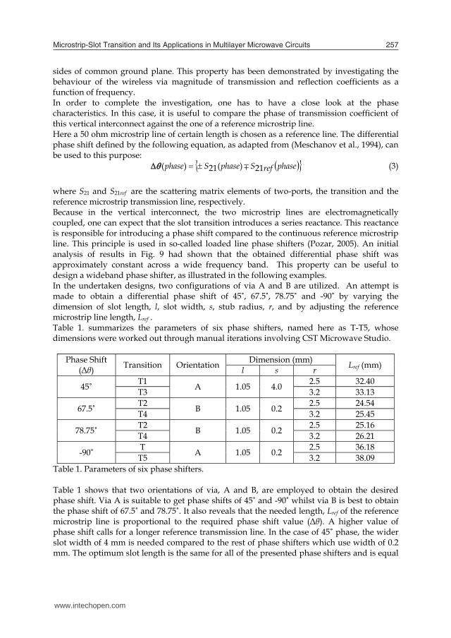
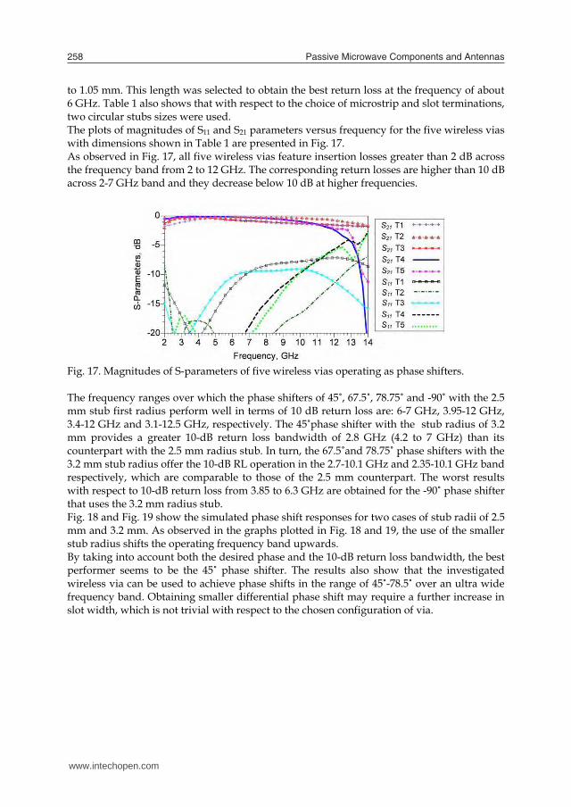
In the next step, the five vias with different stub radii are fabricated and tested experimentally. Fig. 15 shows the magnitude of measured S21 for the five developed vias for the frequency band from 2 to 16 GHz. The 1-dB insertion loss bandwidths are: 11.85 GHz (3.85-15.2 GHz) for radius 1.5 mm, 11.35 GHz (2.65-14 GHz) for 1.75 mm, 9 GHz (2.3-11.3 GHz) for 2 mm, 8.7 GHz (2.25-10.95 GHz) for 2.25 mm, and 8.65 (2.1-10.75 GHz) for the 2.5 mm circular stub. The return loss measured at the input port is shown in Fig. 16. The measured results confirm a UWB performance of all five manufactured vias although across slightly different frequency ranges.
Fig. 15. Measured S21 performance of via A for the varying value of radius, r of circular stubs.
Fig. 16. Measured return loss performance of via A for the varying value of radius, r of circular stubs. There is a slight discrepancy with the simulated results of Fig. 13 and 14. This can be due to fabrication errors, as well as due to the use of coaxial connectors and transitions which were used in the experiment but were not taken into account during CST MWS simulations.
4. Phase Shift due to Wireless Via
The presented simulation and experimental results have shown that the investigated wireless via can offer a UWB low-loss coupling between two microstrip lines located on two
sides of common ground plane. This property has been demonstrated by investigating the behaviour of the wireless via magnitude of transmission and reflection coefficients as a function of frequency. In order to complete the investigation, one has to have a close look at the phase characteristics. In this case, it is useful to compare the phase of transmission coefficient of this vertical interconnect against the one of a reference microstrip line. Here a 50 ohm microstrip line of certain length is chosen as a reference line. The differential phase shift defined by the following equation, as adapted from (Meschanov et al., 1994), can be used to this purpose: phaserefSphaseSphase 21)(21)( (3)
where S21 and S21ref are the scattering matrix elements of two-ports, the transition and the reference microstrip transmission line, respectively. Because in the vertical interconnect, the two microstrip lines are electromagnetically coupled, one can expect that the slot transition introduces a series reactance. This reactance is responsible for introducing a phase shift compared to the continuous reference microstrip line. This principle is used in so-called loaded line phase shifters (Pozar, 2005). An initial analysis of results in Fig. 9 had shown that the obtained differential phase shift was approximately constant across a wide frequency band. This property can be useful to design a wideband phase shifter, as illustrated in the following examples. In the undertaken designs, two configurations of via A and B are utilized. An attempt is made to obtain a differential phase shift of 45, 67.5, 78.75 and -90 by varying the dimension of slot length, l, slot width, s, stub radius, r, and by adjusting the reference microstrip line length, Lref . Table 1. summarizes the parameters of six phase shifters, named here as T-T5, whose dimensions were worked out through manual iterations involving CST Microwave Studio.
Phase Shift (Δθ) Transition Orientation Dimension (mm) Lref (mm) l s r
45 T1 A 1.05 4.0 2.5 32.40 T3 3.2 33.13
67.5 T2 B 1.05 0.2 2.5 24.54 T4 3.2 25.45
78.75 T2 B 1.05 0.2 2.5 25.16 T4 3.2 26.21
-90 T A 1.05 0.2 2.5 36.18 T5 3.2 38.09
Table 1. Parameters of six phase shifters. Table 1 shows that two orientations of via, A and B, are employed to obtain the desired phase shift. Via A is suitable to get phase shifts of 45 and -90 whilst via B is best to obtain the phase shift of 67.5 and 78.75. It also reveals that the needed length, Lref of the reference microstrip line is proportional to the required phase shift value (Δθ). A higher value of phase shift calls for a longer reference transmission line. In the case of 45 phase, the wider slot width of 4 mm is needed compared to the rest of phase shifters which use width of 0.2 mm. The optimum slot length is the same for all of the presented phase shifters and is equal
www.intechopen.com
Microstrip-Slot Transition and Its Applications in Multilayer Microwave Circuits 257
In the next step, the five vias with different stub radii are fabricated and tested experimentally. Fig. 15 shows the magnitude of measured S21 for the five developed vias for the frequency band from 2 to 16 GHz. The 1-dB insertion loss bandwidths are: 11.85 GHz (3.85-15.2 GHz) for radius 1.5 mm, 11.35 GHz (2.65-14 GHz) for 1.75 mm, 9 GHz (2.3-11.3 GHz) for 2 mm, 8.7 GHz (2.25-10.95 GHz) for 2.25 mm, and 8.65 (2.1-10.75 GHz) for the 2.5 mm circular stub. The return loss measured at the input port is shown in Fig. 16. The measured results confirm a UWB performance of all five manufactured vias although across slightly different frequency ranges.
Fig. 15. Measured S21 performance of via A for the varying value of radius, r of circular stubs.
Fig. 16. Measured return loss performance of via A for the varying value of radius, r of circular stubs. There is a slight discrepancy with the simulated results of Fig. 13 and 14. This can be due to fabrication errors, as well as due to the use of coaxial connectors and transitions which were used in the experiment but were not taken into account during CST MWS simulations.
4. Phase Shift due to Wireless Via
The presented simulation and experimental results have shown that the investigated wireless via can offer a UWB low-loss coupling between two microstrip lines located on two
sides of common ground plane. This property has been demonstrated by investigating the behaviour of the wireless via magnitude of transmission and reflection coefficients as a function of frequency. In order to complete the investigation, one has to have a close look at the phase characteristics. In this case, it is useful to compare the phase of transmission coefficient of this vertical interconnect against the one of a reference microstrip line. Here a 50 ohm microstrip line of certain length is chosen as a reference line. The differential phase shift defined by the following equation, as adapted from (Meschanov et al., 1994), can be used to this purpose: phaserefSphaseSphase 21)(21)( (3)
where S21 and S21ref are the scattering matrix elements of two-ports, the transition and the reference microstrip transmission line, respectively. Because in the vertical interconnect, the two microstrip lines are electromagnetically coupled, one can expect that the slot transition introduces a series reactance. This reactance is responsible for introducing a phase shift compared to the continuous reference microstrip line. This principle is used in so-called loaded line phase shifters (Pozar, 2005). An initial analysis of results in Fig. 9 had shown that the obtained differential phase shift was approximately constant across a wide frequency band. This property can be useful to design a wideband phase shifter, as illustrated in the following examples. In the undertaken designs, two configurations of via A and B are utilized. An attempt is made to obtain a differential phase shift of 45, 67.5, 78.75 and -90 by varying the dimension of slot length, l, slot width, s, stub radius, r, and by adjusting the reference microstrip line length, Lref . Table 1. summarizes the parameters of six phase shifters, named here as T-T5, whose dimensions were worked out through manual iterations involving CST Microwave Studio.
Phase Shift (Δθ) Transition Orientation Dimension (mm) Lref (mm) l s r
45 T1 A 1.05 4.0 2.5 32.40 T3 3.2 33.13
67.5 T2 B 1.05 0.2 2.5 24.54 T4 3.2 25.45
78.75 T2 B 1.05 0.2 2.5 25.16 T4 3.2 26.21
-90 T A 1.05 0.2 2.5 36.18 T5 3.2 38.09
Table 1. Parameters of six phase shifters. Table 1 shows that two orientations of via, A and B, are employed to obtain the desired phase shift. Via A is suitable to get phase shifts of 45 and -90 whilst via B is best to obtain the phase shift of 67.5 and 78.75. It also reveals that the needed length, Lref of the reference microstrip line is proportional to the required phase shift value (Δθ). A higher value of phase shift calls for a longer reference transmission line. In the case of 45 phase, the wider slot width of 4 mm is needed compared to the rest of phase shifters which use width of 0.2 mm. The optimum slot length is the same for all of the presented phase shifters and is equal
www.intechopen.com
Passive Microwave Components and Antennas258
to 1.05 mm. This length was selected to obtain the best return loss at the frequency of about 6 GHz. Table 1 also shows that with respect to the choice of microstrip and slot terminations, two circular stubs sizes were used. The plots of magnitudes of S11 and S21 parameters versus frequency for the five wireless vias with dimensions shown in Table 1 are presented in Fig. 17. As observed in Fig. 17, all five wireless vias feature insertion losses greater than 2 dB across the frequency band from 2 to 12 GHz. The corresponding return losses are higher than 10 dB across 2-7 GHz band and they decrease below 10 dB at higher frequencies.
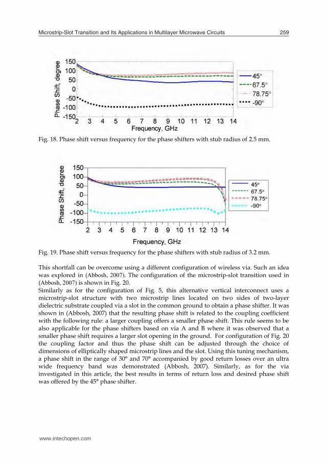
Fig. 17. Magnitudes of S-parameters of five wireless vias operating as phase shifters. The frequency ranges over which the phase shifters of 45, 67.5, 78.75 and -90 with the 2.5 mm stub first radius perform well in terms of 10 dB return loss are: 6-7 GHz, 3.95-12 GHz, 3.4-12 GHz and 3.1-12.5 GHz, respectively. The 45phase shifter with the stub radius of 3.2 mm provides a greater 10-dB return loss bandwidth of 2.8 GHz (4.2 to 7 GHz) than its counterpart with the 2.5 mm radius stub. In turn, the 67.5and 78.75 phase shifters with the 3.2 mm stub radius offer the 10-dB RL operation in the 2.7-10.1 GHz and 2.35-10.1 GHz band respectively, which are comparable to those of the 2.5 mm counterpart. The worst results with respect to 10-dB return loss from 3.85 to 6.3 GHz are obtained for the -90 phase shifter that uses the 3.2 mm radius stub. Fig. 18 and Fig. 19 show the simulated phase shift responses for two cases of stub radii of 2.5 mm and 3.2 mm. As observed in the graphs plotted in Fig. 18 and 19, the use of the smaller stub radius shifts the operating frequency band upwards. By taking into account both the desired phase and the 10-dB return loss bandwidth, the best performer seems to be the 45 phase shifter. The results also show that the investigated wireless via can be used to achieve phase shifts in the range of 45-78.5 over an ultra wide frequency band. Obtaining smaller differential phase shift may require a further increase in slot width, which is not trivial with respect to the chosen configuration of via.
Fig. 18. Phase shift versus frequency for the phase shifters with stub radius of 2.5 mm.
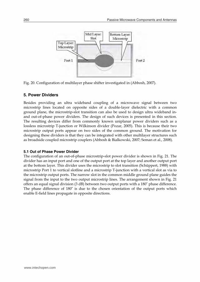
Fig. 19. Phase shift versus frequency for the phase shifters with stub radius of 3.2 mm. This shortfall can be overcome using a different configuration of wireless via. Such an idea was explored in (Abbosh, 2007). The configuration of the microstrip-slot transition used in (Abbosh, 2007) is shown in Fig. 20. Similarly as for the configuration of Fig. 5, this alternative vertical interconnect uses a microstrip-slot structure with two microstrip lines located on two sides of two-layer dielectric substrate coupled via a slot in the common ground to obtain a phase shifter. It was shown in (Abbosh, 2007) that the resulting phase shift is related to the coupling coefficient with the following rule: a larger coupling offers a smaller phase shift. This rule seems to be also applicable for the phase shifters based on via A and B where it was observed that a smaller phase shift requires a larger slot opening in the ground. For configuration of Fig. 20 the coupling factor and thus the phase shift can be adjusted through the choice of dimensions of elliptically shaped microstrip lines and the slot. Using this tuning mechanism, a phase shift in the range of 30° and 70° accompanied by good return losses over an ultra wide frequency band was demonstrated (Abbosh, 2007). Similarly, as for the via investigated in this article, the best results in terms of return loss and desired phase shift was offered by the 45° phase shifter.
www.intechopen.com
Microstrip-Slot Transition and Its Applications in Multilayer Microwave Circuits 259
to 1.05 mm. This length was selected to obtain the best return loss at the frequency of about 6 GHz. Table 1 also shows that with respect to the choice of microstrip and slot terminations, two circular stubs sizes were used. The plots of magnitudes of S11 and S21 parameters versus frequency for the five wireless vias with dimensions shown in Table 1 are presented in Fig. 17. As observed in Fig. 17, all five wireless vias feature insertion losses greater than 2 dB across the frequency band from 2 to 12 GHz. The corresponding return losses are higher than 10 dB across 2-7 GHz band and they decrease below 10 dB at higher frequencies.
Fig. 17. Magnitudes of S-parameters of five wireless vias operating as phase shifters. The frequency ranges over which the phase shifters of 45, 67.5, 78.75 and -90 with the 2.5 mm stub first radius perform well in terms of 10 dB return loss are: 6-7 GHz, 3.95-12 GHz, 3.4-12 GHz and 3.1-12.5 GHz, respectively. The 45phase shifter with the stub radius of 3.2 mm provides a greater 10-dB return loss bandwidth of 2.8 GHz (4.2 to 7 GHz) than its counterpart with the 2.5 mm radius stub. In turn, the 67.5and 78.75 phase shifters with the 3.2 mm stub radius offer the 10-dB RL operation in the 2.7-10.1 GHz and 2.35-10.1 GHz band respectively, which are comparable to those of the 2.5 mm counterpart. The worst results with respect to 10-dB return loss from 3.85 to 6.3 GHz are obtained for the -90 phase shifter that uses the 3.2 mm radius stub. Fig. 18 and Fig. 19 show the simulated phase shift responses for two cases of stub radii of 2.5 mm and 3.2 mm. As observed in the graphs plotted in Fig. 18 and 19, the use of the smaller stub radius shifts the operating frequency band upwards. By taking into account both the desired phase and the 10-dB return loss bandwidth, the best performer seems to be the 45 phase shifter. The results also show that the investigated wireless via can be used to achieve phase shifts in the range of 45-78.5 over an ultra wide frequency band. Obtaining smaller differential phase shift may require a further increase in slot width, which is not trivial with respect to the chosen configuration of via.
Fig. 18. Phase shift versus frequency for the phase shifters with stub radius of 2.5 mm.
Fig. 19. Phase shift versus frequency for the phase shifters with stub radius of 3.2 mm. This shortfall can be overcome using a different configuration of wireless via. Such an idea was explored in (Abbosh, 2007). The configuration of the microstrip-slot transition used in (Abbosh, 2007) is shown in Fig. 20. Similarly as for the configuration of Fig. 5, this alternative vertical interconnect uses a microstrip-slot structure with two microstrip lines located on two sides of two-layer dielectric substrate coupled via a slot in the common ground to obtain a phase shifter. It was shown in (Abbosh, 2007) that the resulting phase shift is related to the coupling coefficient with the following rule: a larger coupling offers a smaller phase shift. This rule seems to be also applicable for the phase shifters based on via A and B where it was observed that a smaller phase shift requires a larger slot opening in the ground. For configuration of Fig. 20 the coupling factor and thus the phase shift can be adjusted through the choice of dimensions of elliptically shaped microstrip lines and the slot. Using this tuning mechanism, a phase shift in the range of 30° and 70° accompanied by good return losses over an ultra wide frequency band was demonstrated (Abbosh, 2007). Similarly, as for the via investigated in this article, the best results in terms of return loss and desired phase shift was offered by the 45° phase shifter.
www.intechopen.com
Passive Microwave Components and Antennas260
Fig. 20. Configuration of multilayer phase shifter investigated in (Abbosh, 2007).
5. Power Dividers
Besides providing an ultra wideband coupling of a microwave signal between two microstrip lines located on opposite sides of a double-layer dielectric with a common ground plane, the microstrip-slot transition can also be used to design ultra wideband in- and out-of-phase power dividers. The design of such devices is presented in this section. The resulting devices differ from commonly known uniplanar power dividers such as a lossless microstrip T-junction or Wilkinson divider (Pozar, 2005). This is because their two microstrip output ports appear on two sides of the common ground. The motivation for designing these dividers is that they can be integrated with other multilayer structures such as broadside coupled microstrip couplers (Abbosh & Bialkowski, 2007; Seman et al., 2008).
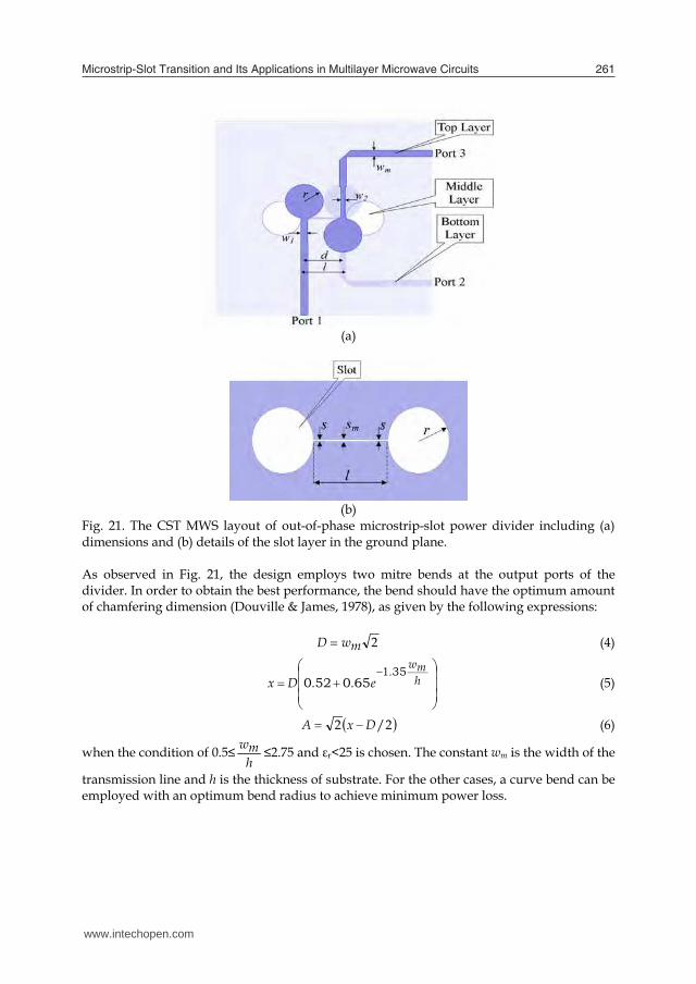
5.1 Out of Phase Power Divider The configuration of an out-of-phase microstrip-slot power divider is shown in Fig. 21. The divider has an input port and one of the output port at the top layer and another output port at the bottom layer. This divider uses the microstrip to slot transition (Schüppert, 1988) with microstrip Port 1 to vertical slotline and a microstrip T-junction with a vertical slot as via to the microstrip output ports. The narrow slot in the common middle ground plane guides the signal from the input to the two output microstrip lines. The arrangement shown in Fig. 21 offers an equal signal division (3 dB) between two output ports with a 180 phase difference. The phase difference of 180 is due to the chosen orientation of the output ports which enable E-field lines propagate in opposite directions.
(a)
(b)
Fig. 21. The CST MWS layout of out-of-phase microstrip-slot power divider including (a) dimensions and (b) details of the slot layer in the ground plane. As observed in Fig. 21, the design employs two mitre bends at the output ports of the divider. In order to obtain the best performance, the bend should have the optimum amount of chamfering dimension (Douville & James, 1978), as given by the following expressions: 2mwD (4)
hmw.
e..Dx351
650520 (5)
2/2 DxA (6)
when the condition of 0.5≤hmw ≤2.75 and εr<25 is chosen. The constant wm is the width of the
transmission line and h is the thickness of substrate. For the other cases, a curve bend can be employed with an optimum bend radius to achieve minimum power loss.
www.intechopen.com
Microstrip-Slot Transition and Its Applications in Multilayer Microwave Circuits 261
Fig. 20. Configuration of multilayer phase shifter investigated in (Abbosh, 2007).
5. Power Dividers
Besides providing an ultra wideband coupling of a microwave signal between two microstrip lines located on opposite sides of a double-layer dielectric with a common ground plane, the microstrip-slot transition can also be used to design ultra wideband in- and out-of-phase power dividers. The design of such devices is presented in this section. The resulting devices differ from commonly known uniplanar power dividers such as a lossless microstrip T-junction or Wilkinson divider (Pozar, 2005). This is because their two microstrip output ports appear on two sides of the common ground. The motivation for designing these dividers is that they can be integrated with other multilayer structures such as broadside coupled microstrip couplers (Abbosh & Bialkowski, 2007; Seman et al., 2008).
5.1 Out of Phase Power Divider The configuration of an out-of-phase microstrip-slot power divider is shown in Fig. 21. The divider has an input port and one of the output port at the top layer and another output port at the bottom layer. This divider uses the microstrip to slot transition (Schüppert, 1988) with microstrip Port 1 to vertical slotline and a microstrip T-junction with a vertical slot as via to the microstrip output ports. The narrow slot in the common middle ground plane guides the signal from the input to the two output microstrip lines. The arrangement shown in Fig. 21 offers an equal signal division (3 dB) between two output ports with a 180 phase difference. The phase difference of 180 is due to the chosen orientation of the output ports which enable E-field lines propagate in opposite directions.
(a)
(b)
Fig. 21. The CST MWS layout of out-of-phase microstrip-slot power divider including (a) dimensions and (b) details of the slot layer in the ground plane. As observed in Fig. 21, the design employs two mitre bends at the output ports of the divider. In order to obtain the best performance, the bend should have the optimum amount of chamfering dimension (Douville & James, 1978), as given by the following expressions: 2mwD (4)
hmw.
e..Dx351
650520 (5)
2/2 DxA (6)
when the condition of 0.5≤hmw ≤2.75 and εr<25 is chosen. The constant wm is the width of the
transmission line and h is the thickness of substrate. For the other cases, a curve bend can be employed with an optimum bend radius to achieve minimum power loss.
www.intechopen.com
Passive Microwave Components and Antennas262
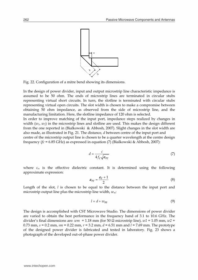
Fig. 22. Configuration of a mitre bend showing its dimensions. In the design of power divider, input and output microstrip line characteristic impedance is assumed to be 50 ohm. The ends of microstrip lines are terminated in circular stubs representing virtual short circuits. In turn, the slotline is terminated with circular stubs representing virtual open circuits. The slot width is chosen to make a compromise between obtaining 50 ohm impedance, as observed from the side of microstrip line, and the manufacturing limitation. Here, the slotline impedance of 120 ohm is selected. In order to improve matching of the input port, impedance steps realized by changes in width (w1, w2) in the microstrip lines and slotline are used. This makes the design different from the one reported in (Bialkowski & Abbosh, 2007). Slight changes in the slot width are also made, as illustrated in Fig. 21. The distance, d between centre of the input port and centre of the microstrip output line is chosen to be a quarter wavelength at the centre design frequency (fc = 6.85 GHz) as expressed in equation (7) (Bialkowski & Abbosh, 2007):
recf
cd 4 (7)
where εre is the effective dielectric constant. It is determined using the following approximate expression:
2
1 rre (8)
Length of the slot, l is chosen to be equal to the distance between the input port and microstrip output line plus the microstrip line width, wm: mwdl (9) The design is accomplished with CST Microwave Studio. The dimensions of power divider are varied to obtain the best performance in the frequency band of 3.1 to 10.6 GHz. The divider’s final dimensions are: wm = 1.18 mm (for 50 Ω microstrip line), w1 = 1.05 mm, w2 = 0.73 mm, s = 0.2 mm, sm = 0.22 mm, r = 3.2 mm, d = 6.51 mm and l = 7.69 mm. The prototype of the designed power divider is fabricated and tested in laboratory. Fig. 23 shows a photograph of the developed out-of-phase power divider.
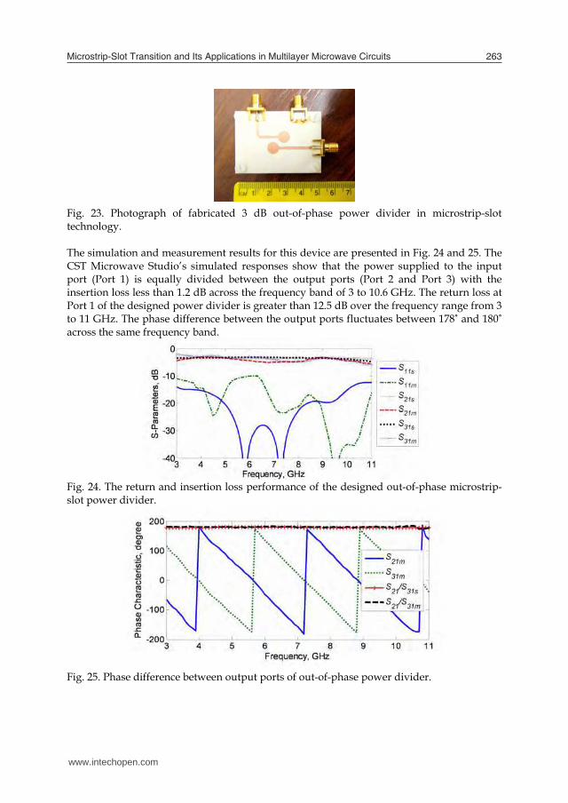
Fig. 23. Photograph of fabricated 3 dB out-of-phase power divider in microstrip-slot technology. The simulation and measurement results for this device are presented in Fig. 24 and 25. The CST Microwave Studio’s simulated responses show that the power supplied to the input port (Port 1) is equally divided between the output ports (Port 2 and Port 3) with the insertion loss less than 1.2 dB across the frequency band of 3 to 10.6 GHz. The return loss at Port 1 of the designed power divider is greater than 12.5 dB over the frequency range from 3 to 11 GHz. The phase difference between the output ports fluctuates between 178 and 180 across the same frequency band.
Fig. 24. The return and insertion loss performance of the designed out-of-phase microstrip-slot power divider.
Fig. 25. Phase difference between output ports of out-of-phase power divider.
www.intechopen.com
Microstrip-Slot Transition and Its Applications in Multilayer Microwave Circuits 263
Fig. 22. Configuration of a mitre bend showing its dimensions. In the design of power divider, input and output microstrip line characteristic impedance is assumed to be 50 ohm. The ends of microstrip lines are terminated in circular stubs representing virtual short circuits. In turn, the slotline is terminated with circular stubs representing virtual open circuits. The slot width is chosen to make a compromise between obtaining 50 ohm impedance, as observed from the side of microstrip line, and the manufacturing limitation. Here, the slotline impedance of 120 ohm is selected. In order to improve matching of the input port, impedance steps realized by changes in width (w1, w2) in the microstrip lines and slotline are used. This makes the design different from the one reported in (Bialkowski & Abbosh, 2007). Slight changes in the slot width are also made, as illustrated in Fig. 21. The distance, d between centre of the input port and centre of the microstrip output line is chosen to be a quarter wavelength at the centre design frequency (fc = 6.85 GHz) as expressed in equation (7) (Bialkowski & Abbosh, 2007):
recf
cd 4 (7)
where εre is the effective dielectric constant. It is determined using the following approximate expression:
2
1 rre (8)
Length of the slot, l is chosen to be equal to the distance between the input port and microstrip output line plus the microstrip line width, wm: mwdl (9) The design is accomplished with CST Microwave Studio. The dimensions of power divider are varied to obtain the best performance in the frequency band of 3.1 to 10.6 GHz. The divider’s final dimensions are: wm = 1.18 mm (for 50 Ω microstrip line), w1 = 1.05 mm, w2 = 0.73 mm, s = 0.2 mm, sm = 0.22 mm, r = 3.2 mm, d = 6.51 mm and l = 7.69 mm. The prototype of the designed power divider is fabricated and tested in laboratory. Fig. 23 shows a photograph of the developed out-of-phase power divider.
Fig. 23. Photograph of fabricated 3 dB out-of-phase power divider in microstrip-slot technology. The simulation and measurement results for this device are presented in Fig. 24 and 25. The CST Microwave Studio’s simulated responses show that the power supplied to the input port (Port 1) is equally divided between the output ports (Port 2 and Port 3) with the insertion loss less than 1.2 dB across the frequency band of 3 to 10.6 GHz. The return loss at Port 1 of the designed power divider is greater than 12.5 dB over the frequency range from 3 to 11 GHz. The phase difference between the output ports fluctuates between 178 and 180 across the same frequency band.
Fig. 24. The return and insertion loss performance of the designed out-of-phase microstrip-slot power divider.
Fig. 25. Phase difference between output ports of out-of-phase power divider.
www.intechopen.com
Passive Microwave Components and Antennas264
For the measured result, the average insertion losses between Port 1 and Ports 2 and 3 are 3.5 dB ± 1.43 dB from 3 to 10.4 GHz. These are slightly worse than the simulated ones. The measured return loss at Port 1 is greater than 10 dB across frequency band between 3 and 11 GHz. With respect to the phase difference between the two output ports, the fabricated prototype shows the discrepancy of ± 2 with the simulated results.
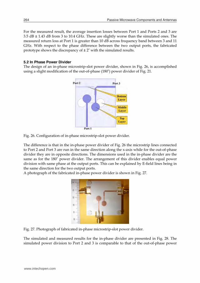
5.2 In Phase Power Divider The design of an in-phase microstrip-slot power divider, shown in Fig. 26, is accomplished using a slight modification of the out-of-phase (180) power divider of Fig. 21.
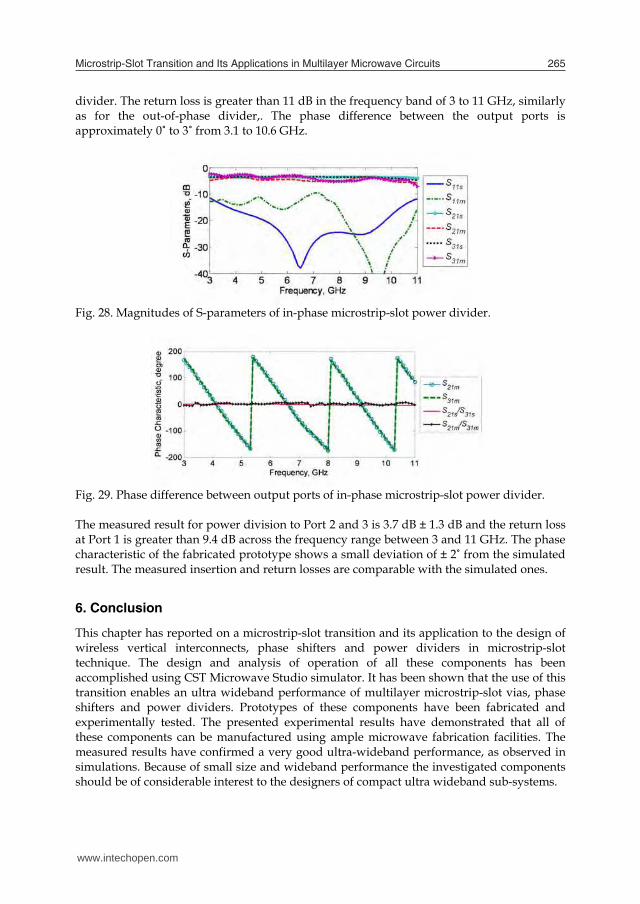
Fig. 26. Configuration of in-phase microstrip-slot power divider. The difference is that in the in-phase power divider of Fig. 26 the microstrip lines connected to Port 2 and Port 3 are run in the same direction along the x-axis while for the out-of-phase divider they are in opposite directions. The dimensions used in the in-phase divider are the same as for the 180 power divider. The arrangement of this divider enables equal power division with same phase at the output ports. This can be explained by E-field lines being in the same direction for the two output ports. A photograph of the fabricated in-phase power divider is shown in Fig. 27.
Fig. 27. Photograph of fabricated in-phase microstrip-slot power divider. The simulated and measured results for the in-phase divider are presented in Fig. 28. The simulated power division to Port 2 and 3 is comparable to that of the out-of-phase power
divider. The return loss is greater than 11 dB in the frequency band of 3 to 11 GHz, similarly as for the out-of-phase divider,. The phase difference between the output ports is approximately 0 to 3 from 3.1 to 10.6 GHz.
Fig. 28. Magnitudes of S-parameters of in-phase microstrip-slot power divider.
Fig. 29. Phase difference between output ports of in-phase microstrip-slot power divider. The measured result for power division to Port 2 and 3 is 3.7 dB ± 1.3 dB and the return loss at Port 1 is greater than 9.4 dB across the frequency range between 3 and 11 GHz. The phase characteristic of the fabricated prototype shows a small deviation of ± 2 from the simulated result. The measured insertion and return losses are comparable with the simulated ones.
6. Conclusion
This chapter has reported on a microstrip-slot transition and its application to the design of wireless vertical interconnects, phase shifters and power dividers in microstrip-slot technique. The design and analysis of operation of all these components has been accomplished using CST Microwave Studio simulator. It has been shown that the use of this transition enables an ultra wideband performance of multilayer microstrip-slot vias, phase shifters and power dividers. Prototypes of these components have been fabricated and experimentally tested. The presented experimental results have demonstrated that all of these components can be manufactured using ample microwave fabrication facilities. The measured results have confirmed a very good ultra-wideband performance, as observed in simulations. Because of small size and wideband performance the investigated components should be of considerable interest to the designers of compact ultra wideband sub-systems.
www.intechopen.com
Microstrip-Slot Transition and Its Applications in Multilayer Microwave Circuits 265
For the measured result, the average insertion losses between Port 1 and Ports 2 and 3 are 3.5 dB ± 1.43 dB from 3 to 10.4 GHz. These are slightly worse than the simulated ones. The measured return loss at Port 1 is greater than 10 dB across frequency band between 3 and 11 GHz. With respect to the phase difference between the two output ports, the fabricated prototype shows the discrepancy of ± 2 with the simulated results.
5.2 In Phase Power Divider The design of an in-phase microstrip-slot power divider, shown in Fig. 26, is accomplished using a slight modification of the out-of-phase (180) power divider of Fig. 21.
Fig. 26. Configuration of in-phase microstrip-slot power divider. The difference is that in the in-phase power divider of Fig. 26 the microstrip lines connected to Port 2 and Port 3 are run in the same direction along the x-axis while for the out-of-phase divider they are in opposite directions. The dimensions used in the in-phase divider are the same as for the 180 power divider. The arrangement of this divider enables equal power division with same phase at the output ports. This can be explained by E-field lines being in the same direction for the two output ports. A photograph of the fabricated in-phase power divider is shown in Fig. 27.
Fig. 27. Photograph of fabricated in-phase microstrip-slot power divider. The simulated and measured results for the in-phase divider are presented in Fig. 28. The simulated power division to Port 2 and 3 is comparable to that of the out-of-phase power
divider. The return loss is greater than 11 dB in the frequency band of 3 to 11 GHz, similarly as for the out-of-phase divider,. The phase difference between the output ports is approximately 0 to 3 from 3.1 to 10.6 GHz.
Fig. 28. Magnitudes of S-parameters of in-phase microstrip-slot power divider.
Fig. 29. Phase difference between output ports of in-phase microstrip-slot power divider. The measured result for power division to Port 2 and 3 is 3.7 dB ± 1.3 dB and the return loss at Port 1 is greater than 9.4 dB across the frequency range between 3 and 11 GHz. The phase characteristic of the fabricated prototype shows a small deviation of ± 2 from the simulated result. The measured insertion and return losses are comparable with the simulated ones.
6. Conclusion
This chapter has reported on a microstrip-slot transition and its application to the design of wireless vertical interconnects, phase shifters and power dividers in microstrip-slot technique. The design and analysis of operation of all these components has been accomplished using CST Microwave Studio simulator. It has been shown that the use of this transition enables an ultra wideband performance of multilayer microstrip-slot vias, phase shifters and power dividers. Prototypes of these components have been fabricated and experimentally tested. The presented experimental results have demonstrated that all of these components can be manufactured using ample microwave fabrication facilities. The measured results have confirmed a very good ultra-wideband performance, as observed in simulations. Because of small size and wideband performance the investigated components should be of considerable interest to the designers of compact ultra wideband sub-systems.
www.intechopen.com

Passive Microwave Components and Antennas266
7. References
Abbosh, A. M. (2007). Ultra-Wideband Phase Shifters. IEEE Transactions on Microwave Theory and Techniques, Vol. 55, 2007, pp. 1935-1941, ISSN. 0018-9480.
Abbosh, A. M. & Bialkowski, M. E. (2007). Design of compact directional couplers for UWB applications. IEEE Transactions on Microwave Theory and Techniques, Vol. 55, 2007, pp. 189-194, ISSN. 0018-9480.
Bialkowski , M. E. & Abbosh, A. (2007). Design of a compact UWB out-of-phase power divider, IEEE Microwave and Wireless Component Letter, Vol. 17, No. 4, April 2007, pp. 289 – 291, ISSN. 1531-1309.
Douville, R. J. P. & James, D. S. (1978). Experimental study of symmetric microstrip bends and their compensation. IEEE Transactions on Microwave Theory and Techniques, Vol. 26, No. 3, March 1978, pp. 175-181, ISSN. 0018-9480.
Gupta, K. C.; Garg, R. & Bahl, I. J. (1979). Microstrip Lines and Slotlines, Artech House, ISBN. 0-89006-074-6, USA.
Ho, C. H.; Fan, L. & Chang, K. (1993). Slot-coupled double-sided microstrip interconnects and couplers. IEEE MTT-S International Microwave Symposium Digest, Vol. 3, pp. 1321-1324, ISBN. 0-7803-1209-0, USA, June 1993, IEEE, Atlanta.
Meschanov, V.P.; Metelnikova, I.V.; Tupikin, V.D. & Chumaevskaya, G.G. (1994). A new structure of microwave ultrawide-band differential phase shifter. IEEE Transactions on Microwave Theory and Techniques, Vol. 42, No. 5, May 1994, pp. 762–765, ISSN. 0018-9480.
Pozar, D. (2005). Microwave Engineering, 3rd. Edition, John Wiley and Sons, ISBN. 978-0-471-44878-5, New Jersey.
Robinson, G. H. & Allen, J. L. (1969). Slot line application to miniature ferrite devices. IEEE Transactions on Microwave Theory and Techniques, Vol. 17, No. 12, December 1969, pp. 1079-1101, ISSN. 0018-9480.
Schiek, B. & Kohler, J. (1976). An improved microstrip-to-microstrip transition. IEEE Transactions on Microwave Theory and Techniques, Vol. 24, No. 4, April 1976, pp. 231-233, ISSN. 0018-9480.
Schüppert, B. (1988). Microstrip/slotline transitions: modeling and experimental investigation. IEEE Transactions on Microwave Theory and Techniques, Vol. 36, No. 8, August 1988, pp. 1272-1282, ISSN. 0018-9480.
Seman, N.; Bialkowski, M. E. & Khor, W. C. (2007). Ultra wideband vias and power dividers in microstrip-slot technology, Proceeding of Asia-Pacific Microwave Conference 2007, pp. 1-4, ISBN. 9781424407484, Thailand, December 2007, IEEE, Bangkok.
Seman, N.; Bialkowski, M. E. & Khor, W. C. (2008). UWB Fully Integrated Microwave Reflectometer In Multi-Layer Microstrip-Slot Technology, Proceeding of Asia-Pacific Microwave Conference 2008, pp. 1-4, ISBN. 9781424407484, Hong Kong, December 2008, IEEE.
Soltysiak, P. & Chramiec, J. (1994). Design of broadband transitions from microstrip to slotline. Electronic Letters, Vol. 30, No. 4, February 1994, pp. 328 – 329, ISSN. 0013-5194.
Zinieris, M. M.; Sloan, R. & Davis, L. E. (1998). A broadband microstrip-to-slot-line transition. Microwave Optical and Technology Letters, Vol. 18, No. 5, August 1998, pp. 339-342, ISSN. 0895-2477.
www.intechopen.com

Passive Microwave Components and AntennasEdited by Vitaliy Zhurbenko
ISBN 978-953-307-083-4Hard cover, 556 pagesPublisher InTechPublished online 01, April, 2010Published in print edition April, 2010
InTech EuropeUniversity Campus STeP Ri Slavka Krautzeka 83/A 51000 Rijeka, Croatia Phone: +385 (51) 770 447 Fax: +385 (51) 686 166www.intechopen.com
InTech ChinaUnit 405, Office Block, Hotel Equatorial Shanghai No.65, Yan An Road (West), Shanghai, 200040, China
Phone: +86-21-62489820 Fax: +86-21-62489821
Modelling and computations in electromagnetics is a quite fast-growing research area. The recent interest inthis field is caused by the increased demand for designing complex microwave components, modelingelectromagnetic materials, and rapid increase in computational power for calculation of complexelectromagnetic problems. The first part of this book is devoted to the advances in the analysis techniquessuch as method of moments, finite-difference time- domain method, boundary perturbation theory, Fourieranalysis, mode-matching method, and analysis based on circuit theory. These techniques are considered withregard to several challenging technological applications such as those related to electrically large devices,scattering in layered structures, photonic crystals, and artificial materials. The second part of the book dealswith waveguides, transmission lines and transitions. This includes microstrip lines (MSL), slot waveguides,substrate integrated waveguides (SIW), vertical transmission lines in multilayer media as well as MSL to SIWand MSL to slot line transitions.
How to referenceIn order to correctly reference this scholarly work, feel free to copy and paste the following:
Norhudah Seman and Marek E. Bialkowski (2010). Microstrip-Slot Transition and Its Applications in MultilayerMicrowave Circuits, Passive Microwave Components and Antennas, Vitaliy Zhurbenko (Ed.), ISBN: 978-953-307-083-4, InTech, Available from: http://www.intechopen.com/books/passive-microwave-components-and-antennas/microstrip-slot-transition-and-its-applications-in-multilayer-microwave-circuits