Embed Size (px)
Citation preview

UPC
1
Notes on
Matrix Converters
+
- LOADLOADLOAD
VB
VA
VC
Va Vb Vc
VI
CECA – Convertidors Estàtics de Corrent Altern
Dr. Antoni Arias
UPC
2
Matrix Concept
• AC / AC direct electrical power conversion• M X N , inputs & outputs. Figure corresponds to the 3 X 3• Variable frequency and variable voltage
Bi-directional switch
SAc
T2
D2
T1
D1

UPC
3
Fundamentals
• There are 2^9 (512) possible combinations• Each output phase can be connected to any input phase• There are several constraints:
– Avoid line to line input short circuit– Avoid open circuits with inductive currents
Ua U U
UC
UB
UA
b c
icibia
SAa SAb SAc
SBa SBb SBc
SCa SCb SCc
iA
iB
iC
)()()(
)()()(
)()()(
tStStS
tStStS
tStStS
T
CcBcAc
CbBbAb
CaBaAa
cbao
CBAi
closed
opentSio
,,
,,
,0
,1)(
1)()()( tStStS CoBoAo
• Switching function:
• Transfer Matrix:
UPC
4
Model
Ua U U
UC
UB
UA
b c
icibia
SAa SAb SAc
SBa SBb SBc
SCa SCb SCc
iA
iB
iC
)(
)(
)(
)()()(
)()()(
)()()(
)(
)(
)(
)(
)(
)(
)()()(
)()()(
)()()(
)(
)(
)(
ti
ti
ti
tStStS
tStStS
tStStS
ti
ti
ti
tU
tU
tU
tStStS
tStStS
tStStS
tU
tU
tU
c
b
a
CcCbCa
BcBbBa
AcAbAa
C
B
A
CN
BN
AN
CcBcAc
CbBbAb
CaBaAa
cN
bN
aN
)(
)(
)(
)(
)(
)(
)(
)(
ti
ti
ti
ti
ti
ti
ti
ti
C
B
A
i
c
b
a
o
)()()()( tiTtitUTtU oT
iiNoN
)(
)(
)(
)(
)(
)(
)(
)(
tU
tU
tU
tU
tU
tU
tU
tU
CN
BN
AN
iN
cN
bN
aN
oN
cbaoCBAi ,,,,

UPC
5
Features
• Direct AC / AC Conversion. No DC Link: all silicon solution– Less bulky (compact motor drives)
– Safer (hostile environments: aircraft, submarine…)
• Bidirectional power flow. 4 quadrant converter
• No restriction on input and output frequency within limits imposed by switching frequency
• Sinusoidal input and output
currents waveforms
• 9 bidirectional switches.
(18 IGBT + 18 Diodes)
• Output voltage limited to 86.6%
(cos30º) of input voltage
inpu
t vol
tage
s (
V )
UCUBUA
UAC UBC UBA UCA UCB UAB
1 12 3 4 5 6input sector
UPC
6
Applications
• Standard: – Wind/Water Force Machines (blowers, boilers, incinerators),
pumps, and general Industrial Machines.
• Specific Applications: – Compact or Integrated Motor Drives
– Motor Drives for hostile environments (aircrafts, submarines)
– AC/AC Power Conversions: wind energy, variable speed drives...
• Still a topic of research

UPC
7
Industrial Products
• Yaskawa Medium voltage FSDrive-MX1S. • Launched in 2004• World’s first matrix converter Drive• Super energy –saving medium-voltage Matrix Converter with Power regeneration• 3kV 200 to 3000kVA• 6kV 400 to 6000kVA• Applications:
– Wind/Water Force Machines (blowers, boilers, incinerators), pumps, and general Industrial Machines.
UPC
8
• Yaskawa Low voltage Matrix Converter (Varispeed AC)
• V/f and vector control
Industrial Products
UPC
9
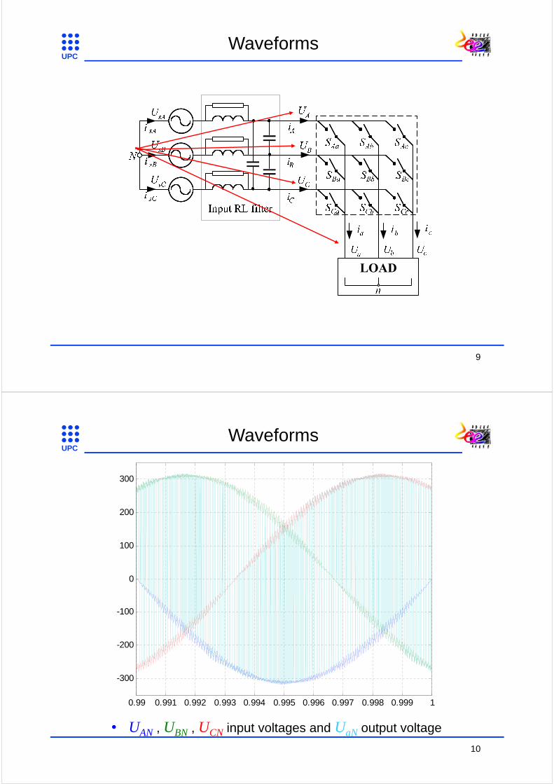
Waveforms
UPC
10
0.99 0.991 0.992 0.993 0.994 0.995 0.996 0.997 0.998 0.999 1
-300
-200
-100
0
100
200
300
• UAN , UBN , UCN input voltages and UaN output voltage
Waveforms

UPC
11
0.99 0.9901 0.9902
-300
-200
-100
0
100
200
300
• UAN , UBN , UCN input voltages and UaN output voltage
Waveforms
UPC
12
Waveforms
• Uan = 2/3 UaN -1/3 UbN -1/3 UcN = UaN + UNn
• UNn = -1/3 (UaN + UbN + UcN )

UPC
13
Waveforms
0.994 0.995 0.996 0.997 0.998 0.999 1-400
-300
-200
-100
0
100
200
300
400
• Uan output voltage
UPC
14
Waveforms
• Uab = f ( UAB ,UAC ,UBC ,UBA ,UCA ,UCB )

UPC
15
0.98 0.982 0.984 0.986 0.988 0.99 0.992 0.994 0.996 0.998 1-600
-400
-200
0
200
400
600
• UAB , UAC , UBC , UBA , UCA , UCB input line voltages
versus Uab output line voltage
Waveforms
UPC
16
0.982 0.9821 0.9822-600
-400
-200
0
200
400
600
• It uses the two largest voltages
Waveforms

UPC
17
Waveforms
UPC
18
0.994 0.995 0.996 0.997 0.998 0.999 1-400
-300
-200
-100
0
100
200
300
400
Uan ia inductive current (small dephase or delay)
Waveforms

UPC
19
Waveforms
UPC
20
0.98 0.982 0.984 0.986 0.988 0.99 0.992 0.994 0.996 0.998 1
-10
-5
0
5
10
Different frequencies isA ia
Waveforms
UPC
21
WaveformsWaveforms
UPC
22
0.98 0.982 0.984 0.986 0.988 0.99 0.992 0.994 0.996 0.998 1
-10
-5
0
5
10
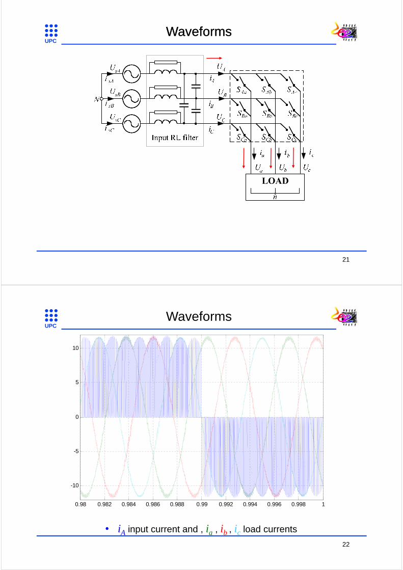
• iA input current and , ia , ib , ic load currents
Waveforms

UPC
23
WaveformsWaveforms
UPC
24
Waveforms
0.98 0.982 0.984 0.986 0.988 0.99 0.992 0.994 0.996 0.998 1
-10
-5
0
5
10
• isA filtered input current and iA non filtered input current
UPC
25
WaveformsWaveforms
UPC
26
0.98 0.982 0.984 0.986 0.988 0.99 0.992 0.994 0.996 0.998 1
-300
-200
-100
0
100
200
300
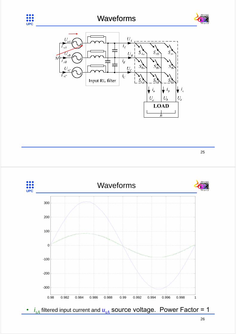
• isA filtered input current and usA source voltage. Power Factor = 1
Waveforms

UPC
27
Waveforms
UPC
28
• UsAN source and UAN input phase voltages
Waveforms
0.98 0.982 0.984 0.986 0.988 0.99 0.992 0.994 0.996 0.998 1
-300
-200
-100
0
100
200
300

UPC
29
Alternatives
• Industry “workhorse” from less than kW to MW• Unidirectional power flow• 2 quadrant
– When the current changes its sign, the power must be burn in the DC link
• DC link capacitor (30% -50% of the power circuit volume)
• Input currents very poor. (awful THD)
UPC
30
Alternatives
• Bi directional power flow• 4 quadrant• DC link capacitor and input inductors• Sinusoidal input currents. Input Power Factor 1• Matrix Converter real alternative
N
San
Sap
Sbn
Sbp Scp
Scn
ia
ic
ib
a
b
c
SBp SCp
A
BC
SAp
SBn SCnSAn

UPC
31
MC versus back to back
• 12 IGBTs + 12 Diodes• 1 large electrolytic capacitor (DC link) • Input filter (1st order)
– 3 large inductors
• 18 IGBTs + 18 Diodes• Input filter (2nd order)
– 3 inductors– 3 capacitors
• Clamp circuit
Ua U U
UC
UB
UA
b c
icibia
SAa SAb SAc
SBa SBb SBc
SCa SCb SCc
iA
iB
iC
T2
D2
T1
D1
N
San
Sap
Sbn
Sbp Scp
Scn
ia
ic
ib
a
b
c
SBp SCp
A
BC
SAp
SBn SCnSAn
UPC
32
D1
T1
D2
D3D4
Bi Directional Switch
• Diode embedded switch– Switch: 1 IGBT + 4 diodes– Conducting losses: 2 diodes +1 IGBT
• Back to back switch with common collector– Switch: 2 IGBT + 2 diodes– Diode required for reverse blocking capability– Conducting losses: 1 diode +1 IGBT
• Back to back switch with common emitter– Switch: 2 IGBT + 2 diodes– Diode required for reverse blocking capability – Conducting losses: 1 diode +1 IGBT
T2
D2
T1
D1
T2
D2
T1
D1
• Must be able to conduct positive and negative current and block positive and negative voltage

UPC
33
Bi Directional Switch
SUMMARY IGBTs DiodesIsolated Power
SuppliesConducting
DevicesDiode bridge 9 36 9 3
Common Emitter 18 18 9 2
Common Collector 18 18 6 2
T2
T1
• Reverse Blocking IGBT, RBIGBT– Two reverse blocking IGBTs– Lower conducting losses: one switching device– Still under research– Switch control will remain the same
UPC
34
Bi Directional Switch Device Packaging
• Dynex 200 (A) Bi directional Module– From standard one leg conventional VSI – 9 for a 3x3MC– Large Converters > 200 (A)– Common collector
LOAD
Va Vb Vc
T2
D2
T1
D1

UPC
35
…Dynex Semiconductor is working closely with researchers at Nottingham University. Through this collaboration and in response to commercial requirements, Dynex has created the DIM400PBM17-A000 for use in a 60Hz to 400Hz fixed frequency converter and the GP200MBS12 for use in a high efficiency brushless dc motor drive. The DIM400PBM17-A000 module is a 400A 1700V bi-directional switch mounted on a 140mm x 73mm metal matrix baseplate. Long-term reliability and enhanced thermal performance are achieved through the use of aluminium nitride substrates mounted on a metal matrix compound baseplate. The package has a 6 kV isolation rating…
….announced the release of two bi-directional IGBT modules for use in matrix converter power stages…
…The DIM200MBS12-A000 module is a 200A 1200V bi-directional switch mounted on a 106mm x 62mm copper baseplate. The package has a 4 kV isolation rating…
http://www.dynexsemi.com/corporate/news/items/20020514-prod-b.htm
Bi Directional Switch Device Packaging
UPC
36
Bi Directional Switch Device Packaging
• SEMELAB 200 (A) Bi directional Module– 3 for a 3x3MC– Large Converters
LOAD
Va Vb Vc

UPC
37
A Matrix Converter IGBT Bi-Directional switching moduleA 360kVA (600V max line-line at up to 300A) matrix converter module designed by Semelab.•IGBT Packaging Available in 300V to 1800V •Aerospace •Customised to fit your needs. •Good CTE match, from Silicon to the metal matrix base plate. •Excellent reliability module, temp cycling, humidity tested, elevated pressure. •Low power losses. •Plastic package / Hermitic packaging •Power connection, •Mounting holes •Void free die attach, X-ray capability.
Bi Directional Switch Device Packaging
http://www.semelab.co.uk/power/
UPC
38
Full Matrix Converter Device Packaging
• EUPEC 35A Matrix Converter Module– 1 for a 3x3MC– Small Powers Converters. 7.5 kW
LOAD
Va Vb Vc

UPC
39
Full Matrix Converter Device Packaging
UPC
40
Full Matrix Converter Device Packaging
• Fuji Electric Device Technology Co.,Ltd.– 1 for a 3x3MC– Four options (Price 390 € Nov 2009) :
• 1200V 50A 1200V 100A• 600V 100A 600V 200A

UPC
41
Full Matrix Converter Device Packaging
• 600V 200A
• 1200V 100A
• 1200V 50A
• 600V 100A
UPC
42
Commutation
• Current commutation– Needs the sign of the output current per phase
• Add two anti parallel diodes and measure its voltage drops
• Measure the device voltage drops
– Most widely used
• Voltage commutation– Needs the input voltage values per phase
T2
D2
T1
D1
T2
D2
T1
D1
VA
Va
D6
D5
T2
D2
T1
D1

UPC
43
4 Step Current Commutation
T4
T3
D3
T2
D2
T1
D1
VB
VA
Va
D4
T2
T3
Va
t d1
VA
T1
T4
Va
t d2t c
ideal
T2
T3
Va
T1
T4
Va
ideal
t d1
VB
t d2t c
t rt f
VB VAVA VB
I a > 0
VA VB>
realreal
• No short circuits at the input• No open circuit at the output
(inductive loads)
UPC
44
T2
T3
Va
t d1
VA
T1
T4
t d2t c
ideal
T2
T3
Va
T1
T4
ideal
t d1
VB
t d2t c
t ft r
VB VAVA VB
I a < 0
Va V
a
VA VB>
realreal
T4
T3
D3
T2
D2
T1
D1
VB
VA
Va
D4
4 Step Current Commutation

UPC
45
Matrix Converter
EUPEC FM35R12KE3ENG module
Switching device 1200V, 35 A, IGBT
td1 / tc / td2 1 / 0.2 / 0.5 s
tf / tr 65-90 ns / 30-45 ns
Power 7.5 kW
AC Input voltage 3 x 415V
Input filter (L/C) values 1mH / 1.5F
4 Step Current Commutation
UPC
46
Input Filter
• 2nd Order Input L-C filter– Typical cut off frequency 1-3 kHz
• between the fundamental 50Hz • and the PWM frequency 10-20 kHz
– R in parallel with L in order to have an adequate damping– L impedance at 50Hz should be negligible
• 2*pi*f*L = 2*3.14*50*10-3 = 0.314 ohms
Matrix Converter
EUPEC FM35R12KE3ENG module
Switching device 1200V, 35 A, IGBT
Power 7.5 kW
AC Input voltage 3 x 415V
Input filter (L/C) values 1mH / 1.5F
LOAD
VB
VA
VC
Va Vb Vc

UPC
47
Clamp circuit
LOAD
VB
VA
VC
Va Vb Vc
• Diode bridge like a standard rectifier• Protection against
– open circuits with inductive currents– over voltage caused by transients in power up and voltage sags
UPC
48
MC Output Voltage vectors
• Space Vector Concept: 34
32
32 j
cj
bao etUetUtUtU
State +1Ua=UA Ub=UB Uc=UB
Ua=ÛA cos (30º)Ub=ÛB cos (-90º)Uc=ÛB cos (-90º)
Ua=ÛA cos(0º)Ub=ÛB cos(-120º)Uc=ÛB cos(-120º)
Ua=ÛA cos(-30º)Ub=ÛB cos(-150º)Uc=ÛB cos(-150º)

UPC
49
inpu
t vol
tage
s (
V )
MC Output Voltage vectors
• Variable amplitude
• Same angle
UPC
50
MC Input Current vectors
cos(30º) = sqr(3)/22/3·2·cos(30º) = 2/sqr(3)
• Space Vector Concept: 34
32
32 j
Cj
BAi etietititi
State +1iA = ia iB=ib+ic iC=0
aA
B
C
b c a
a -30º
• Amplitude dependant on the load• Same angle

UPC
51
oV
ii
a b c o i
+1 A B B 2/3UAB 0 2/sqr(3) ia 11/6
+2 B C C 2/3UBC 0 2/sqr(3) ia /2
+3 C A A 2/3UCA 0 2/sqr(3) ia /6
+4 B A B 2/3UAB 2/3 2/sqr(3) ib 11/6
+5 C B C 2/3UBC 2/3 2/sqr(3) ib /2
+6 A C A 2/3UCA 2/3 2/sqr(3) ib /6
+7 B B A 2/3UAB 4/3 2/sqr(3) ic /6
+8 C C B 2/3UBC 4/3 2/sqr(3) ic /2
+9 A A C 2/3UCA 4/3 2/sqr(3) ic /6
+R1 A B C U [U] io MAX [io MAX]
+R2 C A B U [U +2/3] io MAX [io MAX+2/3]
+R3 B C A U [U +4/3] io MAX [io MAX+4/3]
0A A A A 0 …. 0 ….
0B B B B 0 …. 0 ….
0C C C C 0 …. 0 ….
a b c o i
-1 B A A -2/3UAB 0 -2/sqr(3) ia 11/6
-2 C B B -2/3UBC 0 -2/sqr(3) ia /2
-3 A C C -2/3UCA 0 -2/sqr(3) ia /6
-4 A B A -2/3UAB 2/3 -2/sqr(3) ib 11/6
-5 B C B -2/3UBC 2/3 -2/sqr(3) ib /2
-6 C A C -2/3UCA 2/3 -2/sqr(3) ib /6
-7 A A B -2/3UAB 4/3 -2/sqr(3) ic /6
-8 B B C -2/3UBC 4/3 -2/sqr(3) ic /2
-9 C C A -2/3UCA 4/3 -2/sqr(3) ic /6
-R1 A C B U [- U] io MAX [-io MAX]
-R2 B A C U [- U +2/3] io MAX [-io MAX+2/3]
-R3 C B A U [- U +4/3] io MAX [-io MAX+4/3]
oV
ii
27 vectors: 18 constant in direction + 3 nulls + 6 rotating
MC Output Voltage & Input Current vectors
Where, U equals to 2/3·cos(30º)· ÛL
UPC
52
MC Output Voltage & Input Current vectors
Kv=3
Kv=4
Kv=5
Kv=2
Kv=6vo’’
vo’0
~
vo
9,8,7
9,8,7
3,2,1 3,2,1
6,5,4
6,5,4 Ki=3
Ki=4
Ki=5
Ki=2
Ki=6
ii’’
ii’
0
~ii
7,4,1
7,4,1
9,6,3
9,6,3
8,5,2
8,5,2

UPC
53
Modulation
• PWM Modulation technique is applied in order to:– follow a reference at the output, which on average will be a
sinusoidal
– get sinusoidal input currents on phase with the input voltage
(power factor 1)
• Several modulation techniques:– Venturini, Scalar…
• Direct & Indirect Space Vector Modulation– Based on the Space Vector Modulation for Standard PWM
Inverters– There are two references:
• Output voltage vector• Input current angle
UPC
54
Kv=3
Kv=4
Kv=5
Kv=2
Kv=6vo’’
vo’0
~
vo
• Output voltage vector:
0v
''
0
'
00 vvv
• The voltage reference vector will be synthesized using adjacent vectors :
Direct Space Vector Modulation
Reference 1

UPC
55
• Input current angle:
where usually:
0
~
• The input current angle will be obtained distributing the load current among adjacent vectors in the right proportions:
Direct Space Vector Modulation
Reference 2
Ki=3
Ki=4
Ki=5
Ki=2
Ki=6
ii’’
ii’
0
~ii
vi
i
0i
'''
iii iii
UPC
56
Direct Space Vector Modulation
3~cos
3
2~3
cos3
2
~3
cos2
3
~66
cos6
cos
0000'0
00'0
00'0
vvv
vv
vvy
6~
6 0
6~
00
33
1
00'0 3
~cos3
2
vKj
evv
''
0
'
00 vvv 0
~
Reference 1, output voltage vector:

UPC
57
3~cos
3
2
~3
cos2
3
~66
cos6
cos
00''
0
00''
0
00''
0
vv
vv
vvx
3
1
00''
0 3~cos
3
2
vKj
evv
6~
6 0
6~
00
0~
''
0
'
00 vvv
Direct Space Vector Modulation
UPC
58
Kv=3
Kv=4
Kv=5
Kv=2
Kv=6vo’’
vo’0
~
vo
9,8,7
9,8,7
3,2,1 3,2,1
6,5,4
6,5,4
• What vectors can be used?– Maximum input voltages at Ki=1 : UAB, UAC.
– Common vectors For Kv=1 & Ki=1: • ±1 (± 2/3 UAB) ±3 (± 2/3 UCA)
• ±7 (± 2/3 UAB) ±9 (± 2/3 UCA)
– Using just 2 vectors, both references can not be fulfilled => 4 active vectors will be used
Ki=3
Ki=4
Ki=5
Ki=2
Ki=6
ii’’
ii’
0
~ii
7,4,1
7,4,1
9,6,3
9,6,3
8,5,2
8,5,2
UCUBUA
UAC UBC UBA UCA UCB UAB
1 12 3 4 5 6input sector
Direct Space Vector Modulation

UPC
59
vo’
voI · I
voII· II
vo’’
voIII· III vo
IV· IV
''
0
'
00 vvv II
II
oI
I
o vvv ··'
0 IV
IV
oIII
III
o vvv ··'
0
II
II
oI
I
o
Kj
vvevvv
··3
~cos3
2 331
00'0
IV
IV
oIII
III
o
Kj
vvevvv
··3
~cos3
2 31
00''
0
o
o
y
x
0~
o
Direct Space Vector Modulation
UPC
60
'''
iii iii
IIIIII
iI
I
ii iii ··'
IVIV
iII
II
ii iii ··'
ii’
iiI · I
iiIII· IIIii’’
iiII · II
iiIV· IV
i~
ii
i~
i
i
0··· 3
1~
ii
KjjIIII
iI
I
i ejeii
0··· 3
1~
ii
KjjIVIV
iIII
III
i ejeii
Direct Space Vector Modulation
Reference 2, input current angle

UPC
61
II
II
oI
I
o
Kj
vvevvv
··3
~cos3
2 331
00'0
IV
IV
oIII
III
o
Kj
vvevvv
··3
~cos3
2 31
00''
0
0··· 3
1~
ii
KjjIIII
iI
I
i ejeii
0··· 3
1~
ii
KjjIVIV
iIII
III
i ejeii
i
i
i
oKKIV
i
i
i
oKKIII
v
v
v
v
iv
iv
cos3
~cos
3~cos
3
21
cos3
~cos
3~cos
3
21
01
0
i
i
i
oKKII
i
i
i
oKKI
v
v
v
v
iv
iv
cos3
~cos
3~cos
3
21
cos3
~cos
3~cos
3
21
0
01
IVIIIIII 10
• Solving the 4 equations, the four duty cycles are found
• The remaining duty is for the zero vectors
Direct Space Vector Modulation
UPC
62
• To obtain a correct balance of the input currents and the output voltages, the modulation pattern should be a combination of all 4 duty-cycles
• And the zero vector is calculated as follows
• The typical modulation pattern is as shown in next slide
ddd ddd ddd ddd
ddddd 10
inImd *
3sin
inImd *sin
outUmd *
3sin
outUmd *sin
Rectification stage Inversion stage
Ref. inputcurrent
Ref. outputvoltage
Indirect Space Vector Modulation

UPC
63
Modulation switching pattern
UPC
64
Modulation switching pattern

UPC
65
-400
-200
0
600
400
200UCUBUA
UAC UBC UBA UCA UCB UAB
1 12 3 4 5 6
input sector
Modulation switching pattern
UPC
66
Modulation switching pattern
UC UAUA UB
δO3 /2 δ 1 /2 δ 3 /2 δO1 /2
UAUC
U aN
δ 2 /2 δ4 /2 δO2 /2
UB
δO2 /2
UB
δ4 /2 δ2 /2 δO1 /2
UA
δ 3 /2 δ 1 /2
UC
δ O3 /2
UB UAUA UC
Input sector 1. Input angle +30º
UNn
Uan
U
U
U bN
U cN
bn
cn
2/3·0.87
-0.87
0.87-0.87
0.87-0.87
0.87
1/3·0.87-1/3·0.87-2/3·0.87
0.871/3·0.87-1/3·0.87-2/3·0.87
-0.87
-1/3·0.87-2/3·0.87-4/3·0.87
4/3·0.872/3·0.871/3·0.87
Output sector 1. Output angle +30º
-3 +9 -7 +1 +1 -7 +9 -3

UPC
67
+
- LOADLOADLOAD
VB
VA
VC
Va Vb Vc
VI T4
T3
D3
T2
D2
T1
D1
VB
VA
Va
D4
T2
D2
T1
D1VA
Va
Ii
VDi
Voltage Drop effect
General scheme
Matrix Converter linearization
Matrix Converter linearization
UPC
68
Four step commutation
(td1 + tc + td2 = 1µs+0.2µs+0.5µs)
T2
T3
Va
t d1
VA
T1
T4
Va
t d2t c
ideal
T2
T3
Va
T1
T4
Va
ideal
t d1
VB
t d2t c
t rt f
VB VAVA VB
I a > 0
VA VB>
realreal
T4
T3
D3
T2
D2
T1
D1
VB
VA
Va
D4
Voltage Edge Uncertainty effect
Matrix Converter linearization
Matrix Converter linearization

UPC
69
I a
I b
VC VA
I c
VA VB
δO3/2 δ1/2 δ3/2 δO1/2
VAVC
Va ideal
Va
> 0
Vb ideal
Vb
< 0t ft d1+ tc +
Vc ideal
Vc
< 0t ft d1+ tc +
δ2/2 δ4/2 δO2/2
VB
t ft d1+ tc +t rt d1 +
t rt d1+
t rt d1 +
δO2/2
VB
δ4/2 δ2/2 δO1/2
VA
δ3/2 δ1/2
VC
δO3/2
=VB VA
VA VC
t rt d1+ t ft d1+ tc +
t ft d1+ tc + t rt d1+
t ft d1+ tc + t rt d1+
SECTOR 1
TPWM
real
real
real
Model for Voltage Edge Uncertainty effect
SVM
V
I
-VEU
+VEU
Matrix Converter linearization
Matrix Converter linearization
UPC
70
V
I
V
I
-VEU
+VEU
V
I
-VEU
+V EU+Ic
-Ic
input: phasecurrent
output:compensatingphase voltage
Voltage Drop effect
Voltage Edge Uncertainty effect
Dual Compensation
DUAL COMPENSATION
Matrix Converter linearization

UPC
71
SVMMatrix
Converter
DualCompensation
Grid
LC filter
Ia
Ib
Ic
VA
VB
VC
V
V
3 / 2
+
++
+
PMSM
32d q
Iq* +
d-axis currentcontroller
q-axis currentcontroller
+Id*
-
-d q
Ia
Ib
Ic
VdcompaVdcompc
Vdcompb
VdcompVdcomp
Dual Compensation in Matrix Converters FOC Scheme
0 0.1 0.2 0.3 0.4 0.5 0.6 0.7 0.8 0.9 1-8
-6
-4
-2
0
2
4
6
8
time (s)
Va,
Vb
, Vc
(V)
0 0.1 0.2 0.3 0.4 0.5 0.6 0.7 0.8 0.9 1-10
-8
-6
-4
-2
0
2
4
6
8
10
time (s)
Va,
Vb,
Vc
(V)
0 0.1 0.2 0.3 0.4 0.5 0.6 0.7 0.8 0.9 1-0.3
-0.2
-0.1
0
0.1
time (s)
Id (
A)
0 0.1 0.2 0.3 0.4 0.5 0.6 0.7 0.8 0.9 1-0.3
-0.2
-0.1
0
0.1
time (s)
Id (
A)
Matrix Converter linearization
UPC
72
Summary
• Matrix Converter topology– 9 Bidirectional switch
• 4 step commutation• Space Vector Modulation• Input Filter• Clamp Circuit• Matrix Converter linearization• Advantages of Matrix Converters:
– Size. Compactness.– Sinusoidal input/output– Hostile environments– 4 quadrant
• Applications