Embed Size (px)
Citation preview
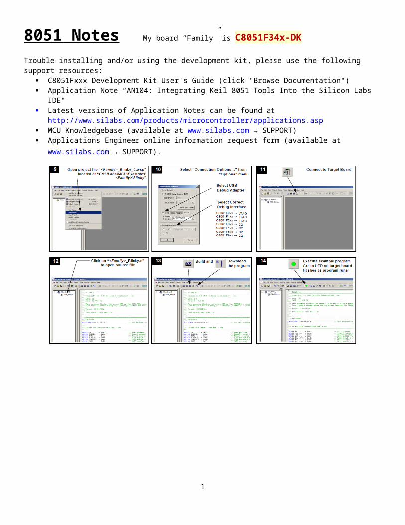
8051 Notes My board “Family” is C8051F34x-DK
Trouble installing and/or using the development kit, please use the following support resources: C8051Fxxx Development Kit User's Guide (click "Browse Documentation") Application Note “AN104: Integrating Keil 8051 Tools Into the Silicon Labs IDE" Latest versions of Application Notes can be found at
http://www.silabs.com/products/microcontroller/applications.asp MCU Knowledgebase (available at www.silabs.com → SUPPORT) Applications Engineer online information request form (available at www.silabs.com → SUPPORT).
1
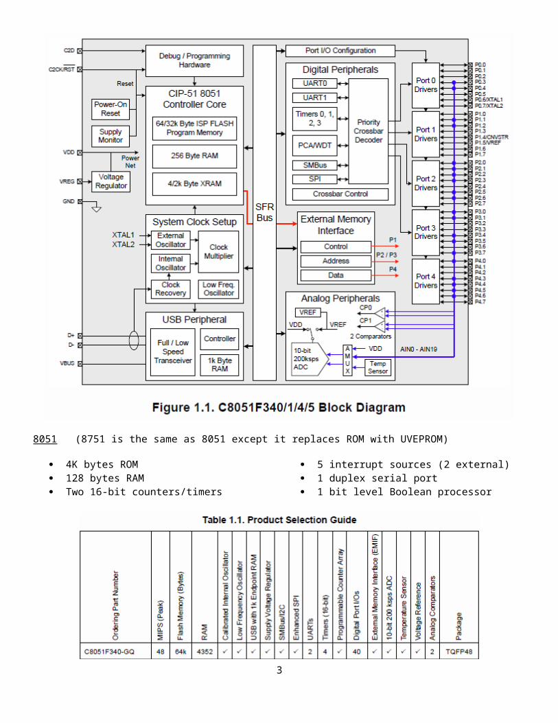
8051 (8751 is the same as 8051 except it replaces ROM with UVEPROM)
4K bytes ROM 128 bytes RAM Two 16-bit counters/timers
5 interrupt sources (2 external) 1 duplex serial port 1 bit level Boolean processor
2
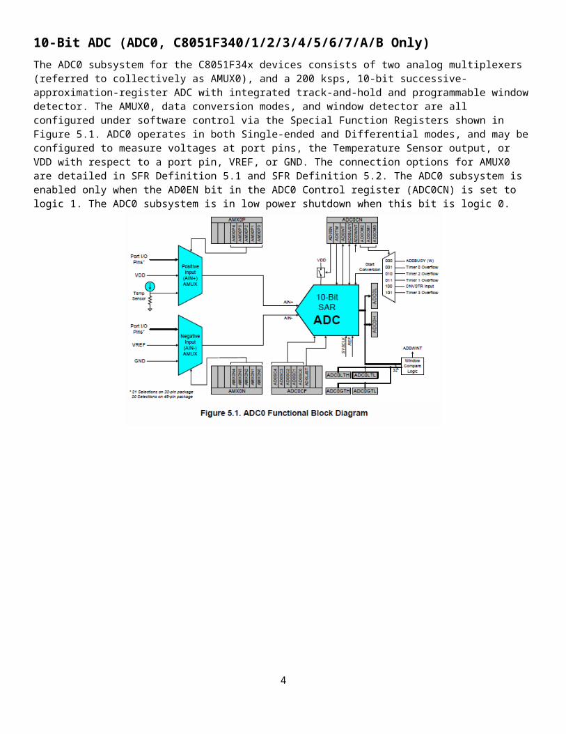
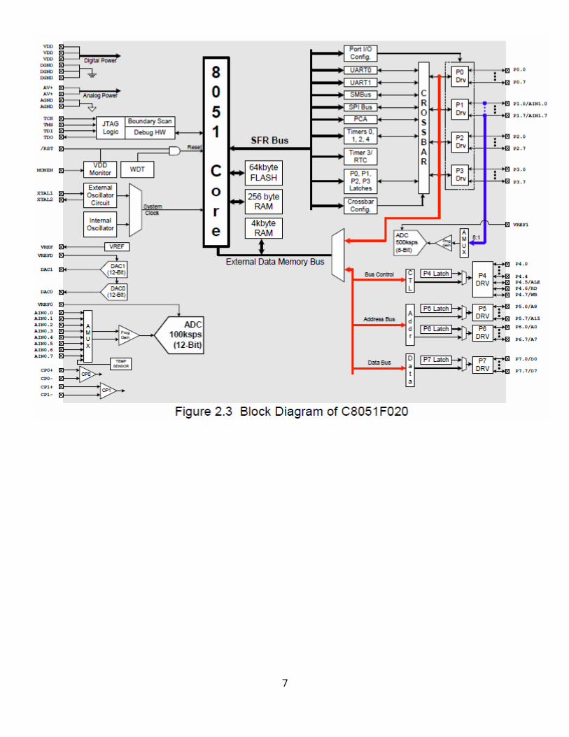
10-Bit ADC (ADC0, C8051F340/1/2/3/4/5/6/7/A/B Only)The ADC0 subsystem for the C8051F34x devices consists of two analog multiplexers (referred to collectively as AMUX0), and a 200 ksps, 10-bit successive-approximation-register ADC with integrated track-and-hold and programmable window detector. The AMUX0, data conversion modes, and window detector are all configured under software control via the Special Function Registers shown in Figure 5.1. ADC0 operates in both Single-ended and Differential modes, and may be configured to measure voltages at port pins, the Temperature Sensor output, or VDD with respect to a port pin, VREF, or GND. The connection options for AMUX0 are detailed in SFR Definition 5.1 and SFR Definition 5.2. The ADC0 subsystem is enabled only when the AD0EN bit in the ADC0 Control register (ADC0CN) is set to logic 1. The ADC0 subsystem is in low power shutdown when this bit is logic 0.
3
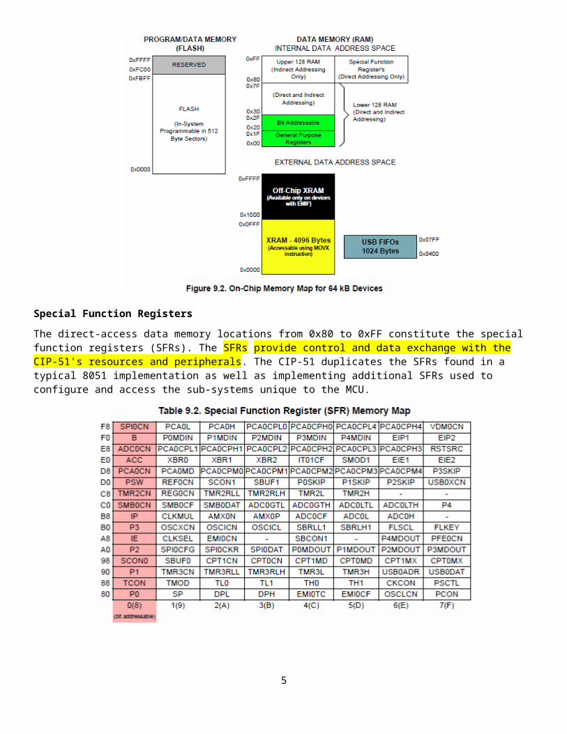
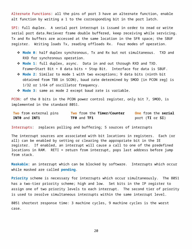
Special Function Registers The direct-access data memory locations from 0x80 to 0xFF constitute the special function registers (SFRs). The SFRs provide control and data exchange with the CIP-51's resources and peripherals. The CIP-51 duplicates the SFRs found in a typical 8051 implementation as well as implementing additional SFRs used to configure and access the sub-systems unique to the MCU.
4
5
6
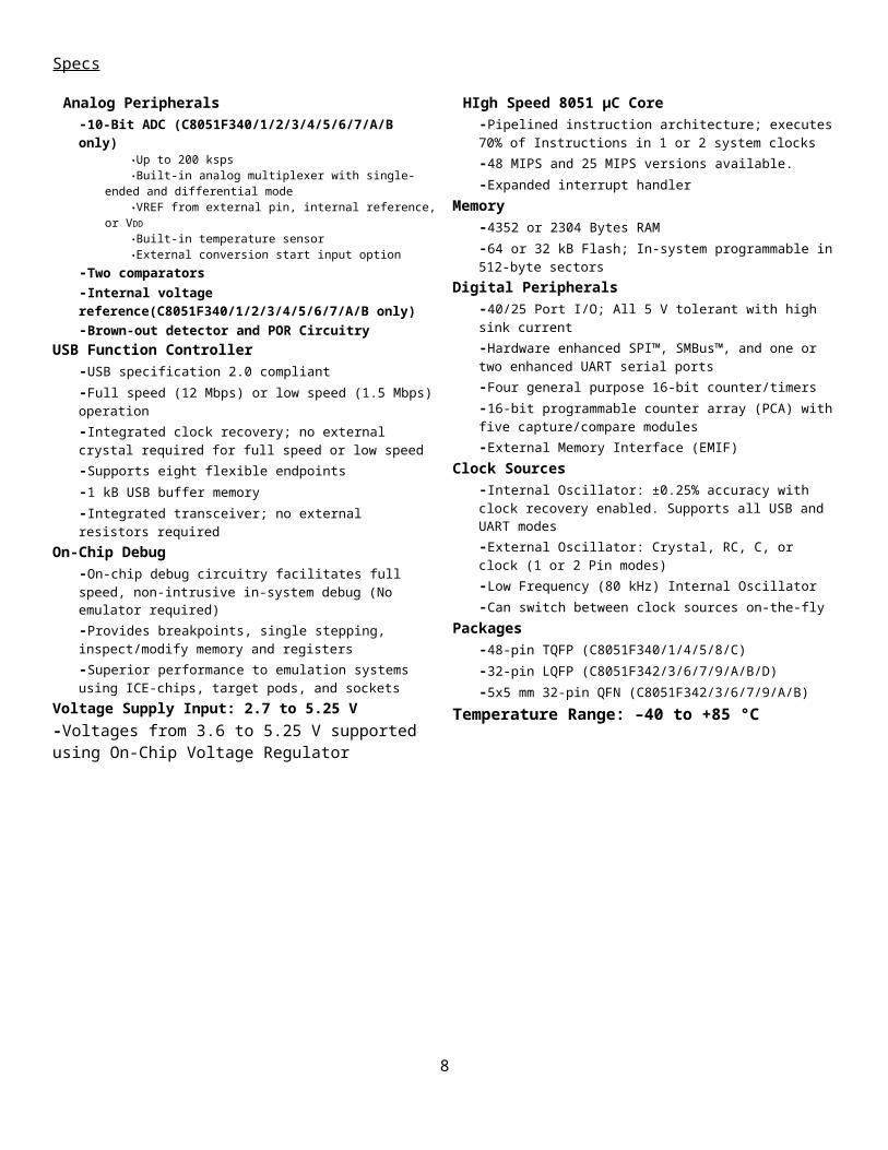
Specs
Analog Peripherals-10-Bit ADC (C8051F340/1/2/3/4/5/6/7/A/B only)
•Up to 200 ksps•Built-in analog multiplexer with single-ended and
differential mode•VREF from external pin, internal reference, or VDD•Built-in temperature sensor•External conversion start input option
-Two comparators-Internal voltage reference(C8051F340/1/2/3/4/5/6/7/A/B only)-Brown-out detector and POR Circuitry
USB Function Controller-USB specification 2.0 compliant-Full speed (12 Mbps) or low speed (1.5 Mbps) operation-Integrated clock recovery; no external crystal required for full speed or low speed-Supports eight flexible endpoints-1 kB USB buffer memory-Integrated transceiver; no external resistors required
On-Chip Debug-On-chip debug circuitry facilitates full speed, non-intrusive in-system debug (No emulator required)-Provides breakpoints, single stepping, inspect/modify memory and registers-Superior performance to emulation systems using ICE-chips, target pods, and sockets
Voltage Supply Input: 2.7 to 5.25 V-Voltages from 3.6 to 5.25 V supported using On-Chip Voltage Regulator
HIgh Speed 8051 μC Core-Pipelined instruction architecture; executes 70% of Instructions in 1 or 2 system clocks-48 MIPS and 25 MIPS versions available.-Expanded interrupt handler
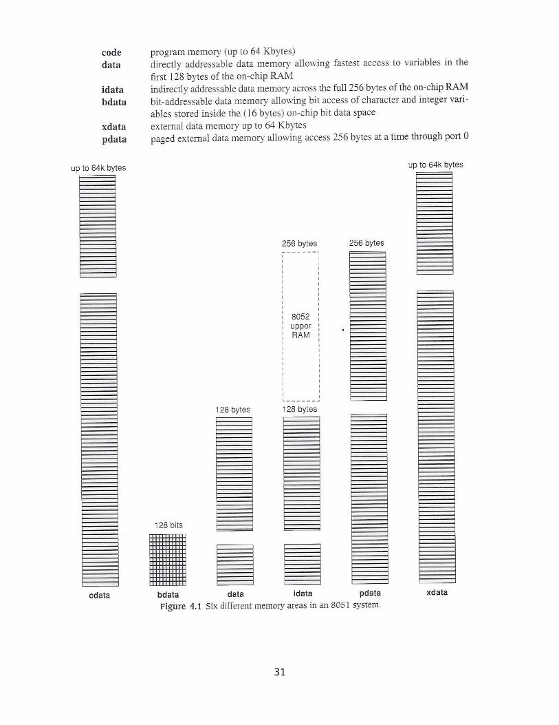
Memory-4352 or 2304 Bytes RAM-64 or 32 kB Flash; In-system programmable in 512-byte sectors
Digital Peripherals-40/25 Port I/O; All 5 V tolerant with high sink current-Hardware enhanced SPI™, SMBus™, and one or two enhanced UART serial ports-Four general purpose 16-bit counter/timers-16-bit programmable counter array (PCA) with five cap-ture/compare modules-External Memory Interface (EMIF)
Clock Sources-Internal Oscillator: ±0.25% accuracy with clock recovery enabled. Supports all USB and UART modes-External Oscillator: Crystal, RC, C, or clock (1 or 2 Pin modes)-Low Frequency (80 kHz) Internal Oscillator-Can switch between clock sources on-the-fly
Packages-48-pin TQFP (C8051F340/1/4/5/8/C)-32-pin LQFP (C8051F342/3/6/7/9/A/B/D)-5x5 mm 32-pin QFN (C8051F342/3/6/7/9/A/B)
Temperature Range: –40 to +85 °C
7
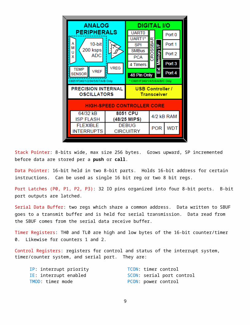
Stack Pointer: 8-bits wide, max size 256 bytes. Grows upward, SP incremented before data are stored per a push or call.
Data Pointer: 16-bit held in two 8-bit parts. Holds 16-bit address for certain instructions. Can be used as single 16 bit reg or two 8 bit regs.
Port Latches (P0, P1, P2, P3): 32 IO pins organized into four 8-bit ports. B-bit port outputs are latched.
Serial Data Buffer: two regs which share a common address. Data written to SBUF goes to a transmit buffer and is held for serial transmission. Data read from the SBUF comes from the serial data receive buffer.
Timer Registers: TH0 and TL0 are high and low bytes of the 16-bit counter/timer 0. Likewise for counters 1 and 2.
Control Registers: registers for control and status of the interrupt system, timer/counter system, and serial port. They are:
IP: interrupt priorityIE: interrupt enabledTMOD: timer mode
TCON: timer controlSCON: serial port controlPCON: power control
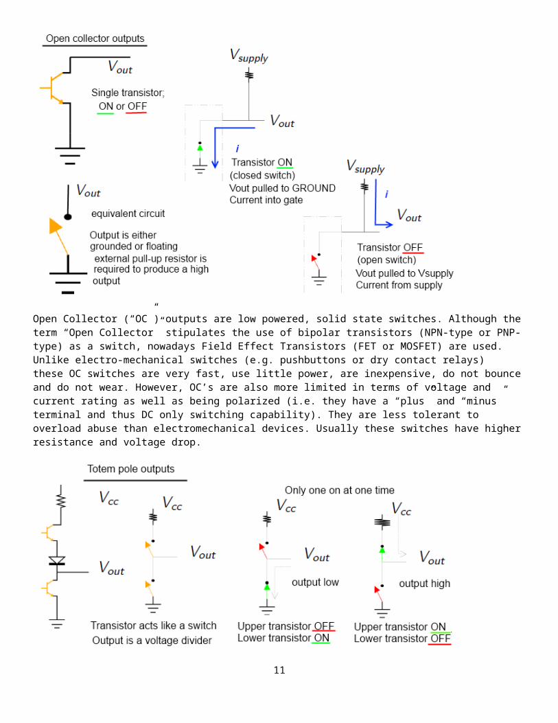
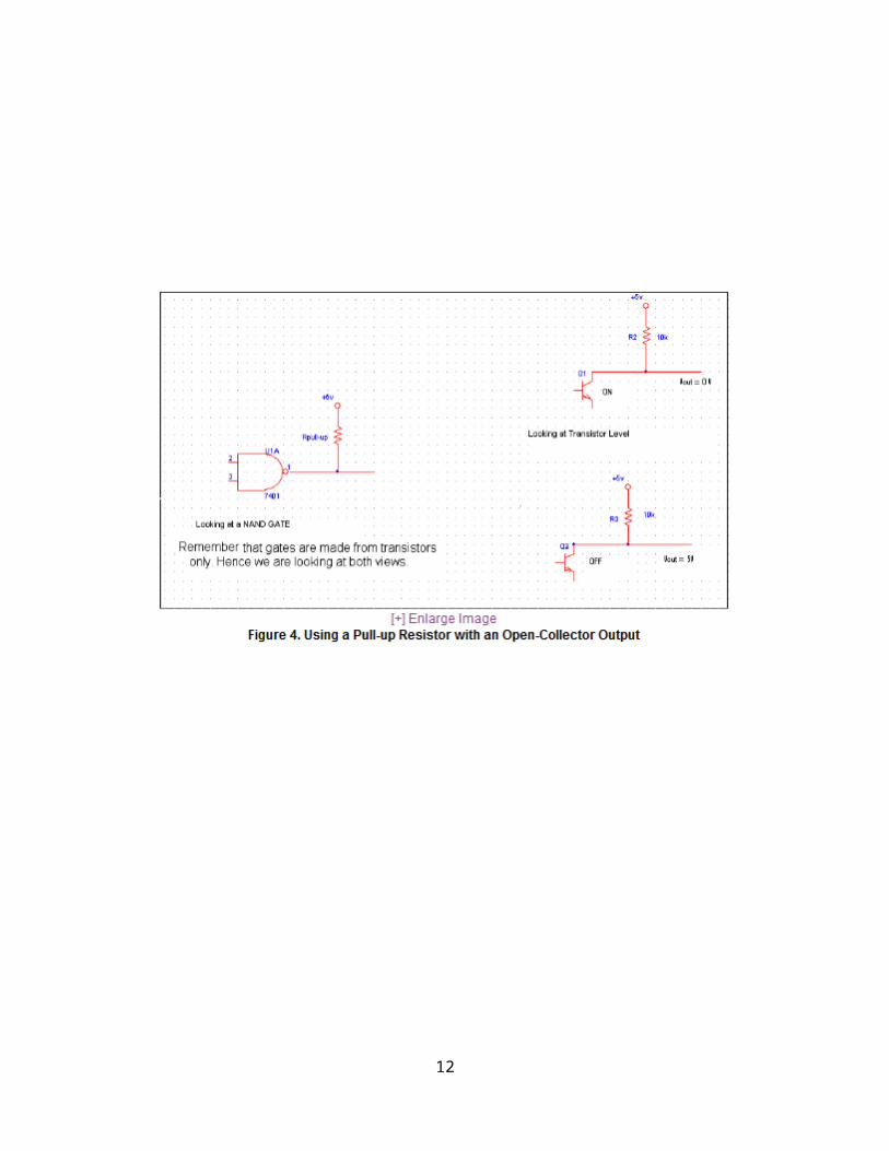
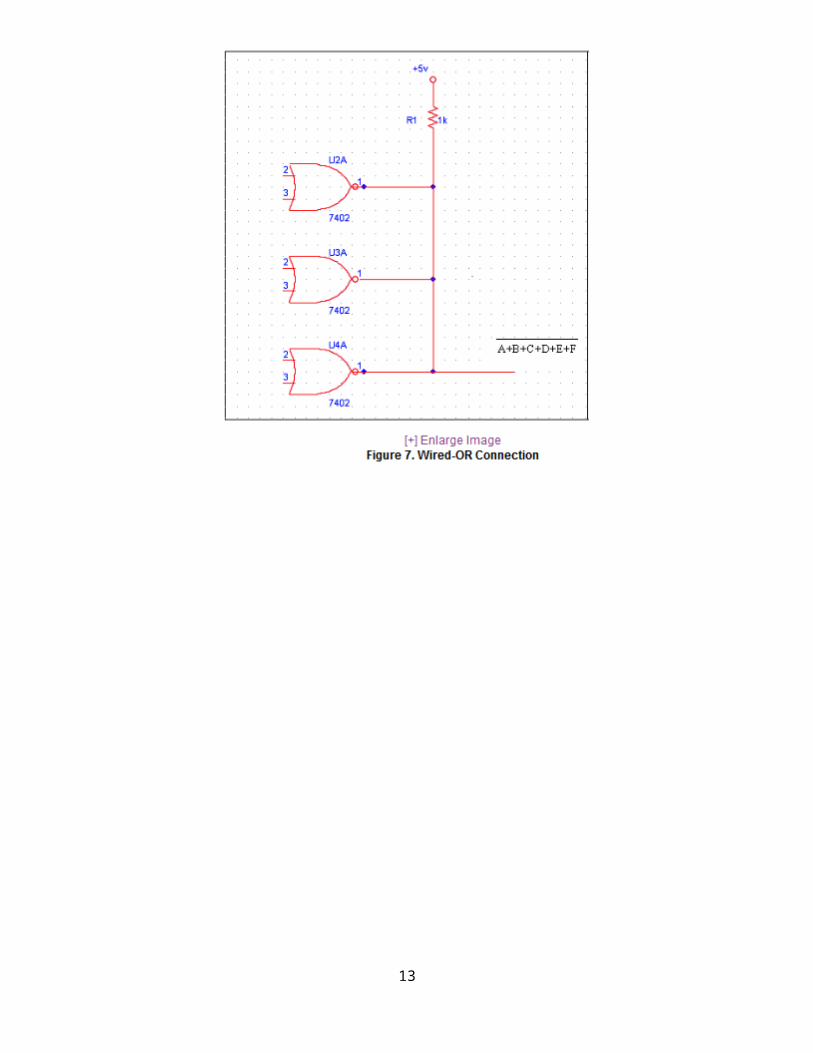
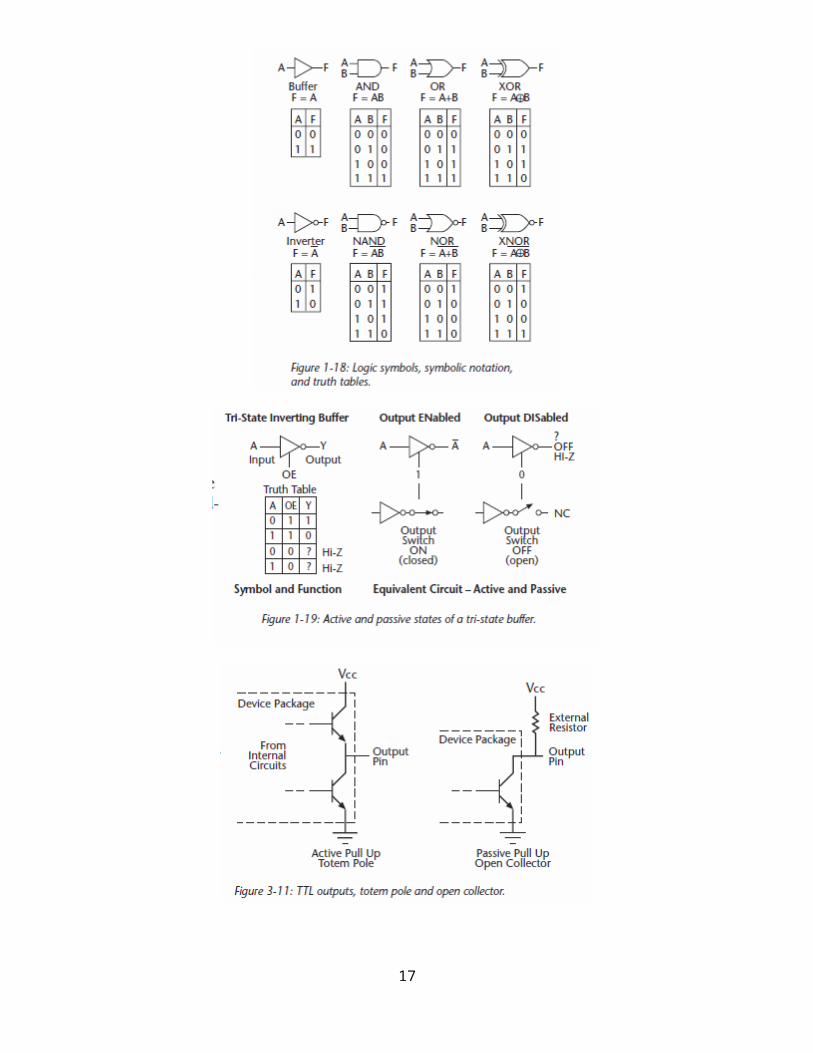
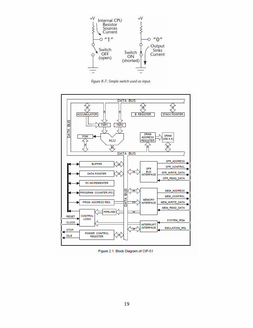
Open Collector / Open Drain
Open-collector/open-drain is a circuit technique which allows multiple devices to communicate bi-directionally on a single wire.
Open-collector/open-drain devices sink (flow) current in their low voltage active (logic 0) state, or are high impedance (no current flows) in their high voltage non-active (logic 1) state. These devices usually operate with an external pull-up resistor that holds the signal line high until a device on the wire sinks enough current to pull the line low. Many devices can be attached to the signal wire. If all devices attached to the wire are in their non-active state, the pull-up will hold the wire at a high voltage. If one or more devices are in the active state, the signal wire voltage will be low.
An open-collector/open-drain signal wire can also be bi-directional. Bi-directional means that a device can both output and input a signal on the wire at the same time. In addition to controlling the state of its pin that is connected to the signal wire (active, or non-active), a device can also sense the voltage level of the signal wire. Although the output of a open-collector/open-drain device may be in the non-active (high) state, the wire attached to the device may be in the active (low) state, due to activity of another device attached to the wire.
The bi-directional nature of an open-collector/open-drain device is what makes this circuit so important in interconnecting many devices on a common line. The I2C Bus and SMBus uses this technique for connecting up to 127 devices.
Open-drain refers to the drain terminal of a MOS FET transistor. Open-collector is the same concept on a bipolar device
8
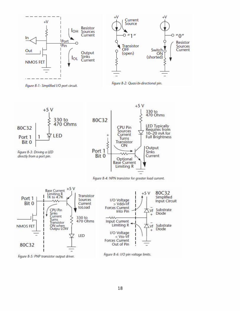
Open Collector (“OC”) outputs are low powered, solid state switches. Although the term “Open Collector” stipulates the use of bipolar transistors (NPN-type or PNP-type) as a switch, nowadays Field Effect Transistors (FET or MOSFET) are used. Unlike electro-mechanical switches (e.g. pushbuttons or dry contact relays)these OC switches are very fast, use little power, are inexpensive, do not bounce and do not wear. However, OC’s are also more limited in terms of voltage and current rating as well as being polarized (i.e. they have a “plus” and “minus” terminal and thus DC only switching capability). They are less tolerant to overload abuse than electromechanical devices. Usually these switches have higher resistance and voltage drop.
9
10
11
12
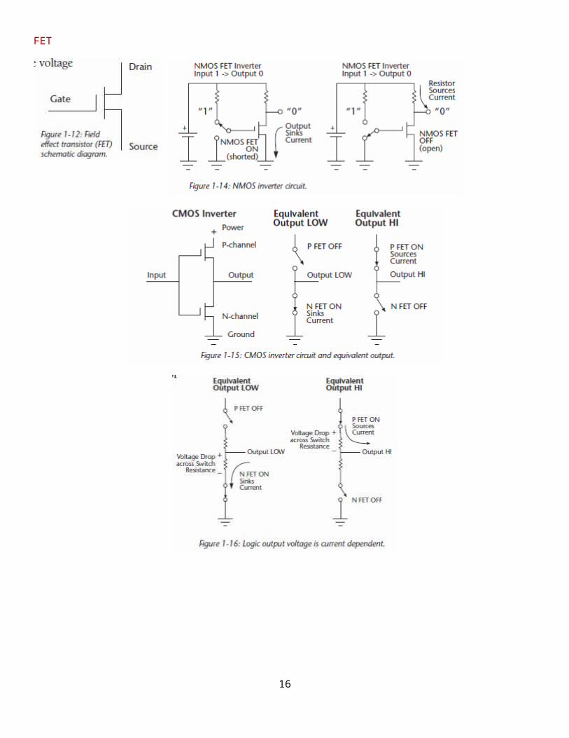
FET
13
14
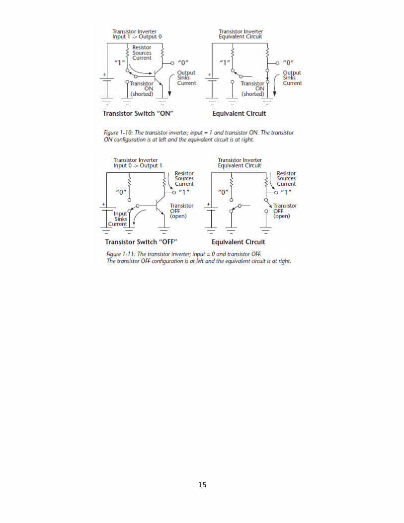
15
16
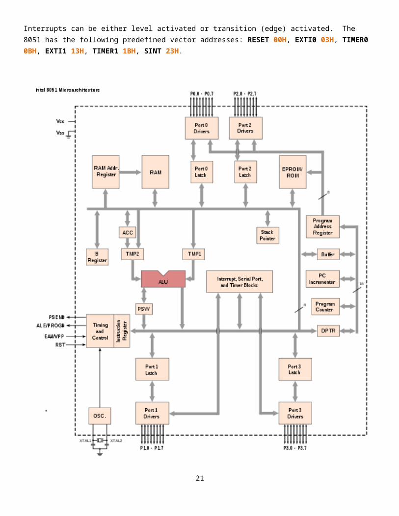
Alternate Functions: all the pins of port 3 have an alternate function, enable alt function by writing a 1 to the corresponding bit in the port latch.
SPI: full duplex. A serial port interrupt is issued in order to read or write serial port data.Reciever frame double buffered, keep receiving while servicing. Tx and Rx buffers are accessed at the same location in the SFR space; the SBUF register. Writing loads Tx, reading offloads Rx. Four modes of operation.
Mode 0: half duplex synchronous, Tx and Rx but not simultaneous. TXD and RXD for synchronous operation.
Mode 1: full duplex, async. Data in and out through RXD and TXD. Frame=Start Bit + 8 data bits + Stop Bit. Interface for data is SBUF.
Mode 2: Similar to mode 1 with two exceptions; 9 data bits (ninth bit obtained from TB8 in SCON), baud rate determined by SMOD [in PCON reg] is 1/32 or 1/64 of oscillator frequency.
Mode 3: same as mode 2 except baud rate is variable.
PCON: of the 8 bits in the PCON power control register, only bit 7, SMOD, is implemented in the standard 8051.
Two from external pins INT0 and INT1 Two from the Timer/Counter TF0 and TF1 One from the serial port (TI or SI)
Interrupts: replaces polling and buffering; 5 sources of interrupts
The interrupt sources are associated with bit locations in registers. Each (or all) can be enabled by setting or clearing the appropriate bit in the IE register. If enabled, an interrupt will cause a call to one of the predefined locations in RAM. RETI = return from interrupt, pops last address before jump from stack.
Maskable: an interrupt which can be blocked by software. Interrupts which occur while masked are called pending.
Priority scheme is necessary for interrupts which occur simultaneously. The 8051 has a two-tier priority scheme; high and low. Set bits in the IP register to assign one of two priority levels to each interrupt. The second tier of priority is used to resolve simultaneous interrupts within the same interrupt level.
8051 shortest response time: 3 machine cycles, 9 machine cycles is the worst case.
Interrupts can be either level activated or transition (edge) activated. The 8051 has the following predefined vector addresses: RESET 00H, EXTI0 03H, TIMER0 0BH, EXTI1 13H, TIMER1 1BH, SINT 23H.
17
18
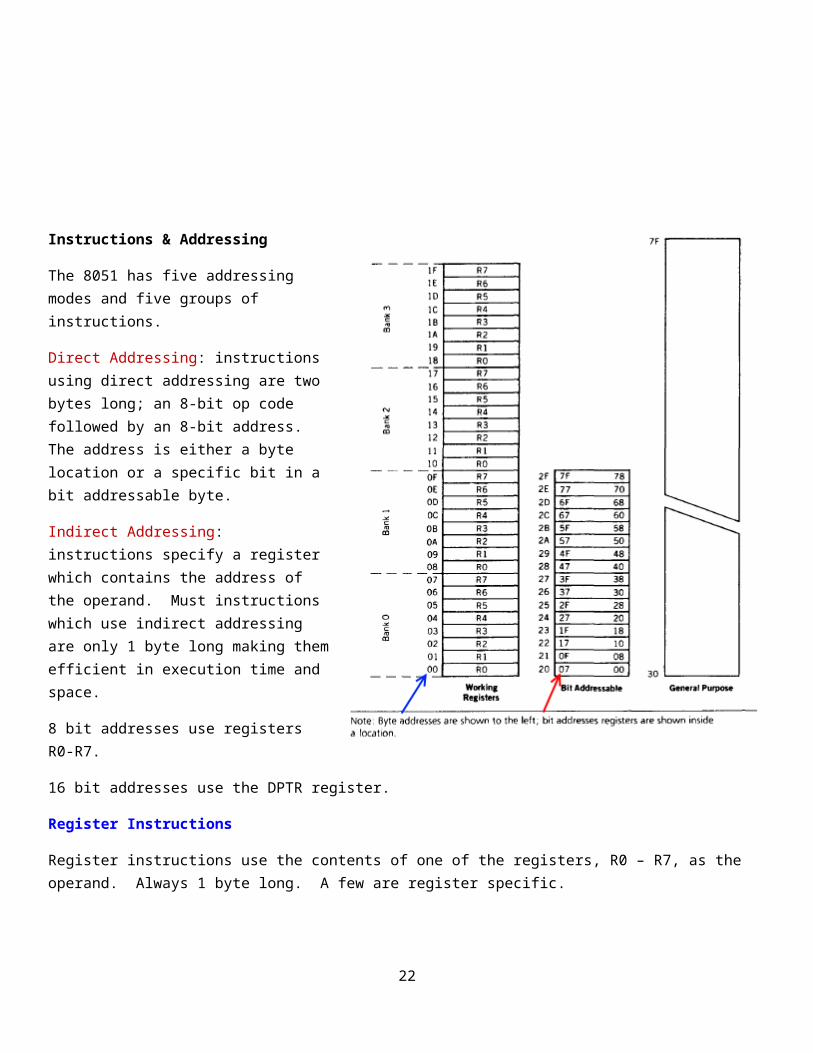
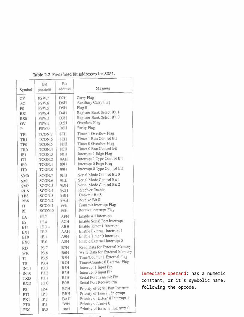
Instructions & Addressing
The 8051 has five addressing modes and five groups of instructions.
Direct Addressing: instructions using direct addressing are two bytes long; an 8-bit op code followed by an 8-bit address. The address is either a byte location or a specific bit in a bit addressable byte.
Indirect Addressing: instructions specify a register which contains the address of the operand. Must instructions which use indirect addressing are only 1 byte long making them efficient in execution time and space.
8 bit addresses use registers R0-R7.
16 bit addresses use the DPTR register.
Register Instructions
Register instructions use the contents of one of the registers, R0 – R7, as the operand. Always 1 byte long. A few are register specific.
19
Immediate Operand: has a numeric constant, or it’s symbolic name, following the opcode.
Index Addressing: two uses; reading data tables from program memory space, implementing jump tables. In each case a 16-bit register holds the base address and the accumulator holds an 8-bit displacement or index. The address of the jump is the sum of the 16-bit base and the 8-bit displacement. Because unsigned, the result is always a forward reference. The base register is either DPTR or PC.
Operand Modifiers: @ before an operand means indirect addressing is being used, # before operand means it is an immediate operand (constant).
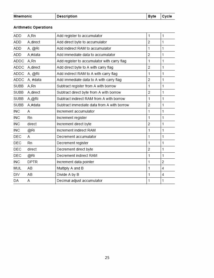
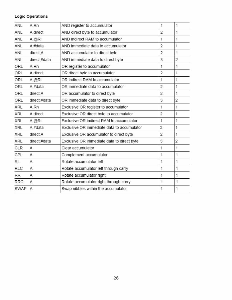
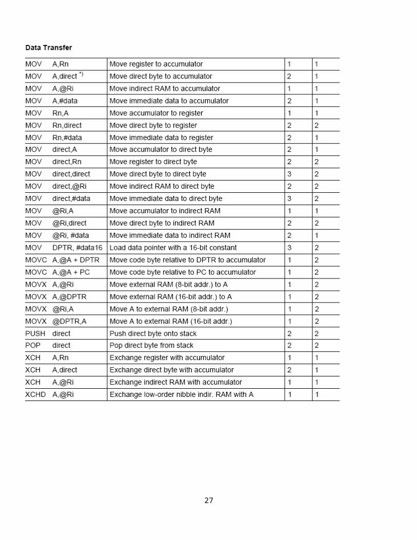
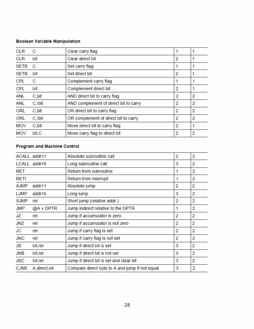
Instruction Groups: arithmetic, logic, data transfer, Boolean, branching.
Instruction Sets:
20
21
22
23
24
Assembler directives are used to define symbols, reserve memory space, store values in program memory and switch between different memory spaces. There are also directives that set the location counter for the active segment and identify the end of the source file.
[refer to “8051 Cross Assembler User's Manual” chapter 5 in 8051 directory for definitions.]
25
26
27
There is no explicit compare instruction, it has been absorbed into a special branching instruction.
Data transfer instructions are compatible with all addressing modes.
The Boolean operators are associated with the 8051 single-bit Boolean processor.
28
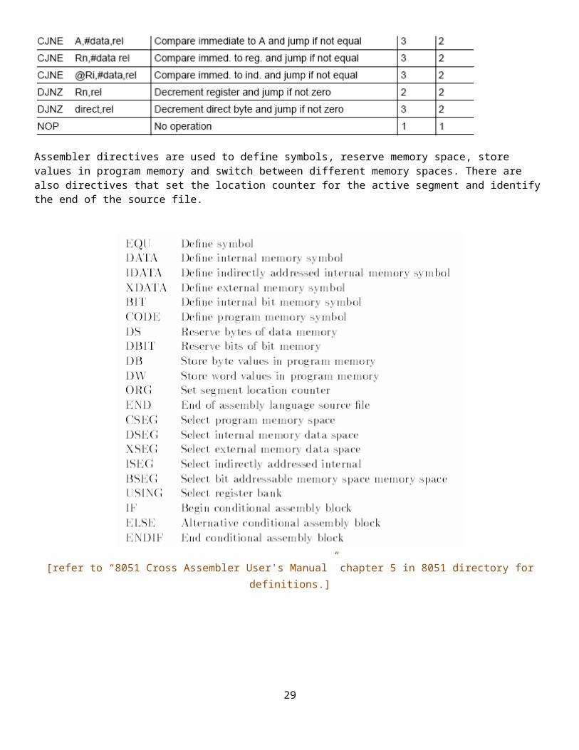
Branching instructions include calls, returns, and various conditional and unconditional jumps.
Conditional jumps are relative to the first byte of the next instruction. Jumps are given as signed twos-compliment 8-bit numbers, the range is -128 to +127 bytes (forward and backwards).
Jumps:
short, relative offset long, 16-bit address, access full memory absolute, 11-bit address, 8 lower bits, 3 upper bits combined with a 5-bit operation specific
CJNE combines the functions of separate compare and jump instructions.
NOP: 1-byte instruction which does nothing, takes one machine cycle. Use for padding delay loops, canbe used to determine pulse width.
Single-Bit Boolean Processor: all port lines as well as 128-bits of RAM and many bits in the SFR register. This is useful in many on-off kinds of control applications such as I/O, switches, lamps, relays, stepper-motor drives, etc.
Carry: The Boolean Accumulator
Bit 7 of the PSW is the carry bit, it is the equivalent of an accumulator for the Boolean processor. Carry bit is known by several names depending on function:
CY: when referring to a bit address.
C: used in register specific instructions which reference the carry bit.
CLR C: one byte register instruction, clears the carry bit.
CLR CY: 2-byte instruction that clears the carry bit by referencing its address in the SFR space.
Bits from SFR register, from internal RAM and from I/O ports, can be read into CY. AND and OR operations can be performed on the CY and result written back to a bit address. Extensive bit manipulation can be done without having to resort to extraneous code.
29

30
31
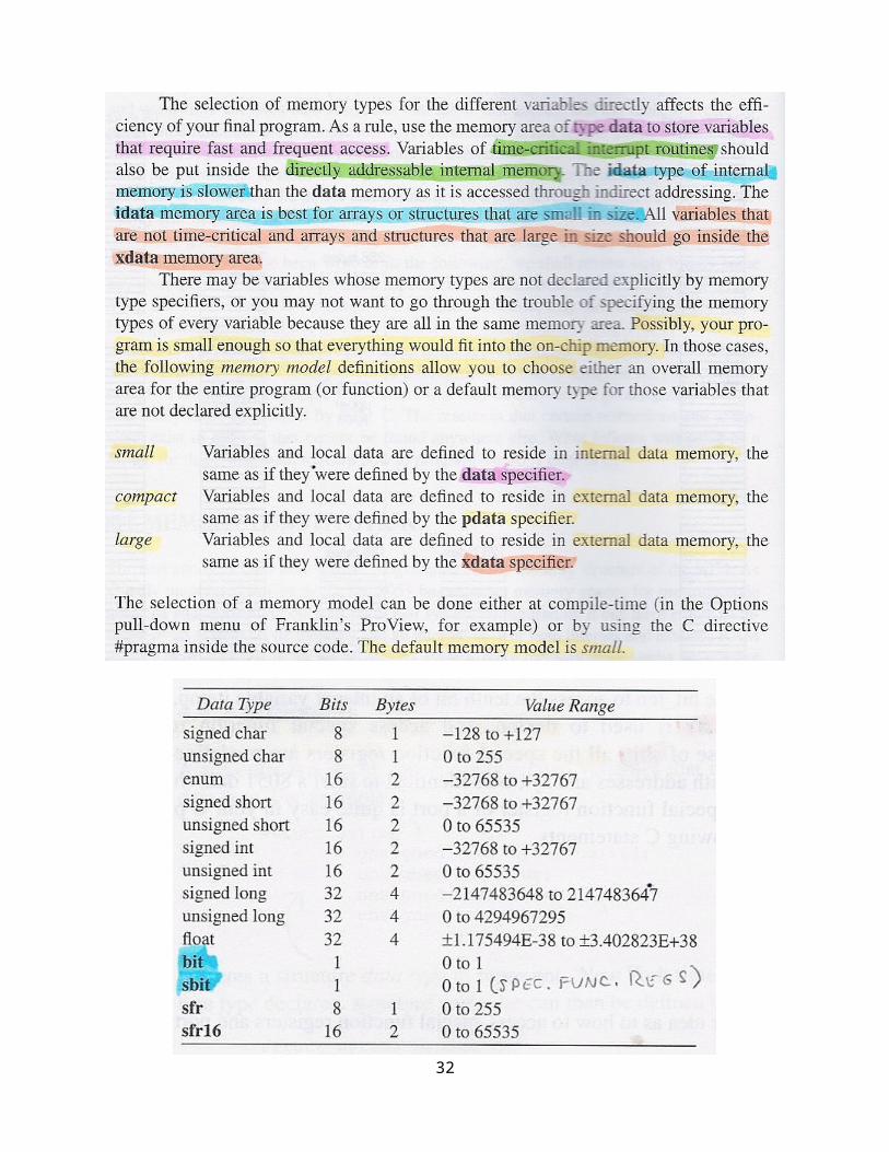
32