Embed Size (px)
Citation preview
Rochester Institute of TechnologyRIT Scholar Works
Theses Thesis/Dissertation Collections
2-22-2014
Novel Metamaterials and Their Applications inSubwavelength Waveguides, Imaging andModulationWangshi Zhao
Follow this and additional works at: http://scholarworks.rit.edu/theses
This Dissertation is brought to you for free and open access by the Thesis/Dissertation Collections at RIT Scholar Works. It has been accepted forinclusion in Theses by an authorized administrator of RIT Scholar Works. For more information, please contact [email protected].
Recommended CitationZhao, Wangshi, "Novel Metamaterials and Their Applications in Subwavelength Waveguides, Imaging and Modulation" (2014). Thesis.Rochester Institute of Technology. Accessed from

R.I.T
NOVEL METAMATERIALS AND THEIR
APPLICATIONS IN SUBWAVELENGTH
WAVEGUIDES, IMAGING AND MODULATION
by
WANGSHI ZHAO
A dissertation submitted in partial fulfillment of the requirements
for the degree of Doctorate of Philosophy in Microsystems Engineering
Microsystems Engineering Program
Kate Gleason College of Engineering
Rochester Institute of Technology
Rochester, New York
FEBRUARY 22, 2014
ii
Novel Metamaterials and Their Applications in Subwavelength
Waveguides, Imaging and Modulation
By
Wangshi Zhao
Committee Approval:
We, the undersigned committee members, certify that we have advised and/or supervised the candidate on
the work described in this dissertation. We further certify that we have reviewed the dissertation manuscript
and approve it in partial fulfillment of the requirements of the degree of Doctor of Philosophy in
Microsystems Engineering.
Dr. Zhaolin Lu _____________________________________________
Committee Chair and Dissertation Advisor Date
Dr. Bruce W. Smith _____________________________________________
Date
Dr. Jayanti Venkataraman _____________________________________________
Date
Dr. Stefan F. Preble _____________________________________________
Date
Dr. Behnaz Ghoraani _____________________________________________
Date
Certified by:
Dr. Bruce Smith _____________________________________________
Director, Microsystems Engineering Program Date
Dr. Harvey J. Palmer _____________________________________________
Dean, Kate Gleason College of Engineering Date
iii
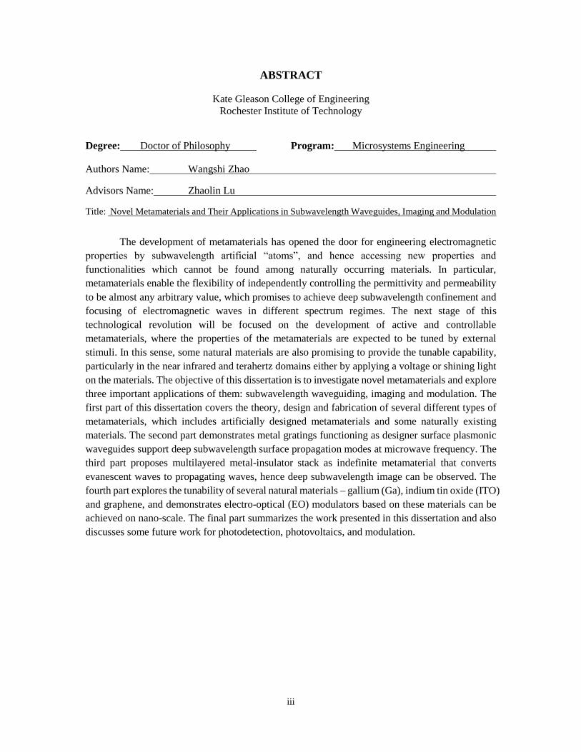
ABSTRACT
Kate Gleason College of Engineering
Rochester Institute of Technology
Degree: Doctor of Philosophy Program: Microsystems Engineering
Authors Name: Wangshi Zhao
Advisors Name: Zhaolin Lu
Title: Novel Metamaterials and Their Applications in Subwavelength Waveguides, Imaging and Modulation
The development of metamaterials has opened the door for engineering electromagnetic
properties by subwavelength artificial “atoms”, and hence accessing new properties and
functionalities which cannot be found among naturally occurring materials. In particular,
metamaterials enable the flexibility of independently controlling the permittivity and permeability
to be almost any arbitrary value, which promises to achieve deep subwavelength confinement and
focusing of electromagnetic waves in different spectrum regimes. The next stage of this
technological revolution will be focused on the development of active and controllable
metamaterials, where the properties of the metamaterials are expected to be tuned by external
stimuli. In this sense, some natural materials are also promising to provide the tunable capability,
particularly in the near infrared and terahertz domains either by applying a voltage or shining light
on the materials. The objective of this dissertation is to investigate novel metamaterials and explore
three important applications of them: subwavelength waveguiding, imaging and modulation. The
first part of this dissertation covers the theory, design and fabrication of several different types of
metamaterials, which includes artificially designed metamaterials and some naturally existing
materials. The second part demonstrates metal gratings functioning as designer surface plasmonic
waveguides support deep subwavelength surface propagation modes at microwave frequency. The
third part proposes multilayered metal-insulator stack as indefinite metamaterial that converts
evanescent waves to propagating waves, hence deep subwavelength image can be observed. The
fourth part explores the tunability of several natural materials – gallium (Ga), indium tin oxide (ITO)
and graphene, and demonstrates electro-optical (EO) modulators based on these materials can be
achieved on nano-scale. The final part summarizes the work presented in this dissertation and also
discusses some future work for photodetection, photovoltaics, and modulation.

iv
ACKNOWLDEDGMENTS
I felt so fortunate to be surrounded by many loving people and now it is my pleasure
to thank all of them for their love, encouragement, support and blessings.
First of all, I would like to express my sincerest gratitude to my advisor Professor
Zhaolin Lu, for his valuable guidance and generous support throughout my entire graduate
studies at RIT. His pioneering vision in optical science, abundance of knowledge and hard-
working spirit inspired and motivated me. Without his insightful suggestions and persistent
help, this dissertation would not have been possible.
I would like to express my deepest appreciation to Professor Bruce W. Smith,
Professor Jayanti Venkataraman, Professor Stefan F. Preble, and Professor Behnaz
Ghoraani for serving as my dissertation committee, willing to share their invaluable
opinions and their useful critiques on my research.
I would like to thank the staff members in the Semiconductor & Microsystems
Fabrication Laboratory (SMFL), especially Mr. Sean O’Brien and Mr. Bruce Tolleson.
Their willingness to give their time and help so generous have been appreciated. At the
same time, I would like to thank the staff members at Cornell NanoScale Science &
Technology Facility (CNF), especially Mr. Aaron Windsor. For his expertise and
instruction to me. My grateful thanks are also extended to Professor Karl Hirschman and
Ms. Patrica Meller, for their kindness and help to me.
I want to express my gratitude to Dr. Ruoxi Yang, Dr. Rami Wahsheh, Mr. Andrew
Estroff and Mr. Liang Cao, for their help in offering me useful technical discussions.
Special thanks should be given to Ms. Fan Yang and Mr. Chih-Yu Jen. As my best friends,
they gave me encouragement all the time and accompanied me during my ups and downs.
Finally, I would like to express my appreciation to my dearest parents, Mr. Zongpei
Zhao and Ms. Shuwen Liu. Thanks for their unconditional love to me, trust me and always
being on my side.
v
TABLE OF CONTENTS
1 Introduction ................................................................................................................. 1
1.1 Motivation ........................................................................................................... 1
1.2 Metamaterials ...................................................................................................... 3
1.2.1 Background ..................................................................................................... 3
1.2.2 Negative refraction and subwavelength imaging ............................................ 5
1.2.3 Indefinite metamaterial ................................................................................... 8
1.2.4 Designer surface plasmonic metamaterials ................................................... 11
1.2.5 Graphene ....................................................................................................... 14
1.2.6 Transparent conductive oxides (TCOs) ........................................................ 18
1.3 Fabrication of Metamaterial Samples ............................................................... 21
1.3.1 Metamaterial with artificially designed structures ........................................ 21
1.3.2 Graphene synthesis, transfer and characterization ........................................ 22
1.3.3 ITO deposition and annealing ....................................................................... 27
1.4 Finite-Difference Time-Domain (FDTD) Modeling ........................................ 28
1.5 Dissertation Overview ...................................................................................... 30
1.6 Contributions ..................................................................................................... 32
2 Deep Subwavelength Waveguiding and Focusing based on Designer Surface
Plasmons ........................................................................................................................... 34
2.1 Introduction ....................................................................................................... 34
2.2 Design and Fabrication ..................................................................................... 35
2.2.1 Modeling ....................................................................................................... 35
2.2.2 Fabrication and experimental setup .............................................................. 37
2.3 Experimental results and analysis ..................................................................... 38
2.3.1 3D DSP waveguide ....................................................................................... 38
vi
2.3.2 3D directional coupler ................................................................................... 41
2.3.3 Tapered 3D DSP waveguide ......................................................................... 42
2.4 Conclusions ....................................................................................................... 43
3 Super Talbot Effect in Indefinite Anisotropic Metamaterial .................................... 44
3.1 Introduction ....................................................................................................... 44
3.1.1 TE and TM waves ......................................................................................... 44
3.1.2 Classical Talbot effect ................................................................................... 49
3.1.3 Talbot effect in plasmons .............................................................................. 51
3.2 Design and Modeling ........................................................................................ 53
3.2.1 Structure design ............................................................................................ 53
3.2.2 Talbot distance in indefinite metamaterial .................................................... 54
3.3 Results and Discussion ..................................................................................... 55
3.3.1 Talbot effect without paraxial approximation ............................................... 55
3.3.2 Classical Talbot effect in indefinite metamaterial ........................................ 56
3.3.3 Super Talbot effect in indefinite metamaterial ............................................. 57
3.3.4 Super Talbot effect demonstrated in 3D simulations .................................... 58
3.4 Conclusions ....................................................................................................... 60
4 Nanoplasmonic Optical Switch Based on Ga-Si3N4-Ga Waveguide ........................ 62
4.1 Introduction ....................................................................................................... 62
4.2 Design and Modeling ........................................................................................ 65
4.2.1 2D FDTD simulation results ......................................................................... 67
4.2.2 3D FDTD simulation results ......................................................................... 71
4.3 Proposed Fabrication Steps ............................................................................... 72
4.4 Conclusions ....................................................................................................... 73
5 ITO-Based Multilayer Electro-Optical Modulator ................................................... 75

vii
5.1 Introduction ....................................................................................................... 75
5.2 Transfer Matrix Method (TMM) ...................................................................... 77
5.2.1 Single boundary ............................................................................................ 77
5.2.2 Propagation in a multilayer stack .................................................................. 78
5.3 Drude model ...................................................................................................... 79
5.4 Optical property of ITO .................................................................................... 82
5.5 ITO-based multilayer modulators ..................................................................... 84
5.5.1 Fabrication of multilayer structure ................................................................ 84
5.5.2 Experimental demonstration of modulation effect ....................................... 85
5.5.3 Preliminary result for real-time response ...................................................... 89
5.6 Conclusions ....................................................................................................... 90
6 Ultracompact Electro-Optic Modulators based on ENZ-Slot Waveguide ................ 91
6.1 Introduction ....................................................................................................... 91
6.2 Tunable ENZ-slot waveguides .......................................................................... 93
6.2.1 Epsilon-near-zero (ENZ) state ...................................................................... 93
6.2.2 Significantly enhanced absorption by ENZ state .......................................... 94
6.3 Nanoscale EO modulators ................................................................................. 96
6.3.1 Mode profiles ................................................................................................ 96
6.3.2 Performance Analysis ................................................................................... 97
6.4 Conclusions ....................................................................................................... 99
7 Greatly Enhanced Absorption of Monolayer Graphene in An Ultrabroad Band .... 101
7.1 Introduction ..................................................................................................... 101
7.2 Optical Absorption of Graphene and Its Applications .................................... 102
7.3 Enhanced Optical Absorption by Graphene ................................................... 104
7.3.1 Background ................................................................................................. 104

viii
7.3.2 Numerical Analysis ..................................................................................... 105
7.3.3 Experimental Results and Discussion ......................................................... 108
7.4 Conclusions ..................................................................................................... 114
8 Nanoscale Electro-Optic Modulators Based on Graphene ..................................... 115
8.1 Introduction ..................................................................................................... 115
8.2 Intraband absorption of graphene ................................................................... 116
8.2.1 Surface conductivity model of graphene .................................................... 116
8.2.2 Intraband absorption ................................................................................... 117
8.3 Design and modeling ...................................................................................... 119
8.3.1 Significantly enhanced absorption in graphene-slot waveguide ................. 119
8.3.2 Mode profiles .............................................................................................. 121
8.4 Performance analysis ...................................................................................... 123
8.4.1 Insertion loss ............................................................................................... 123
8.4.2 Bandwidth ................................................................................................... 124
8.4.3 Power consumption, modulation speed and thermal effect ........................ 126
8.5 Conclusions ..................................................................................................... 128
9 Conclusions ............................................................................................................. 129
9.1 Designer surface plasmonics (DSP) and indefinite metamaterials ................. 129
9.2 Tunable metamaterials .................................................................................... 130
9.3 Future work ..................................................................................................... 131
10 Publications ............................................................................................................. 133
10.A Peer reviewed journals: ................................................................................... 133
10.B Conferences: ................................................................................................... 133
11 References ............................................................................................................... 135

ix
LIST OF FIGURES
Figure 1.1 A three-dimensional metamaterial and its unit cell, where the unit cell is
arranged in a body-centered-cubic structure. [9] ·································· 1
Figure 1.2 Material parameter space. [11,12,15] ················································· 4
Figure 1.3 (a) Evanescent waves can be enhanced by a negative refractive index
metamaterial, so the amplitudes of the evanescent waves are identical at the
object and the image plane. (b) Propagating waves in the metamaterial. [27] 6
Figure 1.4 Superlens at microwave frequencies with a loaded transmission-line structure
[6] (a-b). (a) The planar transmission-line lens. (b) The measured electric field
at source (dashed curve), image (solid curve), and diffraction limit (dash-dotted
curve with triangles). Superlens at mid-infrared frequencies with an 880nm-
thick SiO2-SiC-SiO2 structure [7] (c-g). (c) Experimental setup. (d) Scanning
electron micrograph of the object plane, showing the holes in the Au film. (e)
Infrared amplitude in the image plane at λ=10.85µm. (f) Infrared phase contrast
at λ=11.03µm. (g) Control image of amplitude at λ=9.25µm. Superlens at
optical frequencies with a thin Ag film [5] (h-k). (h) Experimental setup. (i)
Focused ion beam (FIB) image of the object. (j) Atomic force microscopy
(AFM) image of the developed image on photoresist with a silver superlens.
(k) Control image on the photoresist when the silver was replaced by PMMA.
···························································································· 7
Figure 1.5 (a) A sample of indefinite metamaterial with the coordinates, in which εi(εm) and
di(dm) are the permittivity and the thickness of dielectric material(metal),
respectively. (b) The permittivity of a metamaterial constructed by Ag and
x
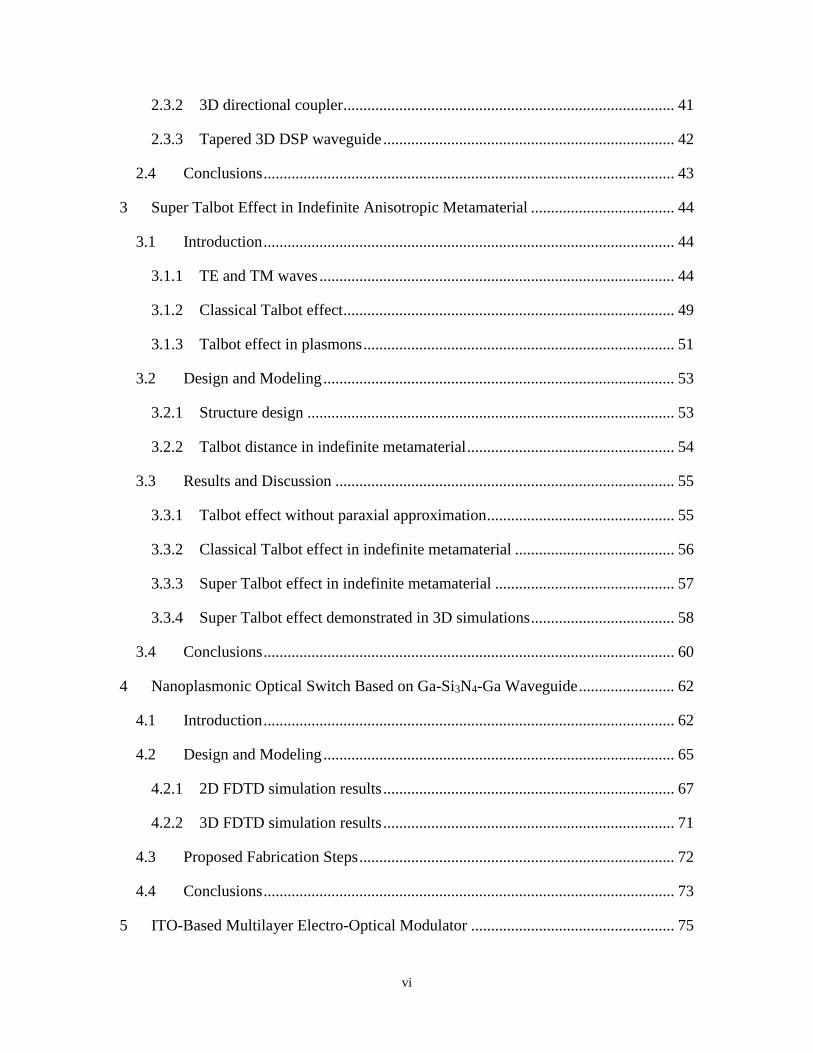
SiO2, at λ=630nm, with a varying thickness ratio η. (c) The permittivity of the
metamaterial with a fixed thickness ratio η=1.5, at varying thickness. The real
of εz and εx have opposite signs in the yellow shadowed areas in both figures.
·························································································· 10
Figure 1.6 The transmitted electric field intensity for a line source, imaged by a
metamaterial slab of thickness 1/k0. The material parameters used correspond
to layers of Ag and ZnS-SiO2, embedded in crystalline Ge2Sb2Te5 (a phase-
change material used in optical storage devices), for light of wavelength 650nm.
The corresponding total slab width is around 105nm. [35] ···················· 11
Figure 1.7 (a) A one-dimensional array of grooves of width a, depth h, and periodicity d.
[53] (b) An a × a square holes arranged on a d × d lattice are cut into the surface
of a perfect conductor, in which localized surface plasmon modes can be
induced by the structure. [54] (c) The dispersion relation [ω(kx)] of the surface
bound states supported by the one-dimensional array of grooves [Fig. 1.7(a)],
with geometrical parameters a/d=0.2 and h/d=1. [53] ·························· 13
Figure 1.8 (a) Field concentration via adiabatically increased groove depth. Distribution of
the E field, evaluated at f=0.6 THz, along the radial direction at different
locations of the wire corresponding to different depth. The inset shows the
distribution of the E field on a logarithmic scale. [59] (b) Superfocusing on a
corrugated cone of length 2mm (shown in the magnitude of E field on a
logarithmic scale), with constant groove depth 5µm and groove period 50µm.
The radius of the cone is reduced from 100 to 10µm. [59] (c) Dispersion
relation of designer surface plasmon waveguides for various lateral widths L.

xi
Inset: diagram of the structure and geometric parameters. [63] (d) Left:
Poynting vector field distribution in a horizontal plane of the tapered
waveguide. Right: Amplitude of electric field in transverse vertical planes at
locations shown by white dashed lines in left. [63] ····························· 14
Figure 1.9 Simulation results showing: (a) TM SPP wave pattern on graphene with two
different voltage bias; (b) graphene waveguide; and (c) graphene beam splitter.
The launched TM SPP is with a frequency f=30THz. [77] ····················· 16
Figure 1.10 (a) Illustration of the plasmon modulator. A gate bias is applied to the graphene
monolayer by applying a voltage from the Au contacts to the doped Si substrate.
(b) Low-loss state. (c) High-loss state. [78] ······································ 17
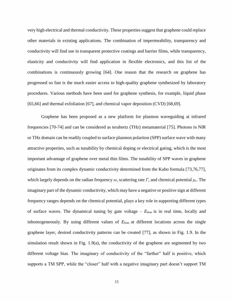
Figure 1.11 (a) Graphene-based electro-optical modulator, where a monolayer graphene is
put on top of a silicon waveguide. (b) Static electro-optical response of the
modulator at different drive voltages. [79] ······································· 18
Figure 1.12 (a) SPP penetration depth ld to an adjacent dielectric medium (air) for silver
(1), gold (2), ITO (3), ZITO [ZnO0.05:SnO20.05:In2O30.9, by weight] (4),
and AZO (5). Grey solid line is for ld =λ/2. Experimental spectral of real (b)
and imaginary (c) part of permittivity for ITO (1), ZITO (2), AZO (3), and
ITZO (4). [23]········································································· 19
Figure 1.13 (a) Structure schematics. When a voltage is applied to the MOS device, an
accumulation layer forms. (b) The carrier density are modified by an applied
voltage across the insulator/active material interface. (c) Refractive index
modulation. Dashed red/solid green: with/without charge accumulation. [24]
·························································································· 20

xii
Figure 1.14 (a) Microwave invisible cloaks [87]. (b) Terahertz metamaterial [88]. (c) and
(d) Optical metamaterials. [84] ····················································· 22
Figure 1.15 Several methods of mass-production of graphene, which allow a wide choice
in terms of size, quality and price for any specific application. [64] ········· 23
Figure 1.16 (a) Process for transferring as-grown graphene to a desired target. (b) PMMA-
supported graphene on the target. (c) After oxygen etching, the graphene region
is highlighted by the yellow dashed lines. ········································ 25
Figure 1.17 (a) Raman spectrum of highly ordered pyrolytic graphite (HOPG). (b)
Illustration of as layer increases, the G-band shifts. [101] ····················· 26
Figure 1.18 The significant different band shapes (red curves) of 2D-band with the number
of layers on each. [102] ······························································ 27
Figure 1.19 Real (a) and imaginary (b) parts of permittivity of ITO annealed at various
conditions (N2, 450°C; N2, 650°C; O2, 450°C; O2, 650°C). [107] ············ 28
Figure 1.20 Yee’s spatial grid. (Internet) ························································ 30
Figure 2.1 (a) 3D DSP waveguide. (b) Two identical 3D waveguides are aligned and
forming a directional coupler. (c) Tapered DSP waveguide with a 2D
waveguide as input. [85] ···························································· 37
Figure 2.2 Experimental setup based on VNA and XYZ stages. ···························· 38
Figure 2.3 The dispersion diagram of DSP waveguides. The parameters of the waveguides
are d = 12.7mm, a = 6.35mm, and h = 19.05mm. The width of the 2D DSP
waveguide is assumed to be infinite; the width of the 3D DSP waveguide is w

xiii
= 6.35mm. The circles indicate the measured dispersion relation for the 3D
DSP waveguide. [85] ································································ 40
Figure 2.4 (a) The fabricated 3D DSP waveguide. The measured mode profiles (shown in
normalized intensity) in different directions: (b) Side (over rods, in x-z plane),
(c) Cross section over a rod (in y-z plane), (d) Top view (over rods, in x-y plane),
the dashed blue squares indicate the positions of the metal rods, (e) Cross
section in a groove (in y-z plane), (f) Cross section along the side wall of a rod
(in y-z plane). [85] ···································································· 41
Figure 2.5 (a) Two DSP waveguides in parallel form a directional coupler. (b) The EM
wave (shown in normalized amplitude) propagates in the directional coupler.
[85] ····················································································· 41
Figure 2.6 (a) The integration of the 3D subwavelength DSP waveguide with a tapered
DSP waveguide as input. (b) Experimental result of normalized intensity
distribution when EM waves are coupled from a 2D DSP waveguide and a 3D
DSP waveguide. [85] ································································ 42
Figure 3.1 Illustration of oblique incidence for (a) TM- and (b) TE-polarized light. ····· 45
Figure 3.2 (a) Illustration of a SPPs as a collective excitation at a metal-dielectric interface.
The electric field E and magnetic field H are enhanced at the interface. (b) The
perpendicular field Ez decays exponentially with a characteristic length δd in
the dielectric and δm in metal. [122] ··············································· 46
Figure 3.3 Illustration of the optical Talbot effect, shown as a Talbot carpet. [130]······ 50
xiv
Figure 3.4 (a) Illustration of the plasmon Talbot effect above a metal surface. Numerically
computed plasmon Talbot carpets for a metal film drilled by an array of
nanoholes with different periods a: (b) a=λsp, (c) a=5λsp, (d) and (e) a=20λsp.
[141] ···················································································· 52
Figure 3.5 (a) Left: Illustration of the SPPLGs. Right: scanning electron micrograph of the
SPPLG with d=6λsp and α=1/2. Experimental Talbot carpets for the SPPLGs
with d=3λsp (b) and d=6λsp (c), respectively. [142] ······························ 53
Figure 3.6 Schematic illustration of the investigated structure, the 1D grating is assumed
to be infinite along y-axis. [121] ··················································· 54
Figure 3.7 Without paraxial approximation: (a) No Talbot effect is seen in air. (b) Periodic
Talbot carpet pattern can be observed in indefinite metamaterial (shown in
normalized H field distribution). [121] ············································ 56
Figure 3.8 Talbot effect in (a) air, and (b) indefinite metamaterial. Both are shown in
normalized power distribution. [121]·············································· 57
Figure 3.9 (a) Super Talbot effect in an Ag-SiO2 stack (shown in normalized power). (b)
Cross-sectional power profile along the white solid line shown in (a), where x
= 52nm. [121] ········································································· 58
Figure 3.10 (a) Illustration of the structure. Hole diameter: 2r = 80nm, hole array periods:
D = 150nm along x and y axes. Incident wavelength is λ0 = 630nm. (b) The
Talbot carpet pattern in the vertical z-y plane at x = 0. (c) Talbot carpet pattern
in the horizontal z-x plane at y = 0. (d) One integer Talbot imaging plane. (e)

xv
One fractional Talbot imaging plane with z =2/3ZT. (b-e) are shown in
normalized |E|2. [121] ································································ 59
Figure 4.1 Surface light-induced metallization at a gallium-silica interface, at a wavelength
of 1.55μm. [149] ······································································ 64
Figure 4.2 A SPP-based gold-on-quartz waveguide containing a gallium switching section,
where gallium is at the bottom of the quartz substrate, shown in the magnitude
of the magnetic field. [154] ························································· 65
Figure 4.3 (a) A Ga-Si3N4-Ga plasmonic waveguide embedded between two silicon
dielectric waveguides. (b) Dielectric gaps are introduced at both ends of the
plasmonic waveguide. [150] ························································ 66
Figure 4.4 (a) Simulation result of field distribution with metallic gallium. (b) Simulation
result of field distribution with α-gallium, CB [150]. Both plots are normalized
with the result with metallic gallium. ············································· 68
Figure 4.5 Power transmission of the Ga-Si3N4-Ga plasmonic waveguide as a function of
wavelength for different phases and crystalline directions of gallium. [150] 69
Figure 4.6 (a) Power transmission as a function of the depth d of metallic gallium thin film.
(b) Extinction ratios of the Ga-Si3N4-Ga plasmonic waveguide as a function of
d. [150] ················································································· 71
Figure 4.7 (a) Starting the fabrication process on an SOI wafer. (b) Defining the input and
output silicon waveguide. (c) Deposition of Si3N4 film as the core of the
plasmonic waveguide. (d) Deposition of gallium film. [150] ·················· 72

xvi
Figure 4.8 Extinction ratio as a function of thickness of silicon nitride or gallium film. [150]
·························································································· 73
Figure 5.1 Oblique incidence. ····································································· 78
Figure 5.2 Illustration of a planar multilayer stack, incoming light comes from medium 0
and leaves the stack from medium (i-1). ·········································· 78
Figure 5.3 ATR setup in Kretschmann configuration.········································· 82
Figure 5.4 (a) Fitted permittivity of an ITO on glass sample. (b) Measured reflectance
curves. ·················································································· 83
Figure 5.5 Illustration of ITO-based multilayer modulator: (a) ITO/gel/doped-Si, and (b)
ITO/gel/ITO. (c) Commercial Electrolyte gel. ··································· 84
Figure 5.6 Normalized reflectance as a function of angle for the ITO/electrolyte
gel/heavily-doped Si modulator with different applied voltages. Inset:
illustration of the modulator with applied voltage. ······························ 86
Figure 5.8 Normalized reflectance as a function of angle for the ITO/electrolyte gel/ITO
modulator with different applied voltages. Inset: illustration of the modulator
with applied voltage. ································································· 88
Figure 5.9 Ionic relaxation effect of the electrolyte gel, at an angle of θ = 65°. ··········· 90
Figure 6.1 (a) Real part and imaginary part of the dielectric constant of ITO as a function
of wavelength at two different carrier concentration based on Drude model. (b)
The illustration of ENZ-slot waveguides.········································· 94
Figure 6.2 (a) The plots of the transverse electric field magnitude across the ENZ-slot MIM
plasmonic waveguide at N=N1 and N=N2, respectively. (b) The plots of the

xvii
transverse electric field magnitude across the ENZ-slot dielectric waveguide at
N=N1 and N=N2, respectively. ······················································ 96
Figure 6.3 The electric field profiles, effective indices, and propagation loss for different
ITO-slot waveguides at N=N1 and N=N2, respectively: (a) in a plasmonic
waveguide; (b) in dielectric rib waveguide. The refractive indices of the
semiconductor and SiO2 are assumed to be 3.45 and 1.45, respectively. All
mode profiles are shown in normalized electric fields. ························· 97
Figure 6.4 (a) The illustration of an EO modulator embedded in a plasmonic rib waveguide.
(b,c) The 3D simulation of light propagation between a plasmonic rib
waveguide and the EO modulator at N=N1 and N=N2, respectively. (d) The
illustration of an EO modulator embedded in a dielectric rib waveguide. (e, f)
The 3D simulation of light propagation between a dielectric rig waveguide and
the EO modulator at N=N1 and N=N2, respectively. (b), (c), (e) and (f) are
shown in normalized power distribution. ········································· 99
Figure 7.1 Illustration of the graphene (upper), 0D bucky balls (lower left), 1D nanotubes
(lower middle), and 3D graphite (lower right). [231] ·························· 102
Figure 7.2 (a) Numerical calculation of the reflectance and absorption as functions of
incident angle, θ1, and substrate refractive index n3. (b) Calculation of
maximum achievable absorption as a function of substrate refractive index n3.
Results in (a) and (b) are obtained at λ=650nm for s-polarized light, and
n1=1.51. [205] ········································································ 105

xviii
Figure 7.3 Illustration of the experimental setup for ATR measurement. The red dashed
line represents the monolayer graphene film. P1 and BS represent the polarizer
and beam splitter, respectively. [205] ············································ 108
Figure 7.4 Raman spectroscopy result for the graphene sample. The three curves represent
three different points on the same sample. [274] ······························· 109
Figure 7.5 Reflectance of a reference BK7 glass slide (blue triangles), monolayer graphene
(red circles), and numerical fit (green) with an s-polarized light (a) with
wavelength of λ = 650 nm and (b) λ = 1520 nm. In the legend, “G” represents
“graphene”. “BK7/G/air” means the result with the BK7(prism)-graphene-air
configuration. [205] ································································· 110
Figure 7.6 (a) Normalized measured reflectance of the monolayer graphene with M1.50 as
substrate under s-polarized light incidence at λ=650nm. (b) Measured
reflectance of the monolayer graphene with M1.50 as substrate under s-
polarized light incidence at λ=1520nm. In both graphs, red curves represent the
results when a BK7 deflector is used; blue curves represent the results when a
BSG deflector is used. In the legend, “G” and “M” represent “graphene” and
“matching liquid”, respectively. “BK7/G/M/BK7” means the result for the
BK7(prism)-graphene-M1.50(substrate)-BK7(deflector) configuration. [205]
························································································· 111
Figure 7.7 For 1520nm p-polarized light incidence, the normalized measured reflectance
by the monolayer graphene sample as a function of incident angle when (a) the
substrate is air, and (b) the substrate is M1.50. [205] ·························· 113

xix
Figure 8.1 (a) Real part and (b) imaginary part of the graphene conductivity as a function
of chemical potential and wavelength (T = 300K) based on the Kubo formula.
(c) The graphene conductivity (real part and imaginary part), by interband
transition and intraband transition, as the function of chemical potential at λ0 =
1550nm. (d) The effective dielectric constant (real part, imaginary part, and
magnitude) as a function of chemical potential at λ0 = 1550nm. (e) The
illustration of a 2D “graphene-slot waveguide” with a 10nm thick Si3N4 buffer
layer on each side of graphene. (f) The plots of the transverse electric field
magnitude across the waveguide at μc = 0 and μc = μt, respectively. [222] · 119
Figure 8.2 Mode profiles for graphene on top of dielectric waveguide. [247] (a) At μc = 0,
attenuation α= 0.134dB/μm, and (b) at μc = 0.515 eV, attenuation α=
0.044dB/μm. Both figures are shown in normalized electric fields. ········· 120
Figure 8.3 The transverse electric field profiles, effective indices, and propagation loss for
different graphene-slot waveguides at μc = 0 and μc = μt, respectively: (a) in a
dielectric waveguide (Si waveguide is 450nm wide and 150nm thick for each
layer); (b) in a dielectric strip waveguide (strip Si waveguide is 450nm wide
and 150 nm thick for each layer); (c) in a metal-insulator-metal waveguide
(waveguide is 200 nm wide); (d) in a metal strip waveguide (strip metal is
200nm wide); (e), (f) in photonic-plasmonic hybrid waveguides [waveguide is
400 nm wide in (e) and 200 nm wide in (f), Si layer is 130 nm thick for both
structures]. All mode profiles are shown in normalized electric fields. The
refractive indices of Si, Si3N4, and SiO2 are assumed to be 3.47, 1.98, and 1.44,
respectively. [222] ··································································· 122

xx
Figure 8.4 The illustration of a graphene EO modulator based on a silicon waveguide. (b),
(c) The 3D simulation of light propagation between a silicon waveguide and
the EO modulator at μc = 0 and μc = μt, respectively. (d) The illustration of a
graphene EO modulator based on a metal strip plasmonic waveguide. (e), (f)
The 3D simulation of light propagation between a metal strip plasmonic
waveguide and the EO modulator at μc = 0 and μc = μt, respectively. Figures
(b), (c), (e) and (f) are shown in normalized power distribution. [222] ····· 124
Figure 8.5 The attenuation of graphene-slot modulators as a function of working
wavelength at μc = 0 and μc = μt, respectively: (a) in a silicon waveguide; (b)
in a metal strip waveguide. The attenuation of graphene-slot waveguides as a
function of chemical potential and gate voltage at a wavelength of 1550nm; (c)
in a silicon waveguide (450nm wide and 150nm thick for each layer); (d) in a
metal strip plasmonic waveguide (strip metal is 200nm wide). [222] ······· 126
Figure 8.6 The illustration of nanoscale graphene modulators containing direct graphene-
semiconductor contacts based on (a) dielectric strip waveguide, and (b) metal
strip waveguide. [222] ······························································ 128

xxi
LIST OF TABLES
Table 6.1 Free carrier concentrations in ITO. ·················································· 93

xxii
LIST OF ACRONYMS
AFM .................... Atomic Force Microscopy
ATR ..................... Attenuated Total Reflection
AZO ................... Aluminum-doped Zinc Oxide
CVD .................... Chemical Vapor Deposition
DSP ..................... Designer Surface Plasmon
DUV .................... Deep Ultraviolet
EA ....................... Electro-Absorption
EM ....................... Electromagnetic
EMT .................... Effective Medium Theory
ENZ ..................... Epsilon-Near-Zero
EO ....................... Electro-Optic
FDTD .................. Finite-Difference Time-Domain
FWHM ................ Full Width at Half Maximum
ITO ...................... Indium Tin Oxide
MMI .................... Multilayer Metal-Insulator
NIMs ................... Negative Index Metamaterials
NIR ...................... Near-Infrared
PEC ..................... Perfect Electric Conductor
PECVD ............... Plasma-Enhanced Chemical Vapor Deposition
SPPs .................... Surface Plasmon Polaritons

xxiii
SRRs ................... Split Ring Resonators
TCOs ................... Transparent Conductive Oxides
TE ........................ Transverse Electric
TM ....................... Transverse Magnetic
TMM ................... Transfer-Matrix Method
VNA .................... Vector Network Analyzer
1 INTRODUCTION
1.1 Motivation
Electromagnetic (EM) metamaterials, with their extraordinary properties which cannot be
obtained in most naturally existing materials, have been shown tremendous potentials in many
fields of science and technology. Many scientific breakthroughs, for example, invisible cloaking
[1-3] and super lenses [4-7], have been experimentally demonstrated with metamaterials.
Generally, metamaterials can be treated as effective media, where their extraordinary properties
depend on their periodic structure rather than their composition [8]. The periodicity of each unit
cell in a metamaterial is significantly smaller than the wavelength of interest. Therefore, each unit
can be viewed as a microscopic building block of the metamaterial, in analogy to the atoms in the
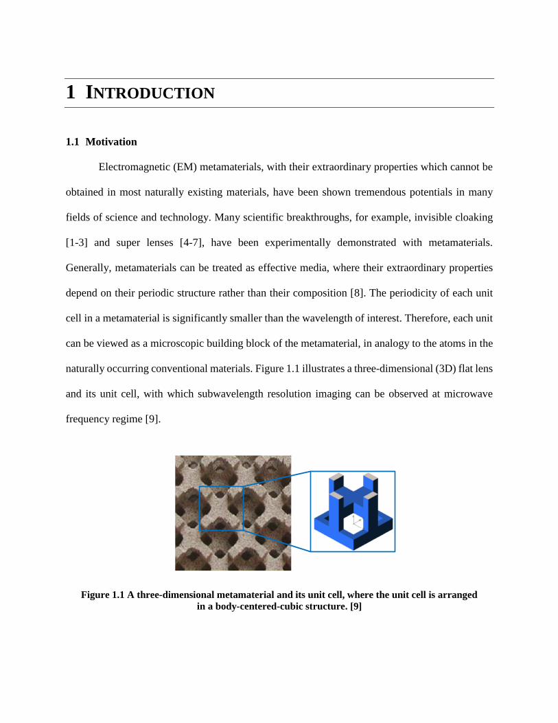
naturally occurring conventional materials. Figure 1.1 illustrates a three-dimensional (3D) flat lens
and its unit cell, with which subwavelength resolution imaging can be observed at microwave
frequency regime [9].
Figure 1.1 A three-dimensional metamaterial and its unit cell, where the unit cell is arranged
in a body-centered-cubic structure. [9]

2
The history of metamaterials dates back to 1968, when a Russian scientist, Veselago,
theoretically investigated [10] the electromagnetic consequences of a material which has both
negative ε and negative µ, and made a conclusion that the refractive index of the material should
be revised and expressed as . Materials with negative refractive index n have numerous
interesting applications and many classical physical phenomena associated with EM wave
propagation need to be reexamined. For example, Doppler shift is reversed, and Cherenkov
radiation is emitted in the opposite direction to the charge’s motion rather than in the forward
direction [10]. However, Veselago’s theoretical work on the negative refractive index material had
not been experimentally demonstrated for a long time since materials with negative index do not
exist in nature. In 1990s, John B. Pendry and his colleagues proposed, for the first time, to use
artificial materials to realize negative permittivity [11] and negative permeability [12], which
opened up a completely new research area -- metamaterials.
At the early stage, the research on metamaterials was focused on microwave region to
demonstrate negative refractive index [13] and superlenses [14]. In recent years, most efforts were
focused on the engineering and extension of the functionalities of metamaterials at terahertz [16-
18] and optical [5,13,19,20] frequencies. More recently, researchers focus on the metamaterial
design which leads to the realization of tunability in metamaterials [19,21,22]. Tunable
metamaterials are designed for switching and modulating EM waves if the properties of the
metamaterials can be controlled by applying external stimulus. Some natural materials, such as
graphene and transparent conductive oxides (TCOs), have already shown their outstanding
properties as tunable metamaterials [23-25]. In this dissertation, I have explored the field of novel
metamaterials and addressed three important applications of metamaterials: subwavelength
waveguiding, imaging and modulating. These applications have been explored in an integrated

3
approach: starting from a fundamental study of subwavelength waveguiding with a designer
surface plasmon (DSP) waveguide at microwave frequency regime, then extending the exploration
to imaging beyond diffraction limit and modulating at optical frequencies.
1.2 Metamaterials
From a theoretical concept proposed several decades ago, the research on the topic of
metamaterials is now rapidly expanding. With the fast development of nano-fabrication techniques,
metamaterial are not limited to the microwave region, more complex structures working at higher
frequencies can be fabricated and a wider range of materials can be selected. In this section, several
different types of metamaterial designs, as well as their properties and applications will be
introduced.
1.2.1 Background
Materials play key roles in the development of optics and photonics, since the main
objective in these fields is to obtain the control on light propagation and light-matter interaction.
In a conventional material, the propagation of light is influenced by the local refractive index
. The EM response of a metamaterial can be described with two frequency-dependent
macroscopic parameters, permittivity ε(ω) and permeability µ(ω). Figure 1.2 shows a “material
parameter space”, which includes all types of materials, as far as EM properties are concerned.
Region I represents materials with both permittivity and permeability positive, which covers most
conventional dielectric materials. Region II includes metals and heavily doped semiconductors,
which exhibit negative permittivity at some frequency regimes. In the microwave spectrum regime,
negative permittivity can also be achieved by artificially designed wire structures [11] as illustrated
in the top left. The first man-made material with negative permeability is the split ring resonators
(SRRs) [12], as shown in the top right of region IV. Region III is the most interesting one, in which

4
permittivity and permeability are simultaneously negative. No such material can be found in nature.
The representative negative index metamaterial (NIM) at microwave frequency is constructed by
the SRRs and metallic wires [15]. On the subwavelength scale, the electric and magnetic fields are
decoupled, so the permittivity ε(ω) could be the only parameter to be considered to fulfill the
requirements of the metamaterials with desired EM properties, while disregarding the permeability
µ(ω). In this dissertation, the focus will be put on the manipulation of the frequency-dependent
permittivity ε(ω), and the related novel metamaterial designs as well as their properties and
applications.
Figure 1.2 Material parameter space. [11,12,15]
One of the greatest potentials of metamaterials is the possibility to create negative
refractive index, and the associated application is super lenses with imaging resolution beyond the
diffraction limit [4]. Besides the negative refractive index, advanced developments in
metamaterials [11,12,14,15,26] promise unprecedented flexibility in providing the artificial

5
materials with very complex specifications, including independent control of the permittivity and
permeability with positive, negative, or near zero values, and with desired anisotropy and designed
gradients. Tunable metamaterials attract more attention in recent years since they show variable
response to an incident light beam, hence they are promising candidates to achieve nanometer-
scale modulators on chip. The tunability of metamaterials has been demonstrated with different
approaches, for example, electrically or optically pumping the semiconductor constituent of the
metamaterials [21,22], and external DC magnetic field tuning [19].
One of the significant challenges researchers have to face is the high loss in the
metamaterials at telecommunication and optical frequencies, which is usually caused by the metals,
metal alloys or heavily doped semiconductors in those metamaterials. These large losses seriously
limit the practicality of metamaterials for many novel applications, which is also a major obstacle
in the design of efficient devices. Hence, new materials with relatively low loss are desirable. The
introduction of alternative materials, for example, graphene and transparent conductive oxides
(TCOs), can overcome the major bottleneck and improve the performance of the devices.
Graphene, the two-dimensional atomic crystal, combines its exceptionally high electronic and
thermal conductivities, as well as many other supreme properties, all of which make it highly
attractive for numerous applications. The carrier concentration in TCOs is in the range of
1020~1021/cm3, which will shift the plasma frequency into the near infrared (NIR) regime for
telecom applications.
1.2.2 Negative refraction and subwavelength imaging
The original interest in metamaterials was triggered by Pendry’s work in 2000 [4], where
he claimed “negative refraction makes perfect imaging”. In a conventional medium, the maximum
resolution of an image cannot be smaller than the diffraction limit, because the evanescent waves

6
which carry the subwavelength feature information decay exponentially in that medium. However,
in a metamaterial with a negative refractive index, the amplitudes of the evanescent waves can be
amplified [4]. After emerging from the medium, the amplitudes will reach to the original level
[27], as shown in Fig. 1.3(a). The propagating waves pass through the NIM with both negative
refraction and a reversed phase front [as shown in Fig. 1.3(b)], which leads to zero phase change
at the image plane [27]. Therefore, both propagating and evanescent waves are recovered in phase
and amplitude, and a perfect image can be obtained.
Figure 1.3 (a) Evanescent waves can be enhanced by a negative refractive index
metamaterial, so the amplitudes of the evanescent waves are identical at the object and the
image plane. (b) Propagating waves in the metamaterial. [27]
Metamaterials with negative permittivity or permeability or both can be used as a superlens
in the form of a thin slab, which has been experimentally demonstrated at microwave [6], mid-
infrared [7], and optical frequencies [5] with different designs, as shown in Fig. 1.4. The planar
transmission-line lens, as shown in Fig. 1.4 (a), consisting of a grid of printed metallic strips loaded
with series capacitors and shunt inductors, can form a subwavelength image of 0.21 effective
wavelengths [6]. Figure 1.4 (c) illustrates the experimental setup for a near-field imaging system
with an ultra-thin SiO2-SiC-SiO2 superlens, in which 1200nm and 860nm holes can be resolved at
a mid-infrared wavelength of 11µm [7]. At optical wavelengths, the inherent resonances of a metal
(a) (b)
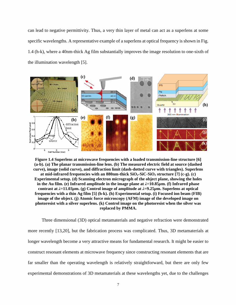
7
can lead to negative permittivity. Thus, a very thin layer of metal can act as a superlens at some
specific wavelengths. A representative example of a superlens at optical frequency is shown in Fig.
1.4 (h-k), where a 40nm-thick Ag film substantially improves the image resolution to one-sixth of
the illumination wavelength [5].
Figure 1.4 Superlens at microwave frequencies with a loaded transmission-line structure [6]
(a-b). (a) The planar transmission-line lens. (b) The measured electric field at source (dashed
curve), image (solid curve), and diffraction limit (dash-dotted curve with triangles). Superlens
at mid-infrared frequencies with an 880nm-thick SiO2-SiC-SiO2 structure [7] (c-g). (c)
Experimental setup. (d) Scanning electron micrograph of the object plane, showing the holes
in the Au film. (e) Infrared amplitude in the image plane at λ=10.85µm. (f) Infrared phase
contrast at λ=11.03µm. (g) Control image of amplitude at λ=9.25µm. Superlens at optical
frequencies with a thin Ag film [5] (h-k). (h) Experimental setup. (i) Focused ion beam (FIB)
image of the object. (j) Atomic force microscopy (AFM) image of the developed image on
photoresist with a silver superlens. (k) Control image on the photoresist when the silver was
replaced by PMMA.
Three dimensional (3D) optical metamaterials and negative refraction were demonstrated
more recently [13,20], but the fabrication process was complicated. Thus, 3D metamaterials at
longer wavelength become a very attractive means for fundamental research. It might be easier to
construct resonant elements at microwave frequency since constructing resonant elements that are
far smaller than the operating wavelength is relatively straightforward, but there are only few
experimental demonstrations of 3D metamaterials at these wavelengths yet, due to the challenges
(a)
(b)
(c) (d)
(e) (f) (g)
(h)
(i)
(j)
(k)source
diffraction
limit
image

8
faced by the fabrication of 3D periodic structures. Actually, metamaterials were initially proposed
as a 3D structure by Pendry et al in 1996 [11], as the wired structure on top left of region II shown
in Fig. 1.2. The structure dilutes the average concentration of electrons and considerably enhances
the effective electron mass through selfinductance. Therefore, such a structure can depress the
plasma frequency into the far infrared or even into the GHz band. One advantage of the structure
is that different plasma frequencies can be achieved by varying the lattice constant. Non-uniform
periods will introduce anisotropic property to the metamaterial and hence it will be a potential
candidate for the application of invisible cloaks [1-3].
1.2.3 Indefinite metamaterial
In addition to the negative index metamaterials, negative refraction and subwavelength
imaging can also occur in a simple but important metamaterial, which is constructed by a
multilayer metal-insulator stack and widely used for superlens design [28-31], optical lithography
[32], and subwavelength sensing/detecting [33].
Considering a particular anisotropic material, where the permittivity component along the
propagation direction (z-axis) is negative, i.e., 0z , and all other permittivity and permeability
components are positive (assuming a non-magnetic material, i.e., µ=1), the dispersion diagram is
in a hyperbolic form
, (1.1)
where the z axis is the light propagation direction. This kind of artificial material is named as
“indefinite metamaterial” since not all the components of permittivity and permeability has the
same sign [1].

9
The refraction behavior of an indefinite metamaterial can be determined by the rules as
below [26,34]: (1) The group velocity, specifies the direction of energy flow, which
must be normal to the equifrequency surface and in the direction where ω is increasing; (2) The
component of the group velocity which is along z-axis, vgz, must have the same sign in both media
(the air and the metamaterial), since the energy must be carried away inside the metamaterial; (3)
The wave vector kx, which is along the transverse x-axis, is continuous across the interface of the
air and the metamaterial.
Re-writing Eq. (1.1), the wave vector along the propagation direction kz can be expressed
as
(1.2)
Given and there is no cutoff for any spatial frequency kx in the metamaterial. In other
words, the indefinite metamaterial can convert the evanescent waves which would normally decay
in conventional materials into propagating waves, which enables the metamaterial functions as a
superlens to form subwavelength images [35-37].
The effective medium theory (EMT) [38] can be applied to approximate the macroscopic
behavior of the indefinite metamaterial if only thin alternating layers are included [35]. An
alternating Ag-SiO2 stack is shown in Fig. 1.5(a). The effective permittivity tensor of an indefinite
metamaterial can be determined by
(1.3)
∀
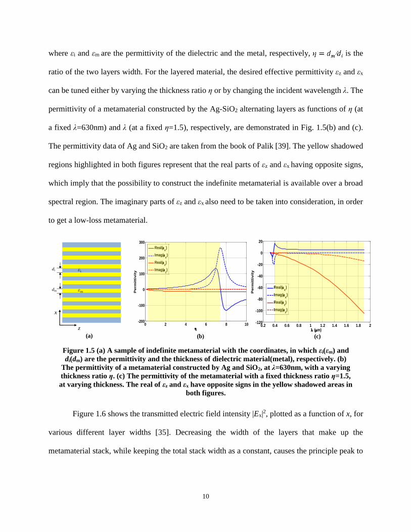
10
where εi and εm are the permittivity of the dielectric and the metal, respectively, is the
ratio of the two layers width. For the layered material, the desired effective permittivity εz and εx
can be tuned either by varying the thickness ratio η or by changing the incident wavelength λ. The
permittivity of a metamaterial constructed by the Ag-SiO2 alternating layers as functions of η (at
a fixed λ=630nm) and λ (at a fixed η=1.5), respectively, are demonstrated in Fig. 1.5(b) and (c).
The permittivity data of Ag and SiO2 are taken from the book of Palik [39]. The yellow shadowed
regions highlighted in both figures represent that the real parts of εz and εx having opposite signs,
which imply that the possibility to construct the indefinite metamaterial is available over a broad
spectral region. The imaginary parts of εz and εx also need to be taken into consideration, in order
to get a low-loss metamaterial.
Figure 1.5 (a) A sample of indefinite metamaterial with the coordinates, in which εi(εm) and
di(dm) are the permittivity and the thickness of dielectric material(metal), respectively. (b)
The permittivity of a metamaterial constructed by Ag and SiO2, at λ=630nm, with a varying
thickness ratio η. (c) The permittivity of the metamaterial with a fixed thickness ratio η=1.5,
at varying thickness. The real of εz and εx have opposite signs in the yellow shadowed areas in
both figures.
Figure 1.6 shows the transmitted electric field intensity |Ex|2, plotted as a function of x, for
various different layer widths [35]. Decreasing the width of the layers that make up the
metamaterial stack, while keeping the total stack width as a constant, causes the principle peak to
(a) (b)
0 2 4 6 8 10-200
-100
0
100
200
300
Perm
itti
vit
y
Real(x)
Imag(x)
Real(z)
Imag(z)
0.2 0.4 0.6 0.8 1 1.2 1.4 1.6 1.8 2-120
-100
-80
-60
-40
-20
0
20
(m)
Perm
itti
vit
y
Real(x)
Imag(x)
Real(z)
Imag(z)
z
x
(a) (b)
vg
εm
εi
dm
di
(a) (b) (c)

11
narrow. As the layers get thinner, the transmitted image more closely resembles the effective
medium result.
Figure 1.6 The transmitted electric field intensity for a line source, imaged by a metamaterial
slab of thickness 1/k0. The material parameters used correspond to layers of Ag and ZnS-
SiO2, embedded in crystalline Ge2Sb2Te5 (a phase-change material used in optical storage
devices), for light of wavelength 650nm. The corresponding total slab width is around 105nm.
[35]
1.2.4 Designer surface plasmonic metamaterials
Light hitting a metamaterial is transformed into electromagnetic waves of a different
variety [40], namely surface plasmon polaritons (SPPs) [41,42]. The fundamental plasma
frequency can be expressed as
(1.4)
which is proportional to the density of free carriers N, and effective electron mass m*. For metals,
the plasma frequency falls in the ultraviolet part of the light spectrum, due to the high carrier
density. The transverse mode size supported by a plasmonic waveguide is mainly determined by
the skin depth in the dielectric [43], which can be calculated as

12
(1.5)
where λ0 is the wavelength in vacuum, εd and εm are relative permittivity of the dielectric and the
metal (metal is treated as a dielectrics with complex-value permittivity), respectively. Near the
plasma frequency (in the ultraviolet regime for most metals), εm is comparable to εd, resulting in a
small transverse mode size. Recent breakthroughs have produced a wide range of nanoplasmonic
devices that generate, guide and detect light [44-51]. As the frequency decreases from the near
infrared and even down to microwave regime, most metals may be treated as perfect electric
conductors (PECs), and the penetration of the EM fields in the dielectric material extends to the
distance of the order of many wavelengths and almost completely excluded from the metal surface.
The EM waves are weakly localized at the metal-dielectric interface, and the SPPs eventually
acquire the characters of Sommerfeld or Zenneck waves [43], which are essentially grazing-
incidence light fields.
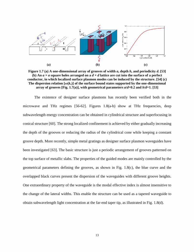
This problem can be solved by patterning a metal surface texture (e.g. periodic grooves or
holes) with subwavelength features, as shown in Fig. 1.7(a) and (b). This approach can be date
back to Goubau [43], Mills and Maradudin [52], who discovered that designed surface textures
can result in highly bounded surface waves. In those cases, the EM boundary conditions are altered
and strongly localized field radiation can be obtained at longer wavelengths. The dispersion
relation of the localized modes obtained by the one-dimensional array of grooves is shown in Fig.
1.7(c), which is similar as the one associated with the SPPs supported by the surfaces of real metals.
Therefore, this highly localized EM wave on a textured metal slab is called ‘spoof’ or ‘designer’
surface plasmons [53-55].
13
Figure 1.7 (a) A one-dimensional array of grooves of width a, depth h, and periodicity d. [53]
(b) An a × a square holes arranged on a d × d lattice are cut into the surface of a perfect
conductor, in which localized surface plasmon modes can be induced by the structure. [54] (c)
The dispersion relation [ω(kx)] of the surface bound states supported by the one-dimensional
array of grooves [Fig. 1.7(a)], with geometrical parameters a/d=0.2 and h/d=1. [53]
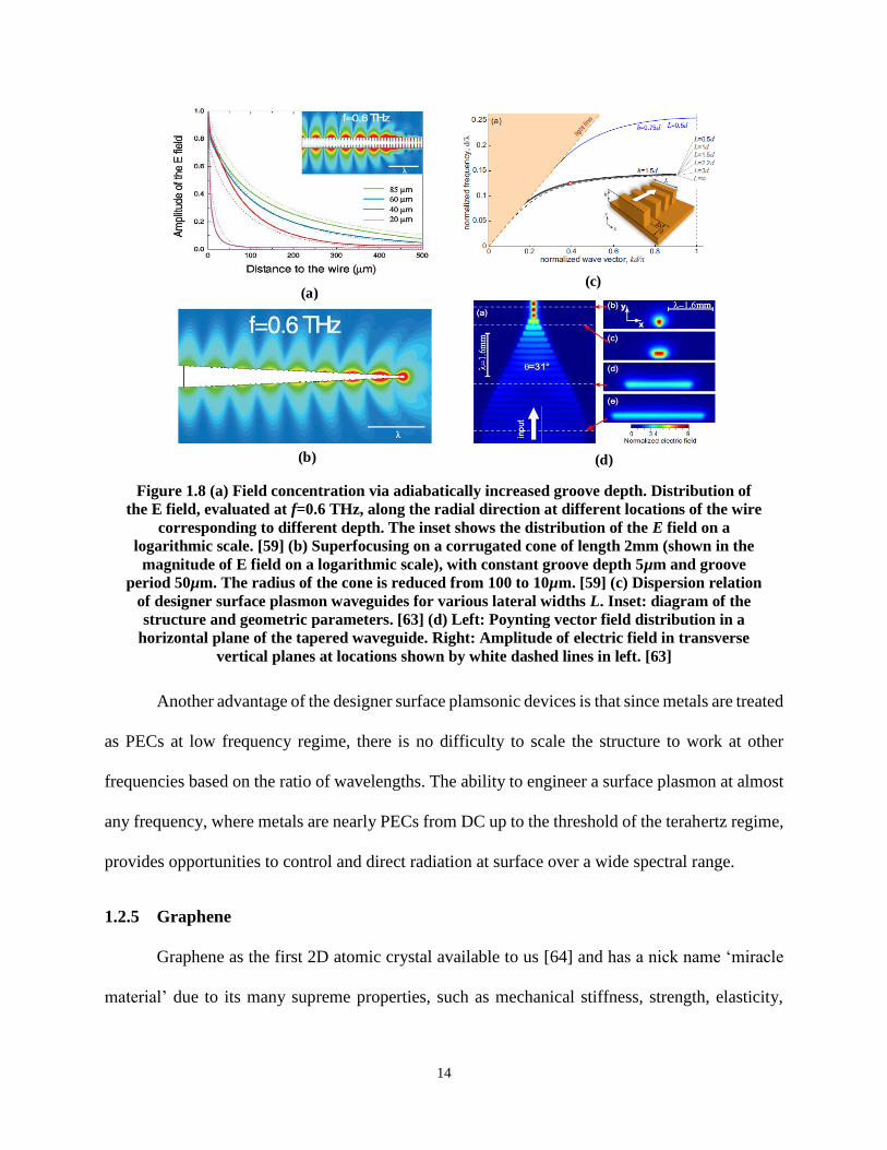
The existence of designer surface plasmons has recently been verified both in the
microwave and THz regimes [56-62]. Figures 1.8(a-b) show at THz frequencies, deep
subwavelength energy concentration can be obtained in cylindrical structure and superfocusing in
conical structure [60]. The strong localized confinement is achieved by either gradually increasing
the depth of the grooves or reducing the radius of the cylindrical cone while keeping a constant
groove depth. More recently, simple metal gratings as designer surface plasmon waveguides have
been investigated [63]. The basic structure is just a periodic arrangement of grooves patterned on
the top surface of metallic slabs. The properties of the guided modes are mainly controlled by the
geometrical parameters defining the grooves, as shown in Fig. 1.8(c), the blue curve and the
overlapped black curves present the dispersion of the waveguides with different groove heights.
One extraordinary property of the waveguide is the modal effective index is almost insensitive to
the change of the lateral widths. This enable the structure can be used as a tapered waveguide to
obtain subwavelength light concentration at the far-end taper tip, as illustrated in Fig. 1.8(d).
(a) (b) (c)
14
Figure 1.8 (a) Field concentration via adiabatically increased groove depth. Distribution of
the E field, evaluated at f=0.6 THz, along the radial direction at different locations of the wire
corresponding to different depth. The inset shows the distribution of the E field on a
logarithmic scale. [59] (b) Superfocusing on a corrugated cone of length 2mm (shown in the
magnitude of E field on a logarithmic scale), with constant groove depth 5µm and groove
period 50µm. The radius of the cone is reduced from 100 to 10µm. [59] (c) Dispersion relation
of designer surface plasmon waveguides for various lateral widths L. Inset: diagram of the
structure and geometric parameters. [63] (d) Left: Poynting vector field distribution in a
horizontal plane of the tapered waveguide. Right: Amplitude of electric field in transverse
vertical planes at locations shown by white dashed lines in left. [63]
Another advantage of the designer surface plamsonic devices is that since metals are treated
as PECs at low frequency regime, there is no difficulty to scale the structure to work at other
frequencies based on the ratio of wavelengths. The ability to engineer a surface plasmon at almost
any frequency, where metals are nearly PECs from DC up to the threshold of the terahertz regime,
provides opportunities to control and direct radiation at surface over a wide spectral range.
1.2.5 Graphene
Graphene as the first 2D atomic crystal available to us [64] and has a nick name ‘miracle
material’ due to its many supreme properties, such as mechanical stiffness, strength, elasticity,
(b) (d)
(a)(c)
15
very high electrical and thermal conductivity. These properties suggest that graphene could replace
other materials in existing applications. The combination of impermeability, transparency and
conductivity will find use in transparent protective coatings and barrier films, while transparency,
elasticity and conductivity will find application in flexible electronics, and this list of the
combinations is continuously growing [64]. One reason that the research on graphene has
progressed so fast is the much easier access to high-quality graphene synthesized by laboratory
procedures. Various methods have been used for graphene synthesis, for example, liquid phase
[65,66] and thermal exfoliation [67], and chemical vapor deposition (CVD) [68,69].
Graphene has been proposed as a new platform for plasmon waveguiding at infrared
frequencies [70-74] and can be considered as terahertz (THz) metamaterial [75]. Photons in NIR
or THz domain can be readily coupled to surface plasmon polariton (SPP) surface wave with many
attractive properties, such as tunability by chemical doping or electrical gating, which is the most
important advantage of graphene over metal thin films. The tunability of SPP waves in graphene
originates from its complex dynamic conductivity determined from the Kubo formula [73,76,77],
which largely depends on the radian frequency ω, scattering rate Γ, and chemical potential μc. The
imaginary part of the dynamic conductivity, which may have a negative or positive sign at different
frequency ranges depends on the chemical potential, plays a key role in supporting different types
of surface waves. The dynamical tuning by gate voltage – Ebias is in real time, locally and
inhomogeneously. By using different values of Ebias at different locations across the single
graphene layer, desired conductivity patterns can be created [77], as shown in Fig. 1.9. In the
simulation result shown in Fig. 1.9(a), the conductivity of the graphene are segmented by two
different voltage bias. The imaginary of conductivity of the “farther” half is positive, which
supports a TM SPP, while the “closer” half with a negative imaginary part doesn’t support TM

16
SPP. As a TM SPP is launched from the farther half, it reflects back at the boundary, which forms
the pattern observed in Fig. 1.9(a). Graphene-based waveguide and splitter can be proposed based
on the similar idea, as shown in Fig. 1.9(b) and (c), respectively. In both simulations, an uneven
ground plane is used to achieve two different chemical potentials that segment the conductivity of
graphene.
Figure 1.9 Simulation results showing: (a) TM SPP wave pattern on graphene with two
different voltage bias; (b) graphene waveguide; and (c) graphene beam splitter. The launched
TM SPP is with a frequency f=30THz. [77]
Reference [78] shows an example of graphene-based long-wave infrared modulator at
f=30THz, as illustrated in Fig. 1.10(a). The switching between the ON (high transmitted power, as
shown in Fig. 1.10(b)) state and the OFF (low transmitted power, as shown in Fig. 1.10(c)) state
is controlled by changing the carrier density in the graphene monolayer via adjusting the bias
voltage on a gate contact affixed to the graphene. The interband absorption of the plasmon energy
is blocked at high carrier densities resulting in low-loss propagation of the plasmon and a high
optical throughput. At low carrier densities, interband absorption is allowed resulting in high-loss
propagation of the plasmon and low optical throughput [78].
(b) (c)(a)

17
Figure 1.10 (a) Illustration of the plasmon modulator. A gate bias is applied to the graphene
monolayer by applying a voltage from the Au contacts to the doped Si substrate. (b) Low-loss
state. (c) High-loss state. [78]
By integrating graphene with silicon optical waveguide, graphene could be used as the
active medium in an optical electro-absorption modulator [79], as shown in Fig. 1.11(a). The
optical modulation phenomenon can be observed in optical bandwidth from 1.35 to 1.60μm. The
coupling strength between the evanescent waves and graphene can be controlled by adjusting the
Fermi level by using an externally applied gate voltage, which induces the changes in the
transmission of the graphene-based optical modulator, as shown in Fig. 1.11(b). Changing the gate
voltage bias, the Fermi level will be shifted above or below the threshold value (ħω/2), therefore
the optical modulator can be switched “on” or “off” status. In other work [80], where an optical
modulator is constructed with two graphene layers separated by an oxide layer, the modulation
depth can be further increased to ~0.16dB/μm. These results are comparable to the modulation
efficiency observed in traditional optical modulators made of Si [81], GeSi [82], and InGaAs.
(a)
(b)
(c)
18
Figure 1.11 (a) Graphene-based electro-optical modulator, where a monolayer graphene is
put on top of a silicon waveguide. (b) Static electro-optical response of the modulator at
different drive voltages. [79]
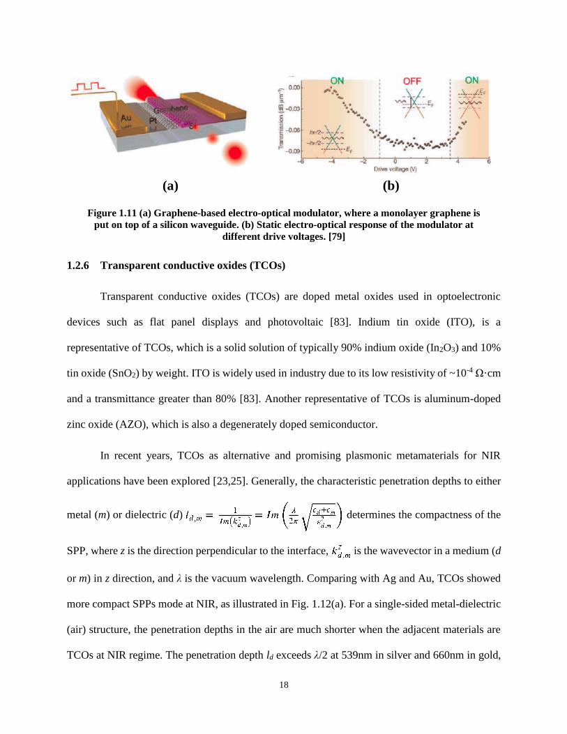
1.2.6 Transparent conductive oxides (TCOs)
Transparent conductive oxides (TCOs) are doped metal oxides used in optoelectronic
devices such as flat panel displays and photovoltaic [83]. Indium tin oxide (ITO), is a
representative of TCOs, which is a solid solution of typically 90% indium oxide (In2O3) and 10%
tin oxide (SnO2) by weight. ITO is widely used in industry due to its low resistivity of ~10-4 Ω·cm
and a transmittance greater than 80% [83]. Another representative of TCOs is aluminum-doped
zinc oxide (AZO), which is also a degenerately doped semiconductor.
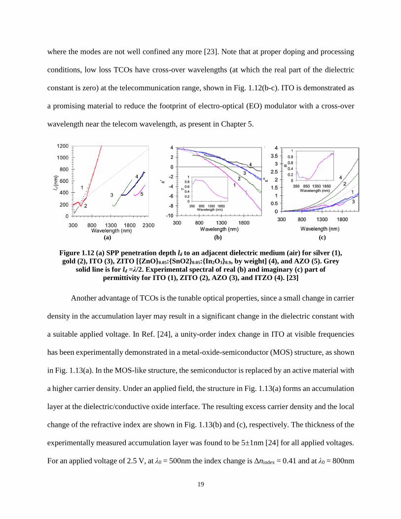
In recent years, TCOs as alternative and promising plasmonic metamaterials for NIR
applications have been explored [23,25]. Generally, the characteristic penetration depths to either
metal (m) or dielectric (d) determines the compactness of the
SPP, where z is the direction perpendicular to the interface, is the wavevector in a medium (d
or m) in z direction, and λ is the vacuum wavelength. Comparing with Ag and Au, TCOs showed
more compact SPPs mode at NIR, as illustrated in Fig. 1.12(a). For a single-sided metal-dielectric
(air) structure, the penetration depths in the air are much shorter when the adjacent materials are
TCOs at NIR regime. The penetration depth ld exceeds λ/2 at 539nm in silver and 660nm in gold,
(a) (b)
19
where the modes are not well confined any more [23]. Note that at proper doping and processing
conditions, low loss TCOs have cross-over wavelengths (at which the real part of the dielectric
constant is zero) at the telecommunication range, shown in Fig. 1.12(b-c). ITO is demonstrated as
a promising material to reduce the footprint of electro-optical (EO) modulator with a cross-over
wavelength near the telecom wavelength, as present in Chapter 5.
Figure 1.12 (a) SPP penetration depth ld to an adjacent dielectric medium (air) for silver (1),
gold (2), ITO (3), ZITO [ZnO0.05:SnO20.05:In2O30.9, by weight] (4), and AZO (5). Grey
solid line is for ld =λ/2. Experimental spectral of real (b) and imaginary (c) part of
permittivity for ITO (1), ZITO (2), AZO (3), and ITZO (4). [23]
Another advantage of TCOs is the tunable optical properties, since a small change in carrier
density in the accumulation layer may result in a significant change in the dielectric constant with
a suitable applied voltage. In Ref. [24], a unity-order index change in ITO at visible frequencies
has been experimentally demonstrated in a metal-oxide-semiconductor (MOS) structure, as shown
in Fig. 1.13(a). In the MOS-like structure, the semiconductor is replaced by an active material with
a higher carrier density. Under an applied field, the structure in Fig. 1.13(a) forms an accumulation
layer at the dielectric/conductive oxide interface. The resulting excess carrier density and the local
change of the refractive index are shown in Fig. 1.13(b) and (c), respectively. The thickness of the
experimentally measured accumulation layer was found to be 5±1nm [24] for all applied voltages.
For an applied voltage of 2.5 V, at λ0 = 500nm the index change is Δnindex = 0.41 and at λ0 = 800nm
(a) (b) (c)
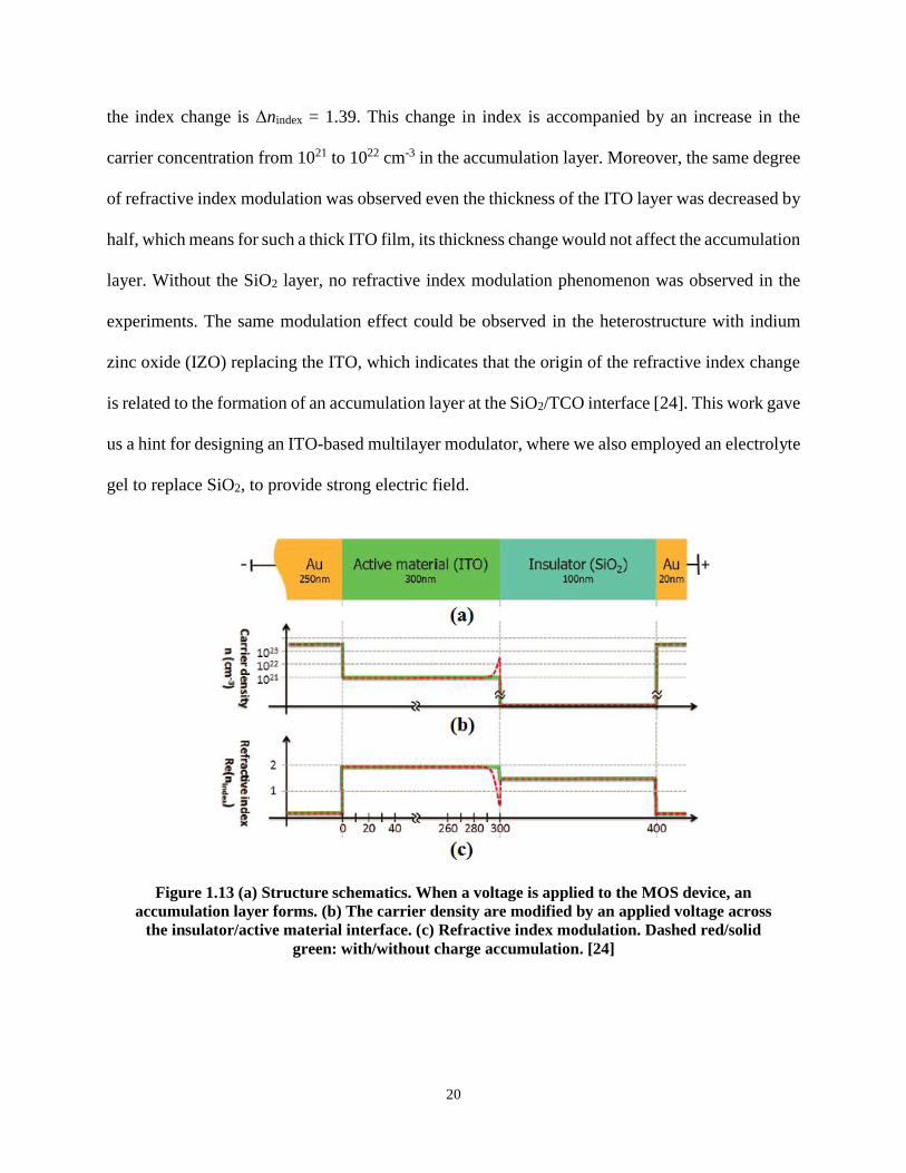
20
the index change is Δnindex = 1.39. This change in index is accompanied by an increase in the
carrier concentration from 1021 to 1022 cm-3 in the accumulation layer. Moreover, the same degree
of refractive index modulation was observed even the thickness of the ITO layer was decreased by
half, which means for such a thick ITO film, its thickness change would not affect the accumulation
layer. Without the SiO2 layer, no refractive index modulation phenomenon was observed in the
experiments. The same modulation effect could be observed in the heterostructure with indium
zinc oxide (IZO) replacing the ITO, which indicates that the origin of the refractive index change
is related to the formation of an accumulation layer at the SiO2/TCO interface [24]. This work gave
us a hint for designing an ITO-based multilayer modulator, where we also employed an electrolyte
gel to replace SiO2, to provide strong electric field.
Figure 1.13 (a) Structure schematics. When a voltage is applied to the MOS device, an
accumulation layer forms. (b) The carrier density are modified by an applied voltage across
the insulator/active material interface. (c) Refractive index modulation. Dashed red/solid
green: with/without charge accumulation. [24]
21
1.3 Fabrication of Metamaterial Samples
Since metamaterials gain the novel properties based on their artificial structures, the
fabrication schemes are determined by the functionalities as well as the working frequencies of
interest of the metamaterials. Hence, metamaterials could be fabricated in a cleanroom by a series
of nano fabrication processes [84], or in a machine shop patterning periodic features [85], or even
with electronic textile technology to build 3D cubic structure [86]. In this section, a general
introduction of fabrication methods of man-made metamaterials will be presented, as well as those
of the naturally existing metamaterials – graphene and ITO.
1.3.1 Metamaterial with artificially designed structures
At the early stage, metamaterials were experimentally demonstrated at microwave
frequency regime, because it is relatively easy and straightforward to construct resonant elements
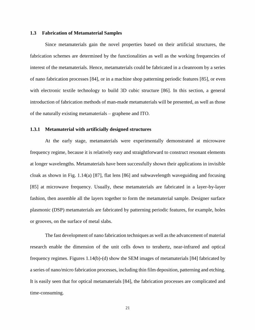
at longer wavelengths. Metamaterials have been successfully shown their applications in invisible
cloak as shown in Fig. 1.14(a) [87], flat lens [86] and subwavelength waveguiding and focusing
[85] at microwave frequency. Usually, these metamaterials are fabricated in a layer-by-layer
fashion, then assemble all the layers together to form the metamaterial sample. Designer surface
plasmonic (DSP) metamaterials are fabricated by patterning periodic features, for example, holes
or grooves, on the surface of metal slabs.
The fast development of nano fabrication techniques as well as the advancement of material
research enable the dimension of the unit cells down to terahertz, near-infrared and optical
frequency regimes. Figures 1.14(b)-(d) show the SEM images of metamaterials [84] fabricated by
a series of nano/micro fabrication processes, including thin film deposition, patterning and etching.
It is easily seen that for optical metamaterials [84], the fabrication processes are complicated and
time-consuming.
22
Figure 1.14 (a) Microwave invisible cloaks [87]. (b) Terahertz metamaterial [88]. (c) and (d)
Optical metamaterials. [84]
1.3.2 Graphene synthesis, transfer and characterization
In order to practically implement graphene to devices, reliable, stable and economical
process techniques should be developed. One of the most successful methods that results in
isolation of single layer graphene (SLG) is the mechanical exfoliation [89]. Beside the mechanical
exfoliation, other promising techniques as epitaxial growth on metal substrates [68,90-92,94],
epitaxial growth on silicon carbide [94,95], growth from metal-carbon melts [69], and chemical
synthesis [96,97]. Figure 1.15 illustrates some of these methods, their cost and the quality of
graphene film synthesized by each corresponding method.

23
Figure 1.15 Several methods of mass-production of graphene, which allow a wide choice in
terms of size, quality and price for any specific application. [64]
Epitaxial growth of graphene on metal substrates uses the atomic structure of metal
substrates to seed the growth of the graphene [68,90-92,94]. Ni and Cu thin films deposited on top
f SiO2/Si wafers are usually used as the substrate. After the graphene growth, instantaneous etching
of metal films and polymer-supported transfer onto other substrates are followed. These methods
are using mixed gas of Methane, Hydrogen, Argon or Helium in a high temperature furnace for
the growth of graphene. It is shown that mono- and bi-layer graphene grows predominantly on a
Cu substrate, while on Ni, the layers of graphene range from three to eight, which depends on the
reaction time and cooling rate [90]. Cooling rate significantly affects the amount and quality of the
carbon segregated on the metal substrates. With a 10ºC/s cooling rate, high quality graphene with
well-controlled thickness can form on a Ni substrate.
Large and homogeneous layers of graphene can also be obtained by annealing silicon
carbide in a dense noble gas atmosphere, so silicon will sublimate from SiC surface. During the

24
process, graphene nucleates along the plane, which is known as terrace step edges, on the
silicon carbide surface. The nucleation and growth of monolayer graphene on the Si-face of SiC
is highly dependent on growth conditions, SiC surface morphology, and SiC surface defects. The
quality of the graphene films can be improved with a higher synthesis temperature (1425°C) [95].
Graphene may also grow from metal-carbon melts [69]. This process involves dissolving
carbon inside a molten metal at a specified temperature and then allowing the dissolved carbon to
nucleate and grow on top of the melt at a lower temperature. Similarly as the epitaxial growth
methods, Ni and Cu could be used as the molten metal. First, the metal is melt and in contact with
a carbon source. The source could be graphite chunk or powder temperature results in dissolution
and saturation of carbon atoms in the melt. Upon lowering the temperature, the solubility of carbon
in the molten metal decreases and the excess amount of carbon precipitates on top of the metal.
High-quality single layer graphene is obtained in the Ni melt [69].
Graphene can be produced by direct chemical synthesis. Common laboratory reagents
ethanol and sodium are used and single layer graphene is synthesized by low-temperature flash
pyrolysis of solvothermal product of the two reagents, followed by gentle sonication of the
nanoporous carbon product [96]. Graphene nanoribbons (GNR) with width below 10nm are
solution-phase-derived, stably suspended in solvents with noncovalent polymer fictionalization,
and exhibited ultra-smooth edges with possibly well-defined zigzag or armchair-edge structure
[97].
Graphene-transferring process is a key as well as challenging step in the fabrication of
devices [98-100], since the thin graphene film is very delicate and easily broken during the process.
The process shown in Fig. 1.16 is the as-grown graphene transferring to a desired substrate in a

25
step-by-step fashion. The graphene sample is synthesized by chemical vapor deposition (CVD)
technique [68,69]. Polymethyl-methacrylate (PMMA) as a supporting and protection layer will be
coated on top of graphene. Then the PMMA/graphene/nickel/SiO2/Si chip will be immersed into
buffered oxide etch (BOE) solution to etch SiO2 layer first. After the long etching process in BOE,
the film will be transferred to FeCl3 solution to remove nickel residue. The following step after the
transfer (shown in Fig. 1.16(b)) is to remove the PMMA by acetone. Then the graphene sheet on
the target substrate will be rinsed in IPA and dry. Figure 1.16(c) shows the ‘active’ graphene after
lithography/oxygen plasma etching, in which the graphene region is 11μm long in the light
propagation direction.
Figure 1.16 (a) Process for transferring as-grown graphene to a desired target. (b) PMMA-
supported graphene on the target. (c) After oxygen etching, the graphene region is
highlighted by the yellow dashed lines.
Accurately determining the numbers of layer of a graphene sample is critical for its
applications. Raman spectroscopy is a noncontact, reflective technique, which provides a fast,
nondestructive means of determining layer thickness of graphene thin films. The Raman spectrum
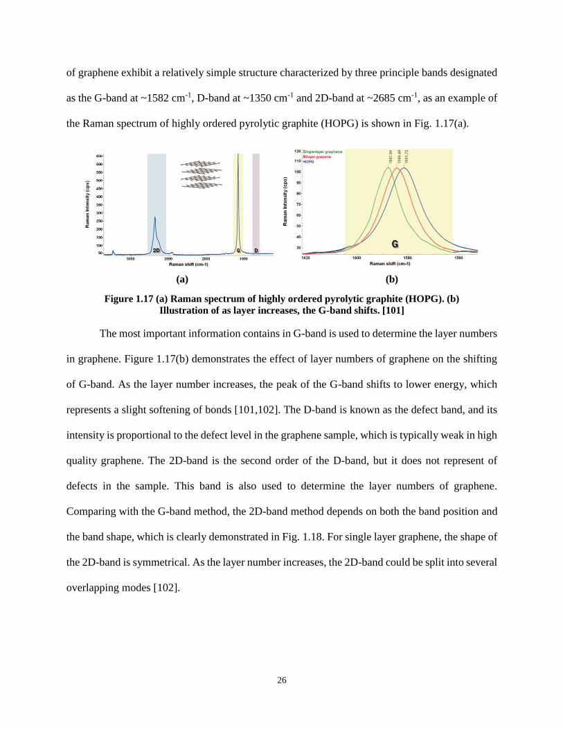
26
of graphene exhibit a relatively simple structure characterized by three principle bands designated
as the G-band at ~1582 cm-1, D-band at ~1350 cm-1 and 2D-band at ~2685 cm-1, as an example of
the Raman spectrum of highly ordered pyrolytic graphite (HOPG) is shown in Fig. 1.17(a).
Figure 1.17 (a) Raman spectrum of highly ordered pyrolytic graphite (HOPG). (b)
Illustration of as layer increases, the G-band shifts. [101]
The most important information contains in G-band is used to determine the layer numbers
in graphene. Figure 1.17(b) demonstrates the effect of layer numbers of graphene on the shifting
of G-band. As the layer number increases, the peak of the G-band shifts to lower energy, which
represents a slight softening of bonds [101,102]. The D-band is known as the defect band, and its
intensity is proportional to the defect level in the graphene sample, which is typically weak in high
quality graphene. The 2D-band is the second order of the D-band, but it does not represent of
defects in the sample. This band is also used to determine the layer numbers of graphene.
Comparing with the G-band method, the 2D-band method depends on both the band position and
the band shape, which is clearly demonstrated in Fig. 1.18. For single layer graphene, the shape of
the 2D-band is symmetrical. As the layer number increases, the 2D-band could be split into several
overlapping modes [102].
(a) (b)

27
Figure 1.18 The significant different band shapes (red curves) of 2D-band with the number of
layers on each. [102]
1.3.3 ITO deposition and annealing
The optical property of ITO mainly depends on its deposition and post-deposition
annealing conditions, which includes the ambient gases and the temperature [103]. The deposition
method could either be sputtering or laser ablation [104]. In Semiconductor & Microsystems
Fabrication Laboratory (SMFL) of RIT, ITO thin film can be deposited by sputtering process with
CVC601. The basic idea of sputtering is using accelerated particles to bombard the target and
knock the target atoms out. Then these free atoms will be deposited on the surface of the substrate.
During the sputtering process, plasma is usually used since it contains charged particles, this low-
pressure gas is easily directed by electric fields. To obtain plasma, a voltage will be applied on a
pair of electrodes. Free electrons which gain energy from the electric fields will collide with gas
particles, eventually cause ionization. This is known as direct-current (DC) glow discharge [105].
The sputtering process using a (In2O3)0.9(SnO2)0.1 weight percentage target, was done at room
temperature and at 7.3mTorr pressure within the chamber. Argon is the only gas used in the
deposition process. With a deposition time of 12 mins, the ITO thin film has a high sheet resistance
around 3000 ~ 4000 Ω/. And the thickness of ITO film is measured and turned out in the range
of 22-25nm.
Significant changes in the conductivity of ITO film can be observed with post-deposition
annealing process in different ambient, for example, film annealed in nitrogen showed more
(a) Single layer
(b) Two layers
(c) Three layers
(d) Multilayers

28
conductive and in oxygen less conductive but more transparent [106]. In Ref. [107], the change of
the dielectric function of the e-beam evaporated ITO film is observed with different annealing
ambient environments, as shown in Fig. 1.19. A higher annealing temperature increases the
conductivity of ITO film and reduces the loss within the wavelength range of interest [107]. The
post-annealing process is carried out in a vacuum oven – Heraeus oven – at 350°C for 4 hours.
After the annealing process, the sheet resistance of the ITO film decreased significantly, which
was in the range of 60-100Ω/. The optical property of the ITO film will be introduced in Chapter
5.
Figure 1.19 Real (a) and imaginary (b) parts of permittivity of ITO annealed at various
conditions (N2, 450°C; N2, 650°C; O2, 450°C; O2, 650°C). [107]
1.4 Finite-Difference Time-Domain (FDTD) Modeling
The FDTD method [108] is one of the most important and effective numerical methods to
study metamaterials, which was proposed by Yee in 1966 [109]. Since FDTD is a time domain
solver, it is convenient to investigate the characteristics of metamaterials over a wide frequency
regime. The basic idea of Yee algorithm is simultaneously dealing with both electric and magnetic

29
fields in time and space using coupled form of Maxwell’s curl equations. The Maxwell’s curl
equations in linear, isotropic, nondispersive materials can be written as
(1.5)
(1.6)
where σ* is equivalent magnetic loss, σ is the electric conductivity, is the electric field, is the
magnetic field, ε is the medium permittivity and μ is the permeability. Expanding the vector
components of the curl operators of Eq. (1.5) and (1.6) yields the following six coupled scalar
equations under Cartesian coordinate, which are the basis of the FDTD numerical algorithm for
modeling electromagnetic wave interactions with arbitrary three-dimensional objects [110]
(1.7)
(1.8)
(1.9)
(1.10)
(1.11)
(1.12)
In Yee’s algorithm, and components are positioned at the centers of the grid lines and
surfaces such that each component is surrounded by four components, and vice versa, as
shown in Fig. 1.20.

30
Figure 1.20 Yee’s spatial grid. (Internet)
In Yee’s algorithm, all of the components in the modeled space are computed and stored
in memory by using the previously computed values of and the newly updated field data. In
the next step, is recomputed in a similar way. This process stops when the time-stepping is
terminated [110].
In order to get numerical stability of the Yee algorithm, an upper bound on the time step
Δt should be set, which is determined by the spatial increments Δx, Δy, Δz in accordance with the
Courant-Friedrich-Levy (CFL) stability condition [110]. In three dimensions the condition is given
by
(1.13)
1.5 Dissertation Overview
This dissertation presents numerical and experimental results of novel metamaterials and
their applications in subwavelength waveguiding, imaging and modulating. These results are
structured as follows.

31
Chapter 2 presents the motivation, numerical modeling and the experimental
demonstration of a metal grating functioning as a designer surface plasmonic waveguide, which
can support deep subwavelength surface modes and the width of the modes can be squeezed also
into deep subwavelength by tapering the width of the waveguide.
Chapter 3 introduces a re-visit of classical optical phenomenon – Talbot effect, in indefinite
metamaterial. The 2D and 3D numerical simulations show that the “super” Talbot effect can be
achieved in the indefinite metamaterial, even without the paraxial approximation.
Chapter 4 presents the numerical modeling of optical switch based on a metal-insulator-
metal plasmonic waveguide with Si3N4 core sandwiched between two gallium (Ga) metal layers.
Combing the unique structural phase transition property of gallium, within a total length of 400nm,
an extinction ratio as high as 7.68 dB can be achieved in the proposed nanoplasmonic structure.
Chapter 5 proposes active plasmonic metamaterials for electro-optical modulator
applications. When applying external voltages on these ITO-based multilayer structures, electric
double layers are formed at the interfaces of ITO and electrolyte gel. Based on attenuated total
reflection (ATR) measurement results, modulation depth up to 38.8% can be achieved. Preliminary
result is present for the real time response of an ITO/electrolyte gel/doped-Si modulator.
Chapter 6 continues the work in Chapter 5 and investigates a novel waveguide, namely
“TCO-slot waveguide”, which combines both the tunable property of a TCO and field
enhancement of a slot waveguide. In this work, light absorption can be sharply enhanced when the
slot dielectric constant is tuned close to zero. Based on TCO-slot waveguides, efficient electro-
absorption modulation can be achieved within 200nm with small insertion loss.
32
Chapter 7 experimentally demonstrates greatly enhanced light absorption by monolayer
graphene over a broad spectral range, from visible to near infrared, based on the attenuated total
reflection. In the experiment, graphene is sandwiched between two dielectric media referred as
superstrate and substrate. Based on numerical calculation and experimental results, the closer the
refractive indices of the superstrate and the substrate, the higher the absorption of graphene will
be. The light absorption of monolayer graphene up to 42.7% is experimentally achieved.
Chapter 8 continues the work in Chapter 7 and presents the recent exploration of graphene
electro-optic modulators based on graphene sandwiched in dielectric or plasmonic waveguides.
With a suitable gate voltage, the dielectric constant of graphene can be tuned to be very small due
to the effect of intraband electronic transition, resulting in “graphene-slot waveguides” and greatly
enhanced absorption modes. Up to 3 dB modulation depth can be achieved within 800nm long
silicon waveguides, or 120nm long plasmonic waveguides based on three-dimensional numerical
simulations.
Chapter 9 summarizes work as well as an outlook for future work.
Chapter 10 lists all the publications.
1.6 Contributions
The following are the main contributions of this dissertation.
1) We propose to use microwave near-field imaging system, which is known to be the
first time this method is used to study designer surface plasmons. The fundamental
work can be extended to design DSP devices at THz frequency regime.

33
2) We explore the novel effects of light propagation in indefinite metamaterials and
propose the applications in various operational settings, i.e. lithography, optical
storage, and imaging system.
3) We investigate the epsilon-near-zero (ENZ) properties of natural materials – graphene
and ITO, combining novel slot waveguides as the platform to propose ultra-compact,
efficient electro-optical modulators.
4) We experimentally demonstrate the absorption of monolayer graphene can be
significantly enhanced over a broad spectral range, where there is no complicated,
time-consuming fabrication process involved.
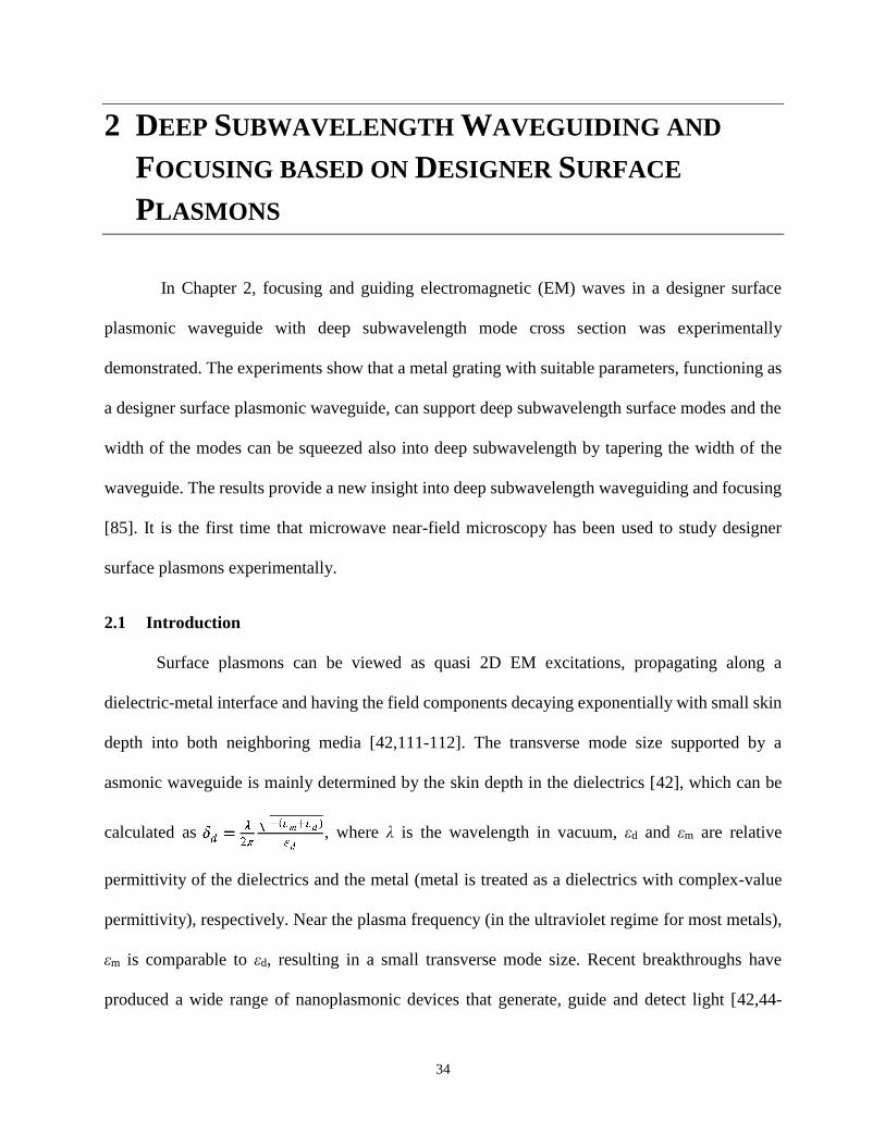
34
2 DEEP SUBWAVELENGTH WAVEGUIDING AND
FOCUSING BASED ON DESIGNER SURFACE
PLASMONS
In Chapter 2, focusing and guiding electromagnetic (EM) waves in a designer surface
plasmonic waveguide with deep subwavelength mode cross section was experimentally
demonstrated. The experiments show that a metal grating with suitable parameters, functioning as
a designer surface plasmonic waveguide, can support deep subwavelength surface modes and the
width of the modes can be squeezed also into deep subwavelength by tapering the width of the
waveguide. The results provide a new insight into deep subwavelength waveguiding and focusing
[85]. It is the first time that microwave near-field microscopy has been used to study designer
surface plasmons experimentally.
2.1 Introduction
Surface plasmons can be viewed as quasi 2D EM excitations, propagating along a
dielectric-metal interface and having the field components decaying exponentially with small skin
depth into both neighboring media [42,111-112]. The transverse mode size supported by a
asmonic waveguide is mainly determined by the skin depth in the dielectrics [42], which can be
calculated as , where λ is the wavelength in vacuum, εd and εm are relative
permittivity of the dielectrics and the metal (metal is treated as a dielectrics with complex-value
permittivity), respectively. Near the plasma frequency (in the ultraviolet regime for most metals),
εm is comparable to εd, resulting in a small transverse mode size. Recent breakthroughs have
produced a wide range of nanoplasmonic devices that generate, guide and detect light [42,44-

35
47,50,51,113,114]. However, far below plasma frequency, εm is approximately a pure imaginary
number with large magnitude, resulting in a very large transverse mode size (~102λ and ~103λ in
the THz and microwave regimes, respectively). This limits some important applications of surface
plasmons, especially in the THz regime, where deep subwavelength optical devices will be a
critical technique for the integration of THz, photonic, and electronic circuits on the same chip
using the CMOS compatible technology.
Nevertheless, this issue can be addressed by plasmonic metamaterials, where the dispersion
of surface plasmons and spatial confinement of waves can be engineered by designed surface
textures. This approach can date back to Goubau [43], and Mills and Maradudin [52], who
discovered that a surface texture on metal, such as arrays of holes or grooves, can result in highly
bounded surface waves. In 2004 and 2005, researchers established their similarity with surface
plasmons and referred them to as “designer surface plasmons” or “spoof surface plasmons” [54-
55]. The existence of designer surface plasmons has recently been verified both in the microwave
and THz regimes [56,58,115]. More recently, significant progress has been made on designer
surface plasmonic (DSP) devices using various types of surface textures [59-63,116]. However,
most of effort has been focused on numerical investigations and the importance of designer surface
plasmons is far from being demonstrated. Herein, we demonstrate the remarkable advantages of
using the designer surface plasmons for deep subwavelength waveguiding and focusing.
2.2 Design and Fabrication
2.2.1 Modeling
The main structures involved in our work are simply metal gratings, specifically aluminum
slabs patterned with an array of rectangular grooves. The metal gratings as DSP waveguides were
investigated more recently [53,63]. Assume the width, length and depth of each groove are w, a

36
and h, and the period of the array is d. Pendry’s pioneering work shows that a simple metal grating
can work well as a DSP waveguide [54].
If only the fundamental TM-like mode (magnetic field H is parallel to the groove
orientation) is considered, the dispersion of EM waves propagating in the DSP waveguide can be
described as [45]
(2.1)
where , 𝛽 , β is the propagation constant, and k0 is the wave
number in free space. The dispersion curve is similar to that of widely investigated dielectric-metal
plasmonic waveguides in the near infrared or visible regimes. When or equivalently ≈
, β reaches its maximum. Therefore, the surface structure can “shift” the effective plasma
frequency of the textured metal into any region closer to working frequency and achieve much
stronger mode binding. More precisely, due to the interference of multiple waves on the surface
texture, a tightly bounded mode can be formed on the surface. In particular, based on the dispersion
relation, such a metal grating can be roughly equivalent as an h-thick layer of homogeneous but
anisotropic medium on PEC when a << d << λ [53]. Consequently, if only the first order diffraction
is considered, the skin depth over the grating can be estimated as
(2.2)
which can be on the deep subwavelength scale. Moreover, due to the tight binding of surface waves,
the decrease of the width of the grating will reduce the mode size in another transverse direction,
yet not significantly alter the dispersion of the guided modes [63]. An extreme case is that the
surface texture is converted into a series of aligned rods, which can guide EM waves at ultra-deep

37
subwavelength scale in both transverse directions. Essentially, the aligned rods form a 3D deep
subwavelength DSP waveguide, similar as arrays of nanoparticles forming nanoplasmonic
waveguides in the visible light regime [44,116].
2.2.2 Fabrication and experimental setup
The 2D and 3D DSP waveguides are designed to work at microwave regime by patterning
arrays of periodic surface textures on an aluminum slabs. The structure designs are using 3D CAD
software SolidWorks and the fabrication is finished by Brinkman Machine Tools and
Manufacturing Laboratory at RIT. Figure 2.1 shows some pictures of the designer surface
plasmonic waveguides. The main parameters of the 3D waveguide shown in Fig. 2.1(a) are: period
d=12.7mm, metal rod length a=6.35mm, width w=6.35mm, height h=19.05mm. A directional
coupler is formed by aligning two identical 3D waveguides, as illustrated in Fig. 2.1(b). For the
tapered waveguide, input 2D waveguide width W=203mm, tapered region length L=216mm. The
parameters of the 3D waveguide are the same as those shown in Fig. 2.1(a).
Figure 2.1 (a) 3D DSP waveguide. (b) Two identical 3D waveguides are aligned and forming a
directional coupler. (c) Tapered DSP waveguide with a 2D waveguide as input. [85]
To experimentally explore its performance, a microwave near-field measurement setup
based on a vector network analyzer was built [9,117,118] as shown in Fig. 2.2, where the
propagation of EM waves in a waveguide can be measured by the raster scan of a 1-mm microwave

38
monopole to detect the evanescent tails. One monopole was fed as the source and another was used
as the detector. The movement of the detector in x and y directions was controlled by a motion
controller. In order to show the mode profiles rather than in x-y plane, a manual stage (along z-axis
moving range: 25mm, minimum resolution: 0.025mm) was used in the experiments to control the
movement of the detector in z direction. The precise control of the motion of the detector and the
small size of the detector ensured that the experimental results were reliable [119]. To get accurate
results, the maximum pixel size was set to be 0.5mm by 0.5mm in the measurements related to the
calculations of mode sizes along different directions. Both the amplitude and phase of each
measurement point were recorded by the E8362A PNA vector network analyzer.
Figure 2.2 Experimental setup based on VNA and XYZ stages.
2.3 Experimental results and analysis
2.3.1 3D DSP waveguide
Figure 2.3 plots the dispersion diagram of the supported modes. When the working
frequency varies from 1.4 GHz to 3.3 GHz, the effective index of the corresponding guided modes
increases, and then jumps to the second band starting at 8.39 GHz, which is not shown in the figure.

39
Compared with the dispersion relation of the 2D DSP modes (infinite width), the finite width of
the 3D DSP waveguide imposes a lower-side cutoff frequency when the dispersion curve is located
inside the light cone. After a raster-scan of the detector at different locations over the structure,
good guided modes at frequencies between 1.5 GHz and 3.5 GHz were observed, which
respectively coincide with the lower and upper cutoffs of the numerical results as shown in Fig.
2.3. Furthermore, according to the phase distribution along the waveguide, we can calculate the
propagation constants at different frequencies. As shown in Fig. 2.3, the measured dispersion curve
is in good agreement with the simulated one. Figure 2.4 shows the intensity of the mode profile in
different directions at f = 2.25GHz. Figure 2.4(a) is the fabricated 3D DSP waveguide. As shown
in Figs. 2.4(b)-2.4(d), the guided mode is tightly “nailed” on the metal rods of the grating and
slightly diverges between the rods. The slightly beating of the intensity shown in Fig. 2.4(d) is due
to the back reflection. The maximum of the mode size can be mapped in the middle plane of two
neighboring rods. The mode size slightly varies with different frequencies and minimizes at
5.5mm-by-4.5mm (or 0.04λ-by-0.03λ) by intensity full width at half maximum (FWHM) at 2.25
GHz, as shown in Fig. 2.4(e). Over the metal rod, the mode size is 7.00mm-by-1.00mm as shown
in Fig. 2.4(c). And the mode size measured along the side wall of the rod shown in Fig. 2.4(f) is
15mm-by-1.3mm. Therefore, the overall mode size relies on the dimensions of rods and can go
into the deep subwavelength scale.
40
Figure 2.3 The dispersion diagram of DSP waveguides. The parameters of the waveguides are
d = 12.7mm, a = 6.35mm, and h = 19.05mm. The width of the 2D DSP waveguide is assumed
to be infinite; the width of the 3D DSP waveguide is w = 6.35mm. The circles indicate the
measured dispersion relation for the 3D DSP waveguide. [85]
Theoretically, the propagation loss is very small because the 3D DSP waveguide supports
a guided mode with small effective index (neff =1.2 at f=2.25GHz) and the small mode size
supported by the waveguide is due to the interference of surface waves. The propagation
attenuation mainly comes from the scattering due to fabrication imperfection. In our microwave
device, the attenuation is very small and cannot be accurately measured within a short propagation
distance.

41
Figure 2.4 (a) The fabricated 3D DSP waveguide. The measured mode profiles (shown in
normalized intensity) in different directions: (b) Side (over rods, in x-z plane), (c) Cross
section over a rod (in y-z plane), (d) Top view (over rods, in x-y plane), the dashed blue
squares indicate the positions of the metal rods, (e) Cross section in a groove (in y-z plane), (f)
Cross section along the side wall of a rod (in y-z plane). [85]
2.3.2 3D directional coupler
To further demonstrate the function of the metal grating as a deep subwavelength DSP
waveguide, we aligned two identical waveguides in parallel and formed a directional coupler as
shown in Fig. 2.5(a). The EM source was then fed from one of the waveguides. Figure 2.5(b)
shows that the EM wave switches between the waveguides at f = 3.25GHz. The distance between
the two identical waveguides is 12.7mm (from center to center).
Figure 2.5 (a) Two DSP waveguides in parallel form a directional coupler. (b) The EM wave
(shown in normalized amplitude) propagates in the directional coupler. [85]
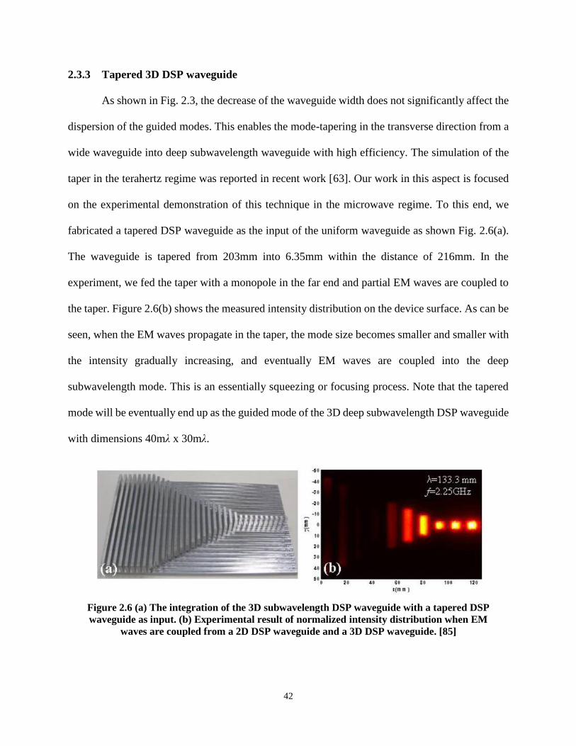
42
2.3.3 Tapered 3D DSP waveguide
As shown in Fig. 2.3, the decrease of the waveguide width does not significantly affect the
dispersion of the guided modes. This enables the mode-tapering in the transverse direction from a
wide waveguide into deep subwavelength waveguide with high efficiency. The simulation of the
taper in the terahertz regime was reported in recent work [63]. Our work in this aspect is focused
on the experimental demonstration of this technique in the microwave regime. To this end, we
fabricated a tapered DSP waveguide as the input of the uniform waveguide as shown Fig. 2.6(a).
The waveguide is tapered from 203mm into 6.35mm within the distance of 216mm. In the
experiment, we fed the taper with a monopole in the far end and partial EM waves are coupled to
the taper. Figure 2.6(b) shows the measured intensity distribution on the device surface. As can be
seen, when the EM waves propagate in the taper, the mode size becomes smaller and smaller with
the intensity gradually increasing, and eventually EM waves are coupled into the deep
subwavelength mode. This is an essentially squeezing or focusing process. Note that the tapered
mode will be eventually end up as the guided mode of the 3D deep subwavelength DSP waveguide
with dimensions 40mλ x 30mλ.
Figure 2.6 (a) The integration of the 3D subwavelength DSP waveguide with a tapered DSP
waveguide as input. (b) Experimental result of normalized intensity distribution when EM
waves are coupled from a 2D DSP waveguide and a 3D DSP waveguide. [85]
43
2.4 Conclusions
Compared to most theoretical work in designer surface plasmonic metamaterials [59-
63,116], in this work, metal grating as a deep subwavelength DSP waveguide is experimentally
investigated, where mode cross section down to 40mλ x 30mλ can be achieved in air. An efficient
coupler for the deep subwavelength waveguide is also demonstrated, which provides a means to
squeeze or focus EM waves into the deep subwavelength scale. It is worth noting that the modeling
of the devices is based on perfect electric conductor (PEC) for metal and hence there is no difficulty
to be scaled down into the THz regime, where metal can still be roughly treated as a PEC.
In addition, the working wavelength is scalable with the index of the surrounding medium
as opposed to air. This is evident that when we immersed the device in low loss oil with refractive
index nd ≈ 2, the working frequency shifted to approximate half of its original value. Thus, the
mode size to wavelength ratio is inversely proportional to the refractive index. In particular, the
mode size can be further shrunk into 0.01λ0-by-0.02λ0 (λ0 is the wavelength in free space), if silicon
(nd ≈ 3.5) is coated on a 3D DSP waveguide in the THz regime. In Ref. [120], with silicon (at 0.6
THz) or germanium (at MIR region of 30 THz), numerical modeling via 3D FDTD has shown
deep sub-wavelength mode confinement in transverse directions to smaller than λ/50 by λ/50, with
an estimated propagation loss of less than 0.1 dB for each repetitive unit.

44
3 SUPER TALBOT EFFECT IN INDEFINITE
ANISOTROPIC METAMATERIAL
In Chapter 2, an image size of 0.04λ-by-0.03λ can be achieved by metal gratings
functioning as designer surface plasmonic (DSP) waveguide at microwave frequencies. In this
chapter, we will re-visit a classical optical phenomenon named as Talbot effect and see that a
comparable image size (~0.087λ0) can be obtained at visible frequency via indefinite metamaterial.
The Talbot effect (or the self-imaging effect) can be observed for a periodic object with a pitch
larger than the diffraction limit of an imaging system, where the paraxial approximation is applied.
The “super” Talbot effect can be achieved in an indefinite metamaterial even when the period is
much smaller than the diffraction limit in both two-dimensional (2D) and three-dimensional (3D)
numerical simulations, where the paraxial approximation is not applied. This is attributed to the
evanescent waves, which carry the information about subwavelength features of the object, can be
converted into propagating waves and then conveyed to far field by the metamaterial, where the
permittivity in the propagation direction is negative while the transverse ones are positive. The
indefinite metamaterial can be approximated by a system of thin, alternating multilayer metal and
insulator (MMI) stack. As long as the loss of the metamaterial is small enough, deep
subwavelength image size (~0.087λ0) can be obtained in the super Talbot effect [121].
3.1 Introduction
3.1.1 TE and TM waves
In the electromagnetic waves, both the electric field and the magnetic field are oscillating
in different directions. The polarization of the EM wave refers to the direction of the electric field.
In parallel polarization, also known as p-polarization, or TM polarization, the electric fields lie on

45
the plane of incidence and the magnetic fields are perpendicular to that plane (along y-direction)
and transverse to the z-direction, as shown in Fig. 3.1(a). In perpendicular polarization, which is
also known as s-polarization, or TE polarization, the electric fields are perpendicular to the plane
of incidence (along y-direction) and transverse to the z-direction, and the magnetic fields lie on
that plane, shown in Fig. 3.1(b).
Figure 3.1 Illustration of oblique incidence for (a) TM- and (b) TE-polarized light.
Now we consider that the interface shown in Fig. 3.1(a) and (b) is between a dielectric and
a metal, shown as Fig. 3.2(a). We will apply Maxwell’s equations in Eq. (3.1a-d) to the flat
interface and investigate the physical properties of surface plasmon polaritons (SPPs) [41,42],
which is known as electromagnetic excitations propagating at the interface and evanescently
confined perpendicular to the interface. These equations describe how the electric field E and
magnetic field H are generated and altered by each other and by external charge density ρ and
current density J.
(3.1a)

46
(3.1b)
× (3.1c)
× (3.1d)
Figure 3.2 (a) Illustration of a SPPs as a collective excitation at a metal-dielectric interface.
The electric field E and magnetic field H are enhanced at the interface. (b) The perpendicular
field Ez decays exponentially with a characteristic length δd in the dielectric and δm in metal.
[122]
Using the curl Eqs. (3.1c-d), for harmonic time dependence ( ), and propagation
along the x-direction ( ), we can have the following set equations,
(3.2a)
(3.2b)
(3.2c)
(3.2d)
(3.2e)

47
(3.2f)
Equation set (3.2a-c) are the transverse magnetic (TM or p) mode, where only the field components
Ex, Ez and Hy are nonzero, and the second set (3.2d-f) are the transverse electric (TE or s) mode,
with only Hx, Hz and Ey are nonzero.
For TM modes, the equation set can be simplified to
(3.3a)
(3.3b)
and the wave equation for the TM mode is
(3.3c)
For TE modes the equation set is
𝜇
(3.4a)
𝜇
(3.4b)
and the TE wave equation is
(3.4c)
From Eqs. (3.4a-c), for TE mode, the expressions for the field components in half spaces
shown in Fig. 3.2(a) are
(3.5a)
(3.5b)

48
(3.5c)
for and
(3.5d)
(3.5e)
(3.5f)
for . In these equation sets, is the wave component perpendicular to the
interface. From boundary condition – the continuity of Ey and Hx at the interface leads to
(3.6)
To get the confinement at the interface, it requires that and . In Eq. (3.6)
this condition is only fulfilled when , therefore . Hence, there is no surface
mode exists with TE polarization.
On the other hand, for TM polarization, the field expressions are
(3.7a)
(3.7b)
(3.7c)
for and
(3.7d)
(3.7e)
(3.7f)
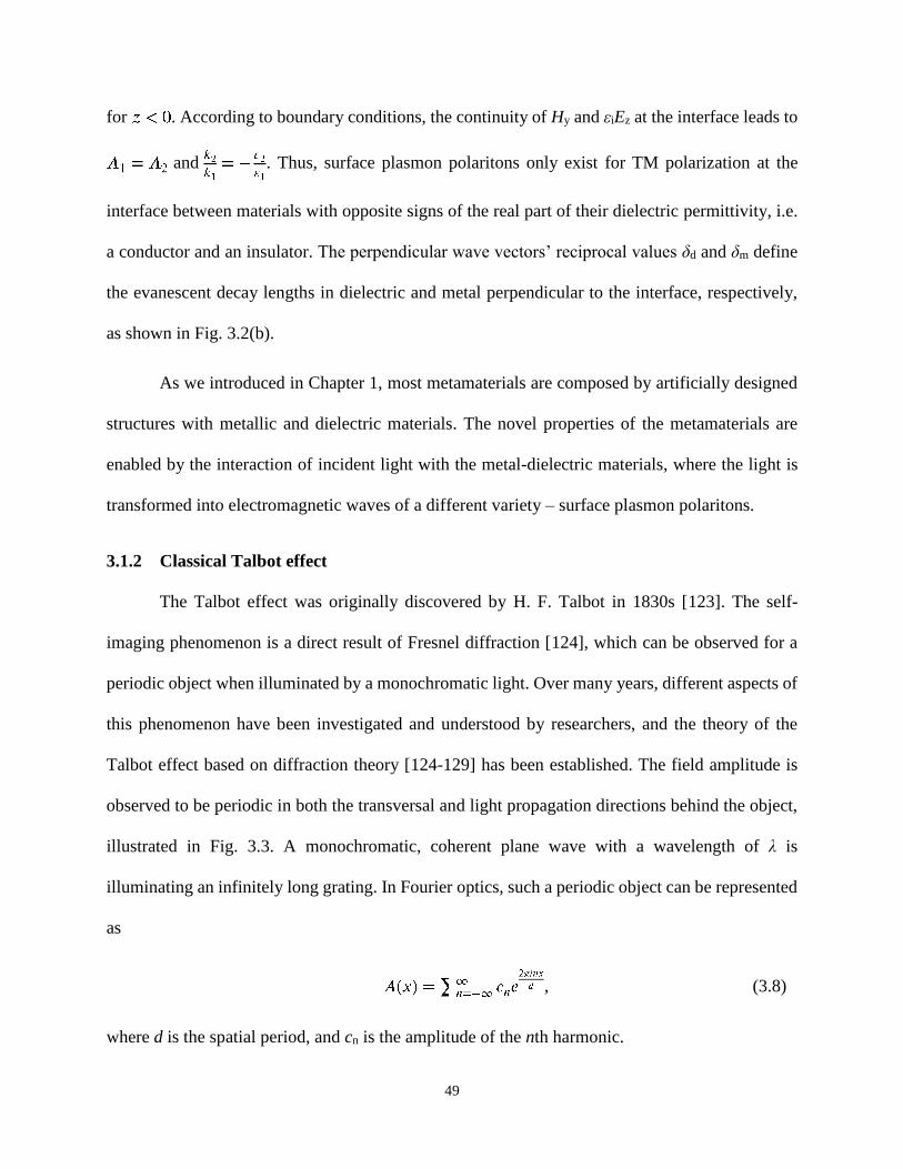
49
for . According to boundary conditions, the continuity of Hy and εiEz at the interface leads to
and . Thus, surface plasmon polaritons only exist for TM polarization at the
interface between materials with opposite signs of the real part of their dielectric permittivity, i.e.
a conductor and an insulator. The perpendicular wave vectors’ reciprocal values δd and δm define
the evanescent decay lengths in dielectric and metal perpendicular to the interface, respectively,
as shown in Fig. 3.2(b).
As we introduced in Chapter 1, most metamaterials are composed by artificially designed
structures with metallic and dielectric materials. The novel properties of the metamaterials are
enabled by the interaction of incident light with the metal-dielectric materials, where the light is
transformed into electromagnetic waves of a different variety – surface plasmon polaritons.
3.1.2 Classical Talbot effect
The Talbot effect was originally discovered by H. F. Talbot in 1830s [123]. The self-
imaging phenomenon is a direct result of Fresnel diffraction [124], which can be observed for a
periodic object when illuminated by a monochromatic light. Over many years, different aspects of
this phenomenon have been investigated and understood by researchers, and the theory of the
Talbot effect based on diffraction theory [124-129] has been established. The field amplitude is
observed to be periodic in both the transversal and light propagation directions behind the object,
illustrated in Fig. 3.3. A monochromatic, coherent plane wave with a wavelength of λ is
illuminating an infinitely long grating. In Fourier optics, such a periodic object can be represented
as
, (3.8)
where d is the spatial period, and cn is the amplitude of the nth harmonic.

50
Figure 3.3 Illustration of the optical Talbot effect, shown as a Talbot carpet. [130]
The diffracted field amplitude E(X) is defined in terms of the amplitude transmission of the
object A(x) and the coherent amplitude of the source S(xs), according to the Fresnel-Kirchhoff
diffraction theory [131], where X, x, and xs are Cartesian coordinates in the observation, object,
and source planes, respectively. In the paraxial approximation, the diffraction amplitude E(X) at a
distance z from the object is proportional to
. (3.9)
By substituting Eq. (3.8) into Eq. (3.9), we can get
(3.10)
At a certain distance z, all diffraction orders are in phase by satisfying the condition
, (3.11)
where m is a positive integer and referred as the self-imaging number, and d is the period of the
diffraction grating. From Eq. (3.11), the Talbot distance is defined as
0 zT/2 zT
Periodic object

51
(3.12)
At z = ZT, the primary Talbot image is observed in Fig. 3.3, and at z =ZT/2 is the Talbot distance
of the secondary Talbot image, where the image has a d/2 shift along the transversal direction. The
fractional Talbot images are observed at all rational multiples of ZT, which can be expressed as
, (3.13)
where p and q are prime integers.
Due to its simple arrangement, the Talbot effect attracts researchers’ interests and the self-
imaging phenomenon has a variety of applications in the optical dispersive fiber system [132,133],
optical computing [134], phase locking of laser arrays [135], and in electron optics and microscopy
[136]. The Talbot effect has also been demonstrated with atomic waves [137], and waveguide
arrays [138,139].
3.1.3 Talbot effect in plasmons
Studying the analogues of the classical optical phenomena is an important aspect of the
development of new branches of optics. Surface plasmon polaritons (SPPs) is well known for their
advantages, for example, they can concentrate the electromagnetic field near the metal/dielectric
interface, therefore enabling compact light waveguiding [140]. In 2007, Dennis and Zheludev, et.
al., first proposed the concept of the plasmon Talbot effect [141]. The analog of the Talbot effect
in plasmons is illustrated in Fig. 3.4(a), where a plane wave is incident from the back of a metal
film, with a periodic one-dimensional array of subwavelength hole structures, with period a. The
complex carpet patterns shown in Fig. 3.4(c)-(d) are generated on the incident light exiting surface
by the plasmons converted by part of the incident light. Each subwavelength hole can be modeled
as a dipole, oscillating with a wavelength of λ0, which is the incident wavelength. The converted

52
surface plasmons has a wavelength of , where ε is the frequency-dependent
dielectric constant of the metal. In this scenario, the Talbot length is derived to be
, (3.14)
The amplitude of the electric field Ez component of a plane with z=0.5μm above the metal surface
is plotted in Fig. 3.4(b)-(e), where the incident wavelength λ0=1.55μm and λSP=1.544μm. As seen
in Fig. 3.4(b), with the period a=λSP, although a periodic pattern is developed, the Talbot effect is
not observed. With a larger period a, the self-imaging phenomenon is clearly shown in Fig. 3.4(c)-
(e).
Figure 3.4 (a) Illustration of the plasmon Talbot effect above a metal surface. Numerically
computed plasmon Talbot carpets for a metal film drilled by an array of nanoholes with
different periods a: (b) a=λsp, (c) a=5λsp, (d) and (e) a=20λsp. [141]
As the plasmonic Talbot effect has wide potential applications, experimentally
investigation of this effect is important as well. In 2009, the first plasmonic self-imaging
experiment was performed [142] by using SPP launching gratings (SPPLGs), which consist of
periodic grooves drilled on a gold film. The SPPLGs can be characterized by an opening ratio
α=a/d, as shown in Fig. 3.5(a). Two different SPPLGs are fabricated with the periods of 3λSP and
(b) (c)
(d) (e)
(a)

53
6λSP, respectively, and the opening ratio α = 0.5 for both SPPLGs. As a y-polarized laser beam is
normally illuminating on the SPPLGs, the SPPs are excited at the grooves and propagate to form
Talbot carpet. Figure 3.5(b) and (c) show the experimental results, where periodic patterns are
clearly observed along both the transversal and longitudinal directions.
Figure 3.5 (a) Left: Illustration of the SPPLGs. Right: scanning electron micrograph of the
SPPLG with d=6λsp and α=1/2. Experimental Talbot carpets for the SPPLGs with d=3λsp (b)
and d=6λsp (c), respectively. [142]
3.2 Design and Modeling
3.2.1 Structure design
Figure 3.6(a) schematically illustrates a two-dimensional (2D) structure investigated in the
numerical simulations. A one-dimensional periodic grating is put in front of a medium, which is
either conventional material (for example, air) or indefinite metamaterial. The period of the grating
is D, and the duty cycle is expressed as d/D. A TM-polarized plane wave (magnetic field is in the
y-direction) with a wavelength of λ0 propagates along z-axis and impinges the grating from the left
side. A three-dimensional (3D) structure was also investigated, where the grating along both x and
y axes was periodic.
(a)
(b) (c)
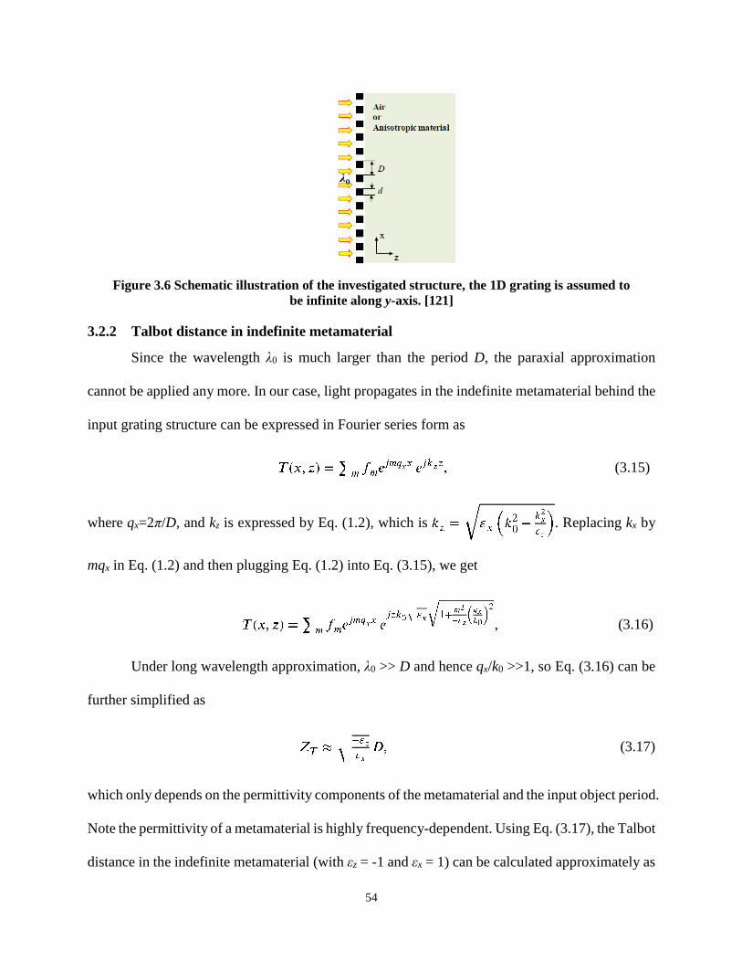
54
Figure 3.6 Schematic illustration of the investigated structure, the 1D grating is assumed to
be infinite along y-axis. [121]
3.2.2 Talbot distance in indefinite metamaterial
Since the wavelength λ0 is much larger than the period D, the paraxial approximation
cannot be applied any more. In our case, light propagates in the indefinite metamaterial behind the
input grating structure can be expressed in Fourier series form as
(3.15)
where qx=2π/D, and kz is expressed by Eq. (1.2), which is . Replacing kx by
mqx in Eq. (1.2) and then plugging Eq. (1.2) into Eq. (3.15), we get
(3.16)
Under long wavelength approximation, λ0 >> D and hence qx/k0 >>1, so Eq. (3.16) can be
further simplified as
(3.17)
which only depends on the permittivity components of the metamaterial and the input object period.
Note the permittivity of a metamaterial is highly frequency-dependent. Using Eq. (3.17), the Talbot
distance in the indefinite metamaterial (with εz = -1 and εx = 1) can be calculated approximately as

55
100nm, while the Talbot distance measured in the simulation is around 117nm. The difference
may come from that the ratio of the wavelength λ0 and the period D is only around 6.3 while Eq.
(3.17) is based on the condition that λ0>>D.
3.3 Results and Discussion
3.3.1 Talbot effect without paraxial approximation
Classical Talbot effect can only be observed under paraxial approximation, where the
incident wavelength should be much smaller than the period of the grating. Here, the focus is put
on the opposite condition, where the wavelength is larger than the period. For the 2D structure
shown in Fig. 3.7, the period of the grating D is 100nm, d is 50nm and the incident wavelength λ0
is 630nm. In a conventional material, the evanescent waves which carry the information about the
subwavelength features of the object will decay exponentially. Hence, if the period of the input
object is much smaller than the incident wavelength, no Talbot effect can be seen in the regular
material (as shown in Fig. 3.7(a), in the air). In contrast to the case in the air, self-imaging effect
can be achieved in an indefinite metamaterial, which is due to the evanescent waves being
converted into propagating waves and conveyed far away. This self-imaging effect observed in the
indefinite metamaterial when the period of the object much smaller than the incident wavelength
is defined as “super Talbot effect” in this paper. Figure 3.7(b) clearly shows the strong, periodic
magnetic field distribution pattern in the indefinite metamaterial (with εz = -1 and εx = 1) behind
the input grating. This effect is related to but also distinct from the plasmon Talbot effect reported
in recent work [141,142], where surface plasmon Talbot effect is observed on the surface of metal
and its resolution is still limited by the surface plasmon diffraction limit. In contrast, our super
Talbot effect is based on bulk plasmons without diffraction limit.
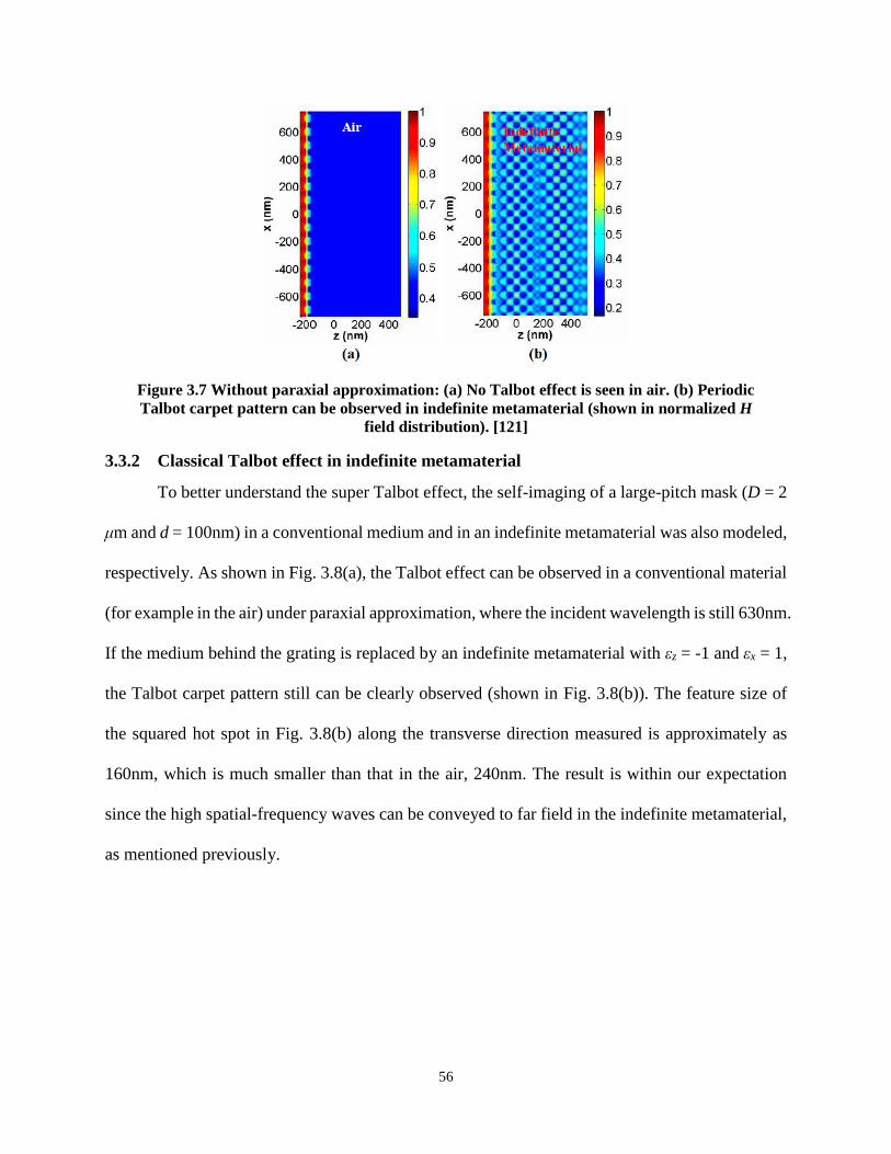
56
Figure 3.7 Without paraxial approximation: (a) No Talbot effect is seen in air. (b) Periodic
Talbot carpet pattern can be observed in indefinite metamaterial (shown in normalized H
field distribution). [121]
3.3.2 Classical Talbot effect in indefinite metamaterial
To better understand the super Talbot effect, the self-imaging of a large-pitch mask (D = 2
μm and d = 100nm) in a conventional medium and in an indefinite metamaterial was also modeled,
respectively. As shown in Fig. 3.8(a), the Talbot effect can be observed in a conventional material
(for example in the air) under paraxial approximation, where the incident wavelength is still 630nm.
If the medium behind the grating is replaced by an indefinite metamaterial with εz = -1 and εx = 1,
the Talbot carpet pattern still can be clearly observed (shown in Fig. 3.8(b)). The feature size of
the squared hot spot in Fig. 3.8(b) along the transverse direction measured is approximately as
160nm, which is much smaller than that in the air, 240nm. The result is within our expectation
since the high spatial-frequency waves can be conveyed to far field in the indefinite metamaterial,
as mentioned previously.

57
Figure 3.8 Talbot effect in (a) air, and (b) indefinite metamaterial. Both are shown in
normalized power distribution. [121]
3.3.3 Super Talbot effect in indefinite metamaterial
As mentioned previously in Section 1.2.3, indefinite metamaterial can be approximated by
a system of thin, alternating multilayer metal-insulator (MMI) stack. In this work, Ag and SiO2
were selected as the metal and insulator, respectively. The structure we investigated is similar as
shown in Fig. 3.4, where the material behind the grating was replaced by the MMI stack composed
of Ag and SiO2 thin layers and they were assumed to be infinite in y-axis. The alternating layers
were stacked in the x direction and each layer has a thickness of 5nm. In the simulations, periodic
boundary conditions were implemented for the boundaries parallel to the z-axis. The wavelength
of the incident TM-polarized plane wave λ0 = 630nm, the period of the grating D = 94nm and the
duty cycle = 50%. At the wavelength of interest, the permittivity of Ag is εAg = -15.69 + j1.06 and
that of SiO2 is εSiO2 = 2.12. As η = 1, from Eq. (1.3) the effective permittivity of the MMI stack is
calculated to be εz = -6.79 + j0.53 and εx = 4.9 + j0.05. Even the material loss is considered, the
super Talbot effect is still obvious as shown in Fig. 3.9(a). Figure 3.9(b) plots the cross-sectional
profile of the power in z-axis (where x = 52nm, the horizontal white solid line in the figure). Each
of the peaks numbered from 1 to 7 of the curve represents the location of one Talbot imaging plane
where the self-imaging phenomenon occurs. The intensity gradually decays due to the attenuation
of the MMI stack. The distance between the two adjacent peaks is the Talbot distance ZT, which is
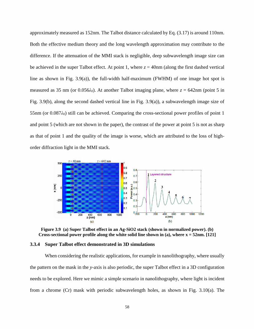
58
approximately measured as 152nm. The Talbot distance calculated by Eq. (3.17) is around 110nm.
Both the effective medium theory and the long wavelength approximation may contribute to the
difference. If the attenuation of the MMI stack is negligible, deep subwavelength image size can
be achieved in the super Talbot effect. At point 1, where z = 40nm (along the first dashed vertical
line as shown in Fig. 3.9(a)), the full-width half-maximum (FWHM) of one image hot spot is
measured as 35 nm (or 0.056λ0). At another Talbot imaging plane, where z = 642nm (point 5 in
Fig. 3.9(b), along the second dashed vertical line in Fig. 3.9(a)), a subwavelength image size of
55nm (or 0.087λ0) still can be achieved. Comparing the cross-sectional power profiles of point 1
and point 5 (which are not shown in the paper), the contrast of the power at point 5 is not as sharp
as that of point 1 and the quality of the image is worse, which are attributed to the loss of high-
order diffraction light in the MMI stack.
Figure 3.9 (a) Super Talbot effect in an Ag-SiO2 stack (shown in normalized power). (b)
Cross-sectional power profile along the white solid line shown in (a), where x = 52nm. [121]
3.3.4 Super Talbot effect demonstrated in 3D simulations
When considering the realistic applications, for example in nanolithography, where usually
the pattern on the mask in the y-axis is also periodic, the super Talbot effect in a 3D configuration
needs to be explored. Here we mimic a simple scenario in nanolithography, where light is incident
from a chrome (Cr) mask with periodic subwavelength holes, as shown in Fig. 3.10(a). The
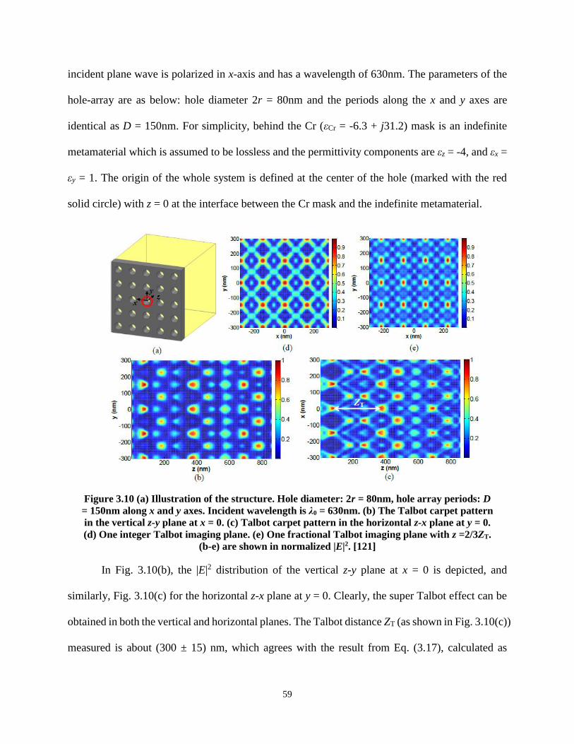
59
incident plane wave is polarized in x-axis and has a wavelength of 630nm. The parameters of the
hole-array are as below: hole diameter 2r = 80nm and the periods along the x and y axes are
identical as D = 150nm. For simplicity, behind the Cr (εCr = -6.3 + j31.2) mask is an indefinite
metamaterial which is assumed to be lossless and the permittivity components are εz = -4, and εx =
εy = 1. The origin of the whole system is defined at the center of the hole (marked with the red
solid circle) with z = 0 at the interface between the Cr mask and the indefinite metamaterial.
Figure 3.10 (a) Illustration of the structure. Hole diameter: 2r = 80nm, hole array periods: D
= 150nm along x and y axes. Incident wavelength is λ0 = 630nm. (b) The Talbot carpet pattern
in the vertical z-y plane at x = 0. (c) Talbot carpet pattern in the horizontal z-x plane at y = 0.
(d) One integer Talbot imaging plane. (e) One fractional Talbot imaging plane with z =2/3ZT.
(b-e) are shown in normalized |E|2. [121]
In Fig. 3.10(b), the |E|2 distribution of the vertical z-y plane at x = 0 is depicted, and
similarly, Fig. 3.10(c) for the horizontal z-x plane at y = 0. Clearly, the super Talbot effect can be
obtained in both the vertical and horizontal planes. The Talbot distance ZT (as shown in Fig. 3.10(c))
measured is about (300 ± 15) nm, which agrees with the result from Eq. (3.17), calculated as

60
300nm. The asymmetric pattern distributions as shown in Fig. 3.10(b) and 3.10(c) may be
attributed to the polarization dependent effect. Figure 3.10(d) shows the image in one of the Talbot
imaging planes (x-y plane, z = 365nm). The positions of the hot spots coincide with those of the
periodic holes on the Cr mask. The size of each hot spot (FWHM) is approximately 40nm-by-
40nm (or 0.0635λ0-by-0.0635λ0). Besides the integer self-imaging planes, we also observed some
fractional Talbot imaging planes which locate between two adjacent integer Talbot planes [143],
with z = p/qZT (p and q are prime integers). One representative fractional Talbot imaging plane
with z ≈ 2/3ZT was shown in Fig. 3.10(e). Comparing with the integer Talbot imaging plane [Fig.
3.10(d)], the image on the fractional Talbot imaging plane as shown in Fig. 3.10(e) has the same
spatial frequency but is shifted about 0.5 periods (75nm) along x-axis. The image size (FWHM)
of those hot spots is measured as 30nm-by-40nm (or 0.0476λ0-by-0.0635λ0).
Low loss 3D indefinite metamaterials may be constructed by an array of aligned metallic
nanowires (εm < 0) embedded in a dielectric host (εd > 0). The fabrication of the nanowire-based
metamaterial is based on a well-developed technique named “template synthetic method” [144-
147] and with the pores filled by metals.
3.4 Conclusions
In conclusion, we have shown that super Talbot effect can be observed in an indefinite
metamaterial without the paraxial approximation. A 2D indefinite metamaterial can be
approximated by a multilayer metal-insulator stack for super Talbot applications. As long as the
loss of the metamaterial is small enough, a deep subwavelength resolution (~0.087λ0) can be
achieved. Unlike the other plasmon Talbot effect discussed in Ref. [141,142], the super Talbot
effect in this work is based upon bulk plasmon without diffraction limit. The super Talbot effect

61
may find a variety of applications in the fields as nanolithography and optical storage. In particular,
3D photonic crystals may be fabricated based the super 3D self-imaging phenomenon [148].

62
4 NANOPLASMONIC OPTICAL SWITCH BASED ON
GA-SI3N4-GA WAVEGUIDE
In the previous two chapters, we introduced two different types of metamaterials --
designer surface plasmonic (DSP) waveguides [85] with periodic patterns on metal surface and an
indefinite metamaterial consisting of alternative thin metal and dielectric layers [121], where in
both cases the novel properties were achieved by man-made structures. In this chapter, we will see
that a natural material – gallium (Ga), can also be treated as metamaterial, where the refractive
index of gallium changes via the phase transitions of the material itself [149]. A numerical study
of optical switch based on a metal-insulator-metal plasmonic waveguide with Si3N4 core
sandwiched between two gallium (Ga) metal layers, is present [150]. Combining the unique
structural phase transition property of gallium, within a total length of 400nm, an extinction ratio
as high as 7.68 dB can be achieved in the proposed nanoplasmonic structure [150].
4.1 Introduction
Silicon is a prevalent, also a favorite choice in photonics, and silicon-based photonic
components ranging from passive devices to active devices (like modulators, detectors, and light
amplifiers) have been intensively investigated and developed [151-153]. On the other hand, silicon
has the drawbacks of relatively low electro-optic coefficient and low light emission efficiency,
which make silicon not a suitable for dense circuit component integration. A promising solution
may be found in surface plasmon polaritons (SPPs), i.e. surface electromagnetic excitations
coupled with collective electrons, which have intrigued considerable interest. Since SPPs exhibit
extremely small guiding wavelengths and high field intensities along dielectric-metal interfaces,
optical confinement can be scaled to deep subwavelength dimensions in plasmonic devices.

63
In recent years, considerable interest arises in the nonlinear effect enhancement by
structural phase transitions in polyvalent metals, for example, Ga, which has already shown to
enable all optical switching at mill watt power levels in thin films [154] and nanoparticles [155],
as well as promises a new type of photodetector [156]. Gallium is a material known for its
polymorphism [157]. The stable “ground-state” phase, α-gallium, is a highly anisotropic metal
because molecular and metallic properties may coexist – some inter-atomic bonds are strong
covalent bonds, forming well-defined Ga2 molecules, and the rest are metallic bonds [149]. The
structure is highly anisotropic, with much better thermal and electrical conductivity in the “metallic
planes” than along the covalent bonds. The phase transitions between α-gallium and metallic
gallium will occur when the temperature is close to the melting temperature of α-gallium, which
is very low as 29.8ºC. The switching may be achieved by external optical excitation or just simply
changing the temperature of the metal with the switching time approximately in the picosecond-
microsecond range [158]. The significant difference in the optical properties of α-phase and
metallic phase makes gallium a very suitable material for plasmonic modulators and switches,
when α-gallium is near its melting point. However, gallium also presents another means to achieve
metallic phase, by a non-thermal transition [158,159]. With high intensity femtosecond optical
excitation, the molecular character of the α-gallium structure results in highly localized excitation
of the dimers, due to the very fast localization of the photo-generated electron-hole pairs on the
dimers. Therefore, light absorption can excite a dimer from the bonding to the anti-bonding state.
Consequently, the α-gallium structure transits to a new configuration, as shown in Fig. 4.1, without
near the melting temperature [149]. This process is called light-induced surface-assisted
metallization [149].

64
Figure 4.1 Surface light-induced metallization at a gallium-silica interface, at a wavelength of
1.55μm. [149]
In 2004, Krasavin and Zheludev proposed an active Au/Ga waveguide [154], which
contains a 2.5μm long gallium switching layer, as illustrated in Fig. 4.2. The mechanism of the
modulation is from the great different optical properties of the α-gallium and liquid gallium, in
terms of the dielectric constants, |εliquid - εα| ~ 180 at a wavelength of 1.55μm [154]. For a section
of gallium waveguide 2.5μm-by-2.5μm the optical energy required for high-contrast switching will
be on the order of 10 pJ. The intrinsic switch-on time was found to be 2-4 ps [160], which was
measured on a gallium-quartz interface. The SPP switch-on time will be expected to be also on the
scale of a few ps, while the switch-off to be in μs-ns time scale [158].

65
Figure 4.2 A SPP-based gold-on-quartz waveguide containing a gallium switching section,
where gallium is at the bottom of the quartz substrate, shown in the magnitude of the
magnetic field. [154]
4.2 Design and Modeling
Based on the previous work [154], in this work [150] the unique phase transition property
of gallium is employed and the focus is put on the signal light transmission through a simple Ga-
Si3N4-Ga waveguide. Finite-difference time-domain (FDTD) method [108,109] is used to
investigate the switching properties of the plasmonic waveguide. In the FDTD simulations, the
experimental data for the frequency-dependent dielectric constants of Ga is directly used [161,162],
including both the real and imaginary parts for the three main crystalline axes (a-axis, b-axis, and
c-axis) of α-gallium and the metallic gallium. At a wavelength of 1.55μm, the dielectric constants
of different phase of gallium are: εmetallic=-132.84+j134.77, εα_a-axis=-3.61+j23.79, εα_b-axis=-
36.43+j21.79, and εα_c-axis =2.83+j21.62. The simulated structure is created as a simple coupler by
placing a Ga-Si3N4-Ga plasmonic waveguide embedded between two identical dielectric (silicon)
waveguides, as shown in Fig. 4.3(a). The silicon waveguides and the Ga-Si3N4-Ga waveguide are
aligned along the light propagation direction. The two silicon waveguides are used to couple
optical signals into and out of the Ga-Si3N4-Ga waveguide, respectively. Recent work shows that
high efficiency photonic-plasmonic-photonic coupling can be achieved through this configuration
[163]. In order to calculate the power transmission of the Ga-Si3N4-Ga waveguide, a fundamental

66
TM mode in the input silicon waveguide is excited by a mode source. The power fluxes are
measured in both the input and output silicon waveguides. Since the center of attention describes
the switching characteristics of the plasmonic waveguide, the parameter optimization of the whole
structure to achieve high extinction ratios, as well as waveguide transmission, will be discussed
later in this chapter. The geometrical parameters of the silicon waveguides are temporarily put as:
the width of the silicon waveguides, wd = 400nm, the length of the Ga-Si3N4-Ga waveguide, lp =
400nm, and the width of dielectric core, wp = 60nm. Perfectly matched layers are used at all the
boundaries of the simulation area to minimize the unnecessary reflection [164]. The spatial and
temporal steps are set as Δx = Δy = 2nm and Δt = Δx/2c [165] respectively, to ensure accurate
results in the FDTD simulations and c is the speed of light in free space.
Figure 4.3 (a) A Ga-Si3N4-Ga plasmonic waveguide embedded between two silicon dielectric
waveguides. (b) Dielectric gaps are introduced at both ends of the plasmonic waveguide. [150]
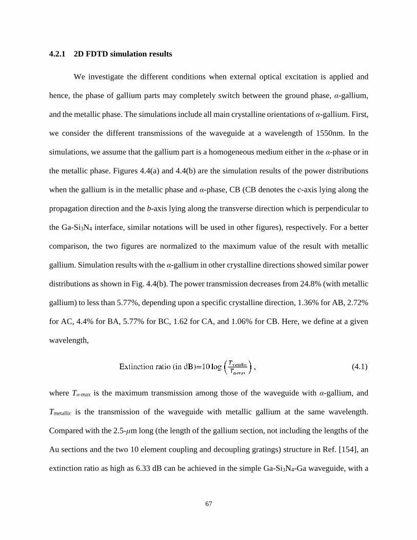
67
4.2.1 2D FDTD simulation results
We investigate the different conditions when external optical excitation is applied and
hence, the phase of gallium parts may completely switch between the ground phase, α-gallium,
and the metallic phase. The simulations include all main crystalline orientations of α-gallium. First,
we consider the different transmissions of the waveguide at a wavelength of 1550nm. In the
simulations, we assume that the gallium part is a homogeneous medium either in the α-phase or in
the metallic phase. Figures 4.4(a) and 4.4(b) are the simulation results of the power distributions
when the gallium is in the metallic phase and α-phase, CB (CB denotes the c-axis lying along the
propagation direction and the b-axis lying along the transverse direction which is perpendicular to
the Ga-Si3N4 interface, similar notations will be used in other figures), respectively. For a better
comparison, the two figures are normalized to the maximum value of the result with metallic
gallium. Simulation results with the α-gallium in other crystalline directions showed similar power
distributions as shown in Fig. 4.4(b). The power transmission decreases from 24.8% (with metallic
gallium) to less than 5.77%, depending upon a specific crystalline direction, 1.36% for AB, 2.72%
for AC, 4.4% for BA, 5.77% for BC, 1.62 for CA, and 1.06% for CB. Here, we define at a given
wavelength,
(4.1)
where Tα-max is the maximum transmission among those of the waveguide with α-gallium, and
Tmetallic is the transmission of the waveguide with metallic gallium at the same wavelength.
Compared with the 2.5-μm long (the length of the gallium section, not including the lengths of the
Au sections and the two 10 element coupling and decoupling gratings) structure in Ref. [154], an
extinction ratio as high as 6.33 dB can be achieved in the simple Ga-Si3N4-Ga waveguide, with a

68
total length of only 400nm. This result is noticeable since the optical switch has been considered
as a part of the integrated circuit, and the embedded structure is ready for fabrication. The detailed
fabrication processes will be discussed in Section 4.3.
Figure 4.4 (a) Simulation result of field distribution with metallic gallium. (b) Simulation
result of field distribution with α-gallium, CB [150]. Both plots are normalized with the result
with metallic gallium.
To further investigate the performance of the modulator, we varied the working
wavelengths of the optical switch from 1000 to 2000nm in the simulations. Figure 4.5 shows the
transmissions at different wavelengths of incident light for the same structure. The most important
information obtained from the simulation results is that the structural phase of the gallium is the
main factor to determine the transmission of the Ga-Si3N4-Ga waveguide. From Fig. 4.5, we find
that as the wavelength increases, the transmission levels for all the cases increase, except for the
transmission of the waveguide with metallic gallium decreases at a very narrow wavelength range
(1000 to 1070nm). We also note that an extinction ratio over 3 dB (not shown in Fig. 4.5) can be
achieved at wavelengths approximately from 1160 to 2000nm. The reason can be attributed to the
following: when the structural phase of gallium changes, the changed refractive index of gallium
will cause the propagation loss as well as the impedance change. By carefully examining Fig. 4.5,
(a) (b)
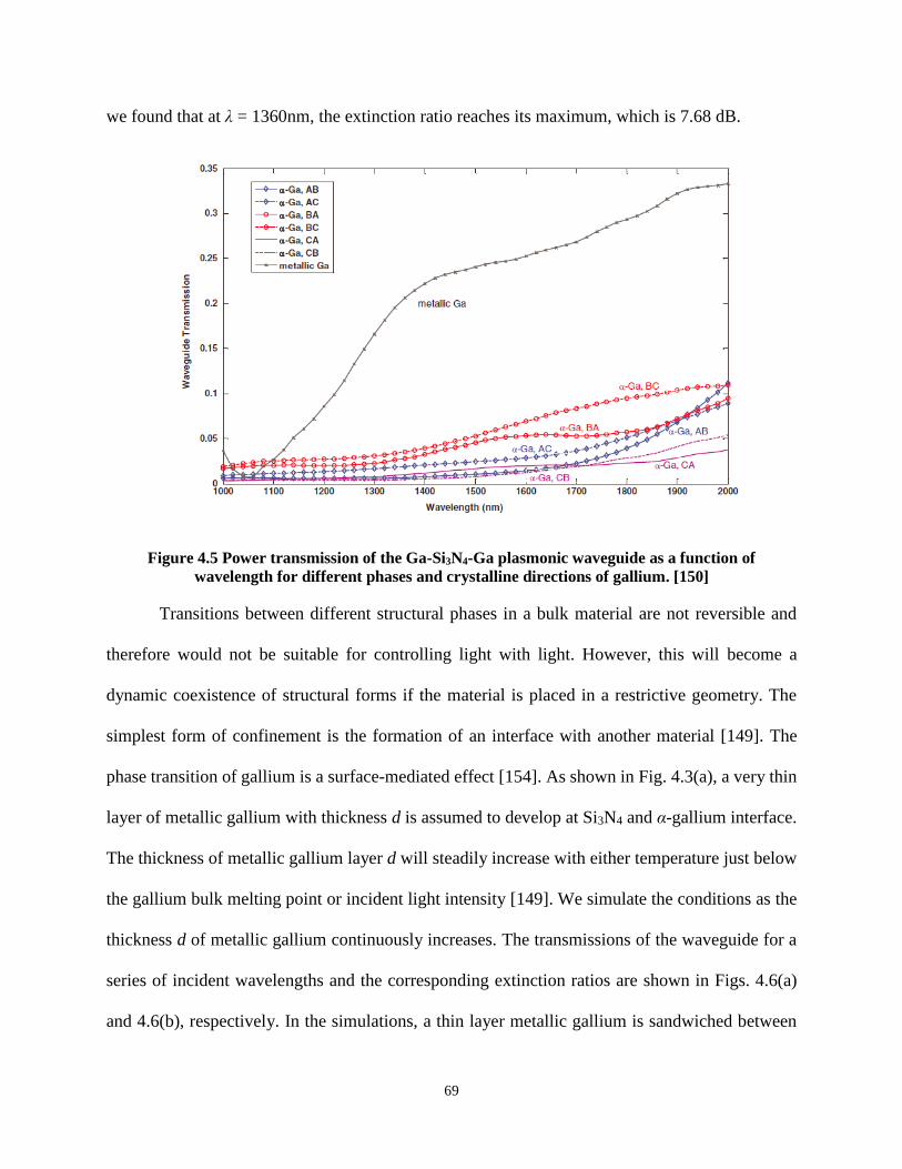
69
we found that at λ = 1360nm, the extinction ratio reaches its maximum, which is 7.68 dB.
Figure 4.5 Power transmission of the Ga-Si3N4-Ga plasmonic waveguide as a function of
wavelength for different phases and crystalline directions of gallium. [150]
Transitions between different structural phases in a bulk material are not reversible and
therefore would not be suitable for controlling light with light. However, this will become a
dynamic coexistence of structural forms if the material is placed in a restrictive geometry. The
simplest form of confinement is the formation of an interface with another material [149]. The
phase transition of gallium is a surface-mediated effect [154]. As shown in Fig. 4.3(a), a very thin
layer of metallic gallium with thickness d is assumed to develop at Si3N4 and α-gallium interface.
The thickness of metallic gallium layer d will steadily increase with either temperature just below
the gallium bulk melting point or incident light intensity [149]. We simulate the conditions as the
thickness d of metallic gallium continuously increases. The transmissions of the waveguide for a
series of incident wavelengths and the corresponding extinction ratios are shown in Figs. 4.6(a)
and 4.6(b), respectively. In the simulations, a thin layer metallic gallium is sandwiched between

70
Si3N4 and α-gallium, CB. The simulated structure and main geometric parameters are kept the
same as the previous simulations. It is clearly seen that with the presence of tens of nanometers
thick metallic gallium, the transmissions of the waveguide, as well as the extinction ratios, increase
rapidly. This may be due to that only the metal in the vicinity of the metal-dielectric interface will
be involved in the switching processes, since the field decays exponentially inside the metal at the
interface. As shown in Fig. 4.6(b), at λ = 1550nm, with a 40-nm thick metallic gallium layer, the
extinction ratio reaches around 9.98 dB and the transmission increases to 10 times of its original
value [see Fig. 4.6(a)]. The plasmonic waveguide with metallic gallium represents an “on” state
while with α-gallium represents an “off” state. The transmission of the waveguide with metallic
gallium can be improved by choosing the optimal geometric parameters of the waveguide or
simply introducing dielectric gaps to the structure, as shown in Fig. 4.3(b). Those gaps may
function like “funnels” to gather more SPPs to the dielectric core of the waveguide [165]. With
two 40-nm wide gaps placed at both ends of the plasmonic waveguide, at an incident wavelength
of 1550nm, the transmission of the waveguide with metallic gallium is improved to 30.3%, while
the extinction ratio is approximate 7.05 dB. Other parameters (e.g., the width of Si3N4 core, wp),
can also be optimized to increase the power transmission. From simulation results, with increased
core thickness wp, the transmission of the waveguide will increase as well. For example, when wp
= 90nm, transmission of the waveguide with metallic gallium increases to 39.7% at λ = 1550nm.
The whole structure exhibits Fabry–Pérot effect as the length of the plasmonic waveguide changes
[163], when the length of the Ga-Si3N4-Ga waveguide is 140nm, transmission with metallic
gallium is around 40.7%, and the extinction ratio is approximately 4.25 dB.
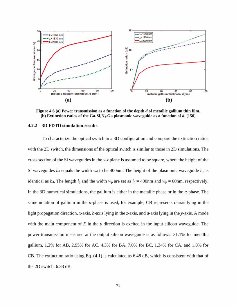
71
Figure 4.6 (a) Power transmission as a function of the depth d of metallic gallium thin film.
(b) Extinction ratios of the Ga-Si3N4-Ga plasmonic waveguide as a function of d. [150]
4.2.2 3D FDTD simulation results
To characterize the optical switch in a 3D configuration and compare the extinction ratios
with the 2D switch, the dimensions of the optical switch is similar to those in 2D simulations. The
cross section of the Si waveguides in the y-z plane is assumed to be square, where the height of the
Si waveguides hd equals the width wd to be 400nm. The height of the plasmonic waveguide hp is
identical as hd. The length lp and the width wp are set as lp = 400nm and wp = 60nm, respectively.
In the 3D numerical simulations, the gallium is either in the metallic phase or in the α-phase. The
same notation of gallium in the α-phase is used, for example, CB represents c-axis lying in the
light propagation direction, x-axis, b-axis lying in the z-axis, and a-axis lying in the y-axis. A mode
with the main component of E in the y direction is excited in the input silicon waveguide. The
power transmission measured at the output silicon waveguide is as follows: 31.1% for metallic
gallium, 1.2% for AB, 2.95% for AC, 4.3% for BA, 7.0% for BC, 1.34% for CA, and 1.0% for
CB. The extinction ratio using Eq. (4.1) is calculated as 6.48 dB, which is consistent with that of
the 2D switch, 6.33 dB.
(a) (b)

72
4.3 Proposed Fabrication Steps
Figure 4.7 (a) Starting the fabrication process on an SOI wafer. (b) Defining the input and
output silicon waveguide. (c) Deposition of Si3N4 film as the core of the plasmonic waveguide.
(d) Deposition of gallium film. [150]
Here, a possible 3D implementation of the optical switch is proposed. Figures 4.7(a) –4.7(d)
illustrates the main fabrication steps of the optical switch. First, the input and output silicon
waveguides will be fabricated on a silicon-on-insulator (SOI) wafer. In the second step, the
dielectric core of the plasmonic waveguide, silicon nitride, will be deposited between the two
silicon waveguides by a method named hot-wires chemical vapor deposition [167]. With NH3/SiH4
ratios between 40 and 70, and at low substrate temperature of 100ºC or 250ºC, dense films (2.56
to 2.74 g/cm3) and refractive index between 1.93 and 2.08 can be obtained [167]. The following
lithography and etch steps will pattern the dielectric core. Good alignment is required to make the
dielectric core be in alignment with the input/output silicon waveguides in the y-axis. In the third
step, a high quality gallium film will be deposited on the substrate from Ga targets using a Q-
switched mode-locked Nd:YAG laser (λ=1.064 μm; τFWHM =60 ps) [168]. It has been reported
that gallium nanoparticles with a relatively narrow size could be formed on the substrate if it was
illuminated by very low intensity laser light [169,170]. The gallium film will re-solidify to α-phase
after the melting process [168].
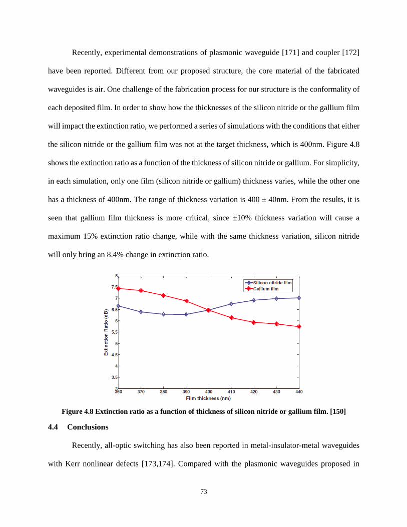
73
Recently, experimental demonstrations of plasmonic waveguide [171] and coupler [172]
have been reported. Different from our proposed structure, the core material of the fabricated
waveguides is air. One challenge of the fabrication process for our structure is the conformality of
each deposited film. In order to show how the thicknesses of the silicon nitride or the gallium film
will impact the extinction ratio, we performed a series of simulations with the conditions that either
the silicon nitride or the gallium film was not at the target thickness, which is 400nm. Figure 4.8
shows the extinction ratio as a function of the thickness of silicon nitride or gallium. For simplicity,
in each simulation, only one film (silicon nitride or gallium) thickness varies, while the other one
has a thickness of 400nm. The range of thickness variation is 400 ± 40nm. From the results, it is
seen that gallium film thickness is more critical, since ±10% thickness variation will cause a
maximum 15% extinction ratio change, while with the same thickness variation, silicon nitride
will only bring an 8.4% change in extinction ratio.
Figure 4.8 Extinction ratio as a function of thickness of silicon nitride or gallium film. [150]
4.4 Conclusions
Recently, all-optic switching has also been reported in metal-insulator-metal waveguides
with Kerr nonlinear defects [173,174]. Compared with the plasmonic waveguides proposed in

74
those papers, the switching mechanism of our Ga-Si3N4-Ga waveguide mainly depends on the
waveguide material (gallium) property, not by introducing an additional nonlinear medium. Hence,
our proposed structure is much simpler and easier to fabricate.
To summarize, in this chapter the potential switching properties of a simple Ga-Si3N4-Ga
plasmonic waveguide is investigated. With a length of only 400nm, an extinction ratio as 7.68 dB
can be achieved in the proposed structure. Since the phase transition of gallium is a surface-
mediated effect, we also show that with tens of nanometers thick metallic gallium sandwiched
between Si3N4 and α-gallium, the power transmission level will increase greatly. Further study on
the parameter optimization confirms that the transmission of the waveguide can be improved to
40.7%, while the extinction ratio is still kept over 4.25 dB.

75
5 ITO-BASED MULTILAYER ELECTRO-OPTICAL
MODULATOR
Gallium is not the only naturally existing metamaterial. From Chapter 5 to Chapter 8, we
will introduce another two natural metamaterials – ITO and graphene, and explore their
applications in ultra-compact modulators.
In this chapter, we investigated an active plasmonic metamaterial – ITO and its application
in electro-optical modulators, where the structures are planar multilayer structure. Here we also
use a new material named electrolyte gel to enhance the modulation effect. When applying external
voltages on these multilayer structures, electric double layers are formed at the interfaces of ITO
and electrolyte gel, which can attract more electrons or holes in ITO. Two different structures:
ITO/electrolyte gel/doped-Si and ITO/electrolyte gel/ITO, are investigated. Based on attenuated
total reflection (ATR) measurement results, modulation depth up to 38.8% can be achieved.
Preliminary result is present for the real time response of an ITO/electrolyte gel/doped-Si
modulator.
5.1 Introduction
Conventional photonic elements have physical dimensions on the order of the wavelength
of light, due to the diffraction limits of light in those devices. Hence, the difference in the physical
sizes between the nanometer-scale electronic devices and the micrometer-scale photonic devices
leads to the incompatibility between these two types of devices. Surface plasmon polaritons (SPPs)
combines the high bandwidth offered by photonics and the nanometer-scale device size offered by
nano-electronics by coupling a photon’s energy with a free-electron gas, creating a subwavelength,

76
oscillating mode at the interface of dielectric and metal. Plasmonics and metamaterials are driving
the development of novel devices with unprecedented functionalities, such as subwavelength
waveguides [175-177], superlenses [4,5,178], optical invisibility cloaks [179-181], and planar
magnifying hyperlens and light concentrators [182-184]. Since the plasmon phenomenon in optical
and telecommunication frequencies typically originates from the collective oscillations of free
charges in a material, plasmonic devices generally require metallic components. The abundant free
electrons provide the negative real permittivity, which is an essential property of plasmonic
material. One important challenge in these fields is the high loss caused by the metallic components
in the devices, especially in the visible and ultra-violet (UV) spectrum regime. The high loss is a
major obstacle in the design of efficient devices, seriously limiting the feasibility of many
plasmonic applications. In order to compensate the high loss, optical gain materials are combined
with metallic structures [185-187]. However, even the best gain materials available are barely
enough to compensate the losses in metals. Therefore, alternative plasmonic materials with lower
losses are desired to develop robust plasmonic devices and overcome the major bottleneck.
Conventionally, semiconductors are regarded as dielectric materials for frequencies above
several hundred THz. However, semiconductors can exhibit a negative real permittivity in this
spectrum regime under certain conditions [103,188,189]. Due to the flexibility in tuning the carrier
concentration, semiconductors are potential alternative plasmonic materials. Indium-tin-oxide
(ITO), a representative of TCOs, has been shown to be a potential plasmonic material in the near-
infrared (NIR) region [190-192]. ITO is transparent degenerately doped semiconductor, containing
90%wt indium oxide (In2O3) and 10%wt tin oxide (SnO2), which is widely used as transparent
electrodes in solar cells and displays [103,193,194].The exploration of TCOs as the plasmonic
metamaterial for near-infrared (NIR) applications can be traced back to decades ago [190,192,195].

77
Comparative studies can be found in Refs. [25,196]. The carrier concentration in ITO is in the
range of 1019~1021/cm3, which can be controlled by manipulating the concentration of oxygen
vacancies and interstitial metal dopants. The high carrier concentration enables guiding surface
mode at the interface of ITO and dielectric materials, for example air, which has a great potential
in the applications of electro-optic (EO) modulators [24,107].
5.2 Transfer Matrix Method (TMM)
The transfer matrix method [197-199] in optics is a powerful numerical method used to
analyze the propagation of the electromagnetic waves through a layered medium. According to
Maxwell’s equations, there are simple continuity conditions for the electric/magnetic field across
boundaries from one medium to the next medium. If the field is known at the beginning of a layer,
the field at the end of the layer can be derived from a simple matrix operation. Therefore, a stack
consisted of multiple layers can be represented as a system of matrix, which is a product of the
individual layer matrices. By converting the system matrix back into reflection and transmission
coefficients is the final step of this method.
5.2.1 Single boundary
Considering a wave transmits through a planar boundary between two materials with
indexes n0 and n1 as illustrated in Fig. 5. 1, we have according to Snell’s law.
The transfer matrix M01 can be expressed as
, (5.1)
where , , for TE mode, and , ,
for TM mode.

78
Figure 5.1 Oblique incidence.
5.2.2 Propagation in a multilayer stack
Figure 5.2 shows an incoming light beam transmitted through a planar multiple layer stack
from medium 1 to medium (i-1), where media 0 and i are the input and output media, respectively.
Figure 5.2 Illustration of a planar multilayer stack, incoming light comes from medium 0 and
leaves the stack from medium (i-1).
As the light beam transmits from medium 0 to medium 1 with an oblique angle, at the
boundary, the transmission matrix M01 can be expressed as Eq. (5.1). When the light transmits
through medium 1 to medium 2 and propagates in medium 2, the transmission matrix will be added
one propagation term and expressed as
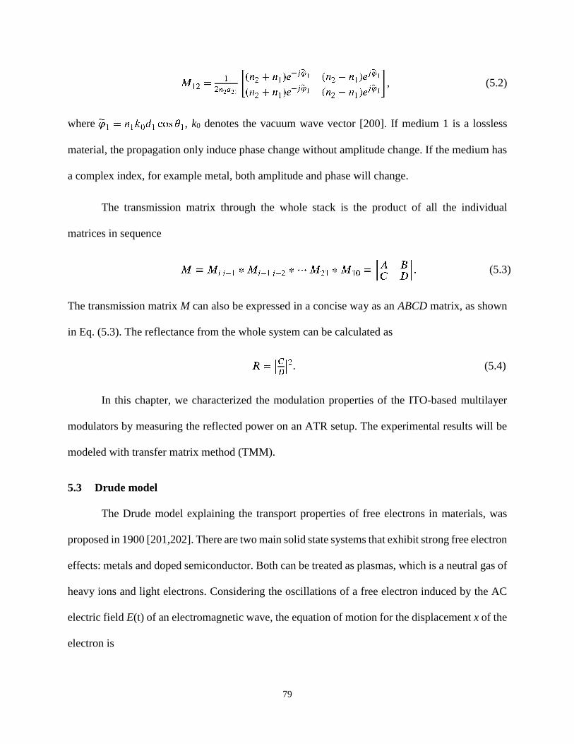
79
, (5.2)
where , k0 denotes the vacuum wave vector [200]. If medium 1 is a lossless
material, the propagation only induce phase change without amplitude change. If the medium has
a complex index, for example metal, both amplitude and phase will change.
The transmission matrix through the whole stack is the product of all the individual
matrices in sequence
(5.3)
The transmission matrix M can also be expressed in a concise way as an ABCD matrix, as shown
in Eq. (5.3). The reflectance from the whole system can be calculated as
. (5.4)
In this chapter, we characterized the modulation properties of the ITO-based multilayer
modulators by measuring the reflected power on an ATR setup. The experimental results will be
modeled with transfer matrix method (TMM).
5.3 Drude model
The Drude model explaining the transport properties of free electrons in materials, was
proposed in 1900 [201,202]. There are two main solid state systems that exhibit strong free electron
effects: metals and doped semiconductor. Both can be treated as plasmas, which is a neutral gas of
heavy ions and light electrons. Considering the oscillations of a free electron induced by the AC
electric field E(t) of an electromagnetic wave, the equation of motion for the displacement x of the
electron is

80
(5.5)
where ω is the frequency of the light, and E0 is its amplitude. The acceleration of the electron is
represented by the first term, while the second is the frictional damping force of the material. The
term on the right hand side is the driving force exerted by the light.
By substituting into Eq. (5.5), we can obtain . The
polarization P of the gas is equal to –Nex, where N is the number of electron per unit volume.
Recalling the electric displacement field D, which is defined as 𝜀 𝜀 . Therefore,
D can be written as
. (5.6)
Hence, we can get
(5.7)
This equation can be written in a more concise form as
(5.8)
where
(5.9)
is known as the plasma frequency, while e is the unit electric charge, ε0 the free space permittivity,
and m0 the electron mass. The plasma frequency ωp corresponds to the natural resonant frequency
of the free carrier gas.

81
The free electron model presented above can be applied to doped semiconductors if two
appropriate modifications [203]. Firstly, the fact that the electrons and holes are moving in the
conduction or valence band of a semiconductor needs to be considered. In this scenario, we can
assume that those carriers behave as particles with an effective mass m* rather than the free
electron mass m0. Secondly, there are other mechanisms that may contribute to the dielectric
constant as well as the free carrier effects. The main extra part is the contribution to the polarization
due to the optical response of the bound electrons. Therefore, Eq. (5.6) can be rewritten in the
following form when the two modifications are considered
(5.10)
The effective mass m* accounts for the band structure of the semiconductor, ε∞ is the high
frequency dielectric constant, and carrier density N in this equation is the density of free electrons
or holes generated by the doping process. From Eq. (5.10) we can write the frequency dependence
of the dielectric constant as
(5.11)
where is the plasma frequency. Since the carrier density is much smaller than that in
metals, the plasma frequency may occur in the infrared spectral range.
In this chapter, we will use Eq. (5.11) to model the optical properties of ITO, where the
ITO is treated as doped-semiconductor.

82
5.4 Optical property of ITO
Figure 5.3 ATR setup in Kretschmann configuration.
An attenuated total reflection (ATR) setup was built in the Kretschmann configuration
[204], as illustrated in Fig. 5.3. A collimated laser beam propagates through a broadband polarizer
(P1), and the output is either s- or p- polarized light, and is then split into two by a beam splitter
(BS). One beam is used for collecting source power fluctuation and fed into a Ge photodiode (PD2);
another is incident at the angle θ into a BK7 glass hemi-cylindrical (Ø100mm obtained from
Rocoptonics) lens, which functions as a coupling prism in this setup. The reflected light is then
collected by another Ge photodiode (PD1). The reflectance, R, is well measured by the power ratio
between PD1 and PD2, even there is power fluctuation in the laser source. The rotation of the
prism (together with the multilayer ITO modulator) and PD1 is in a θ-2θ configuration, which is
precisely controlled by two motorized rotation stages. The increment of θ is set as 0.25º.The
measurement result is recorded by a LabView program, thus, the reflectance R as a function of θ
can be plotted.
The measured reflectance of the ITO on corning glass slide is numerically fitted by
calculating the reflectance through the multilayer structure based on the transfer matrix method
(TMM) [197-199]. In order to avoid the thin air gap between the sample and the BK7 prism, a
PD1PD2Laser
BS
P1
R
θ
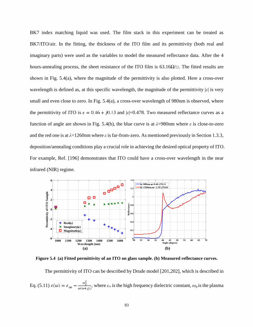
83
BK7 index matching liquid was used. The film stack in this experiment can be treated as
BK7/ITO/air. In the fitting, the thickness of the ITO film and its permittivity (both real and
imaginary parts) were used as the variables to model the measured reflectance data. After the 4
hours-annealing process, the sheet resistance of the ITO film is 63.16Ω/. The fitted results are
shown in Fig. 5.4(a), where the magnitude of the permittivity is also plotted. Here a cross-over
wavelength is defined as, at this specific wavelength, the magnitude of the permittivity |ε| is very
small and even close to zero. In Fig. 5.4(a), a cross-over wavelength of 980nm is observed, where
the permittivity of ITO is and |ε|=0.478. Two measured reflectance curves as a
function of angle are shown in Fig. 5.4(b), the blue curve is at λ=980nm where ε is close-to-zero
and the red one is at λ=1260nm where ε is far-from-zero. As mentioned previously in Section 1.3.3,
deposition/annealing conditions play a crucial role in achieving the desired optical property of ITO.
For example, Ref. [196] demonstrates that ITO could have a cross-over wavelength in the near
infrared (NIR) regime.
Figure 5.4 (a) Fitted permittivity of an ITO on glass sample. (b) Measured reflectance curves.
The permittivity of ITO can be described by Drude model [201,202], which is described in
Eq. (5.11) 𝜔 where ε∞ is the high frequency dielectric constant, ωp is the plasma
1000 1100 1200 1300 1400 1500 1600-6
-4
-2
0
2
4
6
Wavelength (nm)
Perm
itti
vit
y o
f IT
O S
am
ple
Real()
Imaginary()
Magnitude()
20 25 30 35 40 45 50 55 60 65 700
0.2
0.4
0.6
0.8
1
1.2
1.4
Angle (degree)
Refl
ecta
nce
=980nm, =0.46+j*0.13
=1260nm, =-1.19+j*0.64
(a) (b)

84
frequency, and γ is the electron damping factor. Hence, the carrier concentration in ITO can be
determined by
(5.12)
where ωp is the plasma frequency, and m* is the effective mass of electron. Assuming ε∞= 4 [196],
the carrier concentration is estimated as N=4.12E+21/cm3 at wavelength of 980nm.
5.5 ITO-based multilayer modulators
5.5.1 Fabrication of multilayer structure
Figure 5.5 Illustration of ITO-based multilayer modulator: (a) ITO/gel/doped-Si, and (b)
ITO/gel/ITO. (c) Commercial Electrolyte gel.
Figure 5.5(a) and (b) illustrate two different types of ITO-based multilayer modulators,
which are similar as that of metal-oxide-semiconductor (MOS). Here, an electrolyte gel is used to
replace the sandwiched oxide material and form simple planar multilayer structure. Electrolyte has
been used as gate insulators in organic field-effect transistors in 2005 by Nilsson et. al. [206]. The
interface between a metal (or heavily-doped semiconductor) and electrolyte is of interest in most
electrolyte applications, where two parallel layers of positive and negative charges called an
electric double layer (EDL) are formed. Another advantage of using electrolyte as the gating
SiO2
ITO
Electrolyte Gel
Highly doped Si
(a)
(b) (c)

85
material is, the device behavior can be conveniently controlled by varying the concentration of
chemical compounds in the electrolyte [207,208]. In our experiments, a commercially available
electrolyte Redux® Gel is used to fabricate the ITO-based multilayer modulators. Sodium chloride
(NaCl) is the main chemical compound in the electrolyte gel that makes it highly conductive. The
fabrication of the modulators starts from ITO film deposition on a transparent glass slide, as
described in Section 5.4. After applying a thin layer of electrolyte gel on the surface of ITO film,
either a heavily doped (resistivity as low as 0.001-0.002Ω·cm) silicon chip or another identical
ITO sample with the ITO side facing the electrolyte gel is tightly pushed toward the substrate ITO
to form the multilayer modulator, as shown in Fig. 5.5(a) and (b), respectively. With this
fabrication method, the thickness of the sandwiched electrolyte gel is usually 4-6μm, which is
determined by the numerical fitting.
5.5.2 Experimental demonstration of modulation effect
An ATR setup as illustrated in Fig. 5.3 was used to test the modulation performance of the
two types of ITO-based modulators. During the experiment, the ITO-based modulators were
mounted on the back of the hemi-cylindrical BK7 prism. To avoid a thin air gap between the prism
and the modulator, a BK7 index matching liquid is applied between them. In all the experiments,
the reflectance of the modulators was measured in a sequence of: (1) without externally applied
voltage, (2) with an externally applied voltage VP, and (3) with an externally applied voltage which
has reversed polarity but the same magnitude. We firstly focused on a simple structure, as shown
in Fig. 5.6(a), which includes only one active ITO layer. The measured reflectance of the
modulator with different applied voltages, as a function of θ with a p-polarized incident light beam
at λ = 1520nm is shown in Fig. 5.6. With an applied voltage, an EDL is formed at the interface of
the electrolyte gel and the ITO. Here we assumed there is a 5nm-thick [24] depletion layer (with

86
positive voltage VP = 10 V, illustrated in Fig. 5.6), or a 5nm-thick accumulation layer (with
negative voltage -VP=-10V) formed in ITO at the interface. The modulation depth, M(θ), as a
function of angle θ at a given wavelength can be defined as:
(5.13)
where R0 is the experimentally measured reflectance without applied voltage, is the
magnitude of the difference of the two reflectance with applied voltages. From Fig. 5.5, the
modulation depth at a specific angle of θ=70º can be calculated as M(70º)=20.7%. We attribute
the modulation to the change of the free carrier concentration in either the 5nm-thick depletion
layer or the accumulation layer in ITO at the interface, which is assisted by the redistribution of
the ions in electrolyte gel induced by the applied voltage. The charge distribution at the interface
and electric potential (V) at a stable status with the applied voltage is schematic illustrated in Fig.
5.6.
Figure 5.6 Normalized reflectance as a function of angle for the ITO/electrolyte gel/heavily-
doped Si modulator with different applied voltages. Inset: illustration of the modulator with
applied voltage.
20 30 40 50 60 700
0.2
0.4
0.6
0.8
1
1(degree)
Refl
ecta
nce
No voltage
VP=+10V
VP=-10V
Vp+ + + + + + + + +
Electrolyte gel
ITO
|V|
VP=10V

87
The measured reflectance of the ITO modulator is numerically fitted by calculating the
reflectance through the multilayer structure based on the transfer matrix method (TMM) [197-199].
In this experiment, the film stack can be treated as BK7/ITO/electrolyte gel/heavily-doped Si. In
order to simplify the fitting, we used the permittivity of the 5nm depletion layer or accumulation
layer in ITO (both real and imaginary parts), and the thickness of the electrolyte gel as the variables
to model the measured reflectance data. The permittivity of the electrolyte gel is determined by a
separate ATR measurement, which is εgel ≈ 1.80 at λ = 1520nm. In the numerical fitting, the BK7
medium has a refractive index of n = 1.50 at λ = 1520nm. The result turns out that the dielectric
constant of ITO film εITO = 3.7+j1.0 at λ = 1520nm without applied voltage, and the thickness of
the electrolyte gel . Note the fitted dielectric constant of ITO at the wavelength of
1520nm is significantly different with the one shown in Fig. 5.4(a), due to the ITO film was not
annealed after deposition.
Figure 5.7 ATR measurement results and fitted curves for (a): with Vp= +10V, (b): Vp= -10V.
With an applied voltage of VP = 10 V, the permittivity of the 5nm depletion layer of ITO is
fitted as εITO-dep = 3.69+j0.6. When the polarity is reversed, the permittivity of the 5nm
20 30 40 50 60 700
0.2
0.4
0.6
0.8
1
(degree)
Re
flec
tan
ce (
a.u
.)
Vp=-10V
Fitted
20 30 40 50 60 700
0.2
0.4
0.6
0.8
1
(degree)
Re
flec
tan
ce (
a.u
.)
Vp=10V
Fitted
(a) (b)

88
accumulation layer of ITO is εITO-acc = -1.59+j8.1. Combining Eq. (5.11) and (5.12), the carrier
concentration in ITO can be estimated as: , for
the 5nm depletion layer, and for the 5nm accumulation layer, assuming
ε∞=4.55 for all the conditions [24]. The fitted curves are shown in Fig. 5.6 as the blue dashed lines
for the applied voltage measurements.
Figure 5.8 Normalized reflectance as a function of angle for the ITO/electrolyte gel/ITO
modulator with different applied voltages. Inset: illustration of the modulator with applied
voltage.
The modulation depth can be further enhanced when the electrolyte gel sandwiched
between two identical ITO samples. To make the measurement result accurate, we used a glass
deflector on the other side of the modulator [205], to avoid any light reflected back and collected
by the detector PD1. When applying a voltage to the double-ITO modulator, there will be an EDL
formed at each electrolyte gel/ITO interface, as shown in Fig. 5.8. The double EDLs result a higher
modulation depth, which is M(70º)=38.8%, at a specific angle of θ = 70º with s-polarized light at
λ = 1520nm. This result also reveals that the ITO-based multilayer modulator is not sensitive to
the polarization of the incident light beam.
20 30 40 50 60 700
0.2
0.4
0.6
0.8
1
1(degree)
Refl
ecta
nce
No voltage
VP=+10V
VP=-10V
Vp
+ + + + + + + + +
Electrolyte gel
ITO
|V|
+ + + + + + + + +
ITO
89
5.5.3 Preliminary result for real-time response
The switching speed of the modulator is directly influenced by the relaxation of the ions in
the electrolyte gel. For the modulator structure shown in Fig. 5.5(a), another experiment is carried
out to test this relaxation effect, where two rectangular voltage pulses are excited by a DC power
supply. The first pulse is 30s wide with a height of +20V applied on ITO, after 120s the second
pulse is excited with the same width but an opposite polarity, as illustrated by the blue curve in
Fig. 5.9. The incident light beam is at λ = 1310nm with p-polarization. The response of the ITO-
based modulator to the applied voltage pulses as a function of time is measured at a specific angle
θ = 65º and the reflectance is shown in Fig. 5.9. When there is no applied voltage, the reflectance
R is at its baseline level. When the voltage pulses are applied on the ITO (at time t1 and t2), EDLs
are immediately formed at the interface of the electrolyte gel/ITO. The induced change of the
reflectance is similar as we observed in the first experiment shown in Fig. 5.6, and the modulation
depth is around 12.4%. When both the rectangular pulses vanished, the reflectance of the
modulator either decreases or increases toward its baseline level, respectively. However, it is
clearly seen that for both the situations, the modulator needs a long time to recover to its baseline
level. With the positive voltage pulse, the recovery time is even longer. The phenomenon could be
caused by the different mobility of the major carriers in the 5nm region in ITO at the interface.
The response of the ITO modulator under high-frequency AC signals needs further investigation.
Both the ions in electrolyte gel and the free carriers in ITO needed to form the electric double layer
will probably limit its applications at high frequency.
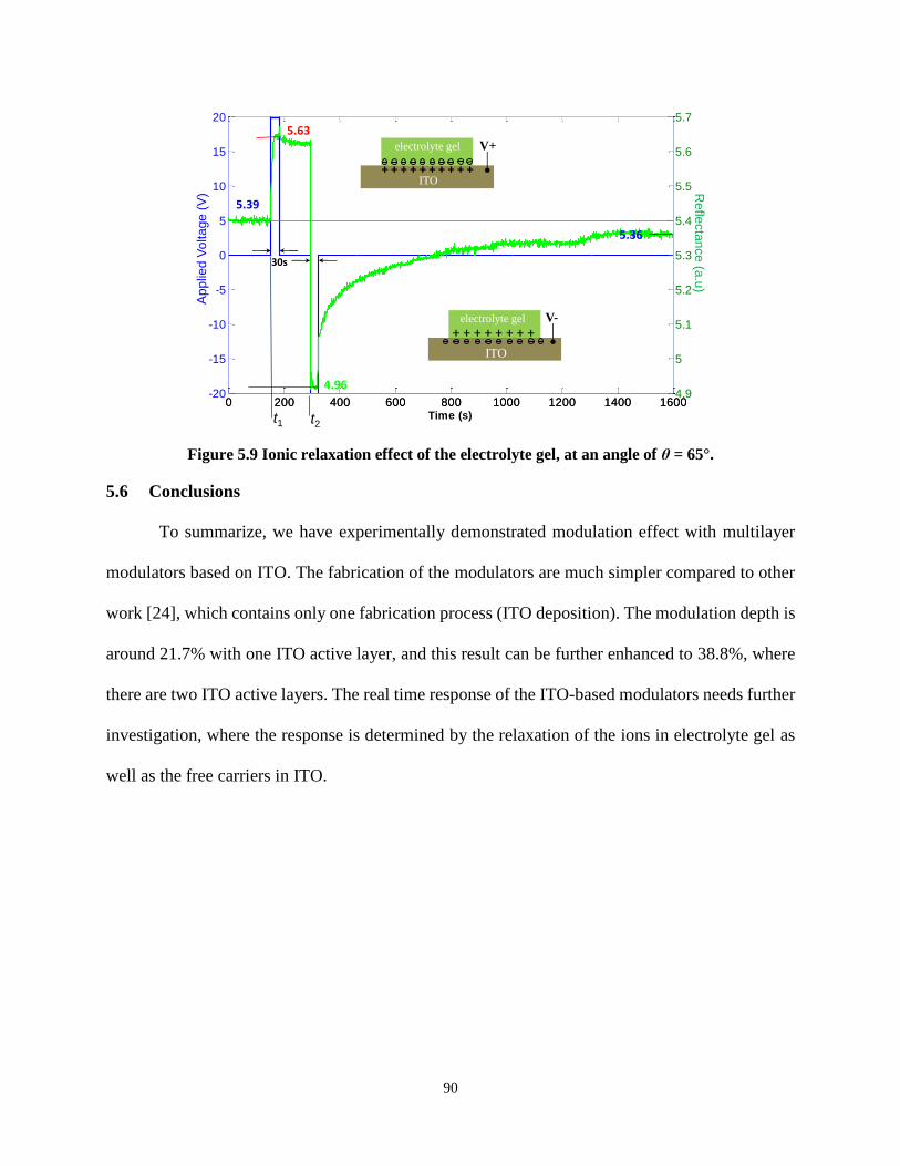
90
Figure 5.9 Ionic relaxation effect of the electrolyte gel, at an angle of θ = 65°.
5.6 Conclusions
To summarize, we have experimentally demonstrated modulation effect with multilayer
modulators based on ITO. The fabrication of the modulators are much simpler compared to other
work [24], which contains only one fabrication process (ITO deposition). The modulation depth is
around 21.7% with one ITO active layer, and this result can be further enhanced to 38.8%, where
there are two ITO active layers. The real time response of the ITO-based modulators needs further
investigation, where the response is determined by the relaxation of the ions in electrolyte gel as
well as the free carriers in ITO.
0 200 400 600 800 1000 1200 1400 1600-20
-15
-10
-5
0
5
10
15
20
Time (s)0 200 400 600 800 1000 1200 1400 1600
4.9
5
5.1
5.2
5.3
5.4
5.5
5.6
5.7
5.39
5.63
4.96
Applie
d V
oltage (
V) R
efle
cta
nce (a
.u)
30s
5.36
t1 t2
electrolyte gel
ITO
V+
+ + + + + + + + + +
electrolyte gel
ITO
V-
+ + + + + + + +

91
6 ULTRACOMPACT ELECTRO-OPTIC
MODULATORS BASED ON ENZ-SLOT
WAVEGUIDE
In this chapter, we will continue the work in Chapter 5 and propose a novel waveguide,
namely “TCO-slot waveguide”, which combines both the tunable property of a TCO and field
enhancement of a slot waveguide. Recent experiments showed that unity-order index change [24]
in a TCO can be achieved in a metal-oxide-semiconductor (MOS) structure by accumulation
charge. However, the ultrathin (~5nm) accumulation layer and inherent absorption of TCOs
impede the practical applications of this effect. We found that light absorption can be sharply
enhanced when the slot dielectric constant is tuned close to zero. Based on TCO-slot waveguides,
efficient electro-absorption modulation can be achieved within 200nm with small insertion loss.
6.1 Introduction
Ultracompact high-speed electro-optic (EO) modulators have become one of the critical
technical bottlenecks impeding the wide applications of on-chip optical interconnects. This is due
to the very poor EO properties of conventional materials. Phase modulators are on the order of
millimeters [209-211] and can reduce to about tens of micrometers by introducing novel structures
to enhance the EO effect [212]. Absorption modulators can be quite compact, but in most cases
they require advanced materials [82,213]. Even though, their dimensions are still 10μm~100μm.
On-chip optical interconnects require EO modulation at the nanoscale. The key to achieve
nanoscale EO modulation is to (1) identify an efficient and low cost active material and (2) greatly
enhance light-active medium interaction based on a novel waveguide or platform.

92
The development of metamaterials has opened new horizons in photonics [11,214]. Recent
research shows that the dielectric constant of materials can be engineered to be almost arbitrary
value (positive, zero, or negative). One example is epsilon-near-zero (ENZ) materials [215-217],
which received significant attention and found applications in squeezing electromagnetic energy
through very narrow channels [218,219], design of matched zero-index materials [217,220], as
well as shaping the radiation pattern of a source [214,221]. In our recent research [222], we found
that light absorption can be greatly enhanced in ENZ-slot waveguides hence ENZ material is very
promising to improve the performance of EO modulators. An ENZ material is found to have many
advantages as an EO material: (1) sharply enhanced absorption can be achieved in an ultrathin slot;
(2) the ultrathin slot does not introduce a large insertion loss; (3) an ENZ material often has tunable
optical properties because a small change in carrier density may result in a significant change in
dielectric constant.
As introduced in Chapter 5, the effect of free carriers on an optical material can be
approximated by the Drude model [201,202], . Here, ε∞ is the high frequency
dielectric constant, γ is the electron damping factor, ω is the angular frequency of the light, and ωp
is the plasma frequency given by , which depends on carrier concentration N, and the
effective electron mass m*. The ENZ effect can be found in many materials at for
example, tungsten at λ0=48.4nm with a minimum |ε(W)|=0.483, and aluminum at λ0=83nm with a
minimum |ε(Al)|=0.035 [39]. However, the plasma frequencies of most metals are located in the
UV regime due to their ultrahigh electron density. To make ENZ located in the near infrared (NIR)
regime, the electron density should reduce to 1020~1021/cm3, which coincides that of TCOs.
Recently, considerable effort has been focused on TCOs as the plasmonic and ENZ metamaterial
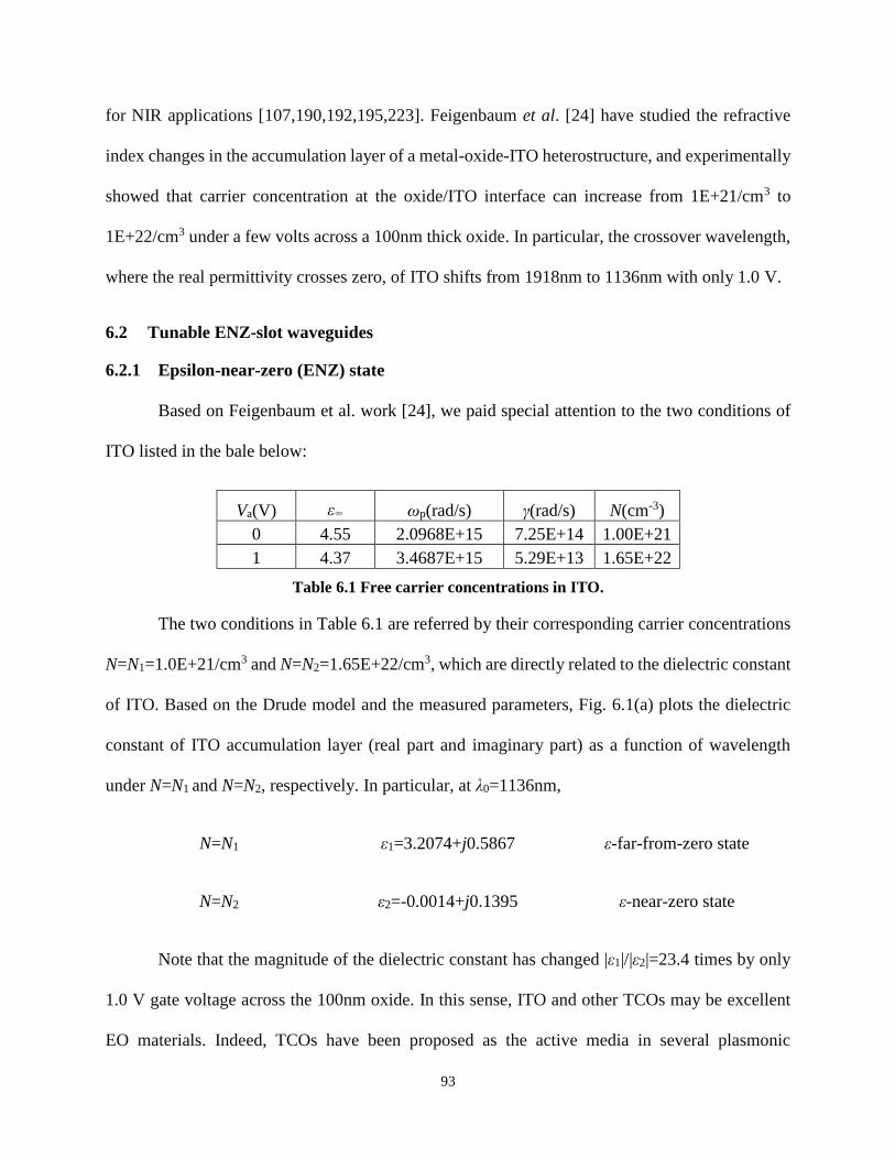
93
for NIR applications [107,190,192,195,223]. Feigenbaum et al. [24] have studied the refractive
index changes in the accumulation layer of a metal-oxide-ITO heterostructure, and experimentally
showed that carrier concentration at the oxide/ITO interface can increase from 1E+21/cm3 to
1E+22/cm3 under a few volts across a 100nm thick oxide. In particular, the crossover wavelength,
where the real permittivity crosses zero, of ITO shifts from 1918nm to 1136nm with only 1.0 V.
6.2 Tunable ENZ-slot waveguides
6.2.1 Epsilon-near-zero (ENZ) state
Based on Feigenbaum et al. work [24], we paid special attention to the two conditions of
ITO listed in the bale below:
Va(V) ε∞ ωp(rad/s) γ(rad/s) N(cm-3)
0 4.55 2.0968E+15 7.25E+14 1.00E+21
1 4.37 3.4687E+15 5.29E+13 1.65E+22
Table 6.1 Free carrier concentrations in ITO.
The two conditions in Table 6.1 are referred by their corresponding carrier concentrations
N=N1=1.0E+21/cm3 and N=N2=1.65E+22/cm3, which are directly related to the dielectric constant
of ITO. Based on the Drude model and the measured parameters, Fig. 6.1(a) plots the dielectric
constant of ITO accumulation layer (real part and imaginary part) as a function of wavelength
under N=N1 and N=N2, respectively. In particular, at λ0=1136nm,
N=N1 ε1=3.2074+j0.5867 ε-far-from-zero state
N=N2 ε2=-0.0014+j0.1395 ε-near-zero state
Note that the magnitude of the dielectric constant has changed |ε1|/|ε2|=23.4 times by only
1.0 V gate voltage across the 100nm oxide. In this sense, ITO and other TCOs may be excellent
EO materials. Indeed, TCOs have been proposed as the active media in several plasmonic

94
modulators [224,225]. However, there seems always a tradeoff between the dimensions and
insertion loss of the modulators. In this work, we show that modulators with ultracompact
dimensions and small insertion loss can be achieved even on a plasmonic platform based on our
recent work on ENZ-slot dielectric waveguides [222].
(a) (b)
Figure 6.1 (a) Real part and imaginary part of the dielectric constant of ITO as a function of
wavelength at two different carrier concentration based on Drude model. (b) The illustration
of ENZ-slot waveguides.
A low carrier concentration (or a voltage between 0 and 1.0 V in Ref. [24]) should result
in ENZ accumulation layer at the telecom wavelengths. However, due to the lack of the
experimental data, we only consider devices working at 1136nm. To circumvent the band edge
absorption of Si at 1136nm in the theoretical and numerical study, the waveguide semiconductor
is assumed to be a material with a similar refractive index of Si at telecom wavelengths, e.g. GaAs.
The applications of the devices described below can be easily extended into telecom Si photonics.
6.2.2 Significantly enhanced absorption by ENZ state
Figure 6.1(b) illustrates the structure to be discussed in this chapter. We will use ITO as
one example of various TCOs. Assume 10nm thick ITO film is sandwiched between two Au slabs
with 30nm thick SiO2 buffer layer. The structure is simply the MOS structure as reported in Ref.
95
[24] with a thinner oxide layer. Optically, it is also known as a metal-insulator-metal (MIM)
plasmonic waveguide, where a well confined transverse magnetic (TM) plasmonic mode can be
excited between the two Au slabs. The magnetic field is parallel to the slabs, i.e. H=Hx in Fig.
6.1(b). At the SiO2-ITO interface, the continuity of normal electric flux density,
(6.1)
is applicable, where the free charge effect is included in the complex dielectric constant. Thus,
very high electric field can be excited when |εITO| 0. In other words, an ENZ-slot can sharply
enhance the electric field in the slot. Without loss of generality, we assume the dielectric constant
of the ENZ-slot to be:
. (6.2)
The dissipation power density:
(6.3)
can be greatly enhanced at ENZ because: (1) |Ey| reaches its maximum and (2) ε"/|ε| nearly grows
to its maximum at the same time. To maximize the absorption, the magnitude of dielectric constant
of the slot should decrease to zero as close as possible. Equation (6.3) is valid for infinitesimal slot
thickness. Otherwise, the guided power will redistribute, and the operation of the slot waveguide
fails if the slot thickness is too large. The absorption of the ENZ-slot may even be much stronger
than that of Au in the waveguide as can be seen in the following context.
Based on the transfer matrix method, we solved the TM mode supported by the Au-ITO-
SiO2-Au stack, i.e. a 2D ITO-slot MIM plasmonic waveguide. The dielectric constant of Au is ε=

96
-63.85+j5.07 at λ0 = 1136nm. We considered two cases: (1) without a gate voltage, N = N1 and the
10nm ITO layer has dielectric constant ε1 = 3.2074+j0.5867; (2) with a suitable gate voltage, N =
N2 and the 10nm ITO layer is split into two, namely 5nm unaffected layer with ε1 = 3.2074+j0.5867
and 5nm accumulation layer with ε2 = -0.0014+j0.1395. As shown in Fig. 6.2(b), the electric field
can be greatly enhanced in the accumulation layer at λ0=1136nm when carrier concentration
increases from N1 to N2. In particular, the magnitude of Ey increases about 9.2 times. In addition,
similar level of enhancement can be achieved when the ENZ-slot is sandwiched in a dielectric
waveguide. Figure 6.2(b) shows the mode profiles of an ENZ-slot dielectric waveguide at N1 and
N2. The top and bottom dielectric layers, each 125nm thick, are assumed to be heavily doped
semiconductor with refractive index 3.45.
(a) (b)
Figure 6.2 (a) The plots of the transverse electric field magnitude across the ENZ-slot MIM
plasmonic waveguide at N=N1 and N=N2, respectively. (b) The plots of the transverse electric
field magnitude across the ENZ-slot dielectric waveguide at N=N1 and N=N2, respectively.
6.3 Nanoscale EO modulators
6.3.1 Mode profiles
These 2D film stacks can be easily rendered into 3D rib waveguide as shown in Fig. 6.3.
We used a 3D mode solver to study their modes based on the finite-difference time domain (FDTD)

97
method. Figure 6.3(a) shows the mode profiles of the ITO-slot plasmonic waveguide at different
carrier concentrations. Note the top Au strip is only 200nm wide. As can be seen, there is a
considerable shift in the effective index: 1.99 at N=N1, and 1.09 at N=N2. Thus, quite compact
phase modulators may be realized. More importantly, there is a huge change in the waveguide
attenuation. At N=N1, the |Ey| in the ITO is even lower than in the SiO2 buffer layers, and the
waveguide works at the low loss state with α1 = 2.92 dB/μm; at N=N2, the |Ey| in the accumulation
layer is many times higher than in the SiO2 buffer layers, and the waveguide works at the high
absorption state with α2=23.56 dB/μm. As a result, modulation depth 20.64 dB/μm can be achieved,
and 3 dB modulation depth only requires 146nm propagation distance. Based on the film stack
shown in Fig. 6.2(b), a dielectric modulator can be designed. Figure 6.3(b) shows the mode profiles
of the ITO-slot dielectric modulator at different carrier concentrations. A similar modulation effect
can be achieved. The dielectric modulator may find more practical applications.
Figure 6.3 The electric field profiles, effective indices, and propagation loss for different ITO-
slot waveguides at N=N1 and N=N2, respectively: (a) in a plasmonic waveguide; (b) in
dielectric rib waveguide. The refractive indices of the semiconductor and SiO2 are assumed to
be 3.45 and 1.45, respectively. All mode profiles are shown in normalized electric fields.
6.3.2 Performance Analysis
To evaluate the insertion loss of the EO modulators, we performed 3D FDTD simulations

98
with the smallest mesh size down to 0.5nm. We first simulated the modulator based on the
plasmonic waveguide platform as shown in Fig. 6.4(a). We assume the modulator is embedded in
a waveguide with same configuration as itself except without the ITO layer. The length of the EO
modulator is 150nm. Figures 6.4(b) and (c) show the power distribution in the waveguide at N=N1
and N=N2, respectively. Simulation results demonstrate that the overall throughput is 89.6% at
N=N1, and 40.8% at N=N2. Note that the insertion loss is only 0.48 dB (89.6%). The achievable
modulation depth, 3.42 dB, is very close to the one predicted by the 3D mode solver. We also
simulated the modulator based on the dielectric waveguide platform as shown in Fig. 6.4(d). The
length of the EO modulator is 200nm. In this case, we assume the modulator is embedded in a
dielectric waveguide with same overall dimensions as itself except without the ITO and buffer
layers. Figures 6.4(e) and (f) show the power distribution in the waveguide at N=N1 and N=N2,
respectively. Simulation results demonstrate that the overall throughput is 88.2% at N=N1, and
39.1% at N=N2. The achievable modulation depth, 3.53 dB, is smaller than the one predicted by
the 3D mode solver. This is due to the mode mismatch between the slot waveguide of the
modulator and its input/output rib waveguide. We expect that its performance (modulation depth
and insertion loss) can be significantly improved by replacing the input/output rib waveguide with
a dielectric slot waveguide.
The design of the EO modulator is ultracompact and has much lower insertion loss
compared with previous works, in which a modulation depth around 3 dB need the modulator
lengths of 4μm [226] and 50μm [82], respectively. In most works, the insertion loss is either not
reported or quite large. For example, the insertion loss is over 3.7 dB in Ref. [82].
In addition, the optical bandwidth of the modulators can be over several THz due to the
slow Drude dispersion [227]. The EO modulators can potentially work at an ultra-high speed,

99
being mainly limited by the RC delay imposed by electric circuits.
Figure 6.4 (a) The illustration of an EO modulator embedded in a plasmonic rib waveguide.
(b,c) The 3D simulation of light propagation between a plasmonic rib waveguide and the EO
modulator at N=N1 and N=N2, respectively. (d) The illustration of an EO modulator
embedded in a dielectric rib waveguide. (e, f) The 3D simulation of light propagation between
a dielectric rig waveguide and the EO modulator at N=N1 and N=N2, respectively. (b), (c), (e)
and (f) are shown in normalized power distribution.
6.4 Conclusions
Recent research shows that transparent conductive oxides (TCOs) are promising tunable
ENZ metamaterials. When sandwiched in a plasmonic or dielectric waveguide, a very thin ENZ
film can greatly enhance light absorption. The tunable ENZ-slot waveguides may enable EO
modulation at nanoscale and an optical modulator can be made at the scale of a transistor. In
addition, the nanoscale modulators potentially have the advantages of small insertion los,

100
ultrahigh-speed, and easy fabrication. A similar work can be found in Ref. [227], where aluminum-
doped zinc oxide (AZO) is the active material. The successfully development of this technique
may lead to a significant breakthrough in on-chip optical interconnects.

101
7 GREATLY ENHANCED ABSORPTION OF
MONOLAYER GRAPHENE IN AN ULTRABROAD
BAND
In Chapter 5 and Chapter 6, we explored the electro-optic (EO) property of ITO and its
potential applications in light modulation. From Chapter 7 to Chapter 8, we will focus on another
natural metamaterial – graphene and investigate its properties which can be employed in
modulators. In this chapter, greatly enhanced light absorption by monolayer graphene over a broad
spectral range, from visible to near infrared, is experimentally demonstrated based on the
attenuated total reflection. In the experiment, graphene is sandwiched between two dielectric
media referred as superstrate and substrate. Based on numerical calculation and experimental
results, the closer the refractive indices of the superstrate and the substrate, the higher the
absorption of graphene will be. The light absorption of monolayer graphene up to 42.7% is
experimentally achieved [205]. Compared to other reported works [248,265-269], our work
doesn’t need any complicated, time-consuming fabrication process and the greatly enhanced
absorption is shown to be broadband.
7.1 Introduction
Graphene [229,230] is the first two-dimensional (2D) atomic crystal available to
researchers, which is a basic building block for graphitic materials of all other dimensionalities
[231], as shown in Fig. 7.1. Since it was isolated by mechanical exfoliation in 2004 [229], many
extraordinary properties of graphene have been demonstrated. For example, graphene can support
remarkably high density of electric currents [232], and has high thermal conductivity [233] and
elasticity [234]. At room temperature, the electron mobility of graphene is extremely high, up to

102
2.5×105 cm2 V-1 s-1 [232,235]. This property enables graphene a desirable material in the
advancement of nanoelectronics [236], for example, metal-oxide-semiconductor field effect
transistor (MOSFET) channels [237], graphene nanoribbons [97,238,239], bilayer graphene
transistor [240] and perforated graphene transistors [241-243]. The optical properties of graphene
have intrigued considerable interest as well. Recent research revealed gate-variable optical
conductivity [244] and high-speed operation [245] of graphene. These extraordinary properties
combining with its high electron mobility make graphene a promising candidate satisfying the
need of broadband optical modulators [78,222,246,247] and photodetectors [245,248].
Figure 7.1 Illustration of the graphene (upper), 0D bucky balls (lower left), 1D nanotubes
(lower middle), and 3D graphite (lower right). [231]
7.2 Optical Absorption of Graphene and Its Applications
The optical property of graphene is attracting researchers’ interests. The light transmission
(T) of a free standing monolayer graphene could be derived with Fresnel’s equation for a thin film
with a fixed universal optical constant [232,247] of , to be:
103
(7.1)
where is the fine structure constant [249]. The reflectivity of graphene is
very low (< 0.1%), therefore nearly 2.3% of the incident light will be absorbed by the graphene
thin film, which is independent of the wavelength [244,249-251]. The absorption spectrum of a
single layer graphene is quite flat for a wide wavelength range, from 300 to 2,500nm [252]. The
large transmission combines the high conductivity, makes graphene a promising candidate in a
variety applications, including solar cells, touch screens and organic light-emitting diodes
(OLEDs). Indium tin oxide (ITO) is widely used in the above mentioned devices. Despite that ITO
has an optical transparency of nearly 90% and a low sheet resistance (less than 100 Ω/, which
depends on process condition), it is brittle and expensive. With stable doping to increase
conductivity and a controlled layer number, graphene could replace ITO as the transparent
electrode in solar cells [253,254]. Graphene may also work as photoactive material [255] and the
channel [256] in photovoltaic devices.
Graphene can be used with metals in the form of graphene/metal contacts in photo detectors
[245], since it has a very wide spectrum of absorption and fast carrier transport. A Schottky-like
barrier at a graphene/metal contact will be set up and generate a built-in electric field. Electron-
hole pairs generated near the contact will be separated by the electric field and a net photocurrent
can be observed [257-260]. Recently, interdigitated metal electrodes made of two different metals
are employed in a graphene photo detector [261]. The design allows photo detection over the entire
area of the device. Reliable detection of optical data streams of 1.55μm light pulses at a rate of 10
GBits/s can be obtained in this device [261].

104
7.3 Enhanced Optical Absorption by Graphene
7.3.1 Background
Considered its single atom thickness, the interaction between light and graphene is quite
strong: light absorption can go up to = 2.293% (α is the fine-structure constant) [232,262-264]
when light is normal incident through graphene. However, the absolute value (~2.3%) of
absorption is still weak for most practical applications. For active optoelectronic devices
[245,261,265], a strong light-matter interaction is usually desired. Therefore, many approaches
have been explored to increase the interaction of light with graphene or to enhance the optical
absorption. One possible way is to utilize plasmonic nanostructures [265] or nanoparticles [266]
in graphene-based photodetectors, where the responsivity can be significantly enhanced due to the
localized surface plasmons. It was also shown that the enhanced absorption of graphene can be
achieved by patterning doped-graphene into a periodic nanodisk [267] or alternating with insulator
layers to form superlattice structure [268]. More recent research work demonstrated that over 60%
absorption can be reached by integrating graphene with a microcavity structure [248]. However,
all these methods mentioned above either need complicated, time-consuming fabrication processes
[248,269] or the devices exhibit very narrow bandwidth [248,266,269] due to the involvement of
microcavities or resonators. An easily fabricated graphene-based device with a broad bandwidth
is then desired for fundamental research and practical applications.
In a recent research [270], up to 10% light absorption by a monolayer graphene was
demonstrated through an F2 prism coupling into a graphene-sandwiched silica waveguiding
structure. The experimental setup used in Ref. [270] is based on an attenuated total reflection (ATR)
configuration. This configuration has been used to measure the graphene absorption spectra [270],
analyze terahertz surface plasmons on graphene [272], and estimate number of carbon layers in an
unknown graphene sample [273].

105
7.3.2 Numerical Analysis
Here we consider a graphene-sandwiched three-layer structure as shown in the inset of Fig.
7.4(a). The top layer (superstrate), graphene, and bottom layer (substrate) have refractive indices,
n1, n2, and n3, respectively. Assume that a plane wave is incident into the three-layer structure and
the corresponding propagation angles to the normal are θ1, θ2, and θ3, respectively. Snell’s law is
held between layers, (q=1, 2, 3). Based on the transfer matrix method
(TMM) [197-199], the amplitude reflectance can be calculated by:
(7.2)
where 𝜑 , k0 is the wavenumber of the light wave in free space; d ≈ 0.335 nm is
the thickness of graphene). Also, (q=1, 2, 3) for s-polarized light, and
(q=1, 2, 3) for p-polarized light.
Figure 7.2 (a) Numerical calculation of the reflectance and absorption as functions of incident
angle, θ1, and substrate refractive index n3. (b) Calculation of maximum achievable
absorption as a function of substrate refractive index n3. Results in (a) and (b) are obtained at
λ=650nm for s-polarized light, and n1=1.51. [205]
For pristine graphene, its surface conductivity σg can be universally expressed as
where h is the plank constant and e represents the elementary charge. Thus,
Ab
sorp
tio
n
106
the refractive index of graphene is a complex number and can be calculated by ,
where ε0 is the permittivity of the free space, and ω is the angular frequency of the incident light
wave.
We assume the refractive index of the superstrate is n1 = 1.51 at λ = 650nm, and first
consider the s-polarized light case. The solid lines in Fig. 7.2(a) plot the power reflectance 𝑅 =
|𝑟|2as a function of incident angle θ1 and substrate refractive index. Based on the transfer matrix
method [197-199], we can similarly calculate the power transmittance T. The absorption A=1-R-
T. The dashed lines in Fig. 7.2(a) plot the A-θ1 relations for different substrates. Almost identical
curves can be obtained at λ = 1520nm or even longer wavelengths if n1 and n3 remain the same as
their corresponding values.
From the graph, we can see that the maximum absorption occurs at the critical angle
for each case. This can be explained as follows. Due to the ultrathin thickness of
graphene, the three-layer structure can also be approximately treated as a two-layer (n1|n3) structure,
with the boundary replaced by graphene as a perturbation, if the graphene absorption is not
significant. According to the continuity relation of electric field in different layers, the electric
field in graphene, E2, is proportional to the amplitude transmittance between the superstrate and
substrate:
, (7.3)
where Ei is the electric field of the incident light wave. The power dissipation in graphene in a unit
area can be calculated by , and maximum |E2| gives rise to maximum pd. In Eq. (7.3),
|E2| reaches its maximum, 2|Ei|, when cos 𝜃3 = 0 or equivalently .

107
Furthermore, the closer n3 and n1 are, the larger the critical angle, and the larger the
absorption. The reason is because a larger critical angle decreases the incident power density on
graphene, , which will increase the ratio between dissipated power and
incident power, i.e.
where η1= η0/n1 is the impedance of the superstrate and η0 = 120 π(Ω) (the impedance of the free
space). For normal light incidence into graphene suspended in air, in Eq. (7.4).
When the absorption becomes significantly large, the amplitude transmittance cannot be estimated
based on the above equation. Instead, the three-layer model needs to be applied.
Based on the three-layer model, the absorption grows with the increase of n3, as shown in
Fig. 7.2(b). The closer n3 to n1(-), the larger the absorption is. For example, the absorption can reach
79.6% when n3=1.509. However, when n3>n1, the maximum absorption will sharply drop. In our
work, we only consider the cases where n1>n3. The power transmittance T=0 when 𝜃1 ≥ 𝜃𝑐; thus,
the incident power will be either reflected back or absorbed by graphene, i.e. A=1-R. The scattering
by graphene is negligible as can be seen in the experimental result for p-polarized light. In other
words, when 𝜃1 ≥ 𝜃𝑐, the absorption can be easily measured by testing the reflectance.
Furthermore, there is no cavity or resonant component involved in the structure. As a result,
the absorption expression given in Eq. (7.4) is not an explicit function of frequency, which implies
that the same level of enhanced light absorption can be achieved in a broad band. This is verified
by the more accurate calculation based on the three-layer model: the absorption would slightly
increase from 39.1% at 650nm to 39.2% at 1620nm if there were no material dispersion (n1 and n2
are actually slowly varying functions of frequency due to material dispersion). Consequently,

108
greatly enhanced ultrabroad band light absorption can be achieved simply based on the graphene-
sandwiched three-layer structure.
7.3.3 Experimental Results and Discussion
To experimentally demonstrate the greatly enhanced light absorption by graphene, we have
built an ATR setup in the Kretschmann configuration [197], as illustrated in Fig. 7.3. A collimated
laser beam propagates through a broadband polarizer (P1) to choose either s- or p- polarized light,
and is then split into two by a beam splitter (BS). One beam is used for recording source power
fluctuation and fed into a germanium photodiode (PD2); another is incident at the angle θ1 into a
BK7 glass hemicylindrical (Ø100mm obtained from Rocoptonics) lens, which functions as a
coupling prism in this setup. The reflected light is then collected by another germanium photodiode
(PD1). The power ratio between PD1 and PD2 can well measure the reflectance, R, even if there
is power fluctuation in the laser source. The rotation of the prism (together with the graphene
sample) and PD1 is in a θ1-2θ1 configuration, which is precisely controlled by two motorized
rotation stages. In our experiment, we made one measurement for every 0.25° increment of θ1. As
a result, the reflectance, R, as a function of θ1 can be plotted.
Figure 7.3 Illustration of the experimental setup for ATR measurement. The red dashed line
represents the monolayer graphene film. P1 and BS represent the polarizer and beam
splitter, respectively. [205]
109
Our sample is commercially available monolayer graphene [274] synthesized by the
chemical vapor deposition (CVD) process then transferred to our bare BK7 glass slide. Its Raman
spectroscopy result shown in Fig. 7.4 indicates that the sample is monolayer graphene with an
obviously higher 2D peak than the G peak [275]. The graphene sample is mounted at the back of
the hemicylindrical prism. To avoid a thin air gap between the prism and the graphene sample, a
BK7 index matching liquid is applied between them. In this case, the superstrate can be simplified
and treated as a BK7 medium, consisting of the BK7 prism and the BK7 glass slide. The medium
on the other side of the graphene is referred as the substrate, which is another matching liquid from
CargilleTM in our case to better control the refractive index. A thick (>10 mm) glass plate is used
to hold the matching liquid and meanwhile to deflect light away from PD1.
Figure 7.4 Raman spectroscopy result for the graphene sample. The three curves represent
three different points on the same sample. [274]
In our work, we focused on s-polarization and carried out the experiment in a step-by-step
fashion. First, we tested the graphene on BK7 glass sample without any substrate (or air as the
110
substrate), as shown in Fig. 7.3 but without the deflector. The experimentally measured reflectance
at λ = 650nm and 1520nm as a function of θ1 is shown in Fig. 7.5(a) and (b), respectively. In order
to calculate the absorption of the monolayer graphene, the reflectance (blue triangles) of a bare
BK7 glass slide is measured as a control experiment. The critical angle is measured to be 41.00°
(at λ=650nm) and 41.25° (at λ=1520nm), which is in agreement with the theoretical calculation
value 41.3° (at λ=650nm) and 41.8° (at λ=1520nm). The discrepancy is attributed to the angle error
in θ1, and corrected in our following calculation.
Figure 7.5 Reflectance of a reference BK7 glass slide (blue triangles), monolayer graphene
(red circles), and numerical fit (green) with an s-polarized light (a) with wavelength of λ =
650 nm and (b) λ = 1520 nm. In the legend, “G” represents “graphene”. “BK7/G/air”
means the result with the BK7(prism)-graphene-air configuration. [205]
In each plot, both the reflectance curves are normalized by the average value of the total
internal reflection part in the reference curve. Therefore, the red curve represents the reflectance
of the monolayer graphene. At the critical angle, the absorption of the monolayer graphene can be
calculated as A=1-R, which is 7.6% (at λ=650nm) and 9.8% (at λ=1520nm). The measured
reflectance of the monolayer graphene is numerically fitted (green curve in Fig. 7.5) by calculating
the reflectance through the three-layer structure based on the transfer matrix method (TMM) [197-
199]. In the numerical fitting, the BK-7 medium has a refractive index of n=1.50 at λ=1520nm.

111
We use the dielectric constant of graphene (imaginary part) as the fitting parameter to approach
the measured reflectance data. The result turns out that the dielectric constant of graphene εg=
1+j15.96 or surface conductivity σg=6.22×10⁻⁵S at λ=1520nm. We attribute the discrepancy
between the fitted value and the theoretical value calculated by Eq. (7.2) to the doping in graphene.
A slightly smaller conductivity can also be fitted for the result measured at λ=650nm.
Based on the same sample and configuration, we also measured the absorption of graphene
at longer wavelengths up to 1620nm. At the critical angle, the absorption of monolayer graphene
is in the range of 7.6%-11.2%, which is 3~5 times stronger than the widely known absorption
coefficient (~2.3%). When the incident angle is larger than the critical angle, the reflectance of
graphene is observed to gradually increase and projected to be 100% at θ1 = 90º.
Figure 7.6 (a) Normalized measured reflectance of the monolayer graphene with M1.50 as
substrate under s-polarized light incidence at λ=650nm. (b) Measured reflectance of the
monolayer graphene with M1.50 as substrate under s-polarized light incidence at λ=1520nm.
In both graphs, red curves represent the results when a BK7 deflector is used; blue curves
represent the results when a BSG deflector is used. In the legend, “G” and “M” represent
“graphene” and “matching liquid”, respectively. “BK7/G/M/BK7” means the result for the
BK7(prism)-graphene-M1.50(substrate)-BK7(deflector) configuration. [205]

112
The absorption of the monolayer graphene can be further enhanced when the refractive
index of the substrate increases. In our work, a matching liquid with refractive index 1.50 (at
λ=589.3nm according to the manufacturer; referred as “M1.50”) is applied as the substrate of the
graphene. Two different supporting glass deflectors, BK7 and borosilicate glass (BSG), are
separately used to hold the substrate M1.50. In Fig. 7.6, triangle points are the control experiments
measured by “removing” the graphene. Both the curves measured with graphene sample are
normalized with the corresponding control curves.
In the control experiment with BK7 deflector, the total internal reflection occurs at the
interface of the superstrate BK7 and the substrate M1.50, θC ≈ 81.75°. As shown in the red dot
curve, at θC the absorption of monolayer graphene is measured as 42.7%, which is ~18 times
stronger than the widely known absorption (~2.3%).
This result is further confirmed by replacing the BK7 deflector with the BSG deflector and
repeating the measurement, as shown in the blue dot curves in Fig. 7.6(a), where the absorption is
measure as 40.5%. In this configuration, there are two total internal reflections: first one occurs at
the interface of the substrate M1.50 and BSG deflector with a critical angle θC1 ≈ 76.75°, and the
second one occurs at the interface of the superstrate BK7 and the substrate M1.50 with θC2 ≈ 81.75°.
Beyond θC2, the blue dot curve is in a good agreement with the red dot curve, and both indicate the
reflectance of the monolayer graphene in the sandwich configuration. The oscillation of the blue
triangle curve between the two angles θC1 and θC2 is due to the substrate M1.50 functioning as a
cavity between the graphene and BSG deflector.
Similarly, R-θ1 relation at different wavelengths is measured. Figure 7.6(b) shows the
results for the measurement at λ=1520nm. The absorption is about 35.3% at the critical angle.
When the wavelength varies from 650nm to 1620nm, the absorption gradually decreases from 40.5%

113
to 33.1% with the BSG deflector, and from 42.7% to 35.3% with the BK7 deflector. Thus,
ultrabroad band enhanced light absorption is achieved. The variation of the absorption with the
wavelength can be attributed to the dispersion of the superstrate BK7 and substrate M1.50. In
particular, the absorption becomes more sensitive when n1 and n3 are close enough. When the
substrate is replaced by M1.49 matching liquid, the absorption will considerably decrease, for
example, dropping from 42.7% to 28% at λ=650nm.
Figure 7.7 For 1520nm p-polarized light incidence, the normalized measured reflectance by
the monolayer graphene sample as a function of incident angle when (a) the substrate is air,
and (b) the substrate is M1.50. [205]
The enhanced absorption of graphene is shown to be very sensitive to the polarization of
the incident light. Similar as previous experiments, we measured the reflectance of the monolayer
graphene when the substrate is air and M1.50 separately with p-polarized incident light. As can be
seen in Fig. 7.6, the maximum absorption does not occur at the critical angle and is not sensitive
to the substrate refractive index. The minimum reflectance beyond the corresponding critical angle
is 97.65% (when the substrate is air) or 97.7% (when the substrate is M1.50), respectively.
Therefore, the absorption in both cases is calculated as ~2.3%, which is similar as the widely
70 75 80 85 900
0.2
0.4
0.6
0.8
1.0
1(degree)
Re
fle
cta
nce
BK7/M/BK7
BK7/G/M/BK7
20 30 40 50 60 70 800
0.2
0.4
0.6
0.8
1.0
1(degree)
Re
fle
cta
nce
BK7/air
BK7/G/air
(a) (b)
114
known absorption coefficient. The reason is because the electric field in graphene for p-polarized
incident light cannot be estimated by Eq. (7.3), instead
. (7.5)
where E2t and E2n represents the tangential and normal components of the electric field in graphene.
Therefore, when , and , which is opposite to that case for
s-polarized light. In the latter case, E2 = E2t gains its maximum when .
7.4 Conclusions
In this work, we have experimentally demonstrated that the absorption of monolayer
graphene can be significantly enhanced over a broad spectral range, from visible to infrared, when
the incident light is s-polarized. At the critical angle, the absorption is in the range of 7.6%-11.2%,
when the substrate is air, and up to 42.7%, when the substrate is replaced by a medium with a
closer refractive index compared to that of the superstrate. The enhanced absorption is not strongly
dependent on the wavelength but very sensitive to the polarization of incoming light. The
significantly enhanced absorption of monolayer graphene may have potential applications in
broadband photodetectors and solar cells.
115
8 NANOSCALE ELECTRO-OPTIC MODULATORS
BASED ON GRAPHENE
Research on graphene has revealed its remarkable electro-optic properties, which promise
to satisfy the needs of future electro-optic modulators. However, its ultrasmall thickness, compared
with operating light wavelength, downplays its role in an optoelectronic device. The key to achieve
efficient electro-optic modulation based on graphene is to enhance its interaction with light. To
this end, some novel waveguides and platforms will be employed to enhance the interaction. In
this chapter, we will continue the work in Chapter 7 and present the recent exploration of graphene
electro-optic modulators based on graphene sandwiched in dielectric or plasmonic waveguides
[222]. With a suitable gate voltage, the dielectric constant of graphene can be tuned to be very
small due to the effect of intraband electronic transition, resulting in “graphene-slot waveguides”
and greatly enhanced absorption modes. Up to 3 dB modulation depth can be achieved within
800nm long silicon waveguides, or 120nm long plasmonic waveguides based on three-dimensional
numerical simulations. They have the advantages of nanoscale footprints, small insertion loss, low
power consumption, and potentially ultrahigh speed, as well as being CMOS-compatible.
8.1 Introduction
Surface plasmon polaritons (SPPs) are collective oscillations of electrons at the interface
of dielectric/metal, which can be excited by photon or electron. Usually, noble metals (Au or Ag)
are used as the plasmonic materials. However, high loss and non-tunability are the main
disadvantages of the devices fabricated with these materials. As a rising star, graphene has been
proposed as a new platform for plasmon waveguiding at infrared frequencies [68-74], and also
considered as terahertz metamaterials [75]. SPPs excited in graphene have many promising

116
properties [72,276], for example, extremely strong confinement, tunability with electrical gating
or chemical doping, and low loss. Hence, graphene is an attractive alternative to traditional
plasmonic materials. Graphene as plasmonic material has been demonstrated in light harvesting
[277], optical biosensing [278], and transformation optics [76]. The tunability of graphene-based
plasmonic devices originates from its complex dynamic conductivity determined by the Kubo
formula [73,76,77], which will be discussed in the following section of this chapter. Simply
speaking, the imaginary part of the conductivity σ" may has a negative or positive value which
depends on the chemical potential of graphene at different frequency ranges, and it plays an
important role in supporting different types of surface waves. With a low chemical potential,
graphene has a negative σ", leading to a semiconductor-like behavior, capable of guiding a proper
TE surface wave. With a large chemical potential (|μ|>ħω/2), σ" is positive and graphene will
behave like metal and support a proper TM surface wave, which shows similar behavior as noble
metals [279-282].
8.2 Intraband absorption of graphene
8.2.1 Surface conductivity model of graphene
Graphene can be modeled as an infinitesimally-thin, local two-sided surface characterized
by a surface conductivity σ (ω, μc, Γ, T), where ω is radian frequency, μc is chemical potential, Γ
is scattering rate, and T is temperature. The conductivity of graphene can be expressed by the Kubo
formula [73,76,77],
(8.1)
where e is the charge of an electron, ħ=h/2π is the reduced Planck’s constant,
is the Fermi-Dirac distribution, and kB is Boltzmann’s constant. The local

117
conductivity is isotropic, where there is no external magnetic field is present. The first term in Eq.
(8.1) is contributed by intraband absorption, and the second one by interband absorption.
From equation (8.1), the surface conductivity of graphene can be simplified as σ = σintra(ω,
μc, Γ, T) + σinter(ω, μc, Γ, T). The chemical potential μc is determined by the carrier density ns
, (8.2)
where vF ≈ 9.5E+5 m/s is the Fermi velocity. By applying a gate voltage or chemical doping, the
carrier density can be easily controlled. Thus, the conductivity of graphene can be dynamically
tuned by gate voltage VD in real time. Basically, when μc < ℏω∕2, interband absorption dominates
and graphene becomes absorptive; otherwise, quite transparent. Electrically switching on/off
graphene interband absorption plays a key role in the modulator reported in Ref. [247].
The intraband term in Eq. (8.1) can be written as
(8.3)
and the interband term can be approximated for ,
(8.4)
The complex surface conductivity can be simply expressed as , as mentioned
in the introduction part, at low frequency regimes, a proper TE surface wave exists only if 𝜎" > 0
(associated with intraband absorption), and a proper TM surface wave exists for 𝜎" < 0 (associated
with interband absorption) [283].
8.2.2 Intraband absorption
We found the intraband absorption can be equally important in a graphene absorption

118
modulator. Based on Eq. (8.1), we calculated the graphene conductivity at T = 300K (scattering
rate, ℏΓ = 5 meV) [247]. Figures 8.1(a) and 1(b) plot the real and imaginary parts of the
conductivity as a function of the chemical potential and wavelength in the near-infrared regime.
In particular, the real part of conductivity is very sensitive to chemical potential; for example, at
wavelength λ0 = 1550nm, varying from nearly 60.85μS to 1.37μS when chemical potential rises
from 0 to 0.6eV, as shown in Fig. 8.1(c). Figure 8.1(c) also shows how interband absorption and
intraband absorption contribute to the graphene conductivity, respectively. Figure 8.1(d) plots the
corresponding dielectric constant (real part, imaginary part, and magnitude),
, where Δ = 0.7nm is the effective thickness of graphene [247]. The dielectric
constant of graphene varies from εeff (0 eV) = 0.985 + j8.077 to εeff(0.6 eV) = −2.508 + j0.182 at
λ0 = 1.55μm. Note the sign of real part flips due to intraband absorption because the interband
absorption and intraband absorption contribute to the imaginary part of conductivity with different
signs, as shown in Fig. 8.1(c). As a result, there is a dip in the curve of dielectric constant
magnitude, where “metallic graphene” is transforming to “dielectric graphene” with Refεeff = 0.
In this case, the “transition chemical potential” is μt = 0.515 eV and |εeff(μt)| = |− 0.048 + j0.323| =
0.327, which means the magnitude varies |εeff(0)|/|εeff(μt)| ≈ 25 times. Note this “epsilon-near-zero”
[218,219,284] effect can be seen almost in any material at its plasma frequency; for example, Ag
at λ0 = 326nm. The uniqueness of graphene lies in that its plasma frequency can be tuned by
electrical gating.

119
Figure 8.1 (a) Real part and (b) imaginary part of the graphene conductivity as a function of
chemical potential and wavelength (T = 300K) based on the Kubo formula. (c) The graphene
conductivity (real part and imaginary part), by interband transition and intraband
transition, as the function of chemical potential at λ0 = 1550nm. (d) The effective dielectric
constant (real part, imaginary part, and magnitude) as a function of chemical potential at λ0 =
1550nm. (e) The illustration of a 2D “graphene-slot waveguide” with a 10nm thick Si3N4
buffer layer on each side of graphene. (f) The plots of the transverse electric field magnitude
across the waveguide at μc = 0 and μc = μt, respectively. [222]
8.3 Design and modeling
8.3.1 Significantly enhanced absorption in graphene-slot waveguide
The effect of dielectric constant change is not very manifest when graphene is placed on
top of a dielectric waveguide. Based on the change of dielectric constant, we solved the transverse
magnetic (TM) modes of graphene on a 250nm by 600nm silicon waveguide with a 7nm Al2O3
buffer layer at λ0 = 1.53μm when chemical potential is 0 and μt, respectively. The effective indices

120
are both 2.06, but the attenuation rates are significantly different, 0.134 dB∕μm for μc = 0 and 0.044
dB∕μm for μc = μt. The mode profiles are shown in Fig. 8.2(a) and (b), respectively. The absorption
can be further reduced when μc shifts from 0.515 eV to 0.6 eV or higher. The resulting modulation,
0.09 ∼ 0.13 dB∕μm, coincides with the recent experimental work [247].
Figure 8.2 Mode profiles for graphene on top of dielectric waveguide. [247] (a) At μc = 0,
attenuation α= 0.134dB/μm, and (b) at μc = 0.515 eV, attenuation α= 0.044dB/μm. Both
figures are shown in normalized electric fields.
The absorption of a TM mode can be greatly enhanced when graphene is sandwiched inside
the silicon waveguide, forming a “graphene-slot waveguide,” as illustrated in Fig. 8.1(e). In a slot
waveguide [285], the magnitude of transverse electric field |Ey| is roughly inversely proportional
to that of the dielectric constant. The power absorbed in a unit area, ∙
, can be greatly enhanced at μc = μt because (1) |Ey| reaches its maximum, and (2)
Imεeff/|εeff| nearly grows to its maximum at the same time, as shown in Fig. 8.1(d). To verify this,
we first consider the multilayer stack, as illustrated in Fig. 8.1(e), where graphene is sandwiched
in a silicon waveguide with a 10nm Si3N4 buffer layer on each side. Based on the transfer matrix
method, we find the optimal silicon thickness to enhance light absorption is about 150nm. Figure
8.1(f) plots the |Ey| profiles at μc = 0 and μc = μt, respectively. The absorption is roughly
proportional to |Ey|, with an enhancement about 25 times. In our case, μc = 0 is the transparence

121
state, while μc = μt is the absorption state, which are exactly opposite to the operation principle of
the EO modulator reported in Ref. [247] as well as the graphene-sandwiched devices proposed in
a recent review article [286]. In those devices, the electric field strength for the two states is at the
same level and the imaginary part of graphene dielectric constant determines the absorption.
Graphene has higher conductivity (and larger imaginary part of dielectric constant) at μc = 0.
8.3.2 Mode profiles
Once the configuration of the graphene-slot waveguide is optimized, we use a three-
dimensional (3D) mode solver to determine the optimal waveguide width based on the finite-
difference time-domain (FDTD) method. Considering the fabrication tolerance, the optimal width
of the waveguide is found to be 450nm. Figure 8.3(a) shows the mode profiles of the graphene-
slot waveguide at different chemical potentials. There is only a slight shift in the effective index:
2.032 at μc = 0, and 2.034 at μc = μt. In contrast, there is a huge change in the waveguide attenuation.
At μc = 0, the |Ey| in the graphene is even lower than in the Si3N4 buffer layers, and the waveguide
works at the low loss state with α0 = 0.183 dB/μm; at μc = μt, the |Ey| in the graphene is many times
higher than in the Si3N4 buffer layers, and the waveguide works at the high absorption state with
αv = 4.603 dB/μm. As a result, modulation depth 4.42 dB/μm can be achieved, and 3 dB modulation
depth only requires 679nm propagation distance. An 800nm propagation distance results in
modulation depth 3.54 dB. Therefore, a graphene EO modulator can be made on the nanoscale.
For the sake of easy fabrication, the silicon modulator can also take the form of an asymmetric slot
waveguide, as shown in Fig. 8.3(b). There is only a slight change in the performance.

122
Figure 8.3 The transverse electric field profiles, effective indices, and propagation loss for
different graphene-slot waveguides at μc = 0 and μc = μt, respectively: (a) in a dielectric
waveguide (Si waveguide is 450nm wide and 150nm thick for each layer); (b) in a dielectric
strip waveguide (strip Si waveguide is 450nm wide and 150 nm thick for each layer); (c) in a
metal-insulator-metal waveguide (waveguide is 200 nm wide); (d) in a metal strip waveguide
(strip metal is 200nm wide); (e), (f) in photonic-plasmonic hybrid waveguides [waveguide is
400 nm wide in (e) and 200 nm wide in (f), Si layer is 130 nm thick for both structures]. All
mode profiles are shown in normalized electric fields. The refractive indices of Si, Si3N4, and
SiO2 are assumed to be 3.47, 1.98, and 1.44, respectively. [222]
Furthermore, recent work shows that highly confined modes can be achieved in plasmonic
waveguides [287]. Based on nanoplasmonic platforms, the dimensions of a graphene modulator

123
should be even smaller. Following the same approach, we investigated the interaction between
graphene and various plasmonic modes. Figures 8.3(c) and 8.3(d) list the guided mode profiles,
effective indices, and attenuation of graphene-slot waveguides based the metal-insulator-metal
plasmonic platform. Because of the close interaction between metal and graphene, the chemical
potential with highest absorption shifts to 0.518 eV. Figures 8.3(e) and 8.3(f) list the mode
calculation of graphene-slot waveguides based on the hybrid plasmonic platform. Although Au or
Ag may decrease the metal absorption of the plasmonic waveguides, CMOS-compatible metal, Cu,
is used in all plasmonic modulators, and its dielectric constant is assumed to be −67.86 + j10.01.
A 10nm thick Si3N4 buffer layer is designed on each side of graphene for all plasmonic waveguides
shown in Figs. 8.3(c)–8.3(f). As can be seen in Fig. 8.3(d), a 3 dB (3.82 dB at 1550nm) EO
modulator can be made within 120nm using the metal strip plasmonic waveguide, where the
attenuations are 6.76 dB/μm at μc = 0, and 38.59 dB/μm at μc = 0.518 eV.
8.4 Performance analysis
8.4.1 Insertion loss
To evaluate the insertion loss of the EO modulators, we performed 3D FDTD simulations
with the smallest mesh size down to 0.35nm. In the simulations, we assume the modulators are
embedded in the same waveguide as themselves except without the sandwiched graphene. We first
simulated the modulator based on the silicon waveguide platform, as shown in Fig. 8.4(a). The
length of the graphene modulator is 800nm. Assume the thickness of the bottom silicon layer for
electrical contact is negligible. Figures 8.4(b) and 8.4(c) show the power distribution in the
waveguide at μc = 0 and μc = 0.515 eV, respectively. Simulation results demonstrate that the overall
throughput is 92.0% at μc = 0, and 42.5% at μc = 0.515 eV. Note that the insertion loss is only 0.36
dB (92.0%). The achievable modulation depth, 3.4 dB, is slightly smaller than the one predicted

124
by the 3D mode solver. We also simulated EO modulators based on the guided modes listed in
Figs. 8.3(b)–8.3(f). The results are similar as predicted in the mode solver. As one example, Figs.
8.4(e) and 8.4(f) show the simulation results at μc = 0 and μc = 0.518 eV for the plasmonic
modulator illustrated in Fig. 8.4(d). The overall throughput is 81.04% at μc = 0, and 36.92% at μc
= 0.518 eV. Note that the overall length is only 120nm, while the modulation depth is 3.4 dB.
Figure 8.4 The illustration of a graphene EO modulator based on a silicon waveguide. (b), (c)
The 3D simulation of light propagation between a silicon waveguide and the EO modulator at
μc = 0 and μc = μt, respectively. (d) The illustration of a graphene EO modulator based on a
metal strip plasmonic waveguide. (e), (f) The 3D simulation of light propagation between a
metal strip plasmonic waveguide and the EO modulator at μc = 0 and μc = μt, respectively.
Figures (b), (c), (e) and (f) are shown in normalized power distribution. [222]
8.4.2 Bandwidth
On-chip optical interconnects require a broad bandwidth. Although the conductivity of
graphene only weakly depends on the working frequency, the effective dielectric constant,
, is a function of working frequency. As a result, in terms of dielectric constant,
graphene is a dispersive medium. Nevertheless, we found the effect of dispersion is not so obvious.

125
We studied the bandwidth of the EO modulators by solving the modes shown in Fig. 8.3 at different
working wavelengths. Figure 8.5(a) shows the waveguide absorption as a function of wavelength
in a silicon waveguide. As can be seen, the attenuation of the modulator at μc = 0 nearly remains a
constant, 0.18 − 0.20 dB/μm, while the attenuation at μc = 0.515 eV decreases when the wavelength
shifts away from 1550nm. In particular, the attenuations are 4.44dB/μm, 4.60dB/μm, and
4.45dB/μm at 1545nm, 1550nm, and 1555nm, respectively. Wavelength spanning from 1545nm
to 1555nm, or 1.25THz bandwidth, only decreases modulation depth 0.16 dB/μm. For our 800nm
silicon modulator, the decrease will be 0.14 dB. The prediction was further verified by 3D FDTD
modeling. At μc = 0, the overall throughput is 92% for both 1545nm and 1555nm; at μc = 0.515
eV, the overall throughput is 43.7% and 43.6%, for 1545nm and 1555nm, respectively. Thus, this
modulator has a 3 dB bandwidth at least 1.25 THz.
We also studied the bandwidth of our EO modulators based on plasmonic waveguides.
Figure 8.5(b) shows the waveguide absorption as a function of wavelength in a metal strip
plasmonic waveguide based on the 3D mode solver. As can be seen, when wavelength shifts ±
5nm away from 1550nm, the attenuation decreases about 1.9 dB/μm. Within 120nm, the
modulation depth changes 0.23 dB, from 3.82 dB to 3.59 dB. Thus, this EO modulator also allows
for over a terahertz bandwidth. The calculation was also further verified by 3D FDTD modeling.
At μc = 0, the overall throughput is 81% for both 1545nm and 1555nm; at μc = 0.518 eV, the overall
throughput is 37.84% and 37.58%, for 1545nm and 1555nm, respectively.

126
Figure 8.5 The attenuation of graphene-slot modulators as a function of working wavelength
at μc = 0 and μc = μt, respectively: (a) in a silicon waveguide; (b) in a metal strip waveguide.
The attenuation of graphene-slot waveguides as a function of chemical potential and gate
voltage at a wavelength of 1550nm; (c) in a silicon waveguide (450nm wide and 150nm thick
for each layer); (d) in a metal strip plasmonic waveguide (strip metal is 200nm wide). [222]
8.4.3 Power consumption, modulation speed and thermal effect
The modulator footprint mostly comes from the electrical contacts and the overall footprint
can be made about 2–3μm2 with the corresponding capacitance ∼0.02 pF (the dielectric constant
of Si3N4 is assumed to be 7.5). Note the magnitude of graphene dielectric constant is nearly stable
between 0 and 0.4 eV, as shown in Fig. 8.1(d). More accurately, significant output power decrease
only occurs when the chemical potential varies from 0.445 eV to 0.515 eV, as shown in Figs. 8.5(c)
and 8.5(d). When projecting the chemical potential to gate voltage across a 10nm Si3N4 buffer
layer, the gate voltage change ΔV = (3.93−5.25) V. Thus, each bit only requires 0.12–0.13 pJ.
Employment of doped graphene and a high-k (e.g., HfO2) buffer layer can further decrease the

127
power consumption.
The proposed modulators can potentially work at an ultrahigh speed. Graphene has
outstanding carrier mobility. In addition, intraband transition is much faster than interband
transition [288]. The operation speed is mainly limited by the RC delay imposed by electric circuits.
The submicrometer wide graphene may result in a very large resistance. Direct graphene–
semiconductor contact may resolve this issue, as shown in Figs. 8.6(a) and 8.6(b), and the RC
delay can potentially decrease to several picoseconds.
The thermal transport in the modulators was also considered. Although graphene has a
superior thermal conductivity, most heat still transfers through the buffer layers. In this case, we
treat graphene as a thermal source. Assume the photonic signal power P = 1 mW (which is huge
for telecommunications) and half is absorbed by graphene. Silicon nitride has a thermal
conductivity k = 29 W/mK. When applying the heat flux in the silicon
waveguide-based modulator, the resulting temperature gradient in the Si3N4 buffer layer will be
~0.048°C/nm. The 10nm buffer layer only results in temperature rise, 0.48°C.
All the theoretical analysis and numerical modeling in the preceding text are based on the
small optical signal assumption, i.e., the change of the graphene conductivity due to the absorption
of light is negligible. Because of the extremely enhanced light absorption, saturable absorption and
other nonlinear effects may become obvious when the signal power increases to some level.
Actually, this nonlinear effect will become obvious when the pump signal is not so strong.
According to our calculation, bias voltage VD = 5.3 V will result in μc = 0.518 eV across a 10nm
Si3N4 buffer layer with Ns = 2.2 × 1013cm−2. Absorption of light will give rise to excess carriers,
which can be estimated by pump rate and carrier lifetime τ (~0.135 ps for graphene), i.e.,

128
. For the modulator simulated in Figs. 8.3(d)–8.3(f), P = 1 mW pump will result in
ΔNs = 4.4×1012 cm−2 ≈ 0.20Ns. Therefore, the modulator also provides us opportunities to study
nonlinear optical effects at a low power level. One important application is all-optic modulators,
where one weak optical signal (λs) may be switched on/off by another strong optical pump (λp)
based on the graphene-slot plasmonic waveguide, where a DC bias voltage results in the maximum
absorption of λp.
Figure 8.6 The illustration of nanoscale graphene modulators containing direct graphene-
semiconductor contacts based on (a) dielectric strip waveguide, and (b) metal strip
waveguide. [222]
8.5 Conclusions
To summarize, we studied the optical conductivity and dielectric constant of graphene
under different chemical potentials in the near-infrared regime. Because of the effect of intraband
absorption, the magnitude of graphene dielectric constant (and hence the attenuation of a graphene-
slot waveguide) can be dynamically tuned in a large range by electrical gating. We proposed and
modeled a series of graphene EO modulators based on graphene-slot waveguides. Nanoscale
graphene EO modulators can be developed based on both silicon and plasmonic platforms. These
modulators promise to remove the technical bottleneck in on-chip optical interconnects with the
advantages of nanoscale footprints, small insertion loss, low power consumption, and potential
ultrahigh speed, as well as being CMOS-compatible.

129
9 CONCLUSIONS
In this dissertation, several different types of novel metamaterials have been investigated
and explored analytically, numerically and experimentally for the applications of subwavelength
waveguiding, imaging and modulation. The novel metamaterials studied are not limited to man-
made structures, also included naturally existing materials, for example, graphene and TCOs,
which have been proven to have superior properties at some specific spectral regimes. The research
topics covered in this dissertation concentrated on improving the performance of the devices by
taking the advantages of the metamaterials, such as minimizing the footprints of optical modulators
to be on nanometer-scale, enhancing resolution of an imaging system that is beyond the diffraction
limit, etc.
9.1 Designer surface plasmonics (DSP) and indefinite metamaterials
Chapter 2 and 3 explored the possibility of achieving deep subwavelength imaging via
metamaterials with periodic structures. Chapter 2 focused on the experimental demonstration at
microwave frequency, which is mimicking surface plasmons with structured metal surfaces. The
spacing and the size of the grooves can be readily controlled on scales in GHz and even to THz
regime, which enables to engineer a surface plasmon at almost any arbitrary frequency (as long as
metals could be treated as nearly perfect conductors). Chapter 3 examined optical properties of a
metamaterial consisting of alternating thin layers of metal and dielectric. A slab of this
metamaterial can form images with subwavelength sizes, at some specific positions related to the
frequency of interest. Two factors will affect the quality of the image formed: the absorption of
the materials in the alternating layered structure and the finite thickness of the layers. The
combination of the subwavelength imaging with the fact that at specific positions to achieve the

130
images suggested this layered metamaterial may have very useful applications, for example,
enhancing the resolution of lithography.
Both works presented in Chapter 2 and 3 are governed by the effective medium theory
(EMT), where the metamaterials can be modeled as homogeneous media. This effective medium
is a helpful simplification in terms of understanding and simulating, especially in simulations only
macroscopic parameters – permittivity tensors, need to be considered. This theory requires the
periodicity of the metamaterials to be much smaller than the wavelength, so the incident radiation
cannot resolve the individual feature.
The work in Chapter 2 is the first time microwave near-field microscopy has been
used to study designer surface plasmons experimentally. The super Talbot effect shown in
Chapter 3 is based upon bulk plasmon without diffraction limit, unlike the plasmon Talbot effect
discussed in other works.
9.2 Tunable metamaterials
The work presented in Chapter 4 – Chapter 8 concentrated on the tunable metamaterials
and their applications in active devices. All the metamaterials – gallium, ITO and graphene – are
naturally existing materials, unlike the artificially designed man-made counterparts proposed in
Chapter 2 and 3. The dielectric constants of these materials will be significantly different under
some specific conditions, for example, shining light or applying external voltages. Besides the
extraordinary properties of the materials themselves, novel waveguide structures also play key
roles to achieve the promising results. For example, in Chapter 4, the metal-dielectric-metal
plasmonic structure provides a restrictive geometry that allows the surface-mediated effect of
gallium to happen, which induces the phase transition of the metal and hence the modulation
phenomenon can be observed when external stimulus is applied on the waveguide. In Chapter 6

131
and 8, a slot-waveguide structure is employed, where the sandwiched thin slot can further enhance
the absorption of either ITO or graphene, which paves the way for achieving nanoscale EO
modulators.
In Chapter 5 and 7, transfer matrix method (TMM) and Kretchmann ATR experimental
setup have been used to explore the modulation effect based on ITO in a planar multilayer structure
and the enhanced absorption of monolayer graphene, respectively. In the ITO-based planar
modulators presented in Chapter 5, a new material – electrolyte gel is used to form electric double
layer at the interface with ITO, where the strong electric field attracts more carriers in ITO to get
larger modulation depth. Comparing the modulation depth of ~9% with traditional dielectric (SiO2,
Al2O3, etc.), up to 38.8% of the modulation depth can be achieved with electrolyte gel. The
fundamental study of the optical property of monolayer graphene, which is presented in
Chapter 7, has shown that greatly enhanced light absorption up to 42.7% could be achieved
over a broad spectral range. This promising result is observed based on a simple ATR setup,
without any further process, like patterning or integrating graphene to other devices.
9.3 Future work
The work presented in the dissertation is concentrated on the three important applications
of metamaterials: subwavelength waveguiding, imaging and modulation. There is certainly a huge
scope for further development on several aspects of the work. Below are some directions which
could be followed up:
1. Graphene photodetector, which may be one of the potential applications of the significantly
enhanced absorption by graphene presented in Chapter 7. The wavelength-independent
absorption enables graphene to be used for a wide spectral range from ultraviolet to infrared.
132
Another advantage of graphene is its high operating bandwidth, which makes it suitable for
high speed data communication. There are several ways to improve the sensitivity of
graphene-based photodetectors, for example, integrating it with a waveguide to increase the
light – graphene interaction, or using plasmonic nanostructures to enhance the local electric
field.
2. Graphene solar cells. The supreme properties of graphene makes it fulfill multiple
functions in photovoltaic devices: 1) transparent conductor window, 2) photoactive material,
3) channel for charge transport, and 4) catalyst. Plasmonic structures can be integrated to the
graphene solar cells, combing with the significant light absorption by graphene, the efficiency
of the photovoltaic devices can be further improved.
3. ITO-based multilayer modulators with high-k material. In Chapter 5, a modulation depth
up to 38.8% was experimentally demonstrated when electrolyte gel was used in the planar
waveguide. In the fabrication process of the modulator, the electrolyte gel was manually
applied to the structure. A new material with a comparable or even higher dielectric constant
as well as CMOS-compatible is desirable. Ferroelectronic BaTiO3 (BTO) may be a good
candidate to replace the electrolyte gel, due to its high refractive index (no≈2.224±0.001
and ne≈2.219±0.001 at 1539nm [289]), which can be grown by RF sputtering process.

133
10 PUBLICATIONS
10.A Peer reviewed journals:
1. W. Zhao, K. Shi, and Z. Lu, “Greatly Enhanced Ultrabroad Band Light Absorption by
Monolayer Graphene,” Opt. Lett. 38, 4342(2013).
2. Z. Lu, and W. Zhao, “Nanoscale electro-optic modulators based on graphene-slot
waveguides,” J. Opt. Soc. Am. B 29, 1490(2012).
3. Z. Lu, W. Zhao, and K. Shi, “Ultracompact electro-absorption modulators based on
tunable epsilon-near-zero-slot waveguides,” IEEE Photonics Journal 4, 735(2012).
4. W. Zhao, and Z. Lu, “Nanoplasmonic optical switch based on Ga-Si3N4-Ga
waveguide,” Opt. Eng. 50, 074002(2011).
5. W. Zhao, X. Huang, and Z. Lu, “Super Talbot effect in indefinite metamaterial,” Opt.
Exp. 19, 15297(2011).
6. W. Zhao, O. M. Eldaiki, R. Yang, and Z. Lu, “Deep subwavelength waveguiding and
focusing based on designer surface plasmons,” Opt. Exp. 18, 21498(2010).
7. W. Zhao, and Z. Lu, “Negative Refraction Imaging by Three-Dimensional
Metamaterial at Microwave Frequencies,” Microw. Opt. Technol. Lett. 52, 2253(2010).
10.B Conferences:
1. W. Zhao, and Zhaolin Lu, “Transparent Conducting Oxides Based Nanoscale Electro-
Optic Modulators,” Frontiers in Optics/Laser Science XXVIII (FiO/LS), 2012.

134
2. W. Zhao, X. Huang, and Z. Lu, "Demonstration of self-imaging effect without paraxial
approximation," Proceedings of SPIE Vol. 8269, 82692B, 2012.
3. W. Zhao, and Zhaolin Lu, “Applications of Transparent Conducting Oxides in
Plasmonic/Optical Modulators,” ICPEPA-8, 2012.
4. R. Yang, W. Zhao, R. A. Soref, and Z. Lu, "Semiconductor-coated deep
subwavelength spoof surface plasmonic waveguide for THz and MIR applications,"
Proceedings of SPIE Vol. 7938, 79380A, 2011.
5. W. Zhao, O. M. Eldaiki, R. Yang, and Z. Lu, "Experimental demonstration of linear
deep subwavelength spoof surface plasmonic waveguides," Proceedings of SPIE Vol.
7946, 794620, 2011.
6. W. Zhao, X. Huang, Z. Lu, "Demonstration of super self-imaging in indefinite
anisotropic metamaterial," Proceedings of SPIE Vol. 8093, 80932J, 2011.
7. R. Yang, W. Zhao, and Z. Lu, “Silicon-Coated Deep Subwavelength Spoof Plasmonic
Waveguides for THz Applications,” Frontiers in Optics, 2010.
8. E. M. Omar, W. Zhao, R. Yang, and Z. Lu, “Experimental Demonstration of Deep
Subwavelength Waveguiding Based on Designer Surface Plasmons,” Frontiers in
Optics, 2010.

135
11 REFERENCES
1. J. B. Pendry, D. Schurig, and D. R. Smith, “Controlling Electromagnetic Fields,” Science
312, 1780(2006).
2. R. Liu, C. Ji, J. J. Mock, J. Y. Chin, T. J. Cui, and D. R. Smith, “Broadband Ground-Plane
Cloak,” Science 323, 366(2009).
3. T. Ergin, N. Stenger, P. Brenner, J. B. Pendry, M. Wegener, “Three-Dimensional
Invisibility Cloak at Optical Wavelengths,” Science 328, 337(2010).
4. J. B. Pendry, "Negative Refraction Makes a Perfect Lens," Phys. Rev. Lett. 85, 3966(2000).
5. N. Fang, H. Lee, C. Sun, and X. Zhang, “Sub-Diffraction-Limited Optical Imaging with a
Silver Superlens,” Science 308, 534(2005).
6. A. Grbic and G. V. Eleftheriades, “Overcoming the Diffraction Limit with a Planar Left-
Handed Transmission-Line Lens,” Phys. Rev. Lett. 92, 117403(2004).
7. T. Taubner, D. Korobkin, Y. Urzhumov, G. Shvets, R. Hillenbrand, “Near-Field
Microscopy Through a SiC Superlens,” Science 313, 1595(2006).
8. Metamaterial. http://en.wikipedia.org/wiki/Metamaerial
9. Z. Lu, J. A. Murakowski, C. A. Schuetz, S. Shi, G. J. Schneider, and D. W. Prather, “Three-
dimensional subwavelength imaging by a photonic-crystal flat lens using negative
refraction at microwave frequencies,” Phys. Rev. Lett. 95, 153901(2005).
10. V. Veselago, “The electrodynamics of substances with simultaneously negative values of
ε and µ,” Sov. Phys. USPEKHI. 10, 509(1968).
11. J. B. Pendry, A. J. Holden, W. J. Stewart, and I. Youngs, "Extremely low frequency
plasmons in metallic mesostructures," Phys. Rev. Lett. 76, 4773(1996).
12. J. B. Pendry, A. J. Holden, D. J. Robbins, and W. J. Stewart, “Magnetism from Conductors
and Enhanced Nonlinear Phenomena,” IEEE Trans. Microwave Theory Tech. 47,
2075(1999).
13. N. Liu, H. C. Guo, L. W. Fu, S. Kaiser, H. Schweizer, and H. Giessen, “Three-dimensional
photonic metamaterials at optical frequencies,” Nat. Mater. 7, 31(2008).
14. D. R. Smith, J. B. Pendry, and M. C. K. Wiltshire, "Metamaterials and Negative Refractive
Index," Science 305, 788(2004).
136
15. R. A. Shelby, D. R. Smith, and S. Schultz, “Experimental verification of a negative index
of refraction,” Science 292, 77-79(2001).
16. H. Chen, W. J. Padilla, J. M. O. Zide, A. C. Gossard, A. J. Taylor, and R. D. Averitt,
“Active terahertz metamaterial devices,” Nature 444, 597(2006).
17. H. Tao, A. C. Strikwerda, M. Liu, J. P. Mondia, E. Ekmekci, K. Fan, D. L. Kaplan, W. J.
Padilla, X. Zhang, R. D. Averitt, and F. G. Omenetto, “Performance enhancement of
terahertz metamaterials on ultrathin substrates for sensing applications,” Appl. Phys. Lett.
97, 261909(2010).
18. W. Chen, A. Totachawattana, K. Fan, J. L. Ponsetto, A. C. Strikwerda, X. Zhang, R. D.
Averitt, and W. J. Padilla, “Single-layer terahertz metmaterials with bulk optical constants,”
Phys. Rev. B 85, 035112(2012).
19. Y. Gao, J. P. Huang, Y. M. Liu, L. Gao, K. W. Yu, and X. Zhang, “Optical Negative
Refraction in Ferrofluids with Magnetocontrollability,” Phys. Rev. Lett. 104, 034501(2010).
20. J. Valentine, S. Zhang, T. Zentgraf, E. Ulin-Avila, D. A. Genov, G. Bartal, and X. Zhang,
“Three-dimensional optical metamaterial with a negative refractive index,” Nature 455,
376(2008).
21. A. Degiron, J. J. Mock, and D. R. Smith, “Modulating and tuning the response of
metamaterials at the unit cell level,” Opt. Express 15, 1115(2007).
22. D. J. Cho, W. Wu, E. Ponizovskaya, P. Chaturvedi, A. M. Bratkovsky, S. Wang, X. Zhang,
F. Wang, and Y. R. Shen, “Ultrafast modulation of optical metamaterials,” Opt. Express
17, 17652(2009).
23. M. A. Noginov, L. Gu, J. Livenere, G. Zhu, A. K. Pradhan, R. Mundle, M. Bahoura, Y. A.
Barnakov, and V. A. Podolskiy, "Transparent conductive oxides: Plasmonic materials for
telecom wavelengths," Appl. Phys. Lett. 99, 021101(2011).
24. E. Feigenbaum, K. Diest, and H. A. Atwater, "Unity-Order Index Change in Tranparent
Conducting Oxides at Visible Frequencies," Nano Lett.10, 2111(2010).
25. G. V. Naik, J. Kim, and A. Boltasseva, “Oxides and nitrides as alternative plasmonic
materials in the optical range,” Opt. Mat. Express 1, 1090(2011).
26. D. R. Smith, and D. Schurig, “Electromagnetic Wave Propagation in Media with Indefinite
Permittivity and Permeability Tensors,” Phys. Rev. Lett. 90, 077405(2003).
27. X. Zhang, and Z. Liu, "Superlenses to overcome the diffraction limit," Nature 7, 435(2008).
28. W. Cai, D. A. Genov, and V. M. Shalaev, “Superlens based on metal-dielectric composites,”
Phys. Rev. B: Condens. Matter 72, 193101(2005).

137
29. R. Nielsen, M. Thoreson, W. Chen, A. Kristensen, J. Hvam, V. Shalaev, and A. Boltasseva,
“Toward superlensing with metal-dielectric composites and multilayers, ” Appl. Phys. B:
Lasers and Optics 100, 93(2010).
30. P. A. Belov, and Y. Hao, “Subwavelength imaging at optical frequencies using a
transmission device formed by a periodic layered metal-dielectric structure operating in the
canalization regime,” Phys. Rev. B: Condens. Matter 73, 113110(2006).
31. K. J. Webb and M. Yang, “Subwavelength imaging with a multilayer silver film structure,”
Opt. Lett. 31, 2130(2006).
32. Y. Xiong, Z. Liu, and X. Zhang, “Two-Dimensional Imaging by Far-Field Superlens at
Visible Wavelengths,” Appl. Phys. Lett. 93, 111116(2008).
33. C. H. Gan and P. Lalanne, “Well-confined surface plasmon polaritons for sensing
applications in the near-infrared,” Opt. Lett. 35, 610(2010).
34. A. Fang, T. Koschny, and C. M. Soukoulis, “Optical anisotropic metamaterials: Negative
refraction and focusing,” Phys. Rev. B 79, 245127(2009).
35. B. Wood, J. B. Pendry, and D. P. Tsai, “Directed subwavelength imaging using a layered
metal-dielectric systems,” Phys. Rev. B 74, 115116(2006).
36. M. G. Silveirinha, P. A. Belov, and C. R. Simovski, “Subwavelength imaging at infrared
frequencies using an array of metallic nanorods,” Phys. Rev. B 75, 035108(2007).
37. Y. Liu, G. Bartal, and X. Zhang, "All-angle negative refraction and imaging in a bulk
medium made of metallic nanowires in the visible region," Opt. Express 16, 15439(2008).
38. D. Bergman, "The dielectric constant of a composite material—A problem in classical
physics," Phys. Rep. 43, 377(1978).
39. E. D. Palik, Handbook of Optical Constants of Solids (Academic Press, London, 1985).
40. Plasmonic Metamaterials. http://en.wikipedia.org/wiki/Plasmonic_metamaterials
41. H. Atwater, “The promise of PLASMONICS,” A. Sci. Am. 296, 56(2007).
42. W. L. Barnes, A. Dereux, and T. W. Ebbesen, “Surface plasmon subwavelength optics,”
Nature 424, 824-830(2003).
43. G. Goubau, "Surface Waves and Their Application to Transmission Lines," J. Appl. Phys.
21, 1119(1950).
44. J. R. Krenn, A. Dereus, J. C. Weeber, E. Bourillot, Y. Lacroute, J. P. Goudonnet, G. Schider,
W. Gotschy, A. Leitner, F. R. Aussenegg, and C. Girard, "Squeezing the Optical Near-

138
Field Zone by Plasmon Coupling of Metallic Nanoparticles," Phys. Rev. Lett. 82,
2590(1999).
45. L. Yin, V. K. Vlasko-Vlasov, J. Pearson, J. M. Hiller, J. Hua, U. Welp, D. E. Brown, and
C. W. Kimball, "Subwavelength focusing and guiding of surface plasmons," Nano Lett. 5,
1399(2005).
46. S. I. Bozhevolnyi, V. S. Volkov, E. Devaus, and T. W. Ebbesen, "Channel plasmon-
polariton guiding by subwavelength metal grooves," Phys. Rev. Lett. 95, 046802(2005).
47. D. M. Koller, A. Hohenau, H. Ditlbacher, N. Galler, F. Reil, F. R. Aussenegg, A. Leitner,
E. J. W. List, and J. R. Krenn, "Organic plasmon-emitting diode," Nat. Photonics 2,
684(2008).
48. S. I. Bozhevolnyi, V. S. Volkov, E. Devaux, J. Y. Laluet, and T. W. Ebbesen, "Channel
plasmon subwavelngth waveguide components including interferometers and ring
resonators," Nature 440,508(2006).
49. L. Tang, S. E. Kocabas, S. Latif, A. K. Okyay, D. Ly-Gagnon, K. C. Saraswat, and D. A.
B. Miller, "Nanometre-scale germanium photodetector enhanced by a nearinfrared dipole
antenna," Nat. Photonics 2, 226(2008).
50. E. Berhagen, M. Spasenovic, A. Polman, and L. K. Kuipers, "Nanowire plasmon excitation
by adiabatic mode transformation," Phys. Rev. Lett. 102, 203904(2009).
51. F. De Angelis, G. Das, P. Candeloro, M. Patrini, M. Galli, A. Bek, M. Lazzarino, I.
Maksymov, C. Liberale, L. C. Andreani, and E. Di Fabrizio, "Nanoscale chemical mapping
using three-dimensional adiabatic compression of surface plasmon polaritons," Nat.
Nanotechnol. 5, 67(2010).
52. D. L. Mills, and A. A. Maradudin, "Surface corrugation and surface-polariton binding in
the infrared frequency range," Phys. Rev. B. Condens. Matter 39, 1569(1989).
53. F. J. Garcia-Vidal, L. Martín-Moreno, and J. B. Pendry, "Surfaces with holes in them: new
plasmonic metamaterials," J. Opt. A, Pure Appl. Opt. 7, S97(2005).
54. J. B. Pendry, L. Martín-Moreno, and F. J. Garcia-Vidal, "Mimicking Surface Plasmons
with Structured Surfaces," Science 305, 847(2004).
55. F. J. de Abajo, and J. J. Sáenz, "Electromagnetic surface modes in structured perfect-
conductor surfaces," Phys.Rev. Lett. 95, 233901(2005).
56. A. P. Hibbins, B. R. Evans, and J. R. Sambles, "Experimental verification of designer
surface plasmons," Science 308, 670(2006).
57. C. R. Williams, S. R. Andrews, S. A. Maier, A. I. Fernández-Dominguez, L. Martín-
Moreno, and F. J. García-Vidal, "Highly confined guiding of terahertz surface plasmon
polariton on structured metal surfaces," Nat. Photonics 2, 175(2008).
139
58. W. Zhu, A. Agrawal, and A. Nahata, "Planar plasmonic terahertz guided-wave devices,"
Opt. Express 16, 6126(2008).
59. S. A. Maier, S. R. Andrews, L. Martín-Moreno, and F. J. García-Vidal, "Terahertz surface
plasmon-polariton propagation and focusing on periodically corrugated metal wires," Phys.
Rev. Lett. 97, 176805(2006).
60. A. I. Fernández-Dominguez, E. Moreno, L. Martín-Moreno, and F. J. García-Vidal,
"Guiding terahertz waves along subwavelength channels," Phys. Rev. B. 79, 233104(2009).
61. A. I. Fernández-Dominguez, E. Moreno, L. Martín-Moreno, and F. J. García-Vidal,
"Terahertz wedge plasmon polaritons," Opt. Lett. 34, 2063(2009).
62. M. L. Nesterov, D. Martin-Cano, A. I. Fernández-Dominguez, E. Moreno, and F. J. García-
Vidal, "Geometrically induced modification of surface plasmons in the optical and telecom
regimes," Opt. Lett. 35, 423(2010).
63. D. Martin-Cano, M. L. Nesterov, A. I. Fernández-Dominguez, F. J. García-Vidal, L.
Martín-Moreno, and E. Moreno, "Domino plasmons for subwavelength terahertz
circuitry," Opt. Express 18, 754(2010).
64. K. S. Novoselov, V. I. Fal’ko, L. Colombo, P. R. Gellert, M. G. Schwab, and K. Kim, “A
roadmap for graphene,” Nature 490, 7419(2012).
65. P. Blake, P. D. Brimicombe, R. R. Nair, T. J. Booth, D. Jiang, F. Schedin, L. A.
Ponomarenko, S. V. Morozov, H. F. Gleeson, E. W. Hill, A. K. Geim, and K. S. Novoselov,
“Graphene-Based Liquid Crystal Device,” Nano Lett. 8, 1704-1708(2008).
66. Y. Hernandez, V Nicolosi, M. Lotya, F. M. Blighe, Z. Sun, S. De, I. T. McGovern, B.
Holland, M. Byrne, Y. K. Gun’Ko, J. J. Boland, P. Niraj, G. Duesberg, S. Krishnamurthy,
R. Goohhue, J. Hutchison, V. Scardaci, A. C. Ferrari, and J. N. Coleman, “High-yield
production of graphene by liquid-phase exfoliation of graphite,” Nat. Nanotech. 3, 563-
568(2008).
67. H. C. Schniepp, J. Li, M. J. McAllister, H. Sai, M. Herrera-Alonso, D. H. Adamson, R. K.
Prud’homme, R. Car, D. A. Saville, and I. A. Aksay, “Functionalized Single Graphene
Sheets Derived from Splitting Graphite Oxide,” J. Phys. Chem. B 110, 8535-8539(2006).
68. A. Reina, X. Jia, J. Ho, D. Nezich, H. Son, V. Bulovic, M. S. Dresselhaus, and J. Kong,
“Large Area, Few-Layer Graphene Films on Arbitrary Substrates by Chemical Vapor
Deposition,” Nano Lett. 9, 30-35(2009).
69. S. Amini, J. Garay, G. Liu, A. A. Balandin, and R. Abbaschian, “Growth of large-area
graphene films from metal-carbon melts,” J. Appl. Phys. 108, 094321(2010).
70. S. Mikhailov, K. Ziegler, “New Electromagnetic Mode in Graphene,” Phys. Rev. Lett. 99,
016803(2007).

140
71. M. Jablan, H. Buljan, M. Soljačić, “Plasmonics in Graphene at Infrared Frequencies,” Phys.
Rev. B 80, 245435(2009).
72. F. H. L. Koppens, D. E. Chang, F. J. García de Abajo, “Graphene Plasmonics: A Platform
for Strong Light-Matter Interactions,” Nano Lett. 11, 3370-3377(2011).
73. G. W. Hanson, “Dyadic Green’s Functions and Guided Surface Waves for a Surface
Conductivity Model of Graphene,” J. Appl. Phys. 103, 064302(2008).
74. A. Y. Nikitin, F. Guinea, F. García-Vidal, L. Martín-Moreno, “Edge and Waveguide
Terahertz Surface Plasmon Modes in Graphene Microribbons,” Phys. Rev. B 84,
161407(2011).
75. L. Ju, B. Geng, J. Horng, C. Girit, M. Martin, Z. Hao, H. A. Bechtel, X. Liang, A. Zettl, Y.
R. Shen, and F. Wang, “Graphene Plasmonics for Tunable Terahertz Metamaterials,” Nat.
Nanotechnol. 6, 630-634(2011).
76. A. Vakil, N. Engheta, “Transformation Optics Using Graphene,” Science 332, 1291-
1294(2011).
77. V. P. Gusynin, S. G. Sharapov, and J. P. Carbotte, “Magneto-optical conductivity in
graphene,” J. Phys. Conens. Matter 19, 026222(2007).
78. D. R. Andersen, “Graphene-based long-wave infrared TM surface plasmon modulator,” J.
Opt. Soc. Am. B 27, 818-823(2010).
79. M. Liu, X. B. Yin, E. Ulin-Avila, B. S. Geng, T. Zentgraf, L. Ju, F. Wang, and X. Zhang,
"A graphene-based broadband optical modulator," Nature 474, 64(2011).
80. M. Liu, X. Yin, X. Zhang, “Double-Layer Graphene Optical Modulator,” Nano Lett. 12,
1482-1485(2012).
81. G. Reed, G. Mashanovich, F. Gardes, D. Thomson, “Silicon Optical Modulators,” Nat.
Photonics 4, 518-526(2010).
82. J. Liu, M. Beals, A. Pomerene, S. Bemardis, R. Sun, J. Cheng, L. C. Kimerling, and J.
Michel, “Waveguide-Integrated, Ultralow-Energy Gesi Electro-absorption Modulators,”
Nat. Photonics 2, 433-437(2008).
83. Transparent conducting oxides,
http://en.wikipedia.org/wiki/Transparent_conducting_oxide#Transparent_conducting_oxi
des
84. N. Liu, L. W. Fu, H. C. Guo, S. Kaiser, H. Schweizer, H. Giessen, “Three-dimensional
metamaterials at opical frequencies,” Lasers and Electro-Optics, 2008 and 2008

141
Conference on Quantum Electronics and Laser Science. CLEO/QELS 2008. Conference
on, vol., no., pp. 1,2, 4-9 May 2008
85. W. Zhao, O. M. Eldaiki, R. Yang, and Z. Lu, “Deep subwavelength waveguiding and
focusing based on designer surface plasmons,” Opt. Exp. 18, 21498(2010).
86. W. Zhao, and Z. Lu, “Negative Refraction Imaging by Three-Dimensional Metamaterial
at Microwave Frequencies,” Microw. Opt. Technol. Lett. 52, 2253(2010).
87. D. Schurig, J. J. Mock, B. J. Justice, S. A. Cummer, J. B. Pendry, A. F. Starr, and D. R.
Smith, “Metamaterial Electromagnetic Cloak at Microwave Frequency,” Science 314,
977(2006).
88. H-T Chen, H. Yang, R. J. Singh, J. F. O’Hara, A. K. Azad, S. A. Trugman, Q. X. Jia, and
A. J. Taylor, “Tuning the Resonance in High-Temperature Superconducting Terahertz
Metamaterials,” Phys. Rev. Lett. 105, 247402(2010).
89. K. S. Novoselov, D. Jiang, F. Schedin, T. J. Booth, V. V. Khotkevich, S. V. Morozov, and
A. K. Geim, “Two-dimensional atomic crystals,” PNAS 102, 10451(2005).
90. Y. Lee, S. Bae, H. Jang, S. Jang, S. Zhu, S. Sim, Y. Song, B. Hong, and J. Ahn, “Wafer-
Scale Synthesis and Transfer of Graphene Films,” Nano Lett. 10, 490-493(2010).
91. Q. Yu, J. Lian, S. Siriponglert, H. Li, Y. Chen, and S. Pei, “Graphene segregated on Ni
surfaces and transferred to insulators,” Appl. Phys. Lett. 93, 113103(2008).
92. X. Li, W. Cai, J. An, S. Kim, J. Nah, D. Yang, R. Piner, A. Velarmakanni, I. Jung, E. Tutuc,
S. K. Banerjee, L. Colombo, R. S. Ruoff, “Large-Area Synthesis of High-Quality and
Uniform Graphene Films on Copper Foils,” Science 324, 1312-1314(2009).
93. A. N. Obraztsov, E. A. Obraztsova, A. V. Tyurnina, A. A. Zolotukhin, “Chemical vapor
deposition of thin graphite films of nanometer thickness,” Carbon 45, 2017-2021(2007).
94. P. Sutter, “How silicon leaves the scene,” Nature Mat. 8, 171-172(2009).
95. J. Robinson, X. Weng, K. Trumbull, R. Cavalero, M. Wetherington, E. Frantz, M. Labella,
Z. Hughes, M. Fanton, and D. Snyder, “Nucleation of Epitaxial Graphene on SiC(0001),”
ACS Nano 4, 153-158(2010).
96. M. Choucair, P. Thordarson, and J. A. Stride, “Gram-scale production of graphene based
on solvothermal synthesis and sonication,” Nature Nanotechnol. 4, 30-33(2009).
97. X. Li, X. Wang, L. Zhang, S. Lee, and H. Dai, “Chemically Derived, Ultrasmooth
Graphene Nanoribbon Semiconductors,” Science 319, 1229-1232(2008).

142
98. Q. Bao, H. Zhang, B. Wang, Z. Ni, C. Lim, Y. Wang, D. Tang, and K. Loh, "Broadband
graphen polarizer," Nat. Photonics 5, 411(2011).
99. X. S. Li, Y. W. Zhu, W. W. Cai, M. Borysiak, B. Y. Han, D. Chen, R. D. Piner, L. Colombo,
and R. S. Ruoff, "Transfer of Large-Area Graphene Films for High-Performance
Transparent Conductive Electrodes," Nano Lett. 9, 4359(2009).
100. K. S. Kim, Y. Zhao, H. Jang, S. Y. Lee, J. M. Kim, S. S. Kim, J. H. Ahn, P. Kim,
J. Y. Choi, and B. H. Hong, "Large-scale pattern growth of graphene films for stretchable
transparent electrodes," Nature 457, 706(2009).
101. J. Hodkiewicz, “Characterizing Graphene with Raman Spectroscopy,”
http://www.thermoscientific.fr/eThermo/CMA/PDFs/Product/productPDF_56769.PDF
102. M. Wall, “Raman Spectroscopy Optimizes Graphene Characterization,”
http://www.asminternational.org/static/Static%20Files/IP/Magazine/AMP/V170/I04/amp
17004p35.pdf?authtoken=c0b38dd8f73c4f89830e6e18410a0e38017076ba
103. I. Hamberg, and C. G. Granqvist, “Evaporated Sn-doped In2O3 films: Basic optical
properties and applications to energy-efficient windows,” J. Appl. Phys. 60, 123-159(1986).
104. K. Ellmer and R. Mientus, “Carrier transport in polycrystalline ITO and ZnO: Al
II: The influence of grain barriers and boundaries,” Thin Soild Films 516, 5829-5835(2008).
105. J. M. Zhou, M. S. Thesis “Indium Tin Oxide (ITO) Deposition, Patterning, and
Schottky Contact Fabrication,” 2005.
106. F. C. Lai, L. M. Lin, R. Q. Gai, Y. Z. Lin, and Z. G. Huang, “Determination of
optical constants and thickness of In2O3: Sn films from transmittance data,” Thin Solid
Films 515, 7387-7392(2007).
107. P. R. West, S. Ishii, G. V. Naik, N. K. Emani, V. M. Shalaev, and A. Boltasseva,
“Searching for better plasmonic materials,” Laser Photon. Rev.4, 795-808(2010).
108. A. Taflove and S. C. Hagness, “Computational Electromagnetics: The Finite-
Difference Time-Domain Method,” Artech House, Norwood (2005).
109. K. S. Yee, “Numerical solution of initial boundary value problems involving
Maxwell’s equations,” IEEE Trans. Antennas Propag. 14, 302-307(1966).
110. Y. Hao and R. Mittra, FDTD Modeling of Metamaterials. Artech house, 2009
111. B. Hecht, H. Bielefeldt, L. Novotny, Y. Inouye, and D. W. Pohl, “Local excitation,
scattering, and interference of surface plasmons,” Phys. Rev. Lett. 77, 1889-1892(1996).
112. S. A. Maier, Plasmonics: Fundamentals and Applications, (Springer Verlag, 2007).

143
113. S. I. Bozhevolnyi, V. S. Volkov, E. Devaux, J. Y. Laluet, and T. W. Ebbesen,
“Channel plasmon subwavelength waveguide components including interferometers and
ring resonators,” Nature 440, 508-511(2006).
114. L. Tang, S. E. Kocabas, S. Latif, A. K. Okyay, D. Ly-Gagnon, K. C. Saraswat, and
D. A. B. Miller, “Nanometre-scale germanium photodetector enhanced by a nearinfrare
dipole antenna,” Nat. Photonics 2, 226-229(2008).
115. C. R. Williams, S. R. Andrews, S. A. Maier, A. I. Fernndez-Domnguez, L. Martín-
Moreno, and F. J. Garcia-Vidal, “Highly confined guiding of terahertz surface plasmon
polaritons on structured metal surfaces,” Nat. Photonics 2, 175-179(2008).
116. W. Nomura, M. Ohtsu, and T. Yatsui, “Nanodot coupler with a surface plasmon
polariton condenser for optical far/near-field conversion,” Appl. Phys. Lett. 86,
181108(2005).
117. Z. Lu, C. Chen, C. A. Schuetz, S. Shi, J. A. Murakowski, G. J. Schneider, and D.
W. Prather, “Sub-wavelength imaging by a flat cylindrical lens using optimized negative
refraction,” Appl. Phys. Lett. 87, 091907(2005).
118. Z. Lu, C. A. Schuetz, S. Shi, C. Chen, G. P. Behrmann, and D. W. Prather,
“Experimental demonstration of self-collimation in low index contrast photonic crystals in
the millimeter wave regime,” IEEE Trans. Microw. Theory Tech. 53, 1362-1368(2005).
119. B. Hecht, H. Bielefeldt, Y. Inouye, D. W. Pohl, and L. Novotny, “Facts and artifacts
in near-field optical microscopy,” J. Appl. Phys. 81, 2492(1997).
120. R. Yang, W. Zhao, R. A. Soref, and Z. Lu, "Semiconductor-coated deep
subwavelength spoof surface plasmonic waveguide for THz and MIR applications,"
Proceedings of SPIE, vol. 7938, no. 1, pp. 79 380A-79 380A-6, Feb. 2011.
121. W. Zhao, X. Huang, and Z. Lu, “Super Talbot effect in indefinite metamaterial,”
Opt. Exp. 19, 15297(2011).
122. O. Benson, “Assembly of hybrid photonic architectures from nanophotonic
constituents,” Nature 480, 193-199(2011).
123. H. F. Talbot, “Facts relating to optical science,” Philos. Mag. 9, 401-407(1836).
124. L. Rayleigh, “On copying diffraction gratings and on some phenomenon connected
therewith,” Philos. Mag. 11, 196-205(1881).
125. J. M. Cowley and A. F. Moodie, “Fourier images I. The point source,” Proc. Phys.
Soc. 70, 486-496(1957).

144
126. J. M. Cowley and A. F. Moodie, “Fourier images II. The out-of-focus patterns,”
Proc. Phys. Soc. 70, 497-504(1957).
127. J. M. Cowley and A. F. Moodie, “Fourier images III. Finite sources,” Proc. Phys.
Soc. 70, 505-513(1957).
128. J. M. Cowley and A. F. Moodie, “Fourier images IV. The phase grating,” Proc.
Phys. Soc. 76, 378-384(1960).
129. G. L. Rogers, “Interesting paradox in Fourier images,” J. Opt. Soc. Am. 62, 917-
918(1972).
130. http://en.wikipedia.org/wiki/Talbot_effect
131. J. W. Goodman, Introduction to Fourier Optics (McGraw-Hill, New York, 1968).
132. D. Mehuys, W. Streifer, R. G. Waarts, and D. F. Welch, “Modal analysis of linear
Talbot-cavity semiconductor lasers,” Opt. Lett. 16, 823-825(1991).
133. J. Azaña, “Spectral Talbot phenomena of frequency combs induced by cross-phase
modulation in optical fibers,” Opt. Lett. 30, 227-229(2005).
134. K. Patorski, “The self-imaging phenomenon and its applications,” Prog. Opt. 27,
1-108(1989).
135. L. Liu, “Lau cavity and phase locking of laser arrays,” Opt. Lett. 14, 1312-
1314(1989).
136. J. M. Cowley, Diffraction Physics (North-Holland, Amsterdam, 1995).
137. M. S. Chapman, C. R. Ekstrom, T. D. Hammond, J. Schmiedmayer, B. E. Tannian,
S. Wehinger, and D. E. Pritchard, “Near-field imaging of atom diffraction gratings: the
atomic Talbot effect,” Phys. Rev. A 51, R14-R17(1995).
138. R. Iwanow, D. A. May-Arrioja, D. N. Christodoulides, G. I. Stegeman, Y. Min, and
W. Sohler, “Discrete Talbot effect in waveguide arrays,” Phys. Rev. Lett. 95, 053902(2005).
139. Y. Wang, K. Zhou, X. Zhang, K. Yang, Y. Wang, Y. Song, and S. Liu, “Discrete
plasmonic Talbot effect in subwavelength metal waveguide arrays,” Opt. Lett. 35, 685-
687(2010).
140. J. A. Conway, S. Sahni, and T. Szkopek, “Plasmonic interconnects versus
conventional interconnects: a comparison of latency, crosstalk and energy costs,” Opt.
Express 15, 4474(2007).

145
141. M. R. Dennis, N. I. Zheludev, and F. Javier Garcia de Abajo, “The plasmon Talbot
effect,” Opt. Express 15, 9692-9700(2007).
142. W. Zhang, C. Zhao, J. Wang, and J. Zhang, “An experimental study of the
plasmonic Talbot effect,” Opt. Express 17, 19757-19762(2009).
143. J. Winthrop and C. R. Worthington, “Theory of Fresnel images. I. Plane periodic
objects in monochromatic light,” J. Opt. Sco. Am. 55, 373(1965).281
144. P. A. Belov, Y. Hao, and S. Sudhakaran, “Subwavelength microwave imaging
using an array of parallel conducting wires as a lens,” Phys. Rev. B 73, 033198(2006)
145. H. Masuda and K. Fukuda, “Ordered metal nanohole arrays made by a two-step
replication of honeycomb structures of anodic alumina,” Science 268, 1466-1468(1995).
146. H. J. Fan, P. Werner, and M. Zacharias, “Semiconductor nanowires: from self-
organization to patterned growth,” Small 2, 700-717(2006).
147. S. Rahman and H. Yang, “Nanopillar arrays of glassy carbon by anodic aluminum
oxide nanoporous templates,” Nano Lett. 3, 439-442(2003).
148. S. Shoji and S. Kawata, “Photofabrication of three-dimensional photonic crystal by
multibeam laser interference into a photopolymerizable resin,” Appl. Phys. Lett. 76,
2668(2000).
149. N. Zheludev, “Nonlinear optics on the nanoscale,” Contemp. Phys. 43, 365-
377(2002).
150. W. Zhao, and Z. Lu, “Nanoplasmonic optical switch based on Ga-Si3N4-Ga
waveguide,” Optical Engineering 50, 074002(2011).
151. R. Soref, “The Past, Present, and Future of Silicon Photonics,” IEEE J. Sel. Top.
Quantum Electron. 12, 1678-1687(2006).
152. B. Jalali, S. Fathpour, “Silicon Photonics,” J. Lightwave Technol. 24, 4600-
4615(2006).
153. M. Lipson, “Guiding, Modulating, and Emitting Light on Silicon – Challenges and
Opportunities,” J. Lightwave Technol. 23, 4222-4238(2005).
154. A. V. Krasavin, and N. I. Zheludev, “Active plasmonics: Controlling signals in
Au/Ga waveguide using nanoscale structural transformations,” Appl. Phys. Lett. 84,
1416(2004).

146
155. K. F. MacDonald, V. A. Fedotov, and N. I. Zheludev, “Optical nonlinearity
resulting from a light-induced structural transition in gallium nanoparticles,” Appl. Phys.
Lett. 82, 1087(2003).
156. V. A. Fedotov, M. Woodford, I. Jean, and N. I. Zheludev, “Photoconductivity in
confined gallium,” Appl. Phys. Lett. 80, 1297(2002).
157. L. Bosio, “Crystal structures of Ga(II) and Ga(III),” J. Chem. Phys. 68, 1211-
1223(1978).
158. V. Albanis, S. Dhanjal, V. I. Emelyanov, V. A. Fedotov, K. F. MacDonald, P.
Petropoulos, D. J. Richardson, and N. I. Zheludev, “Nanosecond dynamics of a gallium
mirror’s light-induced reflectivity change,” Phys. Rev. B 63, 165207(2001).
159. K. MacDonald, V. A. Fedotov, R. W. Eason, N. I. Zheludev, A. V. Rode, B. L.-
Davies, and V. I. Emelyanov, “Light-induced metallization in laser-depostied gallium
films,” J. opt. Soc. Am. B. 18, 331-334(2001).
160. A. Rode, M. Samoc, B. Luther-Davies, E. G. Gamaly, K. F. MacDonald, and N. I.
Zheludev, “Dynamics of light-induced reflectivity switching in gallium films deposited on
silica by pulsed laser ablation,” Opt. Lett. 26, 441(2001).
161. R. Kofman, P. Cheyssac, and J. Richard, “Optical properties of Ga monocrystal in
the 0.3-5-ev range,” Phys. Rev. B 16, 5216-5244(1977).
162. E. D. Palik, ed., Handbook of Optical Constants of Solids Academic, New York
(1984).
163. G. Veronis and S. Fan, “Theoretical investigation of compact couplers between
dielectric slab waveguides and two-dimensional metal-dielectric-metal plasmonic
waveguides,” Opt. Express 15, 1211-1221(2007).
164. J. Jin, “The Finite Element Method,” in Electromagnetics, Wiley, New York, 2002.
165. R. A. Wshsheh, Z. Lu, and M. A. G. Abushagur, “Nanoplasmonic couplers and
splitters,” Opt. Express 17, 19033(2009).
166. Y. Shen and G. Wang, “Optical bistability in metal gap waveguide nanocavities,”
Opt. Express 16, 8421-8426(2008).
167. P. Alpuim, L. M. Goncalves, E. S. Marins, T. M. R. Viseu, S. Ferdov, and J. E.
Bourée, “Deposition of silicon nitride thin films by hot-wire CVD at 100ºC and 250ºC,”
Thin Solid Films 517, 3503-3506(2009).

147
168. A. V. Rode, M. Samoc, B. Luther-Davies, E. G. Gamaly, K. F. MacDonald, and N.
I. Zheludev, “Dynamics of light-induced reflectivity switching in gallium films deposited
on silica by pulsed laser ablation,” Opt. Lett. 26, 441-443(2001).
169. K. F. MacDonald, V. A. Fedotov, S. Pochon, K. J. Ross, G. C. Stevens, N. I.
Zheludev, W. S. Brocklesby, and V. I. Emel’yanov, “Optical control of gallium
nanoparticle growth,” Appl. Phys. Lett. 80, 1643-1645(2002).
170. V. A. Fedotov, K. F. MacDonald, N. I. Zheludev, and V. I. Emel’yanov, “Light-
controlled growth of gallium nanoparticles,” J. Appl. Phys. 93, 3540-3544(2003).
171. J. Tian, S. Yu, W. Yan, and M. Qiu, “Broadband high-efficiency surface-plasmon-
polariton coupler with silicon-metal interface,” Appl. Phy. Lett. 95, 013504(2009).
172. Z. Han, A. Elezzabi, and V. Van, “Experimental realization of subwavelength
plasmonic slot waveguides on a silicon platform,” Opt. Lett. 35, 502-504(2010).
173. H. Lu, X. Liu, L. Wang, Y. Gong, and D. Mao, “Ultrafast all-optical switching in
nanoplasmonic waveguide with Kerr nonlinear resonator” Opt. Express 19, 2910-
2915(2011).
174. H. Lu, X. Liu, Y. Gong, D. Mao, and L. Wang, “Optical bistability in metal-
insulator-metal plasmonic Bragg waveguides with Kerr nonlinear defects,” Appl. Opt. 50,
1307-1311(2011).
175. S. A. Maier and H. A. Atwater, “Plasmonics: Localization and guiding of
electromagnetic energy in metal/dielectric structures,” J. Appl. Phys. 98, 011101(2005).
176. S. A. Maier, P. G. Kik, H. A. Atwater, S. Meltzer, E. Harel, B. E. Koel, and A. A.
G. Requicha, “Local detection of electromagnetic energy transport below the diffraction
limit in metal nanoparticle plasmon waveguides,” Nat. Mater. 2, 229-232(2003).
177. S. I. Bozhevolnyi, V. S. Volkov, E. Devaux, J. Y. Laluet, and T. W. Ebbesen,
“Channel plasmon subwavelength waveguide components including interferometers and
ring resonantors,” Nature 440, 508-511(2006).
178. N. Fang and X. Zhang, “Imaging properties of a metamaterial superlens,” Appl.
Phys. Lett. 82, 161-163(2003).
179. D. Schurig, J. J. Mock, B. J. Justice, S. A. Cummer, J. B. Pendry, A. F. Starr, and
D. R. Smith, “Metamaterial Electromagnetic Cloak at Microwave Frequencies,” Science
314, 977-980(2006).
180. U. Leonhardt, “Optical Conformal Mapping,” Science 312, 1777-1780(2006).

148
181. J. B. Pendry, D. Schurig, and D. R. Smith, “Controlling Electromagnetic Fields,”
Science 312, 1780(2006).
182. A. V. Kildishev and V. M. Shalaev, “Engineering space for light via transformation
optics,” Opt. Lett. 3, 43-45(2008).
183. D. Schurig, J. B. Pendry, and D. R. Smith, “Transformation-designed optical
elements,” Opt. Exp. 15, 14772-14782(2007).
184. Y. Xiong, Z. Liu, and X. Zhang, “A simple design of flat hyperlens for lithography
and imaging with half-pitch resolution down to 20 nm,” Appl. Phys. Lett. 94, 203108(2009).
185. A. N. Sudarkin and P. A. Demkovich, “Excitation of surface electromagnetic waves
on the boundary of a metal with an amplifying medium,” Sov. Phys. Tech. Phys. 34, 764-
766(1989).
186. C. Sirtori, C. Gmachl. F. Capasso, J. Faist, D. L. Sivco, A. L. Hutchinson, and A.
Y. Cho, “Long-wavelength (λ ≈ 8-11.5 µm) semiconductor lasers with waveguides based
on surface plasmons,” Opt. Lett. 23, 1366-1368 (1998).
187. M. P. Nezhad, K. Tetz, and Y. Fainman, “Gain assisted propagation of surface
plasmon polaritons on planar metallic waveguides,” Opt. Express 12, 4072-4079(2004).
188. K. H. Kim, K. C. Park, and D. Y. Ma, “Structural, electrical and optical properties
of aluminum doped zinc oxide films prepared by radio frequency magnetron sputtering,”
J. Appl. Phys. 81, 7764-7772(1997).
189. A. J. Hoffman, L. Alekseyev, S. S. Howard, K. J. Franz, D. Wasserman, V. A.
Podolskiy, E. E. Narimanov, D. L. Sivco, and C. Gmachl, “Negative refraction in
semiconductor metamaterials,” Nat. Mater. 6, 946-950(2007).
190. P. F. Robusto and R. Braunstein, “Optical Measurements of the Surface Plasmon
of Indium-Tin Oxide,” Phys. Stat. Sol. A 119, 155-168(1990).
191. M.Y. C. Xu, M. Z. Alam, A. J. Zilkie, K. Zeaiter, and J. S. Aitchison, “,” in:
Proceedings of the Conference on Lasers and Electro-Optics/Quantum Electronics and
Laser Science Conference, San Jose, CA, USA, 2008, IEEE, pp. 2135-2136.
192. F. Michelotti, L. Dominici, E. Descrovi, N. Danz, and F. Menchini, “Thickness
dependence of surface plasmon polariton dispersion in transparent conducting oxide films
at 1.55µm,” Opt. Lett. 34, 839-841(2009).
193. R. G. Gordon, “Criteria for Choosing Transparent Conductors,” MRS Bull. 25, 52-
57(2000).

149
194. T. J. Coutts, D. L. Young, and X. Li, “Characterization of Transparent Conducting
Oxides,” MRS Bull. 25, 58-65(2000).
195. C. Rhodes, S. Franzen, J. Maria, M. Losego, D. N. Leonard, B. Laughlin, G.
Duscher, and S. Weibel, “Surface plasmon resonance in conducting metal oxides,” J. Appl.
Phys.100, 054905(2006).
196. M. A. Noginov, L. Gu, J. Livenere, G. Zhu, A. K. Pradhan, R. Mundle, M. Bahoura,
Yu. A. Barnakov, and V. A. Podolskiy, “Transparent conductive oxides: Plamsonic
materials for telecom wavelengths,” Appl. Phys. Lett. 99, 021101(2011).
197. P. Yeh, A. Yariv, and C. S. Hong, “Electromagnetic propagation in periodic
stratified media. I. General theory,”J. Opt. Soc. Am 67, 423-438(1977).
198. B. E. A. Saleh and M. C. Teich, “Fundamentals of Photonitcs, Second Edition,”
Chapter 7, John Wiley&Sons, Inc., 2007.
199. http://en.wikipedia.org/wiki/Transfer-matrix_method_%28optics%29
200. B. E. A. Saleh and M. C. Teich, “Photonic-Crystal Optics,” in Fundamentals of
Photonics, 2nd ed. Hoboken, NJ: Wiley-Interscience, 2007, pp. 246–253.
201. P. Drude, “Zur Elektronentheorie der metalle,” Annalen der Physik 306, 566, 1900.
202. P. Drude, “Zur Elektronentheorie der metalle; II. Teil. Galvanomagnetische und
thermomagnetis che Effecte,” Annalen der Physik 308, 369, 1900.
203. M. Fox, “Free electrons,” in Optical Properties of Solids, Oxford University Press,
2001, pp. 154-157.
204. E. Kretschmann, and H. Raether, “Radiative Decay of Non Radiative Surface
Plasmons Excited by Light,” Z. Nathurforsch 23, 2135-2136(1968).
205. W. Zhao, K. Shi, and Z. Lu, “Greatly Enhanced Ultrabroad Band Light Absorption
by Monolayer Graphene,” Opt. Lett. 38, 4342-4345(2013).
206. D. Nilsson, N. Robinson, M. Berggren, and R. Forchheimer, “Electrochemical
Logic Circuits,” Adv. Mater. 17, 353-358(2005).
207. C. Lu, Q. Fu, S. Huang, and J. Liu, “Polymer Electrolyte-Gated Carbon Nanotube
Field-Effect Transistor,” Nano Lett. 4, 623-627(2004).
208. X. Gan, R. Shiue, Y. Gao, K. Mak, X. Yao, L. Li, A. Szep, D. Walker, J. Hone, T.
F. Heinz, and D. Englund, “High-Contrast Electrooptic Modulation of a Photonic Crystal
Nanocavity by Electrical Gating of Graphene,” Nano Lett. 13, 691-696(2013).

150
209. E. L. Wooten, K. M. Kissa, A. Yi-Yan, E. J. Murphy, D. A. Lafaw, P. F. Hallemeier,
D. Maack, D. V. Attanasio, D. J. Fritz, G. J. McBrien, D. E. Bossi, “A review of lithium
niobate modulators for fiber-optic communications systems” IEEE J. Sel. Top. Quantum
Electron. 6, 69(2000).
210. A. Liu, R. Jones, L. Liao, D. Samara-Rubio, D. Rubin, D. Cohen, R. Nicolaescu
and M. Paniccia, “A high-speed silicon optical modulator based on a metal-oxide-
semiconductor capacitor,” Nature 427, 615-618(2004).
211. R. S. Jacobsen, K. N. Andersen, P. I. Borel, J. Fage-Pedersen, L. H. Frandsen, O.
Hansen, M. Kristensen, A. V. Lavrinenko, G. Moulin, H. Ou, C. Peucheret, B. Zsigri, and
A. Bjarklev, “Strained silicon as a new electro-optic material,” Nature 441, 199-202(2006).
212. Q. Xu, B. Schmidt, S. Pradhan, and M. Lipson, “Micrometre-scale silicon electro-
optic modulator,” Nature 435, 325-327(2005).
213. Y. Kuo, Y. Lee, Y. Ge, S. Ren, J. E. Roth, T. I. Kamins, D. A. B. Miller, and J. S.
Harris, “Strong quantum-confined Stark effect in germanium quantum-well structures on
silicon,” Nature 437, 1334-1336(2005).
214. R. A. Shelby, D. R. Smith, and S. Schultz, “Experimental verification of a negative
index of refraction,” Science 292, 77-79(2001).
215. S. Enoch, G. Tayeb, P. Sabouroux, N. Guérin, and P. Vincent, “A metamaterial for
directive emission,” Phys. Rev. Lett. 89, 213902(2002).
216. N. Garcia, E. V. Ponizovskaya, and J. Q. Xiao, “Zero permittivity materials: Band
gaps at the visible,” Appl. Phys. Lett. 80, 1120(2002).
217. R. W. Ziolkowski, “Propagation in and scattering from a matched metamaterial
having a zero index of refraction,” Phys. Rev. E, Statist. Nonlinear Soft Matter Phys. 70,
046608(2004).
218. M. Silveirinha and N. Engheta, “Tunneling of electromagnetic energy through
subwavelength channels and bends using ε-near-zero materials,” Phys. Rev. Lett. 97,
157403(2006).
219. R. Liu, Q. Cheng, T. Hand, J. J. Mock, T. J. Cui, S. A. Cummer, and D. R. Smith,
“Experimental demonstration of electromagnetic tunneling through an epsilon-near-zero
metamaterial at microwave frequencies,” Phys. Rev. Lett. 100, 023903(2008).
220. M. Silveirinha and N. Engheta, “Design of matched zero-index metamaterials using
nonmagnetic inclusions in epsilon-near-zero materials,” Phys. Rev. B. Condens. Matter
Mater. Phys. 75, 075119(2007).
151
221. A. Alù, M. Silveirinha, A. Salandrino, and N. Engheta, “Epsilon-Near-Zero (ENZ)
metamaterials and electromagnetic sources: Tailoring the radiation phase pattern,” Phys.
Rev. B 75, 155410(2007).
222. Z. Lu, and W. Zhao, “Nanoscale electro-optic modulators based on graphene-slot
waveguides,” J. Opt. Soc. Am. B 29, 1490-1496(2012).
223. H. Brewer and S. Franzen, “Calculation of the electronic and optical properties of
indium tin oxide by density functional theory,” Chem. Phys. 300, 285-293(2004).
224. A. Melikyan, N. Lindenmann, S. Walheim, P. M. Leufke, S. Ulrich, J. Ye, P.
Vincze, H. Hahn, Th. Schimmel, C. Koos, W. Freude, J. Leuthold, “Surface plasmon
polariton absorption modulator,” Optics Express 19, 8855-8869(2011).
225. V. E. Babicheva, A. V. Lavrinenko, “Plasmonic Modulator Optimized by
Patterning of Active Layer and Tuning Permittivity,” arXiv:1202.6559v1
226. S. Zhu, G. Q. Lo, and D. L. Kwong, “Electro-absorption modulation in horizontal
metal-insulator-silicon-insulator-metal nanoplasmonic slot waveguides,” Appl. Phys. Lett.
99, 151114(2011).
227. Z. Lu, W. Zhao, and K. Shi, “Ultracompact electro-absorption modulators based on
tunable epsilon-near-zero-slot waveguides,” IEEE Photonics Journal 4, 735(2012).
228. G. V. Naik and A. Boltasseva, “A comparative study of semiconductor-based
plasmonic metamaterials,” Metamaterials 5, 1-7(2011).
229. K. S. Novoselov, A. K. Geim, S. V. Morozov, D. Jiang, Y. Zhang, S. V. Dubonos,
I. V. Grigorieva, and A. A. Firsov, “Electric Field Effect in Atomically Thin Carbon Films,”
Science 306, 666-669(2004).
230. K. S. Novoselov, A. K. Geim, S. V. Morozov, D. Jiang, M. I. Katsnelson, I. V.
Grigorieva, S. V. Dubonos, and A. A. Firsov, “Two-dimensional gas of massless Dirac
fermions in graphene,” Nature 438, 197-200(2005).
231. A. K. Geim, and K. S. Novoselov, “The rise of graphene,” Nat. Materials 6, 183-
191(2007).
232. X. Du, I. Skachko, A. Barker, and E. Y. Andrei, “Approaching ballistic transport
in suspended graphene,” Nat. Nanotechnol. 3, 491-495(2008).
233. A. A. Balandin, S. Ghosh, W. Bao, I. Calizo, D. Teweldebrhan, F. Miao, and C. N.
Lau, “Superior thermal conductivity of single layer graphene,” Nano Lett. 8, 902-
907(2008).

152
234. C. Lee, X. D. Wei, J. W. Kysar, and J. Hone, “Measurement of the elastic properties
and intrinsic strength of monolayer graphene,” Science 321, 385-388(2008).
235. A. S. Mayorov, R. V. Gorbachev, S. V. Morozov, L. Britnell, R. Jalil, L. A.
Pnomarenko, P. Blake, K. S. Novoselov, K. Watanabe, T. Taniguchi, and A. K. Geim,
“Micrometer-Scale Ballistic Transport in Encapsulated Graphene at Room Temperature,”
Nano Lett 11, 2396-2399(2011).
236. Y. M. Lin, C. Dimitrakopoulos, K. A. Jenkins, D. B. Farmer, H. Y. Chiu, A. Grill,
and Ph. Avouris, “100-GHz Transistors from Wafer-Scale Epitaxial Graphene,” Science
327, 662-662(2010).
237. K. I. Bolotin, K. J. Sikes, Z. Jiang, M. Klima, G. Fudenberg, J. Hone, P. Kim, H. L.
Stormer, “Ultrahigh electron mobility in suspended graphene,” Solid State Commun.146,
351-355(2008).
238. M. Y. Han, B. Özyilmaz, Y. B. Zhang, and P. Kim, “Energy band-gap engineering
of graphene nanoribbons,” Phys. Rev. Lett. 98, 206805-206808(2007).
239. Z. Chen, Y. M. Lin, M. J. Rooks, and P. Avouris, “Graphene nano-ribbon
electronics,” Physical E 40, 228-232(2007).
240. F. N. Xia, D. B. Farmer, Y. M. Lin, and P. Avouris, “Graphene Field-Effect
Transistors with High On/Off Current Ratio and Large Transport Band Gap at Room
Temperature,” Nano Lett.10, 715-718(2010).
241. M. Kim, N. S. Safron, E. Han, M. S. Arnold, and P. Gopalan, “Fabrication and
Characterization of Large-Area, Semiconducting Nano perforated Graphene Materials,”
Nano Lett. 10, 1125-1131(2010).
242. X. G. Liang, Y. S. Jung, S. W. Wu, A. Ismach, D. L. Olynick, S. Cabrini, and J.
Bokor, “Formation of bandgap and subbands in graphene nanomeshes with sub-10 nm
ribbon width fabricated via nanoimprint lithography,” Nano Lett. 10, 2454-2460(2010).
243. J. W. Bai, X. Zhong, S. Jiang, Y. Huang, and X. F. Duan, “Graphene nanomesh,”
Nature Nanotechnol. 5, 190-194(2010).
244. F. Wang, Y. Zhang, C. Tian, C. Girit, A. Zettl, M. Crommie, and Y. Shen, “Gate-
Variable Optical Transitions in Graphene,” Science 320, 206-209(2008).
245. F. Xia, T. Mueller, Y. Lin, A. V. Garcia, and P. Avouris, “Ultrafast graphene
photodetector,” Nat. Nanotechnol. 4, 839-843(2009).
246. T. Ando, Y. Zheng, and H. Suzuura, “Dynamical Conductivity and Zero-Mode
Anomaly in Honeycomb Lattices,” J. Phys. Soc. Jpn, 71, 1318-1324(2002).
153
247. M. Liu, X. Yin, E. Ulin-Avila, B. Geng, T. Zentgraf, L. Ju, F. G. Wang, and X.
Zhang, “A graphene-based broadband optical modulator,” Nature 474, 64-67(2011).
248. M. Furchi, A. Urich, A. Pospischil, G. Lilley, K. Unterrainer, H. Detz, P. Klang, A.
M. Andrews, W. Schrenk, G. Strasser, and T. Mueller, “Microcavity-Integrated Graphene
Photodetector,” Nano Lett.12, 2773-2777(2012).
249. R. R. Nair, P. Blake, A. N. Grigorenko, K. S. Novoselov, T. J. Booth, T. Stauber,
N. M. R. Peres, A. K. Geim, “Fine Structure Constant Defines Visual Transparency of
Graphene,” Science 320, 1308(2008).
250. V. P. Gusynin, S. G. Sharapov, and J. P. Carbotte, “Anomalous Absorption Line in
the Magneto-Optical Response of Graphene,” Phys. Rev. Lett. 98, 157402-157405(2007).
251. K. Mak, M. Sfeir, Y. Wu, C. Liu, J. A. Misewich, and T. F. Heinz, “Measurement
of the Optical Conductivity of Graphene,” Phys. Rev. Lett. 101, 196405-196408(2008).
252. F. Bonaccorso, Z. Sun, T. Hasan, and A. C. Ferrari, “Graphene photonics and
optoelectronics,” Nature Photonics 4, 611-622(2010).
253. X. Wang, L. Zhi, N. Tsao, Z. Tomovic, J. Li, and K. Müllen, “Transparent Carbon
Film as Electrodes in Organic Solar Cells,” Angew. Chem. 47, 2990-2992(2008).
254. L. G. D. Aroc, Y. Zhang, C. W. Schlenker, K. Ryu, M. E. Thompson, and C. Zhou,
“Continuous, Highly Flexible, and Transparent Graphene Films by Chemical Vapor
Deposition for Organic Photovoltaic,” ACS Nano 4, 2865-2873(2010).
255. V. Yong, J. M. Tour, “Theoretical Efficiency of Nanostructured Graphene-Based
Photovoltaics,” Small 6, 313-318(2010).
256. N. Yang, J. Zhai, D. Wang, Y. Chen, and L. Jiang, “Two-dimensional graphene
bridges enhanced photoinduced charge transport in dye-sensitized solar cells,” ACS Nano
4, 887-894(2010).
257. A. B. Kuzmenko, E. Van Heumen, F. Carbone, and D. van der Marel, “Universal
Optical Conductance of Graphite,” Phys. Rev. Lett. 100, 117401-117404(2008).
258. E. J. H. Lee, K. Balasubramanian, R. T. Weitz, M. Burghard, and K. Kern, “Contact
and edge effects in graphene devices,” Nat. Nanotechnol. 3, 486-490(2008).
259. F. Xia, T. Mueller, R. G. Mojarad, M. Freitag, Y. Lin, J. Tsang, V. Perebeinos, and
P. Avouris, “Photocurrent Imaging and Efficient Photon Detection in a Graphene
Transistor,” Nano Lett. 9, 1039-1044(2009).

154
260. T. Mueller, F. Xia, M. Freitag, J. Tsang, and P. Avouris, “Role of contacts in
graphene transistors: A scanning photocurrent study,” Phys. Rev. B 79, 245430-
245435(2009).
261. T. Mueller, F. Xia, and P. Avouris, “Graphene photodetectors for high-speed
optical communications,” Nat. Photonics 4, 297-301(2010).
262. V. P. Gusynin, and S. G. Sharapov, “Transport of Dirac quasiparticles in graphene:
Hall and optical conductivities,” Phys. Rev. B 73, 245411(2006).
263. S. Ryu, C. Mudry, A. Furusaki, and A. W. W. Ludwig, “Landauer conductance and
twisted boundary conditions for Dirac fermions in two space dimensions,” Phys. Rev. B 75,
205344(2007).
264. M. Koshino, and T. Ando, “Magneto-optical properties of multilayer graphene,”
Phys. Rev. B 77, 115313(2008).
265. T. J. Echtermeyer, L. Britnell, P. K. Jasnos, A. Lombardo, R. V. Gorbachev, A. N.
Grigorenko, A. K. Geim, A. C. Ferrari, and K. S. Novoselov, “Strong plasmonic
enhancement of photovoltage in graphene,” Nan. Commun. 2, 458(2011).
266. Y. Liu, R. Cheng, L. Liao, H. L. Zhou, J. W. Bai, G. Liu, L. X. Liu, Y. Huang, and
X. F. Duan, “Plasmon resonance enhanced multicolour photodetection by graphene,” Nat.
Commun. 2, 579(2011).
267. S. Thongrattanasir, F. H. L. Koppens, and F. J. G. de Abajo, “Complete Optical
Absorption in Periodically Patterned Graphene,” Phys. Rev. Lett. 108, 047401(2012).
268. H. G. Yan, X. S. Li, B. Chandra, G. Tulevski, Y. Q. Wu, M. Freitag, W. J. Zhu, P.
Avouris, and F. N. Xia, “Tunable infrared plasmonic devices using graphene/insulator
stack,” Nat. Nanotechnol. 7, 220-224(2012).
269. X. Gan, K. F. Mak, Y. Gao, Y. You, F. Hatami, J. Hone, T. F. Heinz, and D.
Englund, “Strong Enhancement of Light-Matter Interaction in Graphene Coupled to a
Photonic Crystal Nanocavity,” Nano Lett. 12, 5626-5631(2012).
270. G. Pirruccio, L. M. Moreno, G. Lozano, and J. G. Rivas, “Coherent and Broadband
Enhanced Optical Absorption in Graphene,” ACS Nano 7, 4810 (2013).
271. J. M. Dawlaty, S. Shivaraman, J. Strait, P. George, M. Chandrashekhar, F. Rana,
M. G. Spencer, D. Veksler, and Y. Chen, “Measurement of the optical absorption spectra
of epitaxial graphene from terahertz to visible,” Appl. Phys. Lett. 93, 131905 (2008).

155
272. C. H. Gan, “Analysis of surface plasmon excitation at terahertz frequencies with
highly doped graphene sheets via attenuated total reflection,” Appl. Phy. Lett. 101, 111609
(2012).
273. Q. Y., J. Wang, Z. Liu, Z. Deng, X. T. Kong, F. Xing, X. Chen, W. Zhou, C. Zhang,
and J. Tian, “Polarization-dependent optical absorption of graphene under total internal
reflection,” Appl. Phy. Lett. 102, 021912 (2012).
274. http://grapheneplatform.com/
275. A. C. Ferrari, J. C. Meyer, V. Scardaci, C. Casiraghi, M. Lazzeri, F. Mauri, S.
Piscanec, D. Jiang, K. S. Novoselov, S. Roth, and A. K. Geim, “Raman Spectrum of
Graphene and Graphene layers,” Phys. Rev. Lett. 97, 187401(2006).
276. J. Christensen, A. Manjavacas, S. Thongrattanasiri, F. H. L. Koppens, F. J. García
de Abajo, “Graphene Plasmon Waveguiding and Hybridization in Individual and Paired
Nanoribbons,” ACS Nano 6, 431-440(2012).
277. S. Thongrattanasiri, F. H. L. Koppens, and F. J. García de Abajo, “Total Light
Absorption in Graphene,” Arxiv preprint DOI: arXiv:1106.4460, 2011.
278. L. Wu, H. Chu, W. Koh, E. Li, “Highly Sensitive Graphene Biosensors Based on
Surface Plasmon Resonance,” Opt. Express 18, 14395-14400(2010).
279. S. Mikhailov, K. Ziegler, “Nonlinear Electromagnetic Response of Graphene:
Frequency Multiplication and the Self-Consistent-Field Effects,” J. Phys.: Condens.
Matter 20, 384204(2008).
280. Q. Bao, H. Zhang, Z. Ni, Y. Wang, L. Polavarapu, Z. Shen, Q. H. Xu, D. Y. Tang,
K. P. Loh, “Monolayer Graphene as a Saturable Absorber in a Mode-Locked Laser,” Nano
Res. 4, 297-307(2011).
281. Q. Bao, H. Zhang, Y. Wang, Z. Ni, Y. Yan, Z. X. Shen, K. P. Loh, and D. Y. Tang,
“Atomic-Layer Graphene as a Saturable Absorber for Ultrafast Pulsed Lasers,” Adv. Funct.
Mater. 19, 3077-3083(2009).
282. Z. P. Sun, T. Hasan, F. Torrisi, D. Popa, G. Privitera, F. Q. Wang, F. Bonaccorso,
D. M. Basko, and A. C. Ferrari, “Graphene Mode-Locked Ultrafast Laser,” ACS Nano 4,
803-810(2010).
283. Q. Bao, K. P. Loh, “Graphene Photoncs, Plasmonics, and Broadband
Optoelectronic Devices,” ACS Nano 6, 3677-3694(2012).

156
284. M. G. Silveirinha and N. Engheta, “Theory of supercoupling, squeezing wave
energy, and field confinement in narrow channels and tight bends using ε-near-zero
metamaterials,” Phys. Rev. B 76, 245109(2007).
285. Q. Xu, V. R. Almeida, and M. Lipson, “Experimental demonstration of guiding and
confining light in nanometer-size low-refractive-index material,” Opt. Lett. 29, 1626-
1628(2004).
286. K. Kim, J. Y. Choi, T. Kim, S. H. Cho, and H. J. Chung, “A role for graphene in
silicon-based semiconductor devices,” Nature 479, 338-344(2011).
287. R. Yang, M. A. Abushagur, and Z. Lu, “Efficiently squeezing near infrared light
into a 21 nm-by-24 nm nanospot,” Opt. Express 16, 20142(2008).
288. M. Breusing, C. Ropers, and T. Elsaesser, “Ultrafast carrier dynamics in graphite,”
Phys. Rev. Lett. 102, 086809(2009).
289. F. Leroy, A. Rousseau, S. Payan, E. Dogheche, D. Jenkins, D. Decoster, and M.
Maglione, “Guided-wave electro-optic characterization of BaTiO3 thin films using the
prism coupling technique,” Opt. Lett. 38, 1037(2013).