Embed Size (px)
Citation preview

June 12 to 15, 2011San Diego, CA
Novel Vertical MEMS Probe CardNovel Vertical MEMS Probe Card for High Speed Devices
John LeeGigaLane Co., Ltd
Behrouz SadrabadiQualmax, Inc.

Agenda• Outline
• Structure of “G‐probe” Probe Card– MEMS Guide Probe block
b d f– Hybrid Space Transformer
• “G‐probe” Probe Card Examplep p– 1Para Wide I/O Memory– 16 Para Media SOC– Concept of block array for the multi‐parallel test
• Summary
June 12 to 15, 2011 IEEE SW Test Workshop 2
Summary
Challenges and Remedies • Covering different pad arrays (LOC, Peripheral, Area) & fine
pitch.p• Having the best and high accuracy of probe positioning.• Having solution to make easy multi parallel testing.• Making the low cost probe card.
• Small & thin probe tipSmall & thin probe tip• Using Si wafer instead of ceramic guide• Hybrid space transformer without MLCHybrid space transformer without MLC
June 12 to 15, 2011 IEEE SW Test Workshop 3

“G‐probe” Probe Card StructureHybrid Space transformer
Interposer
Frame middle
Main PCB
Stiffener
Main PCB + Interposer + Space transformer assemblyMain PCB + Interposer + Space transformer assembly
Cover frame
“G‐probe” Probe CardG probe Probe Card
MEMS Probe block
Probe block + Cover assembly

MEMS Probe Guide 8” wafer etching (Deep RIE, Reactive Ion Etching)
2nd Etch
Cross section of etched hole Scallop pattern1st Etch
f• 500um thickness wafer thru hole etching
• Guide hole dimension accuracy : 0.5um
• Guide hole position accuracy : 0.5um
• Guide position accuracy after bonding : 1.5um
• Scallop pattern of submicron
P ibl t t h th h l b th t d b tt id• Possible to etch the hole on both top and bottom side
• CTE matching with device by using Si wafer guideMEMS probe guide after bonding
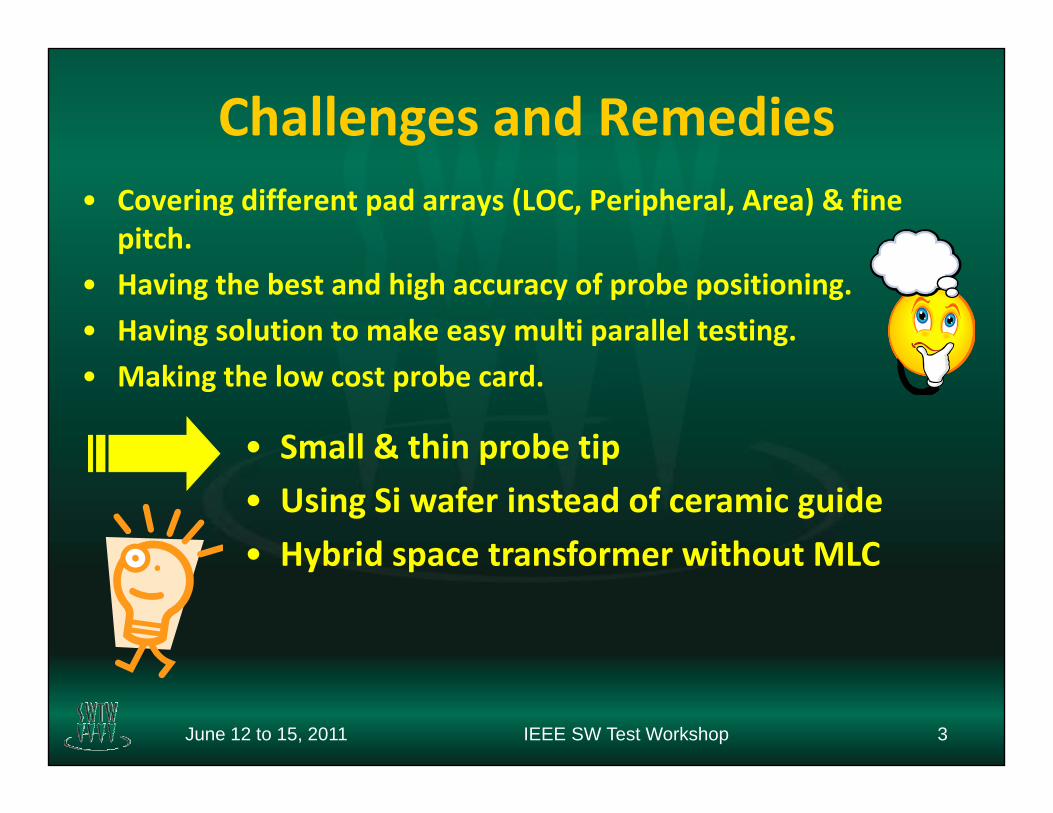
Probe Tip
Cantilever Vertical MEMS G‐probe
70um
Cantilever Vertical MEMS G probe
• G‐Probe is a vertical probe, made by electroforming• Planar 2D, Covers fine pitch‐ 20um pin thickness‐ Pitch, Inline : 40um, staggered : 20um, WLCSP : 130um
• Force‐ Cobra type : 5gf @ 70um travel‐ Spring type : 1gf @ 50um travel
• Good pointing accuracy by limited guideC b S i• Covers LOC, peripheral, area pad arrays
• Small scrub limited by MEMS guide
Cobra Spring

Test Equipment
Thru Cal kit(De‐embedding pattern)
T t HP 8510C V t N t k A l
GSG Probe
• Tester : HP 8510C Vector Network Analyzer• Test Jig : UTF (Universal Test Fixture)• Test pin : G‐probe Cobra type , 80um pitch• Pin array : GND‐Signal‐GND, GND‐Signal

Test Data
8
10
65
70
75m3freq=L=2.246
1.000GHz
m4
4
6
8
45
50
55
60
65
nduc
tanc
e [n
H]
Q-factor
m4
m4freq=Q=56.188
1.000GHz
L = 2.2nH
2 3 4 5 6 7 8 91 10
2
0
30
35
40
25
In m3
• Tip insertion loss (80um pitch, Probe Height: 2.93mm)GSG type : 1 1dB @1GHz
Frequency [GHz]
‐ GSG type : 1.1dB @1GHz‐ GS type : 0.9dB @1GHz
• G‐probe Model : 2.2nH High‐Q inductorG d f t til t (GH VS MH )• Good performance compare to cantilever type (GHz VS. MHz)

Probe Specification Thickness scatter
21~22um
19~20um20~21um
• Probe tip pointing accuracy : 0.5um• Probe thickness : 20um 1.0um (>90% within 8” area)M th 20K b ti ithi 8” i l t l ti• More than 20K probe tip within 8” area using electroplating process
• Low cost and easy fabrication process

Space TransformerPCB ST Wafer ST FPCB ST
2 Layer2 Layer2 Layer
1 Layer
2 Layer
1 Layer
• Hybrid space transformer constructionSi Wafer rigid PCB FPCB‐ Si Wafer, rigid PCB, FPCB
• Fine‐pattern process (width 10um, space 10um)•Multilayer, 10um small via processCTE t hi ith d i b f i Si f• CTE matching with device because of using Si wafer
• Low cost and fast delivery

G‐probe Example 1
• Application: Wide I/O Memory Bump• Device pitch, X:50um, Y:40um• Ball Bump Size : Ф 20umBall Bump Size : Ф 20um • 1‐PARA / 200 Probes• Probing pitch, X: 50um, Y:120um • Pointing accuracy: ± 3um, Planarity : ±2um

G‐probe Example 1
15
G‐probe Position Scatter & probing mark
6
9
12
‐3
0
3
Y error [um
]
Probing mark
‐9
‐6
‐3Y
‐15
‐12
‐15 ‐12 ‐9 ‐6 ‐3 0 3 6 9 12 15
X error [um]X error [um]

G‐probe Example 2
Probe blockRelay
Probe block
FrameR, L, C
Main PCB
a e
• Device : Media SOC• I/O Pad configuration : Peripheral in-line• I/O Pad configuration : Peripheral in line• Pad pitch : 50um• Probe block area : 50.72*20.57=1043.3mm2
• Pin count : 213x16=3408 probesb d i f d l l TM• Probe card interface : Teradyne UltraFlexTM
• Array :

G‐probe Example 24Para
Cantilever16ParaG‐probe
G‐probe wafer test Map
Test yield 79.9 % 80.0 %
Open fail 0.1% 0.1%
Logic 3.1% 3.2%
BIRA 2.2% 2.1%
Etc. 14.7% 14.6%
Shmoo for the BIST• Probe Card‐ 4Para Cantilever‐ 16Para G‐probe
• Measure yield & shmoo with same wafer• Better shmoo performance than cantilever S i ld• Same Test Yield

G‐probe Example 2
40
50
10
20
30m]
‐10
0
10
Y error[um
‐40
‐30
‐20
‐50‐50 ‐40 ‐30 ‐20 ‐10 0 10 20 30 40 50
X error[um]
• 3408 probes positioning error < ±10um

G‐probe Example 3
Interposer
Ref align blockUnit probe block(UPB)
Interposer
Main PCB
Space transformerProbe
Device wafer
p
Advantage of block array “G‐probe” probe card
• Easy repair & assembly
• Easy block array for the multi parallel test
• Good CTE matching by using Si wafer for making UPB & reference align block

G‐probe Example 3
40
50
10
20
30
m]
‐20
‐10
0
Y error[um
‐40
‐30
20
‐50‐50 ‐40 ‐30 ‐20 ‐10 0 10 20 30 40 50
X error[um]
9600 b i i i 0• 9600 probes positioning error < ±10um

G‐probe Example 3Temperature test at 90°C
B AAB
D C
CD
Probing area : 60,700um*121,400um Probe tip size : 15~18 um Pad size : 70um*70um 6 times touch down for 1hr at 90°C after initial probing (at room temp.) Good CTE matching

Summary• Novel vertical MEMS probe card
O t i t f t diti l ti l b d– Overcomes constraint of traditional vertical probe card• Fine pitch : Inline 40um, Staggered 20um, Area 130um• Pad array : LOC Peripheral Area (WLCSP)• Pad array : LOC, Peripheral, Area (WLCSP)
– MEMS guide• Good position accuracyp y• CTE matching with device wafer
– Hybrid space transformer• Low cost & fast delivery• CTE matching with MEMS probe block
Great multi parallelism solution
June 12 to 15, 2011 IEEE SW Test Workshop 19
– Great multi parallelism solution

g l 4g l 4g{tÇ~ lÉâ4g{tÇ~ lÉâ4
June 12 to 15, 2011 IEEE SW Test Workshop 20