Embed Size (px)
Citation preview
NUMERICAL COUPLING OF ELECTRIC CIRCUIT EQUATIONS
AND ENERGY-TRANSPORT MODELS FOR SEMICONDUCTORS∗
MARKUS BRUNK† AND ANSGAR JUNGEL†,‡
Abstract. A coupled semiconductor–circuit model including thermal effects is proposed. Thecharged particle flow in the semiconductor devices is described by the energy-transport equationsfor the electrons and the drift-diffusion equations for the holes. The electric circuit is modeled bythe network equations from modified nodal analysis. The coupling is realized by the node potentialsproviding the voltages applied to the semiconductor devices and the output device currents forthe network model. The resulting partial differential-algebraic system is discretized in time by the2-stage backward difference formula and in space by a mixed-hybrid finite-element method usingMarini-Pietra elements. A static condensation procedure is applied to the coupled system reducingthe number of unknowns. Numerical simulations of a one-dimensional pn-junction diode with time-depending voltage and of a rectifier circuit show the heating of the electrons which allows to identifyhot spots in the devices. Moreover, the choice of the boundary conditions for the electron densityand energy density is numerically discussed.
Key words. Energy-transport equations, circuit equations, semiconductor devices, modifiednodal analysis, mixed finite-element method, diode, Graetz bridge.
AMS subject classifications. 65L80, 65M60, 65N30, 82D37.
1. Introduction. In industrial applications, complex semiconductor devicemodels are usually substituted by circuits of basic network elements (resistors, capac-itors, inductors, voltage and current sources) resulting in simpler so-called compactmodels. Such a strategy was advantageous up to now since integrated circuit simula-tions were possible without computationally expensive device simulations. Parasiticeffects and high frequencies in the circuits, however, require to take into account avery large number of basic elements and to adjust carefully a large number of pa-rameters in order to achieve the required accuracy. Moreover, device heating and hotspots cannot be easily modeled by this approach.
Therefore, it is preferable to model those semiconductor devices which are criticalfor the parasitic effects by semiconductor transport equations. Since structural infor-mation about the resulting device–circuit equations was missing for a long time, thefirst approaches to couple circuits and devices were based on an extension of existingdevice simulators by more complex boundary conditions [35, 39] or the combinationof device simulators with circuit simulators as a “black box” solver [15]. Both ap-proaches, however, are not suitable for complex circuits in the high-frequency domain.In this work, we follow an approach that includes the device model into the networkequations directly. As the device model is described by partial differential equationsand the network equations are given by differential-algebraic equations (DAE), thisresults in a coupled system of partial differential-algebraic equations (PDAE).
The mathematical analysis and numerical approximation of coupled network and
∗The authors acknowledge partial support from the German Federal Ministry of Education andResearch (BMBF), grant 03JUNAVN, and from the bilateral DAAD-Vigoni Program. This researchis part of the ESF program “Global and geometrical aspects of nonlinear partial differential equations(GLOBAL)”. The authors thank Prof. Caren Tischendorf (University of Koln) and Dr. Uwe Feldmann(Qimonda, Munich) for fruitful discussions.
†Institut fur Mathematik, Universitat Mainz, Staudingerweg 9, 55099 Mainz, Germany; e-mail:brunk,[email protected].
‡Institut fur Analysis und Scientific Computing, Technische Universitat Wien, Wiedner Haupt-str. 8-10, 1040 Wien, Austria; e-mail: [email protected].
1

2 M. BRUNK AND A. JUNGEL
device equations were studied only recently. The first mathematical results wereobtained in [18, 20] where a semiconductor device was coupled to a simple circuit insuch a way that the currents entering the device can be expressed by a function ofthe applied voltage. In this case, the network is treated only as a special boundarycondition for the semiconductor. This approach fails for integrated circuits. A networkcontaining uniform lossy transmission lines was investigated in [21]. The resultingmodel becomes a PDAE system, but with partial differential equations of hyperbolictype. An electro-thermal problem coupling the network model with a heat equationcontaining a local dissipative power term was numerically solved in [4].
Later, networks with semiconductor devices described by the drift-diffusion equa-tions were studied. An existence analysis containing the drift-diffusion model wasdeveloped in [1, 2]. For a reliable and efficient numerical simulation, it is importantto know the index of the PDAE system consisting of the network and drift-diffusionequations. It has been shown in [46] that the coupled circuit is of (tractability) indexone if and only if the network(s) without the semiconductors satisfy some topologicalconditions, i.e., if they contain neither CV-loops nor LI-cutsets. Here, a loop con-sisting of capacitors and voltage sources only is called a CV-loop, whereas a cutsetcontaining inductors and current sources only is called an LI-cutset. In [47] it wasproved that the index of the coupled system is at most two under weak conditions onthe circuit (local passivity, no shortcuts). Moreover, the index of the coupled systemis two if and only if the circuit contains LI-cutsets or CVS-loops (loops of capacitors,voltage sources, and semiconductors) with at least one voltage source or one semicon-ductor device. The same results were obtained in [42] for the discretized drift-diffusionequations. A sensitivity analysis generalizing the DAE index for finite systems to infi-nite ones was presented in [7] and applied to the coupled PDAE system. It was shownthat the system is of index one if the voltages applied to the semiconductors are lowand the network without the semiconductors is of index one.
In this paper, we couple and simulate the network equations with the energy-transport model for semiconductors for the first time. Compared to the couplingwith the drift-diffusion equations, we are able to calculate the electron temperaturein the devices. The energy-transport model can be derived from the semiconductorBoltzmann equation in the diffusion limit under the assumption of dominant electron-electron scattering [5]. It consists of the conservation laws for the electron densityand the electron energy density with constitutive relations for the particle and energycurrent densities, coupled to the Poisson equation for the electric potential. Mathe-matically, the energy-transport equations (without the Poisson equation) constitutea parabolic cross-diffusion system in the entropic variables [14]. The system can bewritten in a drift-diffusion-type formulation, which allows for an efficient numericalapproximation [13].
The energy-transport model is discretized by mixed-hybrid finite elements ofMarini-Pietra type [32, 33]. The one-dimensional equations are considered in or-der to test the coupling and to achieve a fast algorithm required by our industrialpartner. For two-dimensional simulations of the energy-transport model (withoutany coupling to circuits), we refer to [23, 24]. Marini-Pietra finite elements instead ofstandard Raviart-Thomas elements are employed since this guarantees the M-matrixproperty of the global stiffness matrix, even in the presence of zeroth-order terms.Hence, the positivity of the particle densities is guaranteed. For the bipolar devicesconsidered in this paper, we model the flow of the positively charged holes by thedrift-diffusion equations which are also approximated by mixed Marini-Pietra finite
Numerical coupling of circuits and semiconductors 3
elements.The network equations as well as the parabolic equations are discretized in time by
the 2-stage backward difference formula (BDF2) since this scheme allows to maintainthe M-matrix property. Then, the semi-discretized equations are approximated by themixed finite-element method and static condensation is applied to reduce the numberof variables (see section 3 for details). The final nonlinear discrete system is solvedby Newton’s method.
For large applied bias, we observe strong gradients of the temperature at theboundary. Employing Robin boundary conditions for the electron density and en-ergy density instead of standard Dirichlet conditions allows to essentially eliminatethe boundary layer. This is the first time that the energy-transport equations arenumerically solved with Robin boundary conditions.
The paper is organized as follows. In section 2 we describe the circuit modelusing modified nodal analysis and the semiconductor device model employing theenergy-transport equations. Moreover, the coupling of both models is explained.Section 3 is devoted to the numerical discretization of the circuit and semiconductorequations. In section 4 two circuits containing one-dimensional semiconductor devicesare simulated, namely a pn-junction diode with time-depending applied voltage and arectifier circuit with four pn diodes. The numerical results from the transient energy-transport equations are compared with those from the stationary energy-transportmodel and from the transient drift-diffusion equations. Finally, we conclude in section5.
2. Modeling. In this section we explain the modeling of the electric circuits bymodified nodal analysis and of the semiconductor devices using the energy-transportand drift-diffusion equations. Furthermore, the coupling of both models is madeexplicit.
2.1. Circuit modeling. The circuits considered in this paper are supposed tocontain (ideal) resistors, capacitors, inductors, and voltage sources. In addition, weuse ideal current sources, as they appear in proper compact models for semiconductordevices. Thus we can reduce these electric circuits by RCL-circuits (just containingresistors, capacitors, and inductors).
A well-established mathematical description of RCL-circuits is the modified nodalanalysis. The basic tools are the Kirchhoff laws and the current-voltage characteristicsof the basic elements. In order to accomplish the modified nodal analysis, the circuit isreplaced by a directed graph with branches and nodes. Branch currents, branch volt-ages, and node potentials (without the mass node) are introduced as (time-dependent)variables. Then, the circuit can be characterized by the incidence matrix A = (ajk)describing the node-to-branch relations and defined as
ajk =
1 if the branch k leaves the node j,−1 if the branch k enters the node j,
0 else.
(see [48] for details on circuit topologies). The Kirchhoff current law expresses thatthe sum of all branch currents entering a node is equal to zero,
Ai = 0,
and the Kirchhoff voltage law means that the sum of all branch voltages in a loopvanishes, which can be expressed here as
v = A⊤e,
4 M. BRUNK AND A. JUNGEL
where i, v, and e are the vectors of branch currents, branch voltages, and nodepotentials, respectively. The current-voltage characteristics for the basic elementscan be given as
iR = g(vR), iC =dq
dt(vC), vL =
dΦ
dt(iL),
where g denotes the conductivity of the resistor, q the charge of the capacitor, andΦ the flux of the inductor. Moreover, iα and vα with α = R, C, L, are the branchcurrent vectors and branch voltage vectors for, respectively, all resistors, capacitors,and inductors. The network branches are numbered in such a way that the incidencematrix forms a block matrix with blocks describing the different types of networkelements, i.e., A consists of the block matrices AR, AC , AL, Ai, and Av, where theindex indicates the resistive, capacitive, inductive, current source, and voltage sourcebranches, respectively.
Denoting by is = is(t) and vs = vs(t) the given input functions for the currentand voltage sources, respectively, and replacing the branch currents in the Kirchhoffcurrent law by the current-voltage characteristics and the branch voltages by nodepotentials using the Kirchhoff voltage law, we obtain the system in the charge-orientedmodified nodal analysis approach [48],
ACdq
dt(A⊤
Ce) +ARg(A⊤
Re) +ALiL +Aviv = −Aiis, (2.1)
dΦ
dt(iL) −A⊤
Le = 0, (2.2)
A⊤
v e = vs (2.3)
for the unknowns e(t), iL(t), and iv(t). Equation (2.1) is the Kirchhoff current law forthe complete circuit, where the current-voltage relations for the resistors and capaci-tors have been included. Equation (2.2) decribes the voltage-current characteristic forthe inductors, and (2.3) determines the node potentials adjacent to the given voltagesources.
Equations (2.1)-(2.3) represent a system of differential-algebraic equations (DAE)with a properly stated leading term [30, 31] if the matrices C(v, t) = (∂q/∂v)(v, t)and L(i, t) = (∂Φ/∂i)(i, t) are positive definite for all arguments v, i, and t. Underthe assumptions that the matrices C, L, and G = ∂g/∂v are positive definite and thatthe circuit does neither contain loops of voltage sources only nor cutsets of currentsources only, it is proved in [46, 48] that the (tractability) index of the DAE system isat most two. Furthermore, if the circuit does neither contain LI-cutsets nor CV-loopswith at least one voltage source (see the introduction) then the index is at most one.
2.2. Semiconductor device modeling. In the semiconductor device, we as-sume that the electron flow can be described by the energy-transport equations. Theyconsist of the (scaled) conservation laws for the particle density n and energy densityw,
∂tn− divJn = −R(n, p), (2.4)
∂tw − divJw = −Jn · ∇V +W (n, T ) −3
2TR(n, p), (2.5)
together with (scaled) constitutive relations for the particle current Jn and energycurrent density Jw,
Jn = µn
(∇n−
n
T∇V
), Jw =
3
2µn(∇(nT ) − n∇V ), (2.6)
Numerical coupling of circuits and semiconductors 5
coupled self-consistently to the Poisson equation for the electric potential V ,
λ2∆V = n− p− C(x). (2.7)
Here, the electron temperature T is defined via the relation w = 32nT , p denotes the
hole density determined by the drift-diffusion equations
∂tp+ divJp = −R(n, p), Jp = −µp(∇p+ p∇V ), (2.8)
and the function C(x) models fixed charged background ions in the semiconductorcrystal (doping profile). The physical parameters are the (scaled) electron and holemobilities µn and µp and the Debye length λ, given by
λ2 =εsUT
qCmL,
where εs is the permittivity constant, UT = kBTL/q with the Boltzmann constant kB ,the lattice temperature TL and the elementary charge q denotes the thermal voltage,Cm is the maximal doping value, and L is the device diameter. The equations (2.4)-(2.8) are solved in the bounded domain Ω. The function
W (n, T ) = −3
2
n(T − TL)
τ0
with the (scaled) energy relaxation time τ0 and the lattice temperature TL = 1 de-scribes the energy relaxation to the equilibrium energy, and
R(n, p) =np− n2
i
τp(n+ ni) + τn(p+ ni)(2.9)
models recombination-generation processes with the (scaled) intrinsic density ni andthe material-depending electron and hole lifetimes τn and τp, respectively.
We have used the following scaling. The densities n, p, ni, and C are scaled bythe maximal doping concentration Cm = max |C(x)|; the temperature is scaled bythe lattice temperature (usually, 300 K); the electric potential by the thermal voltageUT ; the mobilities µn and µp by µ = maxµn, µp; and finally, the relaxation time τ0and the lifetimes τn, τp by t0 = L2/(UT µ). For notational convenience, we have notrenamed the scaled quantities.
For the model equations (2.4)-(2.8) we need to impose appropriate initial andboundary conditions. We prescribe the initial conditions for the particle densities andthe temperature
n(·, 0) = nI , p(·, 0) = pI , T (·, 0) = TI on ∂Ω. (2.10)
The device boundary is assumed to split into two parts, the union of Ohmic contactsΓD and the union of insulating boundary segments ΓN , where ∂Ω = ΓD ∪ ΓN . Al-though we will present later spatial one-dimensional simulations, we give the boundaryconditions for the multidimensional situation. On the insulating parts, it is assumedthat the normal components of the current densities and of the electric field vanish,
Jn · ν = Jp · ν = Jw · ν = ∇V · ν = 0 on ΓN , t > 0. (2.11)
6 M. BRUNK AND A. JUNGEL
At the contacts, the temperature, the electric potential, and the particle densities areassumed to be known. The electric potential equals the sum of the applied voltage Uand the so-called built-in potential Vbi,
V = U + Vbi on ΓD, t > 0. (2.12)
The built-in potential is the potential in the device in thermal equilibrium,
Vbi = arsinh( C
2ni
).
The temperature is supposed to be equal to the (scaled) lattice temperature at thecontacts:
T = 1 on ΓD, t > 0. (2.13)
The boundary conditions for the particle densities are derived under the assumptionsof charge neutrality, n − p − C(x) = 0, and thermal equilibrium, np = n2
i . Solvingthese equations for n and p gives
n =1
2
(C +
√C2 + 4n2
i
), p =
1
2
(− C +
√C2 + 4n2
i
)on ΓD. (2.14)
We will show in section 4 that the Dirichlet boundary conditions for the particledensities and the temperature may lead, for large applied voltages, to strong boundarylayers. Therefore, we will also employ Robin boundary conditions for comparison (seesection 4).
Energy-transport models have been used by engineers for more than 40 years todescribe thermal effects in semiconductor devices [44], mostly with phenomenologicaltransport coefficients. In the physical literature, these models have been usuallyderived from hydrodynamic equations by neglecting certain convection terms (see [40]and references therein). Another approach is to derive the energy-transport modelsfrom the semiconductor Boltzmann equation by using a Hilbert expansion methodunder the assumptions of nondegenerate Boltzmann statistics and dominant electron-electron and elastic collisions [5]. Depending on the conditions on the microscopicrelaxation time, various energy-transport models can be derived [13]. Here, we employthe model of [11] which is also used in the simulations of [23, 24].
The numerical discretization of energy-transport models has been investigated inthe physical literature for quite some time [11, 16, 43]. Mathematicians started topay attention to these models in the 1990s, using essentially non-oscillatory (ENO)schemes [25], finite-difference methods [17, 38], mixed finite-volume schemes [8], ormixed finite-element methods [23, 24, 27, 34] (also see [10] for an overview).
In this paper, we will use as in [13] the mixed finite-element method applied tothe drift-diffusion-like formulation of the energy-transport model since this methodallows for a good approximation of the current densities (see, e.g. [3, 10]). For this,we define the variables g1 = µnn and g2 = 3
2µnnT and write (2.4)-(2.6) as
µ−1n ∂tg1 − divJn = −R(n, p),
µ−1n ∂tg2 − divJw = −Jn · ∇V +W (n, T ) −
3
2TR(n, p)
with the current densities
Jn = ∇g1 −g1T∇V, Jw = ∇g2 −
g2T∇V, (2.15)
Numerical coupling of circuits and semiconductors 7
where the temperature is now given by T = 2g2/3g1. This corresponds (up to a sign)to the drift-diffusion equations (2.8), where p is replaced by g1 or g2, T = 1, and theright-hand side is different. The initial and boundary conditions for g1, g2, and Vnow follow directly from (2.10)-(2.14).
2.3. Coupling. The coupling is realized on the one hand by the semiconductorcurrent density from the energy-transport and drift-diffusion equations, which needsto be included in the Kirchhoff current law (2.1), and on the other hand by thepotentials of the circuit nodes adjacent to the semiconductor device, defining theboundary condition for the electric potential in the device.
First, we consider the semiconductor current density which consists of three parts,the electron current Jn, the hole current Jp, and the displacement current Jd causedby the electric potential and given by Jd = −λ2∂t∇V . The total current density Jtot
is then given by
Jtot = Jn + Jp + Jd.
The displacement current guarantees charge conservation. Indeed, differentiating thePoisson equation (2.7) with respect to time and replacing the time derivatives of theparticle densities by (2.4) and (2.8), we obtain
divJtot = div(Jn + Jp) − ∂t(n− p) = 0.
The current leaving the semiconductor device at terminal k, corresponding to theDirichlet boundary part Γk, is defined by
jk =
∫
Γk
Jtot · ν ds.
Clearly, due to charge conservation, the current through one terminal can be computedby the negative sum of the currents through all other terminals. Therefore, it ispossible to choose one terminal (usually the bulk terminal) as the reference terminal.We denote by jS the vector of all terminal currents except the current corresponding tothe reference terminal. In the one-dimensional case, there remains only one terminal,and the current through the terminal at x = 0 is given by
jS(t) = Jn(0, t) + Jp(0, t) − λ2∂tVx(0, t).
Now, we define the semiconductor incidence matrix AS by its elements
aik =
1 if the current jk enters the circuit node i,−1 if the reference terminal is connected to the node i,
0 else.
Including the row for the mass node, each column of AS has exactly one entry 1and one entry −1. Therefore, it is of the same form as the other incidence matricesintroduced in section 2.1 and can be added to the Kirchhoff current law (2.1), leadingto
ACdq
dt(A⊤
Ce) +ARg(A⊤
Re) +ALiL +Aviv +ASjS = −Aiis.
Notice that this procedure extends easily to the case of several semiconductors. Inthis situation, we need to choose one reference terminal for each semiconductor device
8 M. BRUNK AND A. JUNGEL
and to follow the above procedure for each device. We notice that the scaling of timein the semiconductor model also changes the time variable in the above DAE system,for instance t = t0ts, where t0 is the scaling factor and ts is the scaled time, and thetime derivative d/dt has to be replaced by t−1
0 (d/dts).The second part of the coupling is described via the boundary conditions for the
electric potential in the semiconductor device. On the terminal k, we have
V (t) = ei(t) + Vbi on Γk,
if the terminal k of the device is connected to the circuit node i, where ei denotes thepotential at the circuit node i.
We summarize the complete coupled system with one-dimensional semiconductorequations. The network equations are given by
ACdq
dt(A⊤
Ce) +ARg(A⊤
Re) +ALiL +Aviv +ASjS = −Aiis,
dΦ
dt(iL) −A⊤
Le = 0,
A⊤
v e = vs,
the current jS is defined by
jd,S − λ2Vx = 0, jS − (Jn + Jp − ∂tjd,S) = 0, (2.16)
the semiconductor model reads as
µ−1n ∂tg1 − Jn,x = −R, λ2Vxx = µ−1
n g1 − p− C(x),
µ−1n ∂tg2 − Jw,x = −JnVx +W −
3
2TR, ∂tp+ Jp,x = −R,
together with the current relations
Jn = g1,x −g1TVx, Jw = g2,x −
g2TVx, Jp = −µp (px + pVx) .
The boundary conditions for the potential are
V (0, t) = ei + Vbi(0), V (1, t) = ej + Vbi(1)
for appropriate nodes ei and ej . The remaining boundary conditions for g1, g2, andT are given by
n(x, t) =1
2
(C(x) +
√C(x)2 + 4n2
i
), T (x, t) = TL,
p(x, t) =1
2
(− C(x) +
√C(x)2 + 4n2
i
)at x = 0, 1.
For the choice of initial conditions, we refer to section 4.The equations above form a system of partial differential-algebraic equations.
We have already mentioned in the introduction that the partial differential-algebraicequations resulting from a coupled circuit with the drift-diffusion equations have atmost index 2 and that they have index 1 under some topological assumptions [6, 47].No analytical result is available for the coupled system consisting of the circuit andenergy-transport equations. However, we conjecture that the index of this system isalso at most two.

Numerical coupling of circuits and semiconductors 9
3. Numerical approximation.
3.1. Numerical integration of DAEs. For the numerical integration of diffe-rential-algebraic equations (DAEs) we can employ Runge-Kutta methods or backwarddifference formulas (BDF). For Runge-Kutta methods applied to DAEs we refer to[22], for instance. Only implicit Runge-Kutta schemes are feasible for DAEs, andstiffly accurate methods provide the best properties. For instance, stiffly accuratemethods for index-1 DAEs have the same convergence order as in the case of thenumerical integration of explicit ordinary differential equations. For other Runge-Kutta methods, order reduction in the algebraic part down to the stage order q occurs.For stiffly accurate methods for index-2 DAEs, an order reduction in the differentialand algebraic part down to the order q+ 1 can be observed. For other methods, evenstronger order reduction may occur.
Concerning BDF methods, k-step BDF (with k < 7) for index-1 DAEs are feasiblefor sufficiently small time steps, and they are convergent with the same order as inthe case of explicit ordinary differential equations [29]. The numerical integrationof index-2 DAEs with BDF is studied in [9, 22]. In [45], quasilinear index-2 DAEs,as they occur in circuit simulation, were examined. It has been shown that k-stepBDF for k < 7 are feasible and weakly instable under suitable assumptions. Theconvergence order is the same as in the case of explicit ordinary differential equations.
In the previous subsection, we made the conjecture, based on coupled drift-diffusion and network equations, that the index of the partial differential-algebraicsystem derived in section 2.3 is not larger than two. Therefore, we employ the 2-stepBDF, defined by
∂tg(tm) ≈1
2t(3g(m+1) − 4g(m) + g(m−1)), (3.1)
where g(k) approximates g(·, tk), tk = kt. We found that on the one hand, simplemethods like the implicit Euler scheme have a too strong damping effect. On theother hand, methods like Radau IIa are not suitable since the stiffness matrix comingfrom the finite-element discretization of the semiconductor equations does not pro-vide an M-matrix after static condensation (see below for details). Using the 2-stepBDF allows to keep the M-matrix property provided by the finite-element scheme.Furthermore, higher-order schemes are not appropriate here, since the input signalsmay be discontinuous.
3.2. Numerical discretization of the energy-transport equations. Thesemiconductor equations are discretized in time by the 2-step BDF (see section 3.1)and in space by a mixed-hybrid finite-element scheme. The Poisson equation is dis-cretized by a standard P1 finite-element method. Thus, the discrete electric potentialis piecewise linear and the approximation of the electric field −Vx is piecewise con-stant. In the following we only describe the discretization of the electron and energyequation, since the discretization of the hole equation is similar.
The recombination-generation term (2.9) is treated semi-linearly. More precisely,we employ in the denominator the values of the particle densities from the former timestep, whereas in the enumerator, one of the particle densities is fixed (using again thevalues of the previous time step). In this way, the recombination-generation term
becomes, in each iteration step, linear. For given V , T , and p and g1 and Jn from theprevious time step, we can thus express the continuity equations as
µ−1n ∂tgj − Jj,x + σjgj = fj , j = 1, 2,
10 M. BRUNK AND A. JUNGEL
where the current densities J1 = Jn and J2 = Jw are given by (2.15) and
σ1 =µ−1
n p
τp(µ−1n g1 + ni) + τn(p+ ni)
, σ2 =3
2T σ1 + (µnτ0)
−1,
f1 =n2
i
τp(µ−1n g1 + ni) + τn(p+ ni)
, f2 =3
2T f1 − JnVx +
3
2(µnτ0)
−1TLg1.
After time discretization with the 2-step BDF (3.1) we obtain at time tm+1 =(m+ 1)t
−Jj,x + σjgj = fj , Jj = gj,x −gj
TVx, j = 1, 2, (3.2)
where
σj = σj +3
2(µnt)
−1gj , fj = fj + 2(µnt)−1g
(m)j −
1
2(µnt)
−1g(m−1)j
and g(m)j and g
(m−1)j are the values of gj from the previous time steps.
In the following we explain the spatial discretization of (3.2) using mixed finiteelements. In the case σj = 0, the use of the lowest-order Raviart-Thomas elements[37] guarantees that the resulting stiffness matrix is an M-matrix. This provides apositivity-preserving numerical scheme, i.e., the discrete particle densities stay posi-tive if they are positive initially and on the boundary. Unfortunately, this propertygenerally does not hold in the presence of the zeroth-order term σigi. Marini andPietra [33] have developed finite elements which guarantee the M-matrix propertyeven with zeroth-order terms. They have been successfully applied to the energy-transport equations in one and two space dimensions [13, 23, 24].
We consider (3.2) in the interval (0, 1) with Dirichlet boundary conditions (seesection 2.3) and with Robin boundary conditions (see section 4). For convenience,we omit the index j in (3.2). We introduce the uniform mesh xi = ih, i = 0, . . . , N ,where N ∈ N and h = 1/N . In order to deal with the convection dominance dueto high electric fields, we use exponential fitting. Assume in the following that thetemperature is given by a piecewise constant function T (see (3.6) for the definition ofT ) and that the electric potential V is a given piecewise linear function. Then we definea local Slotboom variable by y = exp(−V/T )g in each subinterval Ii = (xi−1, xi).Equation (3.2) can be written as
e−V/TJ − yx = 0, −Jx + σeV/T y = f.
The ansatz space for the current density J consists of piecewise polynomials ofthe form ψi(x) = ai + biPi(x) on each Ii with constants ai, bi and second-orderpolynomials Pi(x) which are defined as follows. Let P (x) be the unique second-order
polynomial satisfying∫ 1
0P (x)dx = 0, P (0) = 0, and P (1) = 1. Then P (x) = 3x2−2x.
We define Pi(x) (depending on V ) by
Pi(x) = −P(xi − x
h
)for imin = i− 1,
Pi(x) = P(x− xi−1
h
)for imin = i,
where imin is the boundary node of Ii at which the potential attains its minimum.Notice that the minimum is always attained at the boundary since V is linear on Ii.If V is constant in Ii, we define Pi(x) = P ((x− xi−1)/h).
Numerical coupling of circuits and semiconductors 11
Now we introduce the finite-dimensional spaces:
Vh = ψ ∈ L2(0, 1) : ψ(x) = ai + biPi(x) in Ii, i = 1, . . . , N,
Wh = φ ∈ L2(0, 1) : φ is constant in Ii, i = 1, . . . , N,
Γh,ξ = q is defined at the nodes x0, . . . , xN , q(x0) = ξ(0), q(xN ) = ξ(1).
The mixed-hybrid finite-element approximation of (3.2) is as follows. Find Jh ∈ Vh,gh ∈Wh, and gh ∈ Γh,gD
such that
N∑
i=1
( ∫
Ii
QiJhψdx+
∫
Ii
Sighψxdx−[e−V/T ighψ
]xi
xi−1
)= 0, (3.3)
N∑
i=1
(−
∫
Ii
Jh,xφdx+
∫
Ii
σghφdx)
=
N∑
i=1
∫
Ii
fφdx, (3.4)
N∑
i=1
[qJh
]xi
xi−1= 0 (3.5)
for all ψ ∈ Vh, φ ∈Wh, and q ∈ Γh,0, where gD denotes the Dirichlet boundary valuesof g, and
Qi =1
h
∫
Ii
e−V (x)/T idx, Si = e−Vmin/T i , i = 1, . . . , N,
are introduced in order to treat accurately large gradients of the potential [33]. Here,Vmin denotes the minimal value of V on Ii. Equation (3.3) is the weak formulation ofthe second equation in (3.2), together with the inverse of the Slotboom transformation.Notice that the discrete inverse transformation is not the same for the variables gh
and gh. Equation (3.4) is the discrete weak version of the first equation in (3.2). Thethird equation (3.5) implies the continuity of Jh at the nodes. Clearly, in the case ofRobin boundary conditions, these equations have to be modified appropriately.
The additional variables Jh and gh can be eliminated by static condensation. Forthis, we write the weak formulation in matrix-vector notation for the vectors of nodalvalues similarly as in [23]:
A B⊤ −C⊤
−B D 0C 0 0
Jh
gh
gh
=
0F0
.
The matrices A ∈ R2N×2N , B ∈ R
N×2N , C ∈ R(N−1)×2N , and D ∈ R
N×N are givenby the corresponding elementary matrices associated with the interval Ii, denoted bythe superscript i:
Aijk = Qi
∫
Ii
ψjψkdx, Bijk =
∫
Ii
φjψk,xdx,
Cijk =
[qjψk
]xi
xi−1, Di
jk =
∫
Ii
σφjφkdx,
where ψk, φk, and qk are the canonical basis functions of the corresponding spaces.Furthermore, the matrices B and C are given by the elementary matrices
Bi = SiBi, Ci
jk =[e−Vj/T iqjψk
]xi
xi−1,
12 M. BRUNK AND A. JUNGEL
and the right-hand side F represents the integral on the right-hand side of (3.4).Now, static condensation as in [23] can be applied. As the matrix A has a diagonal
structure, it can be easily inverted, which allows to eliminate Jh. A similar argumentfor BA−1B⊤ +D allows to eliminate gh. This leads to the system
Mgh = G.
The stiffness matrix M has a tridiagonal structure with diagonal elements
Mii =1
h
(Ni+1+
Vi+1 − Vi
2T i+1
+Ni−Vi − Vi−1
2T i
)+
hσi
γiσi + 1Pi(xi)−
hσi+1
γi+1σi+1 + 1Pi+1(xi),
where
Ni =Vi − Vi−1
2T i
cothVi − Vi−1
2T i
, γi =2
15h2Qie
Vmin/T i ,
Vi = V (xi), σi is the restriction of the piecewise constant function σ to Ii, and theelements on the secondary diagonals are
Mi,i+1 =1
h
(−Ni+1 +
Vi+1 − Vi
2T i+1
), Mi+1,i =
1
h
(−Ni −
Vi − Vi−1
2T i
).
It is not difficult to see that M is an M-matrix. In particular, it holds Mij ≤ 0 forall i 6= j. In view of the construction of the polynomial Pi, it holds either Pi(xi) = 1and Pi(xi−1) = 0 or Pi(xi) = 0 and Pi(xi−1) = −1. Thus Mii ≥ 0.
The components of the vector G are given by
Gi =hfi
γiσi + 1Pi(xi) −
hfi+1
γi+1σi+1 + 1Pi+1(xi+1),
where fi denotes the restriction of the piecewise constant function f (see (3.4)) toIi. Thus, for nonnegative f , also G is nonnegative. Since M is an M-matrix, thisshows the nonnegativity of the solution. For the equation for the particle densities, anonnegative right-hand side f can be achieved by adjusting the size of the time step.We cannot guarantee generally nonnegativity of the right-hand side for the energyequation since the term −JnVx may be negative and large. However, we observedthat −JnVx is negative in few cases only, and by adjusting the step size in space andtime we always obtained positive solutions even for negative values of the right-handside.
The eliminated variables gh and Jh can be computed by the following relations:
gih =
1
γiσi + 1(gimin
h + γifi),
J ih = Ni
gih − gi−1
h
h−gi
h + gi−1h
2T i
Vi − Vi−1
2T i
+h
γiσi + 1(gimin
h σi − fi)Pi(x).
In order to complete the scheme, we still have to specify how the piecewise con-stant temperature T is defined. The temperature is implicitly defined in terms of g1and g2, T = 2g2/3g1. Hence, we define
T i =1
2(Ti + Ti−1), where Ti =
2gi2,h
3gi1,h
. (3.6)

Numerical coupling of circuits and semiconductors 13
Parameter Physical meaning Numerical valueLy extension of device in y-direction 6 · 10−7 mLz extension in z-direction 10−6 mq elementary charge 1.6 · 10−19 Asǫs permittivity constant 10−12 As/VcmUT thermal voltage at TL = 300K 0.026 Vµn/µp low-field carrier mobilities 1500/450 cm2/Vsτn/τp carrier lifetimes 10−6/10−5 sni intrinsic density 1016 m−3
τ0 energy relaxation time 4 · 10−13 sTable 4.1
Physical parameters for a silicon pn-junction diode.
For each time step, we have to solve a discrete nonlinear system correspondingto the discretized semiconductor equations and the network model. The Newtonmethod is applied to the whole system. The temperature is updated during theNewton iterations only if
‖(g1,h, g2,h, ph, Vh)new − (g1,h, g2,h, ph, Vh)old‖2 ≤ maxε, c‖T new − T‖d2,
where the parameters ε = 10−7, c = 0.01, and d = 0.08 are chosen similarly as in [23].For the first time step we apply the implicit Euler method (BDF1).
4. Numerical examples. In this section, we present the numerical results oftwo coupled circuit-semiconductor models, a pn-junction diode with time-dependingvoltage and a rectifier circuit (Graetz bridge) with four pn diodes.
4.1. A pn diode with time-depending voltage. We consider a silicon pn-junction with a time-depending voltage source. The diode is assumed to be homoge-neous in the y- and the z-direction such that a one-dimensional approach is suitable.In order to unscale the current densities and to obtain a current (and not a currentdensity), the size of the diode in the y- and z-direction are specified (see Table 4.1).The quasi one-dimensional diode consists of a p-doped region with length L/2 andminimal doping profile −C0 and of a n-doped region with the same length and witha maximal doping of C0. We have used the values L = 0.1µm or L = 0.6µm andC0 = 1022 m−3 or C0 = 5 · 1023 m−3, respectively. The doping profile is slightlysmoothed using the tanh function (see, e.g. [26]). The circuit operates with 1 GHz,i.e., the applied voltage equals v(t) = U0 sin(2πωt) with maximal voltage U0 = 1.5 Vand frequency ω = 109 Hz. The physical parameters are collected in Table 4.1. Werefer to [41] for more details about carrier life-times.
We have used a uniform spatial grid with 101 nodes and a uniform time stept = 10−13 s. The time step is rather small; this can be explained by the fact thatwe need careful computations at the switching point when the voltage changes fromforward to backward bias and vice versa. An adaptive time stepping procedure wouldcertainly allow to choose larger time steps; we plan to implement this in the future.
Initially, the semiconductor device is assumed to be in thermal equilibrium, i.e.,the total current of electrons and holes vanishes. Thus, the initial node potentials andthe current densities are taken to be zero. The initial displacement current is thendefined by jd,S(·, 0) = λ2(Veq)x, where Veq denotes the thermal equilibrium potential
14 M. BRUNK AND A. JUNGEL
given by
λ2(Veq)xx = e−Veq − eVeq − C(x), Veq(0, ·) = Vbi(0), Veq(1, ·) = Vbi(1).
Recall that Vbi is the built-in potential introduced in section 2.3. The definition ofjd,S ensures that the first equation in (2.16) is fulfilled. Summarizing, the initialconditions read as follows:
e = 0, iV = 0, jS = 0, jd,S = λ2(Veq)x,g1 = µnneq, g2 = 3
2µnneq, p = peq, V = Veq, T = 1,
where neq = e−Veq and peq = eVeq are the thermal equilibrium particle densities. Acomputation shows that the initial conditions are consistent for the coupled systemof PDAEs according to [28].
00.5
1
0
0.05
0.10
2
4
6
8
10x 10
21
time [ns]position [µm]
ener
gy d
ensi
ty [e
Vm
−3 ]
00.5
1
0
0.05
0.10
1
2
3
4x 10
23
time [ns]position [µm]
ener
gy d
ensi
ty [e
Vm
−3 ]
0
0.5
1
0
0.2
0.4
0
1
2
3x 10
21
time [ns]position [µm]
ener
gy d
ensi
ty [e
Vm
−3 ]
00.5
1
0
0.50
5
10
15x 10
22
time [ns]position [µm]
ener
gy d
ensi
ty [e
Vm
−3 ]
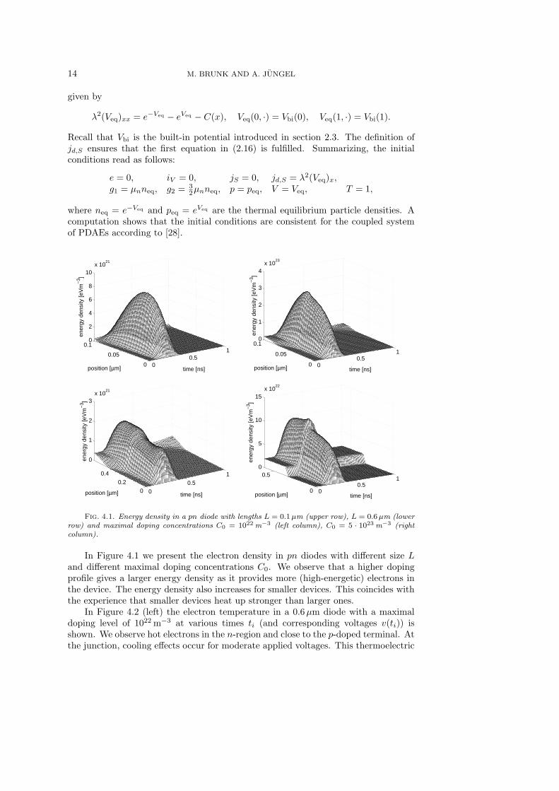
Fig. 4.1. Energy density in a pn diode with lengths L = 0.1 µm (upper row), L = 0.6 µm (lowerrow) and maximal doping concentrations C0 = 1022 m−3 (left column), C0 = 5 · 1023 m−3 (rightcolumn).
In Figure 4.1 we present the electron density in pn diodes with different size Land different maximal doping concentrations C0. We observe that a higher dopingprofile gives a larger energy density as it provides more (high-energetic) electrons inthe device. The energy density also increases for smaller devices. This coincides withthe experience that smaller devices heat up stronger than larger ones.
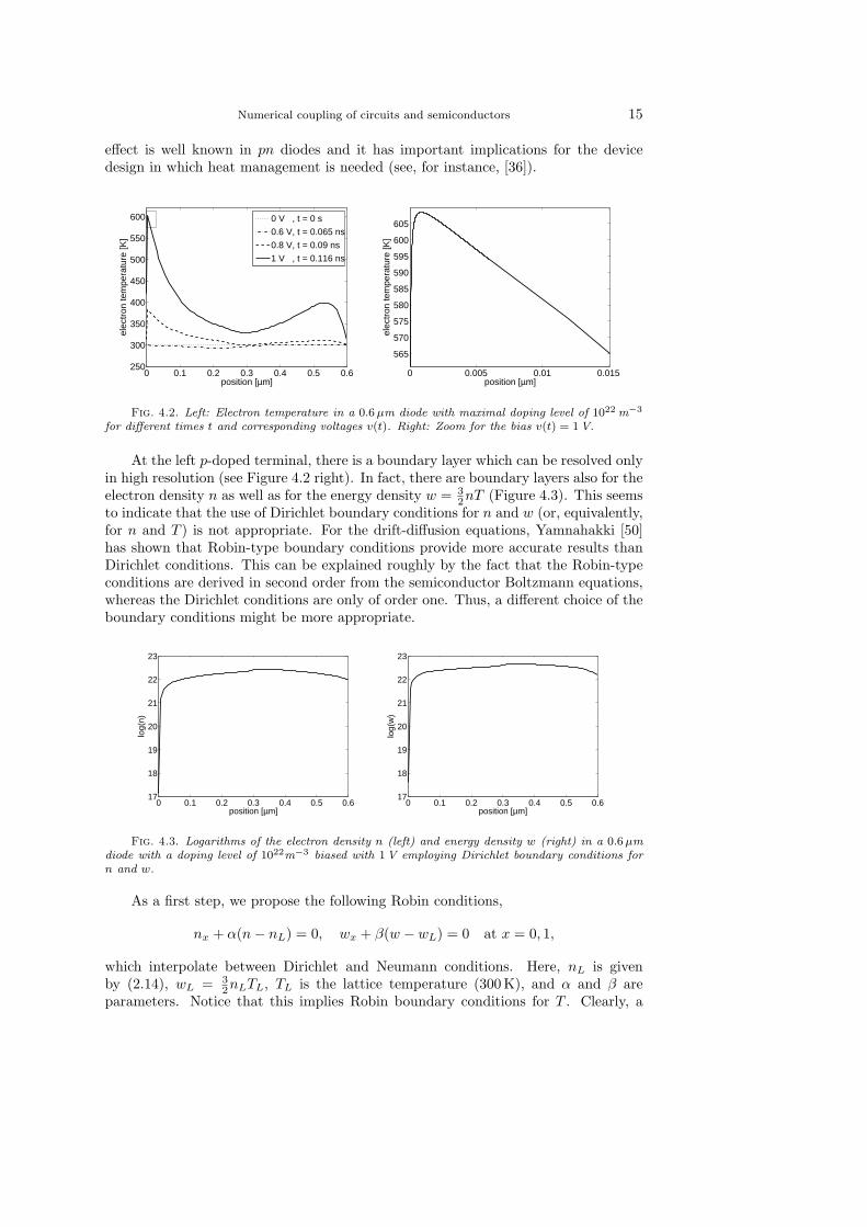
In Figure 4.2 (left) the electron temperature in a 0.6µm diode with a maximaldoping level of 1022 m−3 at various times ti (and corresponding voltages v(ti)) isshown. We observe hot electrons in the n-region and close to the p-doped terminal. Atthe junction, cooling effects occur for moderate applied voltages. This thermoelectric
Numerical coupling of circuits and semiconductors 15
effect is well known in pn diodes and it has important implications for the devicedesign in which heat management is needed (see, for instance, [36]).
0 0.1 0.2 0.3 0.4 0.5 0.6250
300
350
400
450
500
550
600
position [µm]
elec
tron
tem
pera
ture
[K]
0 V , t = 0 s
0.6 V, t = 0.065 ns
0.8 V, t = 0.09 ns
1 V , t = 0.116 ns
0 0.005 0.01 0.015
565
570
575
580
585
590
595
600
605
position [µm]el
ectr
on te
mpe
ratu
re [K
]
Fig. 4.2. Left: Electron temperature in a 0.6 µm diode with maximal doping level of 1022 m−3
for different times t and corresponding voltages v(t). Right: Zoom for the bias v(t) = 1V.
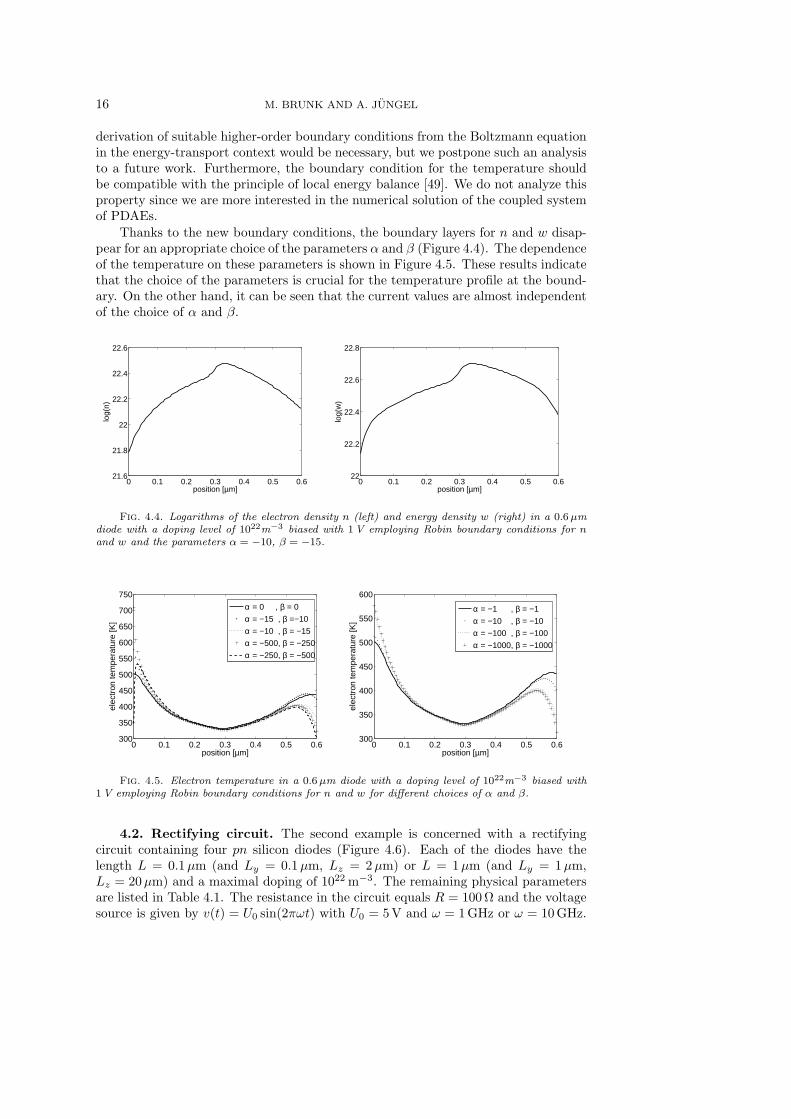
At the left p-doped terminal, there is a boundary layer which can be resolved onlyin high resolution (see Figure 4.2 right). In fact, there are boundary layers also for theelectron density n as well as for the energy density w = 3
2nT (Figure 4.3). This seemsto indicate that the use of Dirichlet boundary conditions for n and w (or, equivalently,for n and T ) is not appropriate. For the drift-diffusion equations, Yamnahakki [50]has shown that Robin-type boundary conditions provide more accurate results thanDirichlet conditions. This can be explained roughly by the fact that the Robin-typeconditions are derived in second order from the semiconductor Boltzmann equations,whereas the Dirichlet conditions are only of order one. Thus, a different choice of theboundary conditions might be more appropriate.
0 0.1 0.2 0.3 0.4 0.5 0.617
18
19
20
21
22
23
position [µm]
log(
n)
0 0.1 0.2 0.3 0.4 0.5 0.617
18
19
20
21
22
23
position [µm]
log(
w)
Fig. 4.3. Logarithms of the electron density n (left) and energy density w (right) in a 0.6 µmdiode with a doping level of 1022m−3 biased with 1V employing Dirichlet boundary conditions forn and w.
As a first step, we propose the following Robin conditions,
nx + α(n− nL) = 0, wx + β(w − wL) = 0 at x = 0, 1,
which interpolate between Dirichlet and Neumann conditions. Here, nL is givenby (2.14), wL = 3
2nLTL, TL is the lattice temperature (300 K), and α and β areparameters. Notice that this implies Robin boundary conditions for T . Clearly, a
16 M. BRUNK AND A. JUNGEL
derivation of suitable higher-order boundary conditions from the Boltzmann equationin the energy-transport context would be necessary, but we postpone such an analysisto a future work. Furthermore, the boundary condition for the temperature shouldbe compatible with the principle of local energy balance [49]. We do not analyze thisproperty since we are more interested in the numerical solution of the coupled systemof PDAEs.
Thanks to the new boundary conditions, the boundary layers for n and w disap-pear for an appropriate choice of the parameters α and β (Figure 4.4). The dependenceof the temperature on these parameters is shown in Figure 4.5. These results indicatethat the choice of the parameters is crucial for the temperature profile at the bound-ary. On the other hand, it can be seen that the current values are almost independentof the choice of α and β.
0 0.1 0.2 0.3 0.4 0.5 0.621.6
21.8
22
22.2
22.4
22.6
position [µm]
log(
n)
0 0.1 0.2 0.3 0.4 0.5 0.622
22.2
22.4
22.6
22.8
position [µm]
log(
w)
Fig. 4.4. Logarithms of the electron density n (left) and energy density w (right) in a 0.6 µmdiode with a doping level of 1022m−3 biased with 1V employing Robin boundary conditions for nand w and the parameters α = −10, β = −15.
0 0.1 0.2 0.3 0.4 0.5 0.6300
350
400
450
500
550
600
650
700
750
position [µm]
elec
tron
tem
pera
ture
[K]
α = 0 , β = 0
α = −15 , β =−10
α = −10 , β = −15
α = −500, β = −250
α = −250, β = −500
0 0.1 0.2 0.3 0.4 0.5 0.6300
350
400
450
500
550
600
position [µm]
elec
tron
tem
pera
ture
[K]
α = −1 , β = −1
α = −10 , β = −10
α = −100 , β = −100
α = −1000, β = −1000
Fig. 4.5. Electron temperature in a 0.6 µm diode with a doping level of 1022m−3 biased with1V employing Robin boundary conditions for n and w for different choices of α and β.
4.2. Rectifying circuit. The second example is concerned with a rectifyingcircuit containing four pn silicon diodes (Figure 4.6). Each of the diodes have thelength L = 0.1µm (and Ly = 0.1µm, Lz = 2µm) or L = 1µm (and Ly = 1µm,Lz = 20µm) and a maximal doping of 1022 m−3. The remaining physical parametersare listed in Table 4.1. The resistance in the circuit equals R = 100Ω and the voltagesource is given by v(t) = U0 sin(2πωt) with U0 = 5V and ω = 1GHz or ω = 10GHz.
Numerical coupling of circuits and semiconductors 17
h/L RE(n) RE(w) RE(p) RE(V ) RE(T ) RE(jS) RE(circuit)
0.04 8.7 · 10−2 1.3 · 10−1 6.8 · 10−2 2.3 · 10−2 1.0 · 10−1 1.1 · 10−1 1.5 · 10−2
0.02 3.5 · 10−2 5.3 · 10−2 2.7 · 10−2 1.2 · 10−2 7.3 · 10−2 5.0 · 10−2 6.9 · 10−3
0.01 1.1 · 10−2 1.7 · 10−2 8.0 · 10−3 4.1 · 10−3 4.7 · 10−2 1.7 · 10−2 2.3 · 10−3
0.005 2.4 · 10−3 3.9 · 10−3 1.8 · 10−3 1.1 · 10−3 2.3 · 10−2 4.1 · 10−3 5.7 · 10−4
rate 1.73 1.67 1.75 1.47 0.72 1.60 1.59Table 4.2
Relative error (RE) for different space step sizes. The time step size is t = 10−12s.
t RE(n) RE(ǫ) RE(p) RE(V ) RE(T ) RE(jS) RE(circuit)
10 2.0 · 10−3 1.6 · 10−3 1.9 · 10−3 6.0 · 10−4 5.6 · 10−3 2.1 · 10−3 3.6 · 10−4
8 1.5 · 10−3 1.1 · 10−3 1.4 · 10−3 5.2 · 10−4 4.5 · 10−3 1.6 · 10−3 3.0 · 10−4
5 7.3 · 10−4 5.7 · 10−4 6.8 · 10−4 3.5 · 10−4 2.8 · 10−3 1.5 · 10−3 2.2 · 10−4
4 5.5 · 10−4 4.1 · 10−4 5.1 · 10−4 3.1 · 10−4 2.7 · 10−3 1.4 · 10−3 1.8 · 10−4
rate 1.38 1.51 1.41 0.66 0.76 0.56 0.74Table 4.3
Relative error (RE) for different time step sizes. The space step size is h = 0.0025L; t ismeasured in units of 10−13 s.
We use the same initial conditions as in the previous subsection. For the Graetzbridge, we may employ Dirichlet or Robin boundary conditions as these conditionseffect the behavior of the temperature on the boundary but less the current values.Only the profile of the electron density changes slightly. Here, for simplicity, we haveemployed Robin conditions with large values for α and β, which almost gives Dirichletconditions.
Vin
Vout
Fig. 4.6. Rectifier circuit.
The numerical simulations are performed on a uniform grid with 51 nodes foreach diode. For simplification, we employed the constant time step 0.5 ps. This timestep is needed for accurate computations for the diodes at reverse bias and at theswitching point. The implementation of an time-adaptive grid would generally allowto choose much larger time steps.
The numerical convergence is tested on a numerical solution on a fine grid with401 nodes and time step t = 5 · 10−14 s. The reference solution simulates the circuitduring one oscillation in the time interval [0, 10−10 s]. In Tables 4.2 and 4.3 the relativeerrors with respect to the L2 norm and the numerical convergence orders are depicted.Recall that w = 3
2nT denotes the thermal energy. The relative error RE(circuit) ofthe circuit is the L2-error of the node potentials and the branch current.
The spatial convergence orders for the densities and the temperature are slightlysmaller than those obtained for the uncoupled energy-transport equations [23] whichshows that the coupling plays an important role. The temperature T is obtained from
18 M. BRUNK AND A. JUNGEL
the electron density n and the energy density w by averaging the quantity T = 2w/3n,which may explain the rather low convergence order of T . The temporal convergenceorders are smaller than those with respect to space discretization, probably due tothe coupling.
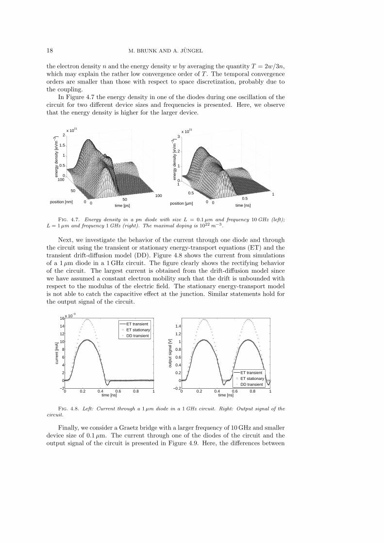
In Figure 4.7 the energy density in one of the diodes during one oscillation of thecircuit for two different device sizes and frequencies is presented. Here, we observethat the energy density is higher for the larger device.
050
100
0
50
1000
0.5
1
1.5
2x 10
21
time [ps]position [nm]
ener
gy d
ensi
ty [e
Vm
−3 ]
00.5
1
0
0.5
10
1
2
3x 10
21
time [ns]position [µm]
ener
gy d
ensi
ty [e
Vm
−3 ]
Fig. 4.7. Energy density in a pn diode with size L = 0.1 µm and frequency 10GHz (left);L = 1 µm and frequency 1GHz (right). The maximal doping is 1022 m−3.
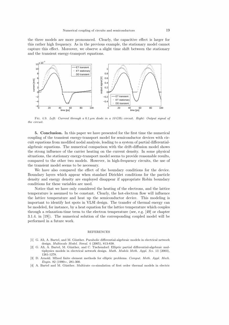
Next, we investigate the behavior of the current through one diode and throughthe circuit using the transient or stationary energy-transport equations (ET) and thetransient drift-diffusion model (DD). Figure 4.8 shows the current from simulationsof a 1µm diode in a 1 GHz circuit. The figure clearly shows the rectifying behaviorof the circuit. The largest current is obtained from the drift-diffusion model sincewe have assumed a constant electron mobility such that the drift is unbounded withrespect to the modulus of the electric field. The stationary energy-transport modelis not able to catch the capacitive effect at the junction. Similar statements hold forthe output signal of the circuit.
0 0.2 0.4 0.6 0.8 1−2
0
2
4
6
8
10
12
14
16x 10
−3
time [ns]
curr
ent [
mA
]
ET transient
ET stationary
DD transient
0 0.2 0.4 0.6 0.8 1−0.2
0
0.2
0.4
0.6
0.8
1
1.2
1.4
time [ns]
outp
ut s
igna
l [V
]
ET transient
ET stationary
DD transient
Fig. 4.8. Left: Current through a 1 µm diode in a 1GHz circuit. Right: Output signal of thecircuit.
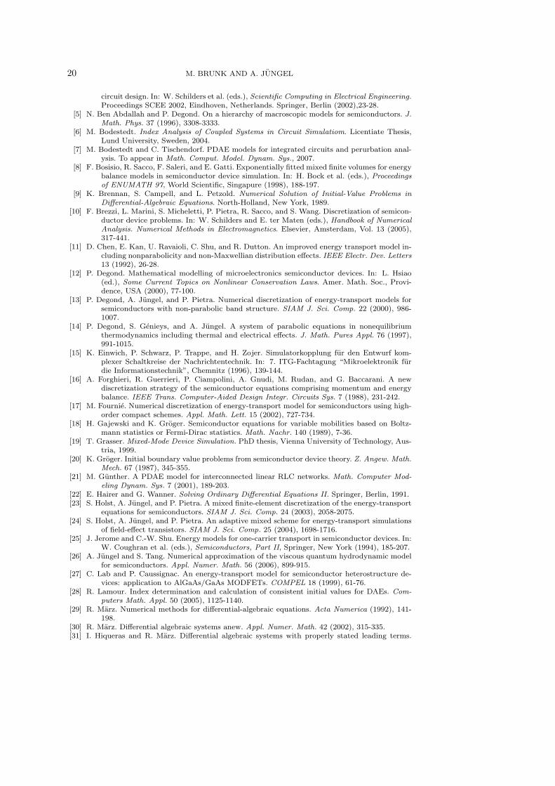
Finally, we consider a Graetz bridge with a larger frequency of 10 GHz and smallerdevice size of 0.1µm. The current through one of the diodes of the circuit and theoutput signal of the circuit is presented in Figure 4.9. Here, the differences between
Numerical coupling of circuits and semiconductors 19
the three models are more pronounced. Clearly, the capacitive effect is larger forthis rather high frequency. As in the previous example, the stationary model cannotcapture this effect. Moreover, we observe a slight time shift between the stationaryand the transient energy-transport equations.
0 20 40 60 80 100−6
−4
−2
0
2
4
6
8
10
12x 10
−3
time [ps]
curr
ent [
mA
]
ET transient
ET stationary
DD transient
0 20 40 60 80 100
−0.4
−0.2
0
0.2
0.4
0.6
0.8
1
time [ps]
outp
ut s
igna
l [V
]
ET transient
ET stationary
DD transient
Fig. 4.9. Left: Current through a 0.1 µm diode in a 10GHz circuit. Right: Output signal ofthe circuit.
5. Conclusion. In this paper we have presented for the first time the numericalcoupling of the transient energy-transport model for semiconductor devices with cir-cuit equations from modified nodal analysis, leading to a system of partial differential-algebraic equations. The numerical comparison with the drift-diffusion model showsthe strong influence of the carrier heating on the current density. In some physicalsituations, the stationary energy-transport model seems to provide reasonable results,compared to the other two models. However, in high-frequency circuits, the use ofthe transient model seems to be necessary.
We have also compared the effect of the boundary conditions for the device.Boundary layers which appear when standard Dirichlet conditions for the particledensity and energy density are employed disappear if appropriate Robin boundaryconditions for these variables are used.
Notice that we have only considered the heating of the electrons, and the latticetemperature is assumed to be constant. Clearly, the hot-electron flow will influencethe lattice temperature and heat up the semiconductor device. This modeling isimportant to identify hot spots in VLSI design. The transfer of thermal energy canbe modeled, for instance, by a heat equation for the lattice temperature which couplesthrough a relaxation-time term to the electron temperature (see, e.g. [49] or chapter3.1.4. in [19]). The numerical solution of the corresponding coupled model will beperformed in a future work.
REFERENCES
[1] G. Alı, A. Bartel, and M. Gunther. Parabolic differential-algebraic models in electrical networkdesign. Multiscale Model. Simul. 4 (2005), 813-838.
[2] G. Alı, A. Bartel, M. Gunther, and C. Tischendorf. Elliptic partial differential-algebraic mul-tiphysics models in electrical network design. Math. Models Meth. Appl. Sci. 13 (2003),1261-1278.
[3] D. Arnold. MIxed finite element methods for elliptic problems. Comput. Meth. Appl. Mech.Engin. 82 (1990=, 281-300.
[4] A. Bartel and M. Gunther. Multirate co-simulation of first order thermal models in electric
20 M. BRUNK AND A. JUNGEL
circuit design. In: W. Schilders et al. (eds.), Scientific Computing in Electrical Engineering.Proceedings SCEE 2002, Eindhoven, Netherlands. Springer, Berlin (2002),23-28.
[5] N. Ben Abdallah and P. Degond. On a hierarchy of macroscopic models for semiconductors. J.Math. Phys. 37 (1996), 3308-3333.
[6] M. Bodestedt. Index Analysis of Coupled Systems in Circuit Simulatiom. Licentiate Thesis,Lund University, Sweden, 2004.
[7] M. Bodestedt and C. Tischendorf. PDAE models for integrated circuits and perurbation anal-ysis. To appear in Math. Comput. Model. Dynam. Sys., 2007.
[8] F. Bosisio, R. Sacco, F. Saleri, and E. Gatti. Exponentially fitted mixed finite volumes for energybalance models in semiconductor device simulation. In: H. Bock et al. (eds.), Proceedingsof ENUMATH 97, World Scientific, Singapure (1998), 188-197.
[9] K. Brennan, S. Campell, and L. Petzold. Numerical Solution of Initial-Value Problems inDifferential-Algebraic Equations. North-Holland, New York, 1989.
[10] F. Brezzi, L. Marini, S. Micheletti, P. Pietra, R. Sacco, and S. Wang. Discretization of semicon-ductor device problems. In: W. Schilders and E. ter Maten (eds.), Handbook of NumericalAnalysis. Numerical Methods in Electromagnetics. Elsevier, Amsterdam, Vol. 13 (2005),317-441.
[11] D. Chen, E. Kan, U. Ravaioli, C. Shu, and R. Dutton. An improved energy transport model in-cluding nonparabolicity and non-Maxwellian distribution effects. IEEE Electr. Dev. Letters13 (1992), 26-28.
[12] P. Degond. Mathematical modelling of microelectronics semiconductor devices. In: L. Hsiao(ed.), Some Current Topics on Nonlinear Conservation Laws. Amer. Math. Soc., Provi-dence, USA (2000), 77-100.
[13] P. Degond, A. Jungel, and P. Pietra. Numerical discretization of energy-transport models forsemiconductors with non-parabolic band structure. SIAM J. Sci. Comp. 22 (2000), 986-1007.
[14] P. Degond, S. Genieys, and A. Jungel. A system of parabolic equations in nonequilibriumthermodynamics including thermal and electrical effects. J. Math. Pures Appl. 76 (1997),991-1015.
[15] K. Einwich, P. Schwarz, P. Trappe, and H. Zojer. Simulatorkopplung fur den Entwurf kom-plexer Schaltkreise der Nachrichtentechnik. In: 7. ITG-Fachtagung “Mikroelektronik furdie Informationstechnik”, Chemnitz (1996), 139-144.
[16] A. Forghieri, R. Guerrieri, P. Ciampolini, A. Gnudi, M. Rudan, and G. Baccarani. A newdiscretization strategy of the semiconductor equations comprising momentum and energybalance. IEEE Trans. Computer-Aided Design Integr. Circuits Sys. 7 (1988), 231-242.
[17] M. Fournie. Numerical discretization of energy-transport model for semiconductors using high-order compact schemes. Appl. Math. Lett. 15 (2002), 727-734.
[18] H. Gajewski and K. Groger. Semiconductor equations for variable mobilities based on Boltz-mann statistics or Fermi-Dirac statistics. Math. Nachr. 140 (1989), 7-36.
[19] T. Grasser. Mixed-Mode Device Simulation. PhD thesis, Vienna University of Technology, Aus-tria, 1999.
[20] K. Groger. Initial boundary value problems from semiconductor device theory. Z. Angew. Math.Mech. 67 (1987), 345-355.
[21] M. Gunther. A PDAE model for interconnected linear RLC networks. Math. Computer Mod-eling Dynam. Sys. 7 (2001), 189-203.
[22] E. Hairer and G. Wanner. Solving Ordinary Differential Equations II. Springer, Berlin, 1991.[23] S. Holst, A. Jungel, and P. Pietra. A mixed finite-element discretization of the energy-transport
equations for semiconductors. SIAM J. Sci. Comp. 24 (2003), 2058-2075.[24] S. Holst, A. Jungel, and P. Pietra. An adaptive mixed scheme for energy-transport simulations
of field-effect transistors. SIAM J. Sci. Comp. 25 (2004), 1698-1716.[25] J. Jerome and C.-W. Shu. Energy models for one-carrier transport in semiconductor devices. In:
W. Coughran et al. (eds.), Semiconductors, Part II, Springer, New York (1994), 185-207.[26] A. Jungel and S. Tang. Numerical approximation of the viscous quantum hydrodynamic model
for semiconductors. Appl. Numer. Math. 56 (2006), 899-915.[27] C. Lab and P. Caussignac. An energy-transport model for semiconductor heterostructure de-
vices: application to AlGaAs/GaAs MODFETs. COMPEL 18 (1999), 61-76.[28] R. Lamour. Index determination and calculation of consistent initial values for DAEs. Com-
puters Math. Appl. 50 (2005), 1125-1140.[29] R. Marz. Numerical methods for differential-algebraic equations. Acta Numerica (1992), 141-
198.[30] R. Marz. Differential algebraic systems anew. Appl. Numer. Math. 42 (2002), 315-335.[31] I. Hiqueras and R. Marz. Differential algebraic systems with properly stated leading terms.
Numerical coupling of circuits and semiconductors 21
Comput. Math. Appl. 48 (2004), 215-235.[32] L. D. Marini and P. Pietra. An abstract theory for mixed approximations of second order elliptic
equations. Mat. Aplic. Comp. 8 (1989), 219-239.[33] L. D. Marini and P. Pietra. New mixed finite element schemes for current continuity equations.
COMPEL 9 (1990), 257-268.[34] A. Marrocco and P. Montarnal. Simulation of energy-transport models via mixed finite elements.
C. R. Acad. Sci., Paris, Ser. I 323 (1996), 535-541.[35] J. Litsios, B. Schmithusen, U. Krumbein, A. Schenk, E. Lyumkis, B. Polsky, and W. Fichtner.
DESSIS 3.0 Manual. ISE Integrated Systems Engineering, Zurich, 1996.[36] K. Pipe, R. Ram, and A. Shakouri. Bias-dependent Peltier coefficient and internal heating in
bipolar devices. Phys. Rev. B 66 (2002), 125316.[37] P. Raviart and J. Thomas. A mixed finite element method for second order elliptic equations.
In: Mathematical Aspects of the Finite Element Method, Proc. Conf. Rome 1975. LectureNotes in Mathematics 606 (1977), 292-315.
[38] C. Ringhofer. An entropy-based finite difference method for the energy transport system. Math.Models Meth. Appl. Sci. 11 (2001), 769-796.
[39] F. Rotella. Mixed circuit and device simulation for analysis, design, and optimization of opto-electronic, radio frequency, and high speed semiconductor devices. PhD thesis, StanfordUniversity, 2000.
[40] M. Rudan, A. Gnudi, and W. Quade. A generalized approach to the hydrodynamic model ofsemiconductor equations. In: G. Baccarani (ed.), Process and Device Modeling for Micro-electronics, Elsevier, Amsterdam (1993), 109-154.
[41] D. Schroder. Carrier lifetimes in silicon. IEEE Trans. Electron Dev. 44 (1997), 160-170.[42] M. Selva Soto and C. Tischendorf. Numerical analysis of DAEs from coupled circuit and semi-
conductor simulation. Appl. Numer. Math. 53 (2005), 471-488.[43] K. Souissi, F. Odeh, H. Tang, and A. Gnudi. Comparative studies of hydrodynamic and energy
transport models. COMPEL 13 (1994), 439-453.[44] R. Stratton. Diffusion of hot and cold electrons in semiconductor barriers. Phys. Rev. 126
(1962), 2002-2014.[45] C. Tischendorf. Solution of Index-2 Differential-Algebraic Equations and Its Application to
Circuit Simulation. PhD thesis, Humboldt-Universitat zu Berlin, 1996.[46] C. Tischendorf. Topological index calculation of differential-algebraic equations in circuit sim-
ulation. Surveys Math. Industr. 8 (1999), 187-199.[47] C. Tischendorf. Modeling circuit systems coupled with distributed semiconductor equations.
In: K. Antreich, R. Bulirsch, A. Gilg, and P. Rentrop (eds.), Modeling, Simulation, andOptimization of Integrated Circuits, Internat. Series Numer. Math. 146 (2003), 229-247.
[48] C. Tischendorf. Coupled systems of differential algebraic and partial differential equations incircuit and device simulations. Habilitation thesis, Humboldt Universitat zu Berlin, 2003.
[49] G. Wachutka. Rigorous thermodynamic treatment of heat generation and conduction in semi-conductor device modeling. IEEE Trans. Computer-Aided Design 9 (1990), 1141-1149.
[50] A. Yamnahakki. Second-order boundary conditions for the drift-diffusion equations for semi-conductors. Math. Models Meth. Appl. Sci. 5 (1995), 429-455.